i.MX 8M Nano Hardware Developer’s Guide• Electromagnetic Compatibility Engineering - Henry Ott...
44
© 2019 NXP B.V. i.MX 8M Nano Hardware Developer’s Guide 1. Overview This document aims to help hardware engineers design and test the i.MX 8M Nano series processors. It provides examples on board layout and design checklists to ensure first-pass success, and solutions to avoid board bring-up problems. Engineers should understand board layouts and board hardware terminology. This guide is released with relevant device-specific hardware documentation, such as datasheets, reference manuals, and application notes. All these documents are available on www.nxp.com/imx8mnanoevk. 1.1. Device supported This document supports the i.MX 8M Nano (14 x 14 mm package). NXP Semiconductors Document Number: IMX8MNHDG User's Guide Rev. 0 , 12/2019 Contents 1. Overview ............................................................................ 1 1.1. Device supported..................................................... 1 1.2. Essential references ................................................. 2 1.3. Supplementary references ....................................... 2 1.4. Related documentation ............................................ 3 1.5. Conventions ............................................................ 3 1.6. Acronyms and abbreviations ................................... 4 2. i.MX 8M Nano design checklist ......................................... 5 2.1. Design checklist table.............................................. 5 2.2. JTAG signal termination ....................................... 13 2.3. Signal termination for Boundary-scan................... 13 3. i.MX 8M Nano layout/routing recommendations............. 13 3.1. Introduction ........................................................... 13 3.2. Basic design recommendations ............................. 13 3.3. Stack-up and manufacturing recommendations..... 14 3.4. DDR design recommendations.............................. 17 3.5. Trace impedance recommendations ...................... 27 3.6. Power connectivity/routing ................................... 28 3.7. USB connectivity .................................................. 30 3.8. Unused input/output terminations ......................... 31 4. Avoiding board bring-up problems .................................. 31 4.1. Introduction ........................................................... 31 4.2. Avoiding power pitfalls -Current .......................... 32 4.3. Avoiding power pitfalls -Voltage .......................... 32 4.4. Checking for clock pitfalls .................................... 33 4.5. Avoiding reset pitfalls ........................................... 33 4.6. Sample board bring-up checklist ........................... 33 5. Using BSDL for Board-level Testing ............................... 35 5.1. BSDL overview..................................................... 35 5.2. How BSDL functions ............................................ 35 5.3. Downloading the BSDL file .................................. 35 5.4. Pin coverage of BSDL........................................... 36 5.5. Boundary scan operation ....................................... 36 5.6. I/O pin power considerations ................................ 38 6. Thermal Considerations ................................................... 38 6.1. Introduction ........................................................... 38 6.2. PCB Dimensions ................................................... 39 6.3. Copper Volume ..................................................... 39 6.4. Thermal Resistance ............................................... 40 6.5. Power Net Design ................................................. 40 6.6. Component Placement........................................... 41 6.7. PCB Surroundings................................................. 41 6.8. Thermal Simulations ............................................. 42 6.9. Software optimization ........................................... 42 6.10. The Thermal Checklist .......................................... 42 7. Revision history ............................................................... 43
Transcript of i.MX 8M Nano Hardware Developer’s Guide• Electromagnetic Compatibility Engineering - Henry Ott...
© 2019 NXP B.V.
i.MX 8M Nano Hardware Developer’s Guide
1. Overview
This document aims to help hardware engineers design
and test the i.MX 8M Nano series processors. It provides
examples on board layout and design checklists to ensure
first-pass success, and solutions to avoid board bring-up
problems.
Engineers should understand board layouts and board
hardware terminology.
This guide is released with relevant device-specific
hardware documentation, such as datasheets, reference
manuals, and application notes. All these documents are
available on www.nxp.com/imx8mnanoevk.
1.1. Device supported
This document supports the i.MX 8M Nano (14 x 14 mm
package).
NXP Semiconductors Document Number: IMX8MNHDG
User's Guide Rev. 0 , 12/2019
Contents
1. Overview ............................................................................ 1 1.1. Device supported ..................................................... 1 1.2. Essential references ................................................. 2 1.3. Supplementary references ....................................... 2 1.4. Related documentation ............................................ 3 1.5. Conventions ............................................................ 3 1.6. Acronyms and abbreviations ................................... 4
2. i.MX 8M Nano design checklist ......................................... 5 2.1. Design checklist table.............................................. 5 2.2. JTAG signal termination ....................................... 13 2.3. Signal termination for Boundary-scan ................... 13
3. i.MX 8M Nano layout/routing recommendations ............. 13 3.1. Introduction ........................................................... 13 3.2. Basic design recommendations ............................. 13 3.3. Stack-up and manufacturing recommendations ..... 14 3.4. DDR design recommendations .............................. 17 3.5. Trace impedance recommendations ...................... 27 3.6. Power connectivity/routing ................................... 28 3.7. USB connectivity .................................................. 30 3.8. Unused input/output terminations ......................... 31
4. Avoiding board bring-up problems .................................. 31 4.1. Introduction ........................................................... 31 4.2. Avoiding power pitfalls -Current .......................... 32 4.3. Avoiding power pitfalls -Voltage .......................... 32 4.4. Checking for clock pitfalls .................................... 33 4.5. Avoiding reset pitfalls ........................................... 33 4.6. Sample board bring-up checklist ........................... 33
5. Using BSDL for Board-level Testing ............................... 35 5.1. BSDL overview ..................................................... 35 5.2. How BSDL functions ............................................ 35 5.3. Downloading the BSDL file .................................. 35 5.4. Pin coverage of BSDL........................................... 36 5.5. Boundary scan operation ....................................... 36 5.6. I/O pin power considerations ................................ 38
6. Thermal Considerations ................................................... 38 6.1. Introduction ........................................................... 38 6.2. PCB Dimensions ................................................... 39 6.3. Copper Volume ..................................................... 39 6.4. Thermal Resistance ............................................... 40 6.5. Power Net Design ................................................. 40 6.6. Component Placement........................................... 41 6.7. PCB Surroundings ................................................. 41 6.8. Thermal Simulations ............................................. 42 6.9. Software optimization ........................................... 42 6.10. The Thermal Checklist .......................................... 42
7. Revision history ............................................................... 43

Overview
i.MX 8M Nano Hardware Developer’s Guide, User's Guide, Rev. 0, 12/2019
2 NXP Semiconductors
1.2. Essential references
This guide is supplementary to the i.MX 8M Nano series chip reference manuals and data sheets. For
reflow profile and thermal limits during soldering, see General Soldering Temperature Process
Guidelines (document AN3300). These documents are available on www.nxp.com/i.MX8MNANO.
1.3. Supplementary references
1.3.1. General information
The following documents introduces the Arm® processor architecture and computer architecture.
• For information about the Arm Cortex-A53 processor, see:
https://www.arm.com/products/processors/cortex-a/cortex-a53-processor.php
• For information about the Arm Cortex-M7 processor, see:
https://www.arm.com/products/processors/cortex-m/cortex-m7-processor.php
• Computer Architecture: A Quantitative Approach (Fourth Edition) - by John L. Hennessy and
David A. Patterson
• Computer Organization and Design: The Hardware/Software Interface (Second Edition), by David
A. Patterson and John L. Hennessy
The following documentation introduces the high-speed board design:
• Right the First Time- A Practical Handbook on High Speed PCB and System Design - Volumes I
& II - Lee W. Ritchey (Speeding Edge) - ISBN 0-9741936- 0-72
• Signal and Power Integrity Simplified (2nd Edition) - Eric Bogatin (Prentice Hall)- ISBN 0-13-
703502-0
• High Speed Digital Design- A Handbook of Black Magic - Howard W. Johnson & Martin Graham
(Prentice Hall) - ISBN 0-13-395724-1
• High Speed Signal Propagation- Advanced Black Magic - Howard W. Johnson & Martin Graham -
(Prentice Hall) - ISBN 0-13-084408-X
• High Speed Digital System Design- A handbook of Interconnect Theory and Practice - Hall, Hall
and McCall (Wiley Interscience 2000) - ISBN 0-36090-2
• Signal Integrity Issues and Printed Circuit Design - Doug Brooks (Prentice Hall) ISBN 0-13-
141884-X
• PCB Design for Real-World EMI Control - Bruce R. Archambeault (Kluwer Academic Publishers
Group) - ISBN 1-4020-7130-2
• Digital Design for Interference Specifications - A Practical Handbook for EMI Suppression -David
L. Terrell & R. Kenneth Keenan (Newnes Publishing) - ISBN 0-7506-7282-X
• Electromagnetic Compatibility Engineering - Henry Ott (1st Edition - John Wiley and Sons) -
ISBN 0-471-85068-3
• Introduction to Electromagnetic Compatibility - Clayton R. Paul (John Wiley and Sons) - ISBN
978-0-470-18930-6

Overview
i.MX 8M Nano Hardware Developer’s Guide, User's Guide, Rev. 0, 12/2019
NXP Semiconductors 3
• Grounding & Shielding Techniques - Ralph Morrison (5th Edition - John Wiley & Sons) - ISBN 0-
471-24518-6
• EMC for Product Engineers - Tim Williams (Newnes Publishing) - ISBN 0-7506- 2466-3
1.4. Related documentation
Additional literature will be published when new NXP products become available.
For the list of current documents, see www.nxp.com/i.MX8MNANO.
1.5. Conventions
Table 1 lists the notational conventions used in this document.
Table 1. Conventions used in the document
Conventions Description
Courier Used to indicate commands, command parameters, code examples, and file and directory names.
Italics Used to indicates command or function parameters.
Bold Function names are written in bold.
cleared/set When a bit takes the value zero, it means to be cleared; when it takes a value of one, it means to be set.
mnemonics Instruction mnemonics are shown in lowercase bold. Book titles in text are set in italics.
sig_name Internal signals are written in all lowercase.
nnnn nnnnh Denotes hexadecimal number
0b Denotes binary number
rA, rB Instruction syntax used to identify a source GPR
rD Instruction syntax used to identify a destination GPR
REG[FIELD] Abbreviations for registers are shown in uppercase. Specific bits, fields, or ranges appear in brackets.
For example, MSR[LE] refers to the little-endian mode enable bit in the machine state register.
x An italicized x indicates an alphanumeric variable.
n, m An italicized n indicates a numeric variable.
In this guide, notation for all logical, bit-wise, arithmetic, comparison, and assignment operations follow
C Language conventions.
Overview
i.MX 8M Nano Hardware Developer’s Guide, User's Guide, Rev. 0, 12/2019
4 NXP Semiconductors
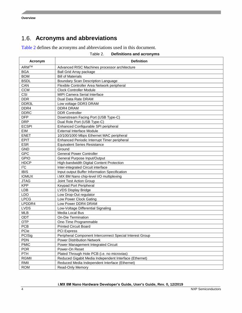
1.6. Acronyms and abbreviations
Table 2 defines the acronyms and abbreviations used in this document.
Table 2. Definitions and acronyms
Acronym Definition
ARMTM Advanced RISC Machines processor architecture
BGA Ball Grid Array package
BOM Bill of Materials
BSDL Boundary Scan Description Language
CAN Flexible Controller Area Network peripheral
CCM Clock Controller Module
CSI MIPI Camera Serial Interface
DDR Dual Data Rate DRAM
DDR3L Low voltage DDR3 DRAM
DDR4 DDR4 DRAM
DDRC DDR Controller
DFP Downstream Facing Port (USB Type-C)
DRP Dual Role Port (USB Type-C)
ECSPI Enhanced Configurable SPI peripheral
EIM External Interface Module
ENET 10/100/1000 Mbps Ethernet MAC peripheral
EPIT Enhanced Periodic Interrupt Timer peripheral
ESR Equivalent Series Resistance
GND Ground
GPC General Power Controller
GPIO General Purpose Input/Output
HDCP High-bandwidth Digital Content Protection
I2C Inter-integrated Circuit interface
IBIS Input output Buffer Information Specification
IOMUX i.MX 8M Nano chip-level I/O multiplexing
JTAG Joint Test Action Group
KPP Keypad Port Peripheral
LDB LVDS Display Bridge
LDO Low Drop-Out regulator
LPCG Low Power Clock Gating
LPDDR4 Low Power DDR4 DRAM
LVDS Low-Voltage Differential Signaling
MLB Media Local Bus
ODT On-Die Termination
OTP One-Time Programmable
PCB Printed Circuit Board
PCIe PCI Express
PCISig Peripheral Component Interconnect Special Interest Group
PDN Power Distribution Network
PMIC Power Management Integrated Circuit
POR Power-On Reset
PTH Plated Through Hole PCB (i.e. no microvias)
RGMII Reduced Gigabit Media Independent Interface (Ethernet)
RMII Reduced Media Independent Interface (Ethernet)
ROM Read-Only Memory

i.MX 8M Nano design checklist
i.MX 8M Nano Hardware Developer’s Guide, User's Guide, Rev. 0, 12/2019
NXP Semiconductors 5
2. i.MX 8M Nano design checklist
This document provides a design checklist for the i.MX 8M Nano (14 x 14 mm package) processor. The
design checklist tables recommend optimal design and provide explanations to help users understand
better. All supplemental tables referenced by the checklist appear in sections following the design
checklist tables.
2.1. Design checklist table
Table 3. LPDDR4 recommandations (i.MX 8M Nano)
Check box Recommendations Explanation/Supplemental recommendations
1. Connect the DRAM_ZN ball on the processor (ball P2) to a 240 Ω, 1% resistor to GND.
This is a reference used during DRAM output
buffer driver calibration.
2. The ZQ0 and ZQ1 balls on the LPDDR4 device should be connected through 240Ω, 1% resistors to the LPDDR4 VDD2 rail.
-
3. Place a 10 kΩ, 5% resistor to ground on the DRAM
reset signal.
This will ensure adherence to the JEDEC
specification until the control is configured and
starts driving the DDR.
4. The ODT_CA balls on the LPDDR4 device should
be connected directly to the LPDDR4 VDD2 rail.
LPDDR4 ODT on the i.MX 8M Nano is
command-based, making processor ODT_CA
output balls unnecessary.
5. The architecture for each chip inside the DRAM package must be x 16.
The processor does not support byte mode
specified in JESD209-4B.
6. The processor ball MTEST (ball N2), should be left unconnected.
These are observability ports for manufacturing
and are not used otherwise.
7. The VREF pin on the processor (ball P1) can be left unconnected.
The VREF signal for LPDDR4 is generated
internally by the processor.
8. It is strongly suggested to use LPDDR4 if lower power consumption is required since DLL-off mode is not supported.
The LPDDR4 can operate at low frequency
without DLL-off mode.
9. VDD_DRAM should be always on during DDR retention mode. Otherwise the data in DRAM might be lost when exiting this mode.
See Errata e50381 for detailed information.
Table 4. DDR4/DDR3L recommendations (i.MX 8M Nano)
Check box Recommendations Explanation/Supplemental recommendations
1. Connect the ZQ(DRAM_ZN) ball on the processor (ball P2) to individual 240 Ω, 1% resistors to GND.
This is a reference used during DRAM output
buffer driver calibration.
2. The ZQ ball on each DDR4/DDR3L device should be connected through individual 240 Ω, 1% resistors to GND.
-
3. Place a 10 kΩ, 5% resistor to ground on the DRAM reset signal.
This will ensure adherence to the JEDEC
specification until the control is configured and
starts driving the DDR.
4. The processor ball MTEST (ball N2), should be left unconnected.
These are observability ports for manufacturing
and are not used otherwise.
5. Using x16 bit board to test the x8 bit DDR feature, only the controller setting is different, the PHY should train as x16 bit device.
Using x8 bit setting for initial and train on a x16 bit board, it may cause some issues, such as:
• BG issue
• PDA(Per DRAM Accessibility) based train issue.

i.MX 8M Nano design checklist
i.MX 8M Nano Hardware Developer’s Guide, User's Guide, Rev. 0, 12/2019
6 NXP Semiconductors
Table 4. DDR4/DDR3L recommendations (i.MX 8M Nano)
Check box Recommendations Explanation/Supplemental recommendations
6. DLL-off mode isn’t supported, which means DDR4/DDR3L can’t run in low frequency such as 100MTS.
The power consumption for low power mode in DDR4/DDR3L system will be higher compared with LPDDR4 system.
7. VDD_DRAM should be always on during DDR retention mode. Otherwise the data in DRAM might be lost when exiting this mode.
See Errata e50381 for detailed information.
Table 5. I2C recommendations
Check box Recommendations Explanation/Supplemental recommendations
1. Verify the target I2C interface clock rates
The I2C bus can only be operated as fast as the
slowest peripheral on the bus. If faster operation
is required, move the slow devices to another
I2C port.
2. Verify that there are no I2C address conflicts on any of the I2C buses utilized
There are multiple I2C ports available on chip,
so if a conflict exists, move one of the conflicting
devices to a different I2C bus. If it is impossible,
use a I2C bus switch (NXP part number
PCA9646).
3. Do not place more than one set of pull-up resistors on the I2C lines.
This could result in excessive loading and
potential incorrect operation. Choose the pull-up
value commensurate with the bus speed being
used.
4. Ensure that the VCC rail powering the i.MX 8M Nano I2C interface balls matches the supply voltage used for the pull-up resistors and the slave I2C devices.
Prevent device damage or incorrect operation
due to voltage mismatch.
Table 6. JTAG recommendations
Check box Recommendations Explanation/Supplemental recommendations
1. Do not use external pullup or pulldown resistors on
JTAG_TDO.
JTAG_TDO is configured with an on-chip
keeper circuit and the floating condition is
actively eliminated.
2. Follow the recommendations for external pull-up and pull-down resistors given in Table 18.
-
3. JTAG_MOD should be connected to ground through a resistor.
-
4. JTAG_TMS pin must be connected with a 50ohm series resistor near the component if used or fanout. Otherwise, floating if not fanout.
-
Table 7. Reset and ON/OFF recommendations
Check box Recommendations Explanation/Supplemental recommendations
1. The POR_B input must be asserted at powered up and remain asserted until the last power rail for devices required for system boot are at their working voltage. This functionality is controlled by the PMIC on EVK.
POR_B is driven by the PMIC. If a reset button
is used, it should be connected to the
PWRON_B pin of the PMIC instead of directly
connected to POR_B pin of the CPU. When
POR_B is asserted (low) on the i.MX 8M Nano,
the output PMIC_ON_REQ remains asserted
(high).

i.MX 8M Nano design checklist
i.MX 8M Nano Hardware Developer’s Guide, User's Guide, Rev. 0, 12/2019
NXP Semiconductors 7
Table 7. Reset and ON/OFF recommendations
Check box Recommendations Explanation/Supplemental recommendations
2. For portable applications, the ONOFF pin may be connected to an ON/OFF SPST push-button switch to ground. An external pull-up resistor is required on this pin.
A brief connection to GND in OFF mode causes
the internal power management state machine
to change state to ON. In ON mode, a brief
connection to GND generates an interrupt
(intended to initiate a software-controllable
power-down). The connection to GND for
approximate 5 seconds or more causes a forced
OFF.
3. Connect GPIO1_IO02( WDOG_B, ball AG13) to
external PMIC or reset IC to repower the system except SNVS is strongly recommended.
i.MX8M Nano can't be reset by internal reset
source in idle mode, repower is preferred. Some
peripherals like SD3.0, QSPI also need repower
during system reset.
4. GPIO1_IO02( WDOG_B, ball AG13) is used as Cold Reset. If the PMIC enable the WDOG_B reset by default, external pull up resistor (100Kohm) and WDOG timer buffer are needed to support boundary-scan mode.
During entering boundary scan mode,
WDOG_B is always low. Without the WDOG
timer buffer and external 100Kohm pull up,
WDOG_B will repeatedly reset 8MNANOD4-
EVK when entering boundary-scan mode. See
section 5.5. Boundary scan operation for more
details.
Table 8. USB recommendations
Check box Recommendations Explanation/Supplemental recommendations
1. The USB1_TXRTUNE (ball E19) must be connected with a 200 Ω, 1% resistor to the ground.
-
2. The USB1_VBUS (ball F22) must be connected
with a 30K Ω, 1% series resistor to 5V VBUS power.
The USB1_VBUS pin must not connect directly to the 5V VBUS voltage. This pin must be isolated by an external resistor (30K Ω, 1%) so that the USB1_VBUS pin sees a lower voltage.
3. Route all USB differential signals with 90 Ω differential impedance.
-
4. ESD protection should be implemented at the connector pins. Choose a low capacitance device recommended for high-speed interfaces.
This will prevent potential damages to board components from ESD.
i.MX 8M Nano design checklist
i.MX 8M Nano Hardware Developer’s Guide, User's Guide, Rev. 0, 12/2019
8 NXP Semiconductors
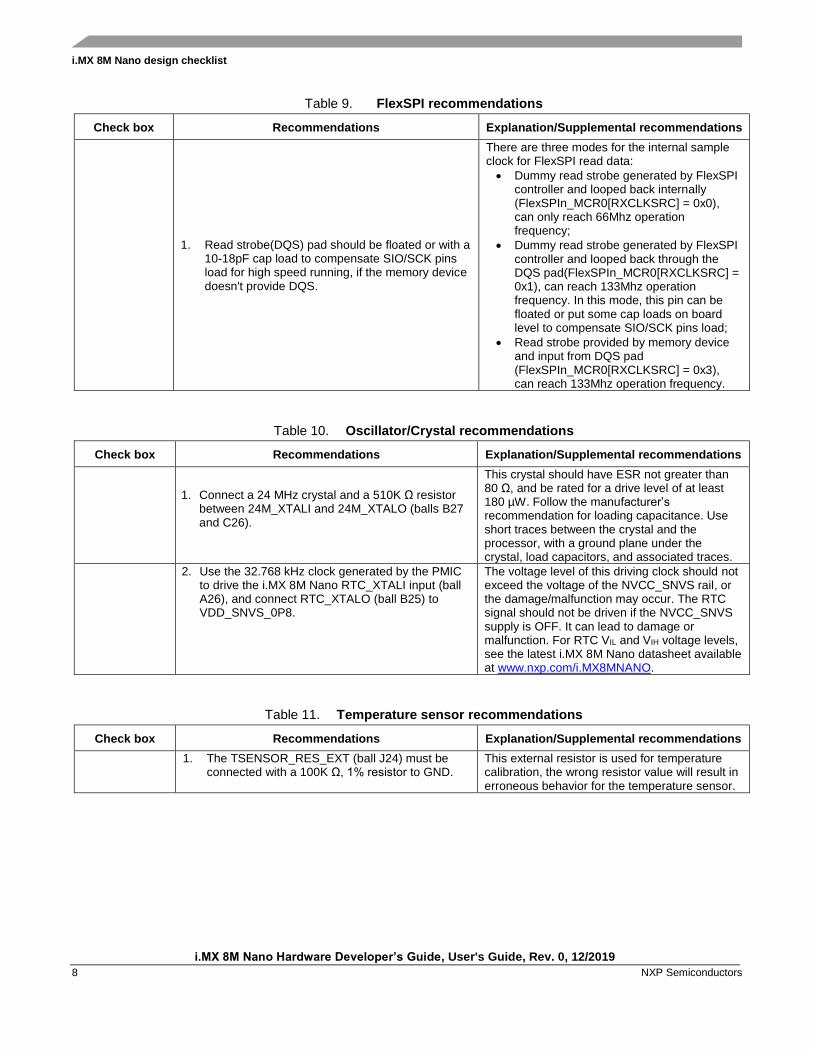
Table 9. FlexSPI recommendations
Check box Recommendations Explanation/Supplemental recommendations
1. Read strobe(DQS) pad should be floated or with a 10-18pF cap load to compensate SIO/SCK pins load for high speed running, if the memory device doesn't provide DQS.
There are three modes for the internal sample clock for FlexSPI read data:
• Dummy read strobe generated by FlexSPI controller and looped back internally (FlexSPIn_MCR0[RXCLKSRC] = 0x0), can only reach 66Mhz operation frequency;
• Dummy read strobe generated by FlexSPI controller and looped back through the DQS pad(FlexSPIn_MCR0[RXCLKSRC] = 0x1), can reach 133Mhz operation frequency. In this mode, this pin can be floated or put some cap loads on board level to compensate SIO/SCK pins load;
• Read strobe provided by memory device and input from DQS pad (FlexSPIn_MCR0[RXCLKSRC] = 0x3), can reach 133Mhz operation frequency.
Table 10. Oscillator/Crystal recommendations
Check box Recommendations Explanation/Supplemental recommendations
1. Connect a 24 MHz crystal and a 510K Ω resistor between 24M_XTALI and 24M_XTALO (balls B27 and C26).
This crystal should have ESR not greater than 80 Ω, and be rated for a drive level of at least 180 µW. Follow the manufacturer’s recommendation for loading capacitance. Use short traces between the crystal and the processor, with a ground plane under the crystal, load capacitors, and associated traces.
2. Use the 32.768 kHz clock generated by the PMIC to drive the i.MX 8M Nano RTC_XTALI input (ball A26), and connect RTC_XTALO (ball B25) to VDD_SNVS_0P8.
The voltage level of this driving clock should not exceed the voltage of the NVCC_SNVS rail, or the damage/malfunction may occur. The RTC signal should not be driven if the NVCC_SNVS supply is OFF. It can lead to damage or malfunction. For RTC VIL and VIH voltage levels, see the latest i.MX 8M Nano datasheet available at www.nxp.com/i.MX8MNANO.
Table 11. Temperature sensor recommendations
Check box Recommendations Explanation/Supplemental recommendations
1. The TSENSOR_RES_EXT (ball J24) must be connected with a 100K Ω, 1% resistor to GND.
This external resistor is used for temperature calibration, the wrong resistor value will result in erroneous behavior for the temperature sensor.

i.MX 8M Nano design checklist
i.MX 8M Nano Hardware Developer’s Guide, User's Guide, Rev. 0, 12/2019
NXP Semiconductors 9
Table 12. i.MX 8M Nano power/decoupling recommendations
Check box Recommendations Explanation/Supplemental recommendations
1. Comply with the power-up sequence guidelines as described in the datasheet to guarantee reliable operations of the device.
Any deviation from these sequences may result in the following situations:
• Excessive current during power-up phase
• Prevention of the device from booting
• Irreversible damage to the processor (worst case)
2. Maximum ripple voltage requirements
Common requirement for ripple noise peak-to-peak value should be less than 5% of the supply voltage nominal value.
3. If using BD71850MWV PMIC to provide power, make sure all the regulators except BUCK5/LDO4/LDO5 have output L/C components properly connected, even if unused.
Leaving any regulator except BUCK5/LDO4/LDO5 output open will lead to malfunction of the PMIC.
4. If using PCA9450B PMIC to provide power, make
sure the voltage sensing pin of each BUCK is tied to VSYS if unused.
The voltage sensing pins are R_SNSP3_CFG, R_SNSPx and BUCKxFB in PCA9450B. Leaving any BUCK output open, the PMIC will enter fault shutdown.
Table 13. Decoupling capacitors recommendations (i.MX 8M Nano)
Checkbox Supply 2.2 nF 0.22 µF 1 µF 4.7 µF 10 µF Notes
VDD_SOC,
VDD_DRAM,
VDD_GPU,
VDD_DRAM_PLL_0P8
- - 11 - 3
These 4 power rails are combined
together on EVK
NVCC_DRAM - - 6 - 2 -
VDD_ARM - - 5 - 1 -
VDD_SNVS_0P8 - 1 - - - -
NVCC_SNVS_1P8 - - 1 - - -
VDD_24M_XTAL_1P8 - 1 - - - -
VDD_DRAM_PLL_1P8 - - 1 - - -
PVCC_1P8 - 2 - - - -
VDD_ARM_PLL_1P8,
VDD_ANA0_1P8,
VDD_ANA1_1P8,
VDD_USB_1P8,
VDD_MIPI_1P8
- 4 - - 1 -
NVCC_SAI3,
NVCC_SAI5,
NVCC_ECSPI,
VDD_USB_3P3
- 4 - 1 - -
NVCC_JTAG,
NVCC_NAND,
NVCC_SAI2,
NVCC_GPIO1,
NVCC_I2C,
NVCC_UART,
NVCC_SD1,
NVCC_CLK
- 3 - - 1 -
NVCC_SD2 - 1 - - - -
NVCC_ENET - 1 - - - -

i.MX 8M Nano design checklist
i.MX 8M Nano Hardware Developer’s Guide, User's Guide, Rev. 0, 12/2019
10 NXP Semiconductors
Table 13. Decoupling capacitors recommendations (i.MX 8M Nano)
Checkbox Supply 2.2 nF 0.22 µF 1 µF 4.7 µF 10 µF Notes
VDD_ARM_PLL_0P8,
VDD_ANA_0P8,
VDD_USB_0P8,
- 1 - 1 - -
VDD_MIPI_1P2 - 1 - - - -
VDD_MIPI_0P8 - 1 - - - -
MIPI_VREG_CAP 1 - - - -
Must connect a 2.2nF capacitor
between MIPI_VREG_CAP (ball
D15) and GND.
Capacitor part number used on EVK:
• 2.2 nF --- GRM033R71C222KA88D
• 0.22 uF --- LMK063BJ224MP-F
• 1 uF --- 02016D105MAT2A
• 4.7 uF --- CL05A475KP5NRNC
• 10 uF --- ZRB15XR60J106ME12D
Table 14. Bulk/Bypass capacitors recommendations (BD71850MWV PMIC)
Checkbox Supply 1 µF 4.7 µF 10 µF 22 µF Notes
BUCK1
(VDD_SOC&DRAM&GPU) - - - 2
-
BUCK2
(VDD_ARM) - - - 2
-
BUCK6
(VDD_3V3) - - - 2
-
BUCK7
(VDD_1V8) - - - 2
-
BUCK8
(NVCC_DRAM) - - - 2
-
LDO1
(NVCC_SNVS_1V8) 1 - - -
-
LDO2
(VDD_SNVS_0V8) 1 - - -
-
LDO3
(VDDA_1V8) - 1 - - -
LDO6
(VDD_PHY_1V2) - 1 - - -
MUXSW_VOUT
(NVCC_SD2) - - 1 - -
Capacitor part number used on EVK:
• 1 uF --- 02016D105MAT2A
• 4.7 uF --- CL05A475KP5NRNC
• 10 uF --- GRM188R61A106KE69D
• 22 uF --- C1608X5R1A226M080AC
Table 15. Bulk/Bypass capacitors recommendations (PCA9450B PMIC)
Checkbox Supply 1 µF 2.2 µF 22 µF Notes

i.MX 8M Nano design checklist
i.MX 8M Nano Hardware Developer’s Guide, User's Guide, Rev. 0, 12/2019
NXP Semiconductors 11
Checkbox Supply 1 µF 2.2 µF 22 µF Notes
BUCK1
(VDD_SOC&DRAM&GPU) - - 2
BUCK2
(VDD_ARM) - - 2
-
BUCK4
(VDD_3V3) - - 1
-
BUCK5
(VDD_1V8) - - 1
-
BUCK6
(NVCC_DRAM) - - 1
-
LDO1
(NVCC_SNVS_1V8) 1 - -
-
LDO2
(VDD_SNVS_0V8) 1 - -
-
LDO3
(VDDA_1V8) - 1 - -
LDO4
(VDD_PHY_1V2) 1 - - -
LDO5
(NVCC_SD2) 1 - - -
Capacitor part number used on EVK:
• 1 uF --- 02016D105MAT2A
• 2.2 uF --- C1005X5R1A225K
• 22 uF --- C1608X5R1A226M080AC
Table 16. PCB design recommendations
Check box Recommendations Explanation/Supplemental recommendations
1. High-speed signal traces have reference plane in adjacent layer and are impedance controlled.
Controlled impedance is the key factor to have good signal integrity. Note that the reference plane can only be GND or the signal’s own I/O power. Do not use other nets as reference. For DRAM, only GND reference is accepted for maintaining impedance. The power plane reference can’t be as the sole impedance return.
2. High-speed signal traces never cross gap or slot in reference plane.
Crossing gap in reference plane will cause reflection and increase crosstalk.
3. Place at least one GND stitching via within 50 mils of signal via when switching reference planes.
GND stitching via can help keep impedance continuous and reduce via crosstalk.
4. Appropriate delay matching is done for parallel bus.
Signals within a bus should have delay time matched to maintain timing margin.
5. The true and complementary signal of a differential pair must have delay matched to within 1ps.
The true and complementary signal within a differential pair should have delay time tightly matched.
6. DDR interface passed SI simulation. Alternatively, directly copy the EVK DDR layout design.
Generally, SI simulation should be performed for DDR interface that runs at 3200 MT/s to ensure stable working. If this is not feasible, just copy the EVK DDR layout design as well as the board stack-up.

i.MX 8M Nano design checklist
i.MX 8M Nano Hardware Developer’s Guide, User's Guide, Rev. 0, 12/2019
12 NXP Semiconductors
Table 16. PCB design recommendations
Check box Recommendations Explanation/Supplemental recommendations
7. Place test point on key signals to ease debugging. When placing test point on high-speed signal traces, make sure its diameter is no more than 20mil and the test point be directly placed on the trace with no stub.
Test points can bring excessive capacitance and should be carefully handled on high-speed signal traces.
8. Decoupling capacitors are placed as close to IC power pins and GND pins as possible.
Tight routing to both power and ground is needed to provide optimum decoupling effectiveness.
i.MX 8M Nano layout/routing recommendations
i.MX 8M Nano Hardware Developer’s Guide, User's Guide, Rev. 0, 12/2019
NXP Semiconductors 13
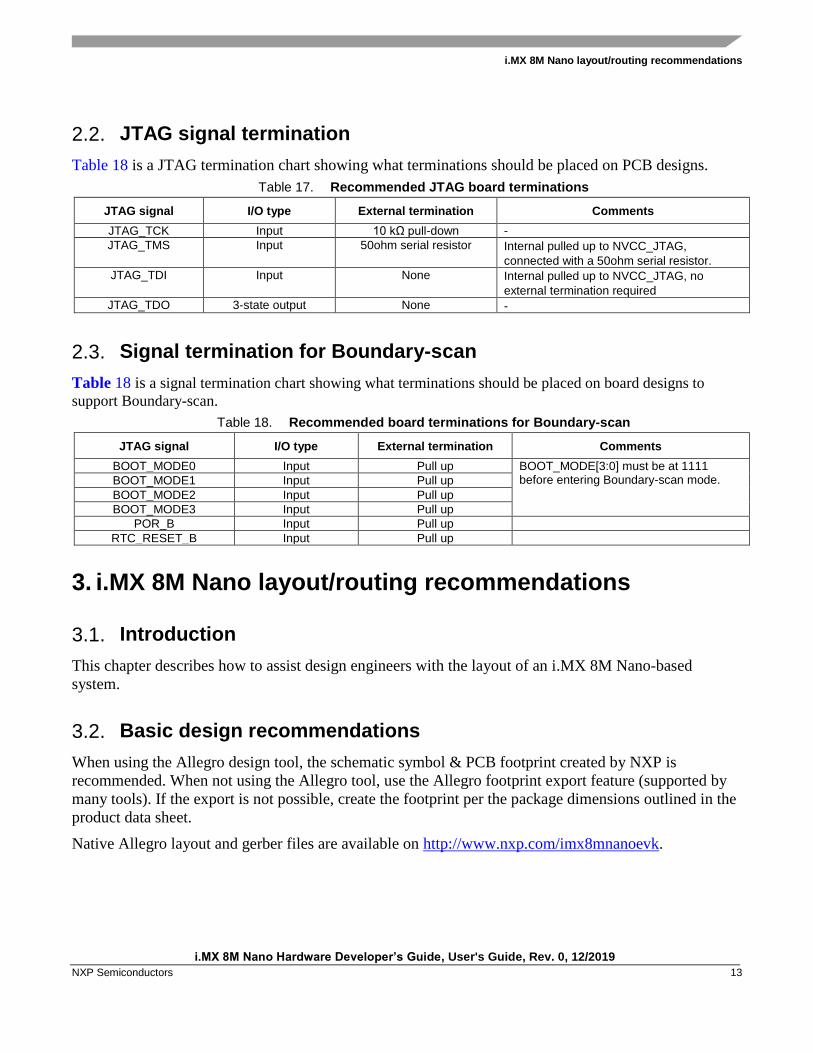
2.2. JTAG signal termination
Table 18 is a JTAG termination chart showing what terminations should be placed on PCB designs.
Table 17. Recommended JTAG board terminations
JTAG signal I/O type External termination Comments
JTAG_TCK Input 10 kΩ pull-down -
JTAG_TMS Input 50ohm serial resistor Internal pulled up to NVCC_JTAG,
connected with a 50ohm serial resistor.
JTAG_TDI Input None Internal pulled up to NVCC_JTAG, no
external termination required
JTAG_TDO 3-state output None -
2.3. Signal termination for Boundary-scan
Table 18 is a signal termination chart showing what terminations should be placed on board designs to
support Boundary-scan.
Table 18. Recommended board terminations for Boundary-scan
JTAG signal I/O type External termination Comments
BOOT_MODE0 Input Pull up BOOT_MODE[3:0] must be at 1111 before entering Boundary-scan mode. BOOT_MODE1 Input Pull up
BOOT_MODE2 Input Pull up
BOOT_MODE3 Input Pull up
POR_B Input Pull up
RTC_RESET_B Input Pull up
3. i.MX 8M Nano layout/routing recommendations
3.1. Introduction
This chapter describes how to assist design engineers with the layout of an i.MX 8M Nano-based
system.
3.2. Basic design recommendations
When using the Allegro design tool, the schematic symbol & PCB footprint created by NXP is
recommended. When not using the Allegro tool, use the Allegro footprint export feature (supported by
many tools). If the export is not possible, create the footprint per the package dimensions outlined in the
product data sheet.
Native Allegro layout and gerber files are available on http://www.nxp.com/imx8mnanoevk.
i.MX 8M Nano layout/routing recommendations
i.MX 8M Nano Hardware Developer’s Guide, User's Guide, Rev. 0, 12/2019
14 NXP Semiconductors
3.2.1. Placing decoupling capacitors
Place small decoupling and larger bulk capacitors on the bottom side of the PCB.
The 0201 or 0402 decoupling and 0603 or larger bulk capacitors should be mounted as close as possible
to the power vias. The distance should be less than 50 mils. Additional bulk capacitors can be placed
near the edge of the BGA via array. Placing the decoupling capacitors close to the power balls is critical
to minimize inductance and ensure high-speed transient current required by the processor. See the i.MX
8M Nano EVK layouts for examples of the desired decoupling capacitor placement.
The following list describes how to choose correct decoupling scheme:
• Place the largest capacitance in the smallest package that budget and manufacturing can support.
• For high-speed bypassing, select the required capacitance with the smallest package (for
example, 0.1 μF, 0.22 μF, 1.0 μF, or even 2.2 μF in a 0201 package size).
• Minimize trace length (inductance) to small caps.
• Series inductance cancels out capacitance.
• Tie caps to GND plane directly with a via.
• Place capacitors close to the power ball of the associated package from the schematic.
• A preferred BGA power decoupling design is available on the EVK board design available on
http://www.nxp.com/imx8mnanoevk. Customers should use the NXP design strategy for power
and decoupling.
3.3. Stack-up and manufacturing recommendations
3.3.1. Stack-up recommendation (i.MX 8M Nano)
Due to the number of balls on the i.MX 8M Nano processor in the 14 mm x 14 mm package, a minimum
6-layer PCB stack-up is recommended. For the 6-layers on the PCB, a sufficient number of layers need
to be dedicated to power on routing to meet the IR drop target of 2% for the i.MX 8M Nano CPU power
rails.
The constraints for the trace width will depend on such factors as the board stack-up and associated
dielectric and copper thickness, required impedance, and required current (for power traces). The stack-
up also determines the constraints for routing and spacing. Consider the following requirements when
designing the stack-up and selecting board material:
• Board stack-up is critical for high-speed signal quality.
• Preplanning impedance of critical traces is required.
• High-speed signals must have reference planes on adjacent layers to minimize cross-talk.
• PCB material: the material used on EVK is TU768.

i.MX 8M Nano layout/routing recommendations
i.MX 8M Nano Hardware Developer’s Guide, User's Guide, Rev. 0, 12/2019
NXP Semiconductors 15
3.3.2. Manufacturing recommendation (i.MX 8M Nano)
Since the i.MX 8M Nano processor uses 0.5mm-pitch BGA package, the PCB technology must meet
below requirement to fully fanout all the signals of the processor using PTH(plated through holes).
• Minimum trace width: 3.2mil
• Minimum trace to trace/pad spacing: 3.2mil
• Minimum via size: 8mil-diameter hole, 16mil-diameter pad
• Minimum via pad to pad spacing: 4mil
Figure 1 shows the reference routing of the i.MX 8M Nano, PTH is ok for the fanout, HDI is not
needed..
Figure 1. i.MX 8M Nano fanout routing on EVK
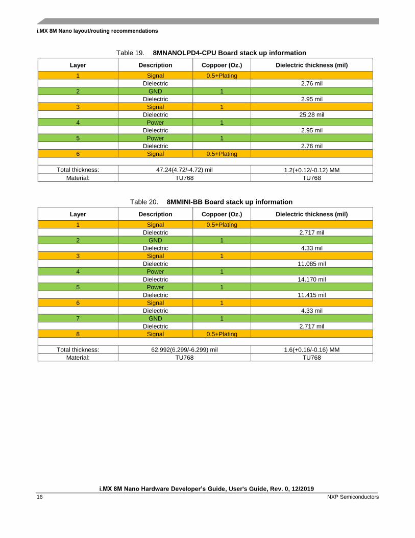
3.3.3. EVK PCB stack-up (i.MX 8M Nano)
Table 19 and Table 20 show stack-up of the EVK. The CPU board use 6-layer stack-up and the BB
board use 8-layer stack-up.
i.MX 8M Nano layout/routing recommendations
i.MX 8M Nano Hardware Developer’s Guide, User's Guide, Rev. 0, 12/2019
16 NXP Semiconductors
Table 19. 8MNANOLPD4-CPU Board stack up information
Layer Description Coppoer (Oz.) Dielectric thickness (mil)
1 Signal 0.5+Plating
Dielectric 2.76 mil
2 GND 1
Dielectric 2.95 mil
3 Signal 1
Dielectric 25.28 mil
4 Power 1
Dielectric 2.95 mil
5 Power 1
Dielectric 2.76 mil
6 Signal 0.5+Plating
Total thickness: 47.24(4.72/-4.72) mil 1.2(+0.12/-0.12) MM
Material: TU768 TU768
Table 20. 8MMINI-BB Board stack up information
Layer Description Coppoer (Oz.) Dielectric thickness (mil)
1 Signal 0.5+Plating
Dielectric 2.717 mil
2 GND 1
Dielectric 4.33 mil
3 Signal 1
Dielectric 11.085 mil
4 Power 1
Dielectric 14.170 mil
5 Power 1
Dielectric 11.415 mil
6 Signal 1
Dielectric 4.33 mil
7 GND 1
Dielectric 2.717 mil
8 Signal 0.5+Plating
Total thickness: 62.992(6.299/-6.299) mil 1.6(+0.16/-0.16) MM
Material: TU768 TU768

i.MX 8M Nano layout/routing recommendations
i.MX 8M Nano Hardware Developer’s Guide, User's Guide, Rev. 0, 12/2019
NXP Semiconductors 17
3.4. DDR design recommendations
3.4.1. DDR connection information
The i.MX 8M Nano processor can be used with LPDDR4, DDR4 or DDR3L memory. Since these
memory types have different I/O signals, there are 38 generically-named functional balls, depending on
the type of memory used. See Table 21 for the connectivity of these generic balls for DDR3L, LPDDR4
and DDR4. The schematic symbol created by NXP already replaced these generic names with DDR
function.
Table 21. DDR3L/LPDDR4/DDR4 connectivity
Ball name Ball # LPDDR4 function DDR4 function DDR3L function
DRAM_AC00 F4 CKE0_A CKE0 CKE0
DRAM_AC01 F5 CKE1_A CKE1 CKE1
DRAM_AC02 K4 CS0_A CS0_n CS0#
DRAM_AC03 J4 CS1_A C0 -
DRAM_AC04 L2 CK_t_A BG0 BA2
DRAM_AC05 L1 CK_c_A BG1 A14
DRAM_AC06 F6 - ACT_n A15
DRAM_AC07 J5 - A9 A9
DRAM_AC08 J6 CA0_A A12 A12/BC#
DRAM_AC09 K6 CA1_A A11 A11
DRAM_AC10 E4 CA2_A A7 A7
DRAM_AC11 D5 CA3_A A8 A8
DRAM_AC12 N4 CA4_A A6 A6
DRAM_AC13 N5 CA5_A A5 A5
DRAM_AC14 K5 - A4 A4
DRAM_AC15 N6 - A3 A3
DRAM_AC16 M1 - CK_t_A CK_A
DRAM_AC17 M2 - CK_c_A CK#_A
DRAM_AC19 N2 MTEST MTEST MTEST
DRAM_AC20 AB4 CKE0_B CK_t_B CK_B
DRAM_AC21 AB5 CKE1_B CK_c_B CK#_B
DRAM_AC22 W4 CS1_B - -
DRAM_AC23 V4 CS0_B - -
DRAM_AC24 U2 CK_t_B A2 A2
DRAM_AC25 U1 CK_c_B A1 A1
DRAM_AC26 N1 - BA1 BA1
DRAM_AC27 R6 - PARITY -
DRAM_AC28 W6 CA0_B A13 A13
DRAM_AC29 V6 CA1_B BA0 BA0
DRAM_AC30 AC4 CA2_B A10 / AP A10 / AP
DRAM_AC31 AD5 CA3_B A0 A0
DRAM_AC32 R4 CA4_B C2 -
DRAM_AC33 R5 CA5_B CAS_n / A15 CAS#
DRAM_AC34 T1 - WE_n / A14 WE#
DRAM_AC35 T2 - RAS_n / A16 RAS#
DRAM_AC36 V5 - ODT0 ODT0

i.MX 8M Nano layout/routing recommendations
i.MX 8M Nano Hardware Developer’s Guide, User's Guide, Rev. 0, 12/2019
18 NXP Semiconductors
Table 21. DDR3L/LPDDR4/DDR4 connectivity
Ball name Ball # LPDDR4 function DDR4 function DDR3L function
DRAM_AC37 W5 - ODT1 ODT1
DRAM_AC38 AB6 - CS1_n CS1#
3.4.2. LPDDR4-3200 design recommendations
TBD.
3.4.2.1. i.MX 8M Nano LPDDR4-3200 routing recommendations
TBD
3.4.2.2. LPDDR4-3200 routing example (i.MX 8M Nano)
TBD.
3.4.3. i.MX 8M Nano DDR4-2400 design recommendations
The following list provides some generic guidelines for implementing an i.MX 8M Nano design using
DDR4.
1. It is expected that the layout engineer and design team already has experience and training with
DDR designs at speeds of 1.2 GHz / 2400 MT/s.
2. DQ/DMI signal traces must refer to solid GND plane only. Addr/Cmd/Ctrl signal traces can refer
to GND plane only or GND+VDDQ plane (when routed as strip line). Referring to VDDQ plane
only is not allowed.
3. Keep edge-to-edge spacing of high-speed signal traces no less than 1.5 times the trace width to
minimize trace crosstalk.
4. At a speed of 2400 MT/s, signal vias can be a significant source of crosstalk. If not properly
designed, it can introduce crosstalk larger than that from the trace. To minimize via crosstalk,
make sure that the number of vias on each point-to-point signal is no more than 2. Place at least
one ground stitching via within 50 mils of signal via when switching reference planes to provide
continuous return path and reduce crosstalk. If it is not possible to place enough ground stitching
vias due to space limitation, try to make the length that the signal actually travels on the via as
short as possible, as illustrated in Figure 2.

i.MX 8M Nano layout/routing recommendations
i.MX 8M Nano Hardware Developer’s Guide, User's Guide, Rev. 0, 12/2019
NXP Semiconductors 19
Figure 2. Length that the signal actually travels on the Via
5. CLK and DQS signal can be routed on different layers with DQ/CA signals to ease routing.
When doing this, keep no less than 5 times trace width spacing from other signals.
6. Use time delay instead of length when performing the delay matching. The delay matching
includes the PCB trace delay and the IC package delay. Incorporate the package pin delay into
the CAD tool’s constraint manager.
7. Include the delay of vias when performing delay matching. This can be realized in Allegro tool
by enabling the Z Axis Delay in Setup -> Constraints -> Modes.
8. Byte swapping between upper/lower byte lane is allowed. Bit swapping within each slice/byte
lane is allowed.
9. Bit swapping of Cmd/Addr/Ctrl signals is NOT allowed.
10. In general, the DDR4 DRAM should be placed 200 mils from the i.MX 8M Nano.
11. Enable the Data Bus Inversion (DBI) feature. It can help reduce both power consumption and
power noise.
3.4.3.1. i.MX 8M Nano DDR4-2400 routing recommendations
DDR4-2400 needs to be routed with signal fly times matched shown in Table 22. The delay of the via
transitions needs to be included in the overall calculation. This can be realized in Allegro tool by
enabling the Z Axis Delay in Setup -> Constraints -> Modes.
An example of the delay match calculation has been shown for the i.MX 8M Nano DDR4 EVK board
design in Table 23 and Table 24. This analysis is done for the DDR4-2400 implementation using the
i.MX 8M Nano. In Table 23 and Table 24, the PCB Delay column is obtained directly from the Allegro
PCB file, and the Pkg Delay column is the package delay obtained from Table 25.

i.MX 8M Nano layout/routing recommendations
i.MX 8M Nano Hardware Developer’s Guide, User's Guide, Rev. 0, 12/2019
20 NXP Semiconductors
Table 22. i.MX 8M Nano DDR4-2400 routing recommendations
DDR4-2400
DDR4/DDR3L
signal Group
PCB + package prop delay Considerations
Min. Max.
CK_t/CK_c Clock Short as possible 500ps1 Match the true/complement signals within 1 ps.
A[13:0]/BA[1:0]/BG0
Address/ Command/ Control CK_t - 10 ps CK_t + 10 ps CS/RAS/WE/CAS
CKE/ODT
DQS0_t/DQS0_c Byte 0 - DQS Short as possible CK_t + 1.0 * tCK Match the
true/complement
signals of DQS
within 1 ps.
DM0 Byte 0 - Data DQS0_t -10 ps DQS0_t +10 ps
DQ[7:0]
DQS1_t/DQS1_c Byte 1 - DQS Short as possible CK_t + 1.0 * tCK
DM1 Byte 1 - Data DQS1_t -10 ps DQS1_t + 10 ps
DQ[15:8]
1. For 16-bit single chip routed with point to point, CK_t/CK_c should be short as possible and much less than 500ps. 230ps is recommended.
Table 23. DDR4 delay matching example (Addr/Cmd/Ctrl/CK signals)
Net name PCB delay (ps) Pkg delay (ps) Comment
DRAM_A0 U1.AD5:U2.P3
167.2 56.5 Routed on top layer, no via
223.7 Total Net Delay DRAM_A1
U1.U1:U2.P7
183.2 42.2 Routed on top layer, no via
225.4 Total Net Delay DRAM_A2
U1.U2:U2.R3
181.1 41.8 Vias are L1-> L3->L1
222.9 Total Net Delay DRAM_A3
U1.N6:U2.N7
202.7 22.4 Vias are L1-> L3->L1
225.1 Total Net Delay DRAM_A4
U1.K5:U2.N3
179.9 43.1 Vias are L1-> L3->L1
223.0 Total Net Delay DRAM_A5
U1.N5:U2.P8
191.9 32.0 Vias are L1-> L3->L1
223.9 Total Net Delay DRAM_A6
U1.N4:U2.P2
189.1 33.8 Vias are L1-> L3->L1
222.9 Total Net Delay DRAM_A7
U1.E4:U2.R8
167.2 54.8 Vias are L1-> L6->L1
222.0 Total Net Delay DRAM_A8
U1.D5:U2.R2
165.9 59.7 Vias are L1-> L6->L1
225.6 Total Net Delay DRAM_A9
U1.J5:U2.R7
189.4 35.8 Vias are L1-> L6->L1
225.2 Total Net Delay DRAM_A10
U1.AC4:U2.M3
165.6 59.5 Routed on top layer, no via
225.1 Total Net Delay DRAM_A11 U1.K6:U2.T2
193.7 29.1 Vias are L1-> L3->L1
222.8 Total Net Delay DRAM_A12
U1.J6:U2.M7
185.8 39.6 Vias are L1-> L6->L1
225.4 Total Net Delay DRAM_A13
U1.W6:U2.T8
193.5 31.9 Routed on top layer, no via
225.4 Total Net Delay DRAM_BA0 U1.V6:U2.N2
188.4 34.4 Vias are L1-> L3->L1
222.8 Total Net Delay

i.MX 8M Nano layout/routing recommendations
i.MX 8M Nano Hardware Developer’s Guide, User's Guide, Rev. 0, 12/2019
NXP Semiconductors 21
DRAM_BA1 U1.N1:U2.N8
168.3 53.4 Vias are L1-> L3>L1
221.7 Total Net Delay DRAM_BG0 U1.L2:U2.M2
183.8 41.1 Vias are L1-> L3>L1
224.9 Total Net Delay DRAM_CK_C U1.M2:U2.K8
183.7 39.4 Vias are L1-> L6>L1
223.1 Total Net Delay DRAM_CK_T U1.M1:U2.K7
184.5 39.1 Vias are L1-> L6>L1
223.6 Total Net Delay DRAM_NACT U1.F6:U2.L3
176.2 45.7 Vias are L1-> L6-> L1
221.9 Total Net Delay DRAM_NALERT
U1.R2:U2.P9
186.3 36.0 Vias are L1-> L3>L1
222.3 Total Net Delay DRAM_NCAS(A15)
U1.R5:U2.M8
183.1 38.6 Vias are L1-> L6-> L1
221.7 Total Net Delay DRAM_CKE U1.F4:U2.K2
171.6 51.2 Vias are L1-> L3->L1
222.8 Total Net Delay DRAM_NCS U1.K4:U2.L7
186.9 35.9 Vias are L1-> L3->L1
222.8 Total Net Delay DRAM_NRAS U1.T2:U2.L8
171.3 51.2 Routed on top layer, no via
222.5 Total Net Delay DRAM_NRESET
U1.R1:U2.P1
186.5 38.1 Vias are L1-> L6>L1
224.6 Total Net Delay DRAM_NWE(A14)
U1.T1:U2.L2
179.0 43.1 Vias are L1-> L6>L1
222.1 Total Net Delay DRAM_ODT U1.V5:U2.K3
196.6 26.5 Vias are L1-> L3->L1
223.1 Total Net Delay DRAM_PARITY
U1.R6:U2.T3
193.3 29.0 Vias are L1-> L3->L1
222.3 Total Net Delay
Table 24. DDR4 delay matching example (Byte0/Byte1 signals)
Net Name PCB Delay (ps) Pkg Delay (ps) Comment
DRAM_DMI0 137.8 57.2 Vias are L1-> L3->L1
195.0 Total Net Delay
DRAM_DQS0_N 136.6 58.9 Vias are L1-> L6->L1
195.5 Total Net Delay
DRAM_DQS0_P 135.7 59.0 Vias are L1-> L6->L1
194.7 Total Net Delay
DRAM_DQ00 148.5 47.2 Vias are L1-> L3->L1
195.7 Total Net Delay
DRAM_DQ01 152.7 43.0 Vias are L1-> L3->L1
195.7 Total Net Delay
DRAM_DQ02 140.6 54.6 Vias are L1-> L3->L1
195.2 Total Net Delay
DRAM_DQ03 143.5 51.7 Vias are L1-> L3->L1
195.2 Total Net Delay
DRAM_DQ04 135.6 59.9 Vias are L1-> L3->L1
195.5 Total Net Delay
DRAM_DQ05 136.1 58.1 Vias are L1-> L3->L1
194.2 Total Net Delay
DRAM_DQ06 130.9 64.6 Vias are L1-> L3->L1
195.5 Total Net Delay
DRAM_DQ07 143.4 51.4 Vias are L1-> L3->L1
194.8 Total Net Delay
DRAM_DMI1 106.3 58.6 Routed on top layer, no via
164.9 Total Net Delay DRAM_DQS1_N 115.9 47.2 Routed on top layer, no via

i.MX 8M Nano layout/routing recommendations
i.MX 8M Nano Hardware Developer’s Guide, User's Guide, Rev. 0, 12/2019
22 NXP Semiconductors
163.1 Total Net Delay
DRAM_DQS1_P 115.4 48.6 Routed on top layer, no via
164.0 Total Net Delay
DRAM_DQ08 119.7 45.0 Routed on top layer, no via
164.7 Total Net Delay
DRAM_DQ09 114.9 50.1 Routed on top layer, no via
165.0 Total Net Delay
DRAM_DQ10 117.7 46.2 Routed on top layer, no via
163.9 Total Net Delay
DRAM_DQ11 116.1 47.2 Routed on top layer, no via
163.3 Total Net Delay
DRAM_DQ12 123.4 40.3 Routed on top layer, no via
163.7 Total Net Delay
DRAM_DQ13 115.5 48.3 Routed on top layer, no via
163.8 Total Net Delay
DRAM_DQ14 106.5 58.4 Routed on top layer, no via
164.9 Total Net Delay
DRAM_DQ15 112.3 52.4 Routed on top layer, no via
164.7 Total Net Delay
3.4.3.2. DDR4-2400 Routing example (i.MX 8M Nano)
Figure 3 to Figure 5 show the placement and routing of the DDR4 signals on the i.MX8M Nano DDR4
EVK board.
The CK and DQS0 signals are routed on the bottom layer to save routing space of other signal layers.
Data byte lane 1 and DQS1 are routed on the top layer and data byte lane 0 are routed on layer 3, which
can minimize via crosstalk to achieve enough timing margin for the 2400 MT/s high-speed signals. This
is also to make the signal actually travel on the via as short as possible to minimize via crosstalk.
Addr/Cmd/Ctrl signals are routed on the top layer, layer 3 and bottom layer since they have more
tolerance for crosstalk.

i.MX 8M Nano layout/routing recommendations
i.MX 8M Nano Hardware Developer’s Guide, User's Guide, Rev. 0, 12/2019
NXP Semiconductors 23
Figure 3. i.MX 8M Nano DDR4 EVK board DDR4 routing (Top Layer)
Figure 4. i.MX 8M Nano DDR4 EVK board DDR4 routing (Layer 3)

i.MX 8M Nano layout/routing recommendations
i.MX 8M Nano Hardware Developer’s Guide, User's Guide, Rev. 0, 12/2019
24 NXP Semiconductors
Figure 5. i.MX 8M Nano DDR4 EVK board DDR4 routing (Bottom Layer)
3.4.4. i.MX 8M Nano DDR3L-1600 design recommendations
TBD.
3.4.4.1. i.MX 8M Nano DDR3L-1600 routing recommendations
TBD.
3.4.4.2. DDR3L-1600 Routing example (i.MX 8M Nano)
TBD.
3.4.5. i.MX 8M Nano DDR SI simulation guide
The simulation architecture includes the DDR controller (i.e., the i.MX 8M Nano processor), the PCB
and the DRAM device. The IBIS model for the i.MX 8M Nano processor is available from NXP. The
DRAM device IBIS model must be obtained from the memory vendor.
This section describes how to check SI performance of the layout for an DDR design using the i.MX 8M
Nano.
• Firstly, perform S-parameter extraction:
— It requires a 2.5D full-wave extraction tool, such as PowerSI from Cadence.
— Set the extraction bandwidth to 20 GHz.

i.MX 8M Nano layout/routing recommendations
i.MX 8M Nano Hardware Developer’s Guide, User's Guide, Rev. 0, 12/2019
NXP Semiconductors 25
— Port reference impedance: 50 Ω for signal ports, and 0.1 Ω for power ports.
— Coupled mode: Set the rise time to 20 ps and coupling coefficient to 1%.
• Secondly, perform time domain simulation:
— Stimulus pattern: 500-bit random code and different pattern for each signal within the
same byte.
— Ideal power.
— Probe at the die.
— Simulation at slow corner (worst case).
— Eye waveform triggered by aligning with the timing reference (DQS/CLK).
When the simulation is done, find the simulated worst eye width and compare with following
requirements to see if it can pass:
• For LPDDR4-3200
— DQ Write: Eye width @VREF ±70mV should be over 227ps.
— DQ Read: Eye width @VREF ±70mV should be over 195ps.
— Cmd/Addr/Ctrl: Eye width @VREF ±77.5mV should be over 517ps.
• For DDR4-2400
— DQ Write: Eye width @VREF ±65mV should be over 355ps.
— DQ Read: Eye width @VREF ±70mV should be over 343ps.
— Cmd/Addr/Ctrl: Eye width at threshold should be over 735ps.
• For DDR3L-1600
— DQ Write: Eye width at threshold should be over TBD.
— DQ Read: Eye width @641.5 ±70mV should be over TBD.
— Cmd/Addr/Ctrl: Eye width at threshold should be over TBD.

i.MX 8M Nano layout/routing recommendations
i.MX 8M Nano Hardware Developer’s Guide, User's Guide, Rev. 0, 12/2019
26 NXP Semiconductors
Figure 6 shows an example of simulated eye width of DDR4-2400 DQ write.
Figure 6. Example of simulated eye width
3.4.6. i.MX 8M Nano DDR package delay
When performing the required delay matching for LPDDR4/DDR4 routing, the bond wires within the
i.MX 8M Nano package need to be accounted for and included in the match calculation. Table 25 lists
the propagation/fly time from the die I/O to the package ball.
Table 25. i.MX 8M Nano DDR package trace delays
Ball Name Delay (ps) Ball name Delay (ps)
DRAM_AC00 51.2 DRAM_AC32 34.3
DRAM_AC01 39.9 DRAM_AC33 38.6
DRAM_AC02 35.9 DRAM_AC34 43.1
DRAM_AC03 44.2 DRAM_AC35 51.2
DRAM_AC04 41.1 DRAM_AC36 26.5
DRAM_AC05 41.2 DRAM_AC37 35.1
DRAM_AC06 45.7 DRAM_AC38 42.1
DRAM_AC07 35.8 DRAM_ALERT_N 36.0
DRAM_AC08 39.6 DRAM_RESET_N 38.1
DRAM_AC09 29.1 DRAM_DM0 57.2
DRAM_AC10 54.8 DRAM_DM1 58.6
DRAM_AC11 59.7 DRAM_DQS0_N 58.9
DRAM_AC12 33.8 DRAM_DQS0_P 59.0
DRAM_AC13 32.0 DRAM_DQS1_N 47.2
DRAM_AC14 43.1 DRAM_DQS1_P 48.6
DRAM_AC15 22.4 DRAM_DQ00 47.2
DRAM_AC16 39.1 DRAM_DQ01 43.0
DRAM_AC17 39.4 DRAM_DQ02 54.6
DRAM_AC19 43.4 DRAM_DQ03 51.7
DRAM_AC20 51.6 DRAM_DQ04 59.9
DRAM_AC21 51.6 DRAM_DQ05 58.1

i.MX 8M Nano layout/routing recommendations
i.MX 8M Nano Hardware Developer’s Guide, User's Guide, Rev. 0, 12/2019
NXP Semiconductors 27
Ball Name Delay (ps) Ball name Delay (ps)
DRAM_AC22 47.7 DRAM_DQ06 64.6
DRAM_AC23 40.0 DRAM_DQ07 51.4
DRAM_AC24 41.8 DRAM_DQ08 45.0
DRAM_AC25 42.2 DRAM_DQ09 50.1
DRAM_AC26 53.4 DRAM_DQ10 46.2
DRAM_AC27 29.0 DRAM_DQ11 47.2
DRAM_AC28 31.9 DRAM_DQ12 40.3
DRAM_AC29 34.4 DRAM_DQ13 48.8
DRAM_AC30 59.5 DRAM_DQ14 58.4
DRAM_AC31 56.5 DRAM_DQ15 52.4
3.4.7. High-speed routing recommendations
The following lists the routing traces for high-speed signals. The propagation delay and the impedance
control should match to ensure the correct communication with the devices.
• High-speed signals (DDR, RGMII, MIPI, etc.) must not cross gaps in the reference plane.
• Avoid creating slots, voids, and splits in reference planes. Review via placements to ensure that
they do not inadvertently create splits/voids (i.e., space vias out to eliminate this possibility).
• Ensure that ground stitching vias are present within 50 mils from signal layer transition vias on
high-speed signals when transitioning between different reference ground planes.
• A solid GND plane must be directly under crystals, associated to components and traces.
• Clocks or strobes that are on the same layer need at least 2.5x height from reference plane
spacing from adjacent traces to reduce crosstalk.
• All synchronous interfaces should have appropriate bus delay matching.
• The true and complementary signal of a differential pair must have delay matched to within 1ps.
3.4.8. Reset architecture/routing
A reset button may be connected to PWRON_B pin of the PMIC (BD71850MWV) or PMIC_RST_B
pin of the PMIC PCA9450B for development purposes. This allows all voltages to be put to their initial
default power-on state when depressing the reset button.
Pressing the reset button causes the PMIC to trigger a cold reset event. This will cause all the power
supplies except for the SNVS domain to be OFF. During this time, the POR_B driven by the PMIC will
also keep asserted (low). This state will keep several hundred milliseconds to provide enough time for
the power supplies to be completely powered down, and then the power supplies will start to ramp up
again in defined sequence. When all the power supplies have reached their operating voltages, POR_B
will be de-asserted, and the CPU may begin booting from reset.
3.5. Trace impedance recommendations
Table 26 is a reference when you are updating or creating constraints in the PCB design tool to set up
the impedances/trace widths.
i.MX 8M Nano layout/routing recommendations
i.MX 8M Nano Hardware Developer’s Guide, User's Guide, Rev. 0, 12/2019
28 NXP Semiconductors
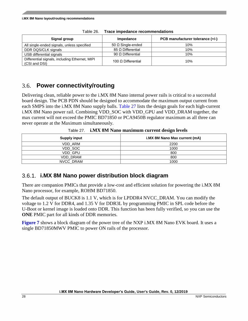
Table 26. Trace impedance recommendations
Signal group Impedance PCB manufacturer tolerance (+/-)
All single-ended signals, unless specified 50 Ω Single-ended 10%
DDR DQS/CLK signals 85 Ω Differential 10%
USB differential signals 90 Ω Differential 10%
Differential signals, including Ethernet, MIPI
(CSI and DSI) 100 Ω Differential 10%
3.6. Power connectivity/routing
Delivering clean, reliable power to the i.MX 8M Nano internal power rails is critical to a successful
board design. The PCB PDN should be designed to accommodate the maximum output current from
each SMPS into the i.MX 8M Nano supply balls. Table 27 lists the design goals for each high-current
i.MX 8M Nano power rail. Combining VDD_SOC with VDD_GPU and VDD_DRAM together, the
max current will not exceed the PMIC BD71850 or PCA9450B regulator maximum as all three can
never operate at the Maximum simultaneously.
Table 27. i.MX 8M Nano maximum current design levels
Supply input i.MX 8M Nano Max current (mA)
VDD_ARM 2200
VDD_SOC 1000
VDD_GPU 800
VDD_DRAM 800
NVCC_DRAM 1000
3.6.1. i.MX 8M Nano power distribution block diagram
There are companion PMICs that provide a low-cost and efficient solution for powering the i.MX 8M
Nano processor, for example, ROHM BD71850.
The default output of BUCK8 is 1.1 V, which is for LPDDR4 NVCC_DRAM. You can modify the
voltage to 1.2 V for DDR4, and 1.35 V for DDR3L by programming PMIC in SPL code before the
U-Boot or kernel image is loaded onto DDR. This function has been fully verified, so you can use the
ONE PMIC part for all kinds of DDR memories.
Figure 7 shows a block diagram of the power tree of the NXP i.MX 8M Nano EVK board. It uses a
single BD71850MWV PMIC to power ON rails of the processor.

i.MX 8M Nano layout/routing recommendations
i.MX 8M Nano Hardware Developer’s Guide, User's Guide, Rev. 0, 12/2019
NXP Semiconductors 29
Figure 7. i.MX 8M Nano development platform power distribution block diagram
3.6.2. Power routing/distribution requirements
The designing for a good Power Delivery Network (PDN) is complicated. It includes:
1. Choose a good PCB stack-up (adequate Cu thicknesses, and layer assignments/utilization).

i.MX 8M Nano layout/routing recommendations
i.MX 8M Nano Hardware Developer’s Guide, User's Guide, Rev. 0, 12/2019
30 NXP Semiconductors
2. Optimize the placement and routing of the PDN. This includes good placement of the decoupling
capacitors and connecting them to the power ground planes with as short and wide a trace as
possible (as the increased inductance of a longer etch will degrade the effectivity of the capacitor).
Use the number/placement of capacitors on the NXP development platforms.
3. Optimize DC IR drop. This involves using very wide traces/plane fills to route high-current power
nets and ensure an adequate number of vias on power net layer transitions. Neck down of fill areas
should be minimized and current density minimized. The maximum DC IR drop on a board should
be 2% (preferably 1%) of the voltage rail (i.e., on a 1.1V rail, the maximum voltage drop should be
less than 0.022 V, preferably less than 0.011 V). See Table 28 for the DC IR drop requirement.
4. AC impedance check – the target impedance at different frequencies should be below specified
values. See Table 29 for the impedance targets vs. frequency for specified power rail for the i.MX
8M Nano PCB design.
Table 28. i.MX 8M Nano DC IR drop requirements
Supply input Nominal
voltage (V)
Max
current (mA) IR drop target
Corresponding power path
resistance requirement (mΩ)
VDD_ARM 0.85/0.95/1.0 2200 <2% <7.7
VDD_SOC&DRAM&GPU 0.85/0.95 2000 <2% <8.5
NVCC_DRAM 1.1 1000 <2% <22
Table 29. i.MX 8M Nano PDN target impedance
Supply Input < 20 MHz (mΩ) 20 - 100 MHz (mΩ)
VDD_ARM 33 154
VDD_SOC&DRAM&GPU 12 58
NVCC_DRAM 17 78
3.7. USB connectivity
The i.MX 8M Nano provides one complete USB2.0 interface and the following configurations (or any
subset) are supported:
• Dedicated host or device using Type-A connector or Type-B connector;
• Dual role using Type-C connector.
To implement a USB Type-C interface (UFP, DFP, or DRP), external hardware must be added to
manage the two configuration channel IOs (CC1 and CC2) as well as monitor the plug orientation.
See the NXP development platform schematic for an example USB Type-C implementation.

Avoiding board bring-up problems
i.MX 8M Nano Hardware Developer’s Guide, User's Guide, Rev. 0, 12/2019
NXP Semiconductors 31
3.8. Unused input/output terminations
3.8.1. i.MX 8M Nano unused input/output guidance
For the i.MX 8M Nano, the I/Os and power rails of an unused function can be terminated to reduce
overall board power. Table 30 lists connectivity examples for unused power supply rails and Table 31
list connectivity examples for unused signal contacts/interfaces.
Table 30. i.MX 8M Nano unused power rail strapping recommendations
Function Ball name Recommendation if unused
MIPI-CSI & MIPI-DSI VDD_MIPI_1P8, VDD_MIPI_1P2, VDD_MIPI_0P8 Leave unconnected1
USB VDD_USB_3P3, VDD_USB_1P8, VDD_USB_0P8 Leave unconnected2
GPU VDD_GPU Leave unconnected
Digital I/O supplies
NVCC_CLK, NVCC_ECSPI, NVDD_ENET,
NVCC_GPIO1, NVCC_I2C, NVCC_JTAG,
NVCC_NAND, NVCC_SAI2, NVCC_SAI3,
NVCC_SAI5, NVCC_SD1, NVCC_SD2, NVCC_UART,
NVCC_SNVS_1P8, PVCC0_1P8, PVCC1_1P8,
PVCC2_1P8
All digital I/O supplies listed in this table must be powered under normal conditions whether the associated I/O pins are in use or not, and associated I/O pins need to enable pull in pad control register to limit any floating gate current.
1. These balls supply both MIPI-CSI and MIPI-DSI interfaces and must be connected/powered if either is used. 2. These balls supply the USB interface(USB1) and must be connected/powered if any USB port is used.
Table 31. i.MX 8M Nano unused signal strapping recommendations
Function Ball name Recommendation if
unused
MIPI-CSI MIPI_CSI_CLK_P/N, MIPI_CSI_Dx_P/N Tie all signals to ground
MIPI-DSI MIPI_DSI_CLK_P/N, MIPI_DSI_Dx_P/N, MIPI_VREG_CAP Leave unconnected
USB1 USB1_VBUS, USB1_DN/DP, USB1_ID, USB1_TXRTUNE Leave unconnected
4. Avoiding board bring-up problems
4.1. Introduction
This chapter describes how to avoid mistakes when bringing up a board for the first time. The
recommendations below consist of basic techniques for detecting board issues and preventing/locating
the three issues encountered: power, clocks, and reset.

Avoiding board bring-up problems
i.MX 8M Nano Hardware Developer’s Guide, User's Guide, Rev. 0, 12/2019
32 NXP Semiconductors
4.2. Avoiding power pitfalls -Current
Excessive current can damage the board. Use a current-limiting laboratory supply set to the expected
main current draw (at most). Monitor the main supply current with an ammeter when powering up the
board for the first time. You can use the supply's internal ammeter if there is. By monitoring the main
supply current and controlling the current limit, any excessive current can be detected before permanent
damage occurs.
Before the board test, you can ohm out the board power rails to the ground to verify that there are no
short circuits. Then, you can power on the board and there will not be any damage to the board and/or
components.
4.3. Avoiding power pitfalls -Voltage
To avoid incorrect voltage rails, create a basic table called a voltage report prior to board bring
up/testing. The table helps to validate that all the supplies are reaching the expected levels.
To create a voltage report, list the following:
• Board voltage sources
• Default power-up values for the board voltage sources
• Best location on the board to measure the voltage level of each supply
Determine the best measurement location for each power supply to avoid a large voltage drop (IR drop)
on the board. The drop causes inaccurate voltage values. The following guidelines help produce the best
voltage measurements:
• Measure closest to the load (in the case of the i.MX 8M Nano processor).
• Make two measurements: the first after initial board power-up and the second while running a
heavy use-case that stresses the i.MX 8M Nano processor.
Ensure that the i.MX 8M Nano power supply meets the DC electrical specifications as listed in the chip-
specific data sheet. See Table 32 for a sample voltage report table.
NOTE
This report table is for the i.MX 8M Nano EVK board. Sample voltage
reports for customer PCBs will be different from this, depending on the
Processor and Power Management IC (PMIC) used and the assignment of
the PMIC power resources.
Table 32. Sample voltage report table
Source Net name Expected (V) Measured (V) Measure point Comment
DC jack input VSYS 5 - TP51 Main supply for
board
BD71850_BUCK1 VDD_SOC&DRAM&PU_0V9 0.85/0.951 - TP22 -
BD71850_BUCK2 VDD_ARM_0V9 0.85/0.95/1.02 - TP23 -
BD71850_BUCK6 VDD_3V3/NVCC_3V3 3.3 - TP25 -
BD71850_BUCK7 VDD_1V8/NVC_1V8 1.8 - TP26 -
BD71850_BUCK8 NVCC_DRAM_1V1 1.1/1.2/1.353 - TP27 -

Avoiding board bring-up problems
i.MX 8M Nano Hardware Developer’s Guide, User's Guide, Rev. 0, 12/2019
NXP Semiconductors 33
1. The default output voltage of BD71850 BUCK1 is 0.8 V. The software will change it to 0.85 V for nominal mode, 0.95V for overdrive mode in SPL before DDR initialization.
2. The default output voltage of BD71850 BUCK2 is 0.9 V. The software will change it to 0.85 V for 1.2 GHz operation, 0.95 V for 1.4 GHz, 1.0 V for 1.5 GHz.
3. 1.1V for LPDDR4, 1.2V for DDR4, 1.35V for DDR3L, BD71850_BUCK8 default output voltage is 1.1V. Software will change it to the required value in SPL before DDR initialization
4.4. Checking for clock pitfalls
Problems with the external clocks are another board bring-up issue. Ensure that all the clock sources are
running as expected.
The 24M_XTALI/24M_XTALO, and the RTC clocks are the main clock sources for 24 MHz and
32.768 kHz reference clocks. Although not required, the use of low jitter external oscillators to feed
CLK1_P/N can be an advantage if low jitter or special frequency clock sources are required by modules
driven by CLKIN_1/2. See the CCM chapter in the i.MX 8M Nano chip reference manual for details.
When checking crystal frequencies, using an active probe is recommended to avoid excessive loading. A
passive probe might inhibit the 24 MHz oscillators from starting up. Use the following guidelines:
• RTC clock is running at 32.768 kHz.
• 24M_XTALI/24M_XTALO is running at 24 MHz (used for the PLL reference).
4.5. Avoiding reset pitfalls
Follow these guidelines to ensure that you are booting correctly.
• During initial power-on while asserting the POR_B reset signal, ensure that 24 MHz and 32.768
kHz clock is active before releasing POR_B.
• Follow the recommended power-up sequence specified in the i.MX 8M Nano data sheet.
• Ensure the POR_B signal remains asserted (low) until all voltage rails associated with bootup are
ON.
The BOOT_MODE[3:0] balls and internal fuses control boot. For a more detailed description about the
boot modes, see the system boot chapter in the chip reference manual.
4.6. Sample board bring-up checklist
The checklist incorporates the recommendations described in the previous sections. Blank cells should
be filled in during the bring-up.
BD71850_LDO1 NVCC_SNVS_1V8 1.8 - TP28 -
BD71850_LDO2 VDD_SNVS_0V8 0.8 - TP29 -
BD71850_LDO3 VDDA_1V8 1.8 - TP32 -
BD71850_LDO6 VDD_PHY_1V2 1.2 - TP31 -
BD71850_MUXSW NVCC_SD2 3.3/1.8 - TP33 Can be either
under SW
control

Avoiding board bring-up problems
i.MX 8M Nano Hardware Developer’s Guide, User's Guide, Rev. 0, 12/2019
34 NXP Semiconductors
Table 33. Board bring-up checklist
Checklist item Details Owner Findings
&Status
Note: The following items must be completed serially.
1. Perform a visual
inspection
Check major components to make sure nothing has been
misplaced or rotated before powering ON.
2. Verify all i.MX 8M Nano voltage rails
Confirm that the voltages match the data sheet’s
requirements. Be sure to check voltages as close to the
i.MX 8M Nano as possible (like on a bypass capacitor). This
reveals any IR drops on the board that could cause issues
later. Ideally, all the i.MX 8M Nano voltage rails should be
checked, but see guidance below for important rails to
check for the i.MX 8M Nano.
VDD_SNVS, NVCC_SNVS, VDD_SOC, VDD_ARM,
VDD_DRAM, NVCC_DRAM are particularly important
voltages, and must fall within the parameters provided in
the i.MX 8M Nano data sheet.
3. Verify power-up sequence
Verify that power on reset (POR_B) is deserted (high) after
all power rails have come up and are stable. See the i.MX
8M Nano data sheet for details about power-up sequencing.
4. Measure/probe input clocks (32.768 kHz, 24
MHz, others)
Without proper clocks, the i.MX 8M Nano will not function
correctly.
5. Check JTAG connectivity
This is one of the most fundamental and basic access
points to the i.MX 8M Nano to allow the debug and
execution of low level code, and probe/access processor
memory.
Note: The following items may be worked on in parallel with other bring-up tasks.
Access internal RAM
Verify basic operation of the i.MX 8M Nano in system. The
on-chip internal RAM starts at address 0x0090 0000 and is
128 Kbytes in density. Perform a basic test by performing a
write-read-verify operation to the internal RAM. No software
initialization is required to access internal RAM.
Verify CLKO outputs (measure
and verify default clock
frequencies for desired clock
output options) if the board design
supports the probing of clock
output balls.
This ensures that the corresponding clock is working and
that the PLLs are working. This step requires chip
initialization, for example, via the JTAG debugger, to
properly set up the IOMUX to output clocks to I/O balls and
to set up the clock control module to output the desired
clock. See the chip reference manual for more details.
Measure boot mode
frequencies. Set the boot
configure switch for each boot
mode and measure the following
(depending on system
availability):
• NAND (probe CE to verify
boot, measure RE frequency)
• SPI-NOR (probe slave select
and measure clock
frequency)
• MMC/SD (measure clock
frequency)
This verifies the connectivity of signals between the i.MX
8M Nano and boot device and that the boot mode signals
are properly set. See the “System Boot” chapter in the chip
reference manual for details for boot mode configurations.
Run basic DDR initialization and
test memory 1. Assuming the use of a JTAG debugger, run the
DDR initialization and open a debugger memory

Using BSDL for Board-level Testing
i.MX 8M Nano Hardware Developer’s Guide, User's Guide, Rev. 0, 12/2019
NXP Semiconductors 35
Table 33. Board bring-up checklist
Checklist item Details Owner Findings
&Status
window pointing to the DDR memory map starting address.
2. Try writing a few words and verify if they can be read correctly.
3. If not, recheck the DDR initialization sequence and whether the DDR has been correctly soldered onto the board. Users should recheck the schematic to ensure that the DDR memory has been connected to the i.MX 8M Nano correctly.
5. Using BSDL for Board-level Testing
5.1. BSDL overview
Boundary scan description language (BSDL) is used for board-level testing after components have been
assembled. The interface for this test uses the JTAG pins. The definition is contained within IEEE Std
1149.1.
5.2. How BSDL functions
A BSDL file defines the internal scan chain, which is the serial linkage of the IO cells, within a
particular device. The scan chain looks like a large shift register, which provides a means to read the
logic level applied to a pin or to output a logic state on that pin. Using JTAG commands, a test tool uses
the BSDL file to control the scan chain so that device-board connectivity can be tested.
For example, when using an external ROM test interface, the test tool would do the following:
1. Output a specific set of addresses and controls to pins connected to the ROM
2. Perform a read command and scan out the values of the ROM data pins.
3. Compare the values read with the known golden values.
Based on this procedure, the tool can determine whether the interface between the two parts is connected
properly and does not contain shorts or opens.
5.3. Downloading the BSDL file
The BSDL file for each i.MX processor is stored on the NXP website upon product release. Contact
your local sales office or fields applications engineer to check the availability of information prior to
product releases.

Using BSDL for Board-level Testing
i.MX 8M Nano Hardware Developer’s Guide, User's Guide, Rev. 0, 12/2019
36 NXP Semiconductors
5.4. Pin coverage of BSDL
Each pin is defined as a port within the BSDL file. You can open the file with a text editor (like
Wordpad) to review how each pin will function. The BSDL file defines these functions as shown:
-- PORT DESCRIPTION TERMS
-- in = input only
-- out = three-state output (0, Z, 1)
-- buffer = two-state output (0, 1)
-- inout = bidirectional
-- linkage = OTHER (vdd, vss, analog)
The appearance of ”linkage” in a pin’s file implies that the pin cannot be used with boundary scan.
These are usually power pins or analog pins that cannot be defined with a digital logic state.
5.5. Boundary scan operation
When using the BSDL file to force the i.MX8M Nano enter the boundary scan mode on the EVK board,
it needs a special setup sequence as below:
• BOOT_MODE0(G26)&BOOT_MODE1(G27)& BOOT_MODE2(C27)& BOOT_MODE3(D26)
should be high, set the SWITCH SW1101[1-4]: 1111, then power up the board.
• Load the instruction and data codes to the chip TAP controller by JTAG port to enter boundary-
scan mode.
o Soft reset the JTAG TAP controller, go to Test-Logic Reset state.
o Go to Shift-IR state, load IR Instruction = b10000.
o Go to RUN-TEST-IDLE sate.
o Go to Shift-DR state, load DR data = b00111000
o Go to RUN-TEST-IDLE state
o End task.
Refer to Figure 8 for the TAP controller state, TMS is used to determine the next state of the
TAP controller, the serial instructions and data are received by the test logic at TDI. The value
shown adjacent to each state transition in this figure represents the signal present at TMS at the
time of a rising edge at TCK.

Using BSDL for Board-level Testing
i.MX 8M Nano Hardware Developer’s Guide, User's Guide, Rev. 0, 12/2019
NXP Semiconductors 37
Figure 8. TAP controller state diagram
NOTE
1. GPIO1_IO02 is used as WDOG_B to toggle the PMIC. When entering
boundary-scan mode, this pin is always low which will repeatedly
reset the PMIC and prevent the system boot up normally. So the PMIC
WDOG_B pin can’t be connected to GPIO1_IO02 and should be
pulled up to 100Kohm resistor during boundary scan test. Or use the
WDOG timer buffer circuit as below.
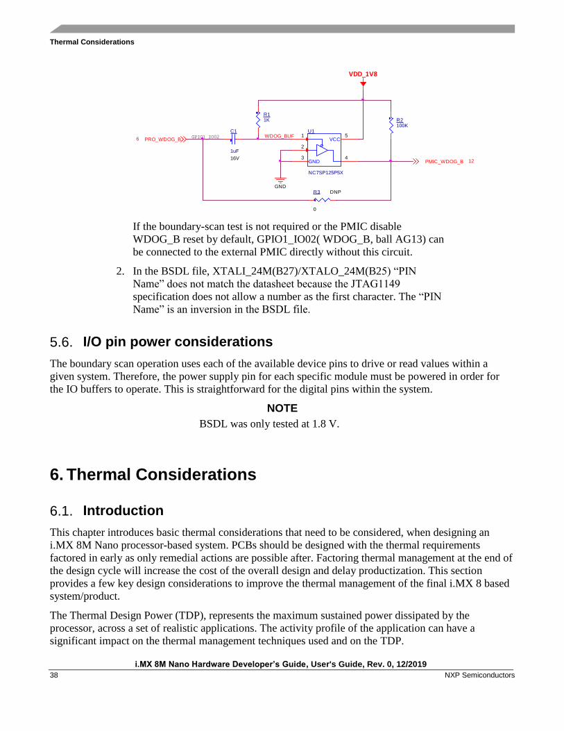
Thermal Considerations
i.MX 8M Nano Hardware Developer’s Guide, User's Guide, Rev. 0, 12/2019
38 NXP Semiconductors
R2100K
GND
PRO_WDOG_B6
R3
0
DNP
PMIC_WDOG_B 12
R11K
WDOG_BUF
VDD_1V8
GPIO1_IO02
C1
1uF
16V
VCC
GND
U1
NC7SP125P5X
1
2
3 4
5
If the boundary-scan test is not required or the PMIC disable
WDOG_B reset by default, GPIO1_IO02( WDOG_B, ball AG13) can
be connected to the external PMIC directly without this circuit.
2. In the BSDL file, XTALI_24M(B27)/XTALO_24M(B25) “PIN
Name” does not match the datasheet because the JTAG1149
specification does not allow a number as the first character. The “PIN
Name” is an inversion in the BSDL file.
5.6. I/O pin power considerations
The boundary scan operation uses each of the available device pins to drive or read values within a
given system. Therefore, the power supply pin for each specific module must be powered in order for
the IO buffers to operate. This is straightforward for the digital pins within the system.
NOTE
BSDL was only tested at 1.8 V.
6. Thermal Considerations
6.1. Introduction
This chapter introduces basic thermal considerations that need to be considered, when designing an
i.MX 8M Nano processor-based system. PCBs should be designed with the thermal requirements
factored in early as only remedial actions are possible after. Factoring thermal management at the end of
the design cycle will increase the cost of the overall design and delay productization. This section
provides a few key design considerations to improve the thermal management of the final i.MX 8 based
system/product.
The Thermal Design Power (TDP), represents the maximum sustained power dissipated by the
processor, across a set of realistic applications. The activity profile of the application can have a
significant impact on the thermal management techniques used and on the TDP.

Thermal Considerations
i.MX 8M Nano Hardware Developer’s Guide, User's Guide, Rev. 0, 12/2019
NXP Semiconductors 39
If the customer application requires high performance for extended periods and/or if the product is
required to function in high ambient temperatures, the usage of passive thermal management techniques
such as a heatsink becomes necessary. For very high ambient operating environments active thermal
management techniques such a cooling fan or forced convection may also be required in addition to the
heatsink.
For most of the applications it may be feasible to consider the PCB as the only heat dissipation media,
providing that good design practices are followed.
6.2. PCB Dimensions
The dimensions of the PCB directly affect its capability to dissipate the heat. Typically, more than 80%
of the heat generated by a high-power component is dissipated through the system board, when no other
thermal solution is implemented. The bigger the board is, the larger the surface area through which heat
can spread away from the source component and also can be transferred more efficiently into free space.
NXP conducted PCB sensitivity simulation showed that a 50% reduction in PCB x-y dimensions results
in an increase of between 44-65% in package thermal resistance due to the loss in conductive volume to
dissipate heat. System designers hence need to be careful when designing smaller form factor boards
that have multiple high-power components.
6.3. Copper Volume
Increasing the heat dissipation (reducing thermal resistance) can also be achieved by increasing the
metallization in the system board. PCBs are made up of copper and dielectric material, with the copper
being orders of magnitude more thermally conductive. Copper volume influences the heat capacity of
the board. With higher copper volume the board can accept more heat, so a i.MX 8 processor-based
system can operate in high performance state (or near the max TDP) for longer time periods. The copper
volume can be increased by increasing the dimensions of the board, by addition of ground layers or by
increasing the thicknesses of the layers on which power and ground planes are located. Please refer to
Table 19 and Table 20 for stack-up of the EVK.
6.3.1. PCB Material Selection
As previously discussed PCB material selection is extremely important for systems with high speed
routing. Thermal properties should also be considered in selecting PCB materials for multilayer designs
in which the system is expected to endure excessive short-term thermal steps. Specific attention should
be paid to the fact that thermal properties of dielectrics are often different in horizontal and vertical
directions.
Material characteristics such as the Coefficient of Thermal Expansion (CTE) should be considered. The
CTE describes how a material changes dimension with temperature. Ideally, a PCB material’s CTE
should be closely matched to copper, which is about 17 ppm°C. CTE is a concern because as the PCB
expands during heating, it can elongate plated via holes and cause fracturing. If the CTE is closely
matched to copper, expansion of the PCB material and copper will be more uniform and the plated via
holes will be more robust during thermal cycling.

Thermal Considerations
i.MX 8M Nano Hardware Developer’s Guide, User's Guide, Rev. 0, 12/2019
40 NXP Semiconductors
6.4. Thermal Resistance
Reducing the thermal resistance close to the die and package is mandatory for good thermal
performance. The actual semiconductor die dimensions are relatively small compared to the size of a
typical PCB, which results in a very high heat flux in the die, package and its immediate vicinity.
Therefore, thermal resistance encountered early in the thermal path causes a large temperature gradient.
The most effective place to focus resources to reduce thermal resistance is where the thermal gradient is
the highest. To efficiently dissipate the heat through the board, thermal resistance between the SoC and
the board needs to be minimized. This can be achieved by utilizing all the ground pads of the component
and using underfill with good thermal conductivity properties.
6.4.1. Heat Spreaders
Thermal resistance can be reduced when a heat spreader is mounted on the top of SoC package using a
Thermal Interface Material (TIM) with good thermal conductivity properties (thermal paste). If the heat
spreader is also thermally connected with the PCB, an alternative route for the heat is created, reducing
the global thermal resistance. Spreading the heat at the beginning of the thermal path not only reduces
the thermal resistance near the source component, but it also provides a broader area to further
disseminate the heat.
The type of heat spreader to be used is dependent on the customers’ application available enclosure
space and budget considerations. Graphite heat spreaders are quite common as they match the thermal
performance of copper in two directions (x, y), at a lower weight and cost. The high in-plane (basal)
thermal conductivity results in spreading and evening out of the hot spots Due its low cost the area that
the graphite heat spreader covers, could be potentially larger covering all heat generating components on
the system board.
6.4.2. Thermal Vias
Using a continuous low thermal impedance path from the processor to ambient conditions is important
and a low thermal resistance has to be maintained throughout the PCB. Any small break in the low
impedance path is highly detrimental. System designers should provide redundant thermal paths where
possible. This can be achieved by adding an appropriate amount of thermal vias to connect all the
ground planes together and allow the heat to spread uniformly through other layers of the PCB. System
designers should allocate enough plated through vias around the ground and power balls of the i.MX
processor and other heat generating components.
6.5. Power Net Design
Modern power electronics devices can have very low on-resistances. It’s quite possible that the PCB
traces and connector pins that feed current to these devices contribute more ohmic losses to the system
than the power transistors do. Such heating may be avoidable if traces are up-sized. Reducing trace
ohmic losses may be the least expensive way to reduce the design's total power dissipation. Trace width
calculators, which also predict trace temperature rise, are readily available on the internet. Using over-
sized power transistors is a way to cut total power and subsequent heat dissipation.
Thermal Considerations
i.MX 8M Nano Hardware Developer’s Guide, User's Guide, Rev. 0, 12/2019
NXP Semiconductors 41
6.6. Component Placement
The i.MX 8 processor should always be placed away from edges in the center of the PCB so that heat
can effectively spread in all directions. Placing the device on the edge or even on the corner of the PCB
significantly reduces heat transfer from the device and dissipation capabilities of the to the PCB, as the
heat cannot efficiently spread in the directions where the edges are present. This eventually results in
local hot spots and rapid heating of the source component.
In addition, the processor should be mounted on the top side of the PCB, away from the chassis walls.
System designers should place heat generating components as far apart as possible to reduce thermal
coupling effects. The thermal gradient is high near a power dissipating device, so even small amounts of
separation help reduce thermal coupling.
A NXP conducted PCB sensitivity simulation showed that a non-centered bare i.MX 8 FCBGA package
on the PCB will cause approximately 8-10% increase in junction temperature due to uneven heat
propagation. This study highlights the need for centered component placement.
6.7. PCB Surroundings
The surroundings of the PCB also influence the efficiency of heat transfer from the board into free space
(air). There should be enough clearance from the top and bottom sides of the PCB. If narrow gaps are
created, air flow is significantly limited, resulting in accumulation of hot air in the gap. The board
cannot therefore effectively transfer heat in such areas. Also, the casing should be designed in a way that
natural air convection could be utilized to improve heat transfer.
If a narrow gap at the bottom side cannot be avoided (quite common for System on Modules - SOMs), it
should be considered to fill the gap under the i.MX processor by thermally conductive gap filler. To
further improve heat transfer, exposed copper pads should be added to the base board at the mounting
spot of the filler.
6.7.1. Air Flow Considerations
Heat convection is more efficient for a vertically mounted board. Remember that components above
heat producing devices run hotter than those below. If the board is to be horizontally mounted, place
heat generating components on the PCB’s topside, if possible. A thermal plume (the chimney effect)
forms more readily on a board’s topside and it helps disperse heat.
• Consider the system level air flow and air mover placement in the enclosure
• Avoid sub-optimal component placement that might hinder airflow or natural convection
• Avoid placing tall or bulky devices in the air flow path
• Avoid routing circuitry in an area where mounting holes would need to go
• Plan to make space for the thermal management solution early in the system design phase and
consider the complete board and packaging form factor (enclosure)
Thermal Considerations
i.MX 8M Nano Hardware Developer’s Guide, User's Guide, Rev. 0, 12/2019
42 NXP Semiconductors
6.8. Thermal Simulations
As illustrated in this section, thermal management is a very complex discipline with numerous variables
that need to be considered. In order to determine whether the system is capable of stable operation (no
thermal runaways) in the given use case or to identify potentially overlooked issues, thermal simulations
have to be performed.
NXP can provide FloTHERM simulation models for i.MX 8 series processor family and strongly
encourages customers to perform thermal simulations using these models in their form factor designs
and specific use cases to get a holistic system thermal design & identify possible thermal bottlenecks.
Thermal simulations become increasingly important in small form factor designs and operation in high
ambient temperatures.
6.9. Software optimization
Software based power and thermal management techniques can be very effective in reducing the need
for more elaborate active or passive thermal management solutions and add little or no additional cost to
the system design. Attention should be paid to the required system performance and power
requirements, as lower the i.MX 8 processor power consumption lower the heat generated by the
processor.
The i.MX 8 series incorporates several low-power design techniques, to meet requirements of low-
power design, while sustaining high performance operation. The activity profile of the customer
application can have a significant impact on the thermal management techniques used and on the TDP.
Carefully defining the system’s worst case operating conditions can be an effective way to reduce power
and thermal dissipation.
• System designers should utilize and enable all software power management techniques available
for the i.MX 8 Series
• The SoC voltages and core frequencies of modules should be kept at the minimum specified
levels and scaled dynamically with respect to the current performance demands of the
application where possible
• The processor should enter low power modes under certain use cases whenever possible
• All unused power rails should be turned off from the PMIC and power gate unused domains if
possible
• All unused module clocks should be turned off (Dynamically handled by NXP Linux BSP)
• Customers are encouraged to use the latest Linux BSP GA release available on nxp.com, that
leverages the i.MX 8 processor power management features and incorporates various Linux
software power management techniques
6.10. The Thermal Checklist
NXP recommends using the checklist below as a high-level guide for designing an optimal thermal
management solution for your end product:

Revision history
i.MX 8M Nano Hardware Developer’s Guide, User's Guide, Rev. 0, 12/2019
NXP Semiconductors 43
Table 34. Thermal checklist
Item Activity Check
1 Determine the TDP (Thermal Design Power)
2 Determine the Activity Profile (use case dependent)
3 Determine the product form factor constraints (orientation, x, y & z limits etc.)
4 Determine the environmental operating conditions (ambient temperature, airflow regime -
Forced or Natural Convection)
5 Determine the Tj for the i.MX 8 device to use (Auto, Industrial, consumer, package lidded
etc.)
6 Factor in board design considerations early (PCB layers, metallization, layout, component
placement)
7 Run thermal simulations to determine the best thermal management approach using form
factor design and use cases
8 Investigate adding heat spreading techniques, heatsinks to alleviate thermal bottlenecks
9 Enable all software power management techniques which can minimize power
consumption (less power, less heat)
10 Consider lower power memory and other system components, or retarget use case
7. Revision history Table 35. Revision history
Revision number Date Substantive changes
0 12/2019 Initial release

Document Number: IMX8MNHDG Rev. 0
12/2019
How to Reach Us:
Home Page:
nxp.com
Web Support:
nxp.com/support
Information in this document is provided solely to enable system and software implementers
to use NXP products. There are no express or implied copyright licenses granted hereunder to
design or fabricate any integrated circuits based on the information in this document. NXP
reserves the right to make changes without further notice to any products herein.
NXP makes no warranty, representation, or guarantee regarding the suitability of its products
for any particular purpose, nor does NXP assume any liability arising out of the application or
use of any product or circuit, and specifically disclaims any and all liability, including without
limitation consequential or incidental damages. “Typical” parameters that may be provided in
NXP data sheets and/or specifications can and do vary in different applications, and actual
performance may vary over time. All operating parameters, including “typicals,” must be
validated for each customer application by customer's technical experts. NXP does not convey
any license under its patent rights nor the rights of others. NXP sells products pursuant to
standard terms and conditions of sale, which can be found at the following address:
nxp.com/SalesTermsandConditions.
While NXP has implemented advanced security features, all products may be subject to
unidentified vulnerabilities. Customers are responsible for the design and operation of their
applications and products to reduce the effect of these vulnerabilities on customer’s
applications and products, and NXP accepts no liability for any vulnerability that is discovered.
Customers should implement appropriate design and operating safeguards to minimize the
risks associated with their applications and products.
NXP, NXP, the NXP logo, NXP SECURE CONNECTIONS FOR A SMARTER WORLD,
COOLFLUX, EMBRACE, GREENCHIP, HITAG, I2C BUS, ICODE, JCOP, LIFE VIBES,
MIFARE, MIFARE CLASSIC, MIFARE DESFire, MIFARE PLUS, MIFARE FLEX, MANTIS,
MIFARE ULTRALIGHT, MIFARE4MOBILE, MIGLO, NTAG, ROADLINK, SMARTLX,
SMARTMX, STARPLUG, TOPFET, TRENCHMOS, UCODE, Freescale, the Freescale logo,
AltiVec, C-5, CodeTEST, CodeWarrior, ColdFire, ColdFire+, C-Ware, the Energy Efficient
Solutions logo, Kinetis, Layerscape, MagniV, mobileGT, PEG, PowerQUICC, Processor
Expert, QorIQ, QorIQ Qonverge, Ready Play, SafeAssure, the SafeAssure logo, StarCore,
Symphony, VortiQa, Vybrid, Airfast, BeeKit, BeeStack, CoreNet, Flexis, MXC, Platform in a
Package, QUICC Engine, SMARTMOS, Tower, TurboLink, and UMEMS,EdgeScale,
EdgeLock, eIQ, and Immersive 3D are trademarks of NXP B.V. All other product or service
names are the property of their respective owners. Arm, AMBA, Arm Powered, Artisan,
Cortex, Jazelle, Keil, SecurCore, Thumb, TrustZone, and μVision are registered trademarks of
Arm Limited (or its subsidiaries) in the EU and/or elsewhere. Arm7, Arm9, Arm11, big.LITTLE,
CoreLink, CoreSight, DesignStart, Mali, Mbed, NEON, POP, Sensinode, Socrates, ULINK and
Versatile are trademarks of Arm Limited (or its subsidiaries) in the EU and/or elsewhere. All
rights reserved. Oracle and Java are registered trademarks of Oracle and/or its affiliates. The
Power Architecture and Power.org word marks and the Power and Power.org logos and
related marks are trademarks and service marks licensed by Power.org.
© 2019 NXP B.V.