![Improving Smart Conference Participation through Socially-Aware …thealphalab.org/papers/THMS-13-11-0364-FinalVersion.pdf · 2016. 10. 17. · Based Filtering (CBF) [7] and Hybrid](https://static.fdocuments.us/doc/165x107/60f81b19fbfe56776659d38b/improving-smart-conference-participation-through-socially-aware-2016-10-17.jpg)
ImprovingtheBreakdownVoltage,ON–resistance and Gate...
13
Improving the Breakdown Voltage, ON–resistance and Gate–charge of InGaAs LDMOS Power Transistors M. Jagadesh Kumar and Avikal Bansal Department of Electrical Engineering, Indian Institute of Technology Delhi, New Delhi – 110 016, India E-mail: [email protected] Abstract. Recently, a lateral double diffused metal-oxide-semiconductor (LDMOS) using In 0.53 Ga 0.47 As having an extended–p + (ep + ) body has been shown to be better than a conventional silicon based LDMOS. In this paper, we show that using a stepped gate (SG) for the InGaAs LDMOS, a significantly improved performance can be achieved than using an extended–p + body for the InGaAs LDMOS. The proposed device has three steps with the gate oxide thickness increasing from the source to the drain. The stepped gate oxide has the following advantages: a good gate control is achieved because of the smaller oxide thickness near the source, lesser gate to drain capacitance is possible due to the greater oxide thickness near the drain and the ON– resistance decreases as a consequence of increased drift region doping which is possible due to the increased thickness of the gate oxide over the drift region. The large mobility of electrons in InGaAs also enhances the current flow and reduces the ON–resistance. Based on 2-D device simulation results, we show that the SG LDMOS using InGaAs exhibits 49.7 % improvement in the breakdown voltage, 43.8 % improvement in ON– resistance, 105.0 % improvement in the range of transconductance, 33.6 % improvement in gate charge and 60.1 % improvement in switching speed as compared to an LDMOS using InGaAS with buried–p + body. PACS numbers: 73.40.Qv, 85.30.Tv Submitted to: Semicond. Sci. Technol.
Transcript of ImprovingtheBreakdownVoltage,ON–resistance and Gate...
Improving the Breakdown Voltage, ON–resistance
and Gate–charge of InGaAs LDMOS Power
Transistors
M. Jagadesh Kumar and Avikal Bansal
Department of Electrical Engineering, Indian Institute of Technology Delhi, New
Delhi – 110 016, India
E-mail: [email protected]
Abstract. Recently, a lateral double diffused metal-oxide-semiconductor (LDMOS)
using In0.53Ga0.47As having an extended–p+ (ep+) body has been shown to be better
than a conventional silicon based LDMOS. In this paper, we show that using a stepped
gate (SG) for the InGaAs LDMOS, a significantly improved performance can be
achieved than using an extended–p+ body for the InGaAs LDMOS. The proposed
device has three steps with the gate oxide thickness increasing from the source to the
drain. The stepped gate oxide has the following advantages: a good gate control is
achieved because of the smaller oxide thickness near the source, lesser gate to drain
capacitance is possible due to the greater oxide thickness near the drain and the ON–
resistance decreases as a consequence of increased drift region doping which is possible
due to the increased thickness of the gate oxide over the drift region. The large mobility
of electrons in InGaAs also enhances the current flow and reduces the ON–resistance.
Based on 2-D device simulation results, we show that the SG LDMOS using InGaAs
exhibits 49.7 % improvement in the breakdown voltage, 43.8 % improvement in ON–
resistance, 105.0 % improvement in the range of transconductance, 33.6 % improvement
in gate charge and 60.1 % improvement in switching speed as compared to an LDMOS
using InGaAS with buried–p+ body.
PACS numbers: 73.40.Qv, 85.30.Tv
Submitted to: Semicond. Sci. Technol.
M.Jagdish
Text Box
Semiconductor Science and Technology, Vol.27, No.10, Article No.105030, October 2012.
Improving InGaAs LDMOS Power Transistors 2
1. Introduction
Silicon and GaAs are widely used for power MOSFET devices. Silicon is used because of
its ease of fabrication with CMOS process. GaAs devices are used in cellular handsets,
optoelectronics and monolithic microwave integrated circuits. The principal requirement
for the devices used in RF applications is lower ON–resistance, lower gate capacitance
and higher transconductance [1]. Various techniques have been implemented to improve
the characteristics of the power MOSFETs [2, 3, 4, 5, 6, 7]. A trade-off needs to be
achieved among the performance parameters of an LDMOS. If we improve the speed by
reducing the gate capacitance, the gate control deteriorates and the transconductance is
degraded. Similarly, if we improve the breakdown voltage, the ON–resistance increases.
With silicon reaching its performance limit, we need to explore new materials for
enhancing the performance of LDMOS. InGaAs is a new material with higher mobility
compared to silicon. The major problem for III-V materials is the absence of native
oxide like SiO2 for silicon. The integration of high–κ gate oxides on InGaAs with lesser
fixed oxide charge density is the major obstacle in the development of these devices
[8, 9, 10, 11]. With the improvements in the fabrication process, the oxide–InGaAs
interface is improved [8, 9]. InGaAs nanoscale MOSFETs have shown to have better
performance compared to silicon MOSFETs for low voltage applications [11, 12].
Use of InGaAs in LDMOS was first reported by Steighner et al. [13]. They
reported that the performance of InGaAs device is better as compared to its silicon
counterpart. Extended–p+ body, originally reported in [4] for SOI MOSFETs, was
implemented in InGaAs LDMOS and the on–state breakdown was shown to improve
by its use [13]. In this paper, we propose a stepped gate [3] structure for LDMOS using
In0.53Ga0.47As material. The stepped gate structure increases the transconductance by
reducing the gate oxide thickness near the source and decreases the capacitive coupling
near the drain due to the thicker gate oxide. It also helps in redistributing the electric
field in the channel and the drift region, hence increasing the breakdown voltage [3].
It allows the use of higher drift region doping and therefore, helps in decreasing the
ON–resistance. Thus, with the stepped gate structure, the safe operating area (SOA)
will increase along with the reduction in the ON–resistance.
2. Device Structure and Simulation Parameters
The cross-sections of the proposed device and the reference device [13] are shown in
Figure 1. P–type InP is used as the substrate and In0.53Ga0.47As film is used as
the active material. High–κ dielectric material Al2O3 is used as the gate oxide. The
reference device has an extended–p+ region below the source region to reduce the effect
of parasitic BJT in LDMOS [4]. The SG LDMOS’s gate has three steps with the gate
oxide thickness increasing from the source to the drain. The steps in the gate are all
connected together to form a single gate. The stepped gate helps in redistributing the
electric field and increasing the breakdown voltage of the device [3].

Improving InGaAs LDMOS Power Transistors 3
n-drift regionp
n+
DrainSource
Gate
p+
p-InP substrate
In0.53Ga0.47As
LG1
Tox1
0.0
0.5
1.0
0.0 1.0 2.0 3.0 4.0 5.0 6.0
1.5
n-drift regionp
DrainSource
Gate
p-InP substrate
In0.53Ga0.47As
LG1 LG2 LG3
WSP1 WSP2
Tox1 Tox2 Tox3
0.0 1.0 2.0 3.0 4.0 5.0 6.0
~~
(a)
(b)
p+
n+
n+ n+
Al2O3 Metal
~~ ~~ ~~
~~ ~~
µm
0.0
0.5
1.0
1.5
µm
Figure 1. Cross sectional view of (a) The reference device – ep+ LDMOS [13] and
(b) The proposed device – SG LDMOS.
The fixed oxide charge density is taken as 1.3× 1012 cm−2 [8, 9] . Work function of
the metal for the gate material is chosen to be 4.7 eV . Both the devices, SG LDMOS
and ep+ LDMOS, have approximately the same threshold voltage of 0.5 V . The doping
value for the drift region and the oxide thickness for the second step and the third step
of the gate are optimized to obtain the highest breakdown voltage. The fabrication steps
for the stepped gate structure could be similar to that discussed in [3]. The simulation
parameters of both the devices are listed in Table 1.
3. Simulation Results and Discussion
SG LDMOS and ep+ LDMOS are created and simulated using Silvaco’s 2D device
simulator ATLAS [14]. Appropriate models are invoked for Shokley-Read-Hall
generation and recombination, electric field dependent mobility and selberherr impact
ionization [14]. The electron mobility in InGaAs is calibrated to 5200 cm2V −1s−1 [15].
The energy bandgap at 300 K and the dielectric constant of Al2O3 are taken as 9.0 eV
and 9, respectively. To validate the choice of the models and their parameters used in
Improving InGaAs LDMOS Power Transistors 4
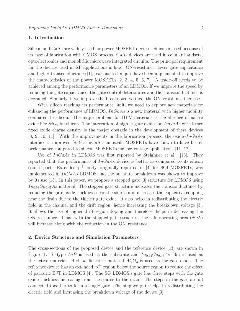
Table 1. Simulation Parameters
Parameter Value
ep+ LDMOS[13] SG LDMOS
TOX1 30 nm 30 nm
TOX2 200 nm
TOX3 400 nm
LG1 2.0 µm 1.0 µm
LG2 350 nm
LG3 350 nm
WSP1 100 nm
WSP2 200 nm
Drift Doping 1× 10¹⁶ /cm3 4× 10¹⁶ /cm3
Channel Doping 3× 10¹⁷ /cm3
Source and Drain
Doping 1× 10¹⁹ /cm3
Channel Length 0.5 µm
Drift Region Length 2.5 µm
In0.53Ga0.47As
Layer Thickness 0.8 µm
Threshold Voltage, VT ≈ 0.5 V
our simulations, we first simulated the LDMOS structure [13] and calculated snapback
curves, output characteristics and gate charge characteristics. Our results were matched
with the ones simulated by Steighner et al., reported and shown in Fig. 2 to Fig. 9 of
[13], with the fixed oxide charge density of 5 × 10¹¹ /cm2 as reported in [13]. However,
in this study, both for the SG LDMOS and ep+ LDMOS, we have chosen the recently
reported value for the fixed oxide charge density viz. 1.3 × 10¹² /cm2 [8, 9].
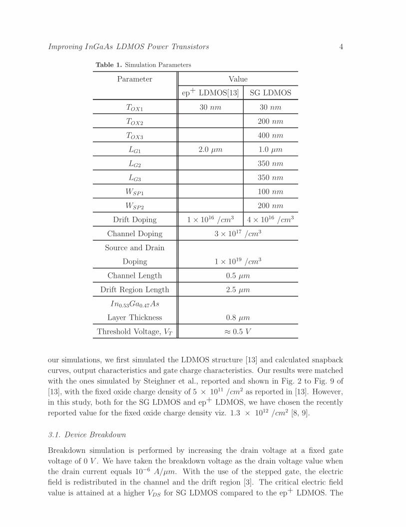
3.1. Device Breakdown
Breakdown simulation is performed by increasing the drain voltage at a fixed gate
voltage of 0 V . We have taken the breakdown voltage as the drain voltage value when
the drain current equals 10−6 A/µm. With the use of the stepped gate, the electric
field is redistributed in the channel and the drift region [3]. The critical electric field
value is attained at a higher VDS for SG LDMOS compared to the ep+ LDMOS. The
Improving InGaAs LDMOS Power Transistors 5
0 10 20 30 40 50 60 7010
−9
10−8
10−7
10−6
10−5
10−4
10−3
10−2
Drain Voltage, VDS
(V)
Dra
in C
urre
nt, I
D (
A/µ
m)
44 V 66 V
SG LDMOS eP+ LDMOS
Figure 2. Breakdown ID − VDS characteristics at VGS = 0 V for SG LDMOS and
ep+ LDMOS.
1.5 2 2.5 3 3.5 4 4.50
0.1
0.2
0.3
0.4
0.5
Lateral Distance, (µm)
Ele
ctric
Fie
ld, (
MV
/cm
)
VDS
= 66 V
VDS
= 44 V
SG LDMOS
eP+ LDMOS
Figure 3. Electric field distribution along the gate oxide and InGaAs interface of the
SG LDMOS and the ep+ LDMOS at the breakdown voltage.
electric field is uniformly distributed in the whole of the drift region for SG LDMOS
as compared to ep+ LDMOS where, it has a higher value towards the drain side of
the drift region compared to the channel side as shown in Figure 3. Therefore, the
breakdown is delayed for the SG LDMOS. The SG LDMOS exhibits a 49.7 % increase
in the breakdown voltage as compared to the ep+ LDMOS as shown in Figure 2.
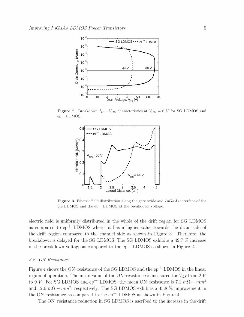
3.2. ON Resistance
Figure 4 shows the ON–resistance of the SG LDMOS and the ep+ LDMOS in the linear
region of operation. The mean value of the ON–resistance is measured for VGS from 2 V
to 9 V . For SG LDMOS and ep+ LDMOS, the mean ON–resistance is 7.1 mΩ−mm2
and 12.6 mΩ−mm2, respectively. The SG LDMOS exhibits a 43.8 % improvement in
the ON–resistance as compared to the ep+ LDMOS as shown in Figure 4.
The ON–resistance reduction in SG LDMOS is ascribed to the increase in the drift

Improving InGaAs LDMOS Power Transistors 6
1 2 3 4 5 6 7 8 95
10
15
20
Gate Voltage, VGS
(V)
ON
−R
esis
tanc
e, R
ON
(m
Ω−
mm
2 )
SG LDMOS
eP+ LDMOS
Figure 4. ON-resistance versus gate voltage at VDS = 0.5 V .
0 2 4 6
30
40
50
60
70
Bre
akdo
wn
Vol
tage
, (V
)
Drift Doping, (× 1016 cm−3)
SG LDMOS ep+ LDMOS
Figure 5. Breakdown voltage dependence on n–drift region doping for SG LDMOS
and ep+ LDMOS
region doping of the SG LDMOS. The maxima for breakdown voltage in SG LDMOS
structure is at a higher value of drift region doping as compared to that of ep+ LDMOS
as shown in Figure 5. Thus, a higher drift region doping results in the lower ON-
resistance.
3.3. Transconductance
Figure 6 shows the transconductance versus VGS for a constant VDS in the saturation
region. We observe that the SG LDMOS exhibits a 105.0 % increase in the range
of gate voltage for which the device responds as compared to the ep+ LDMOS.
Thus, SG LDMOS can be used for greater input voltage range as compared to the
ep+ LDMOS. As shown in Figure 7, the LDMOS consists of a series combination of
an enhancement type MOSFET (M1), a bulk resistor (R2) and a parallel combination
of a depletion type MOSFET (M2) and a bulk resistor (R1) [16]. The enhancement

Improving InGaAs LDMOS Power Transistors 7
0 1 2 3 40
40
80
120
160
200
Tra
nsco
nduc
tanc
e, g
m (
µS/µ
m)
Gate Voltage, VGS
(V)
SG LDMOS ep+ LDMOS
Figure 6. Transconductance as a function of gate voltage for VDS = 4.0 V .
n-driftp-well
DrainSource Gate
n+ n+p+
Substrate
region
M1 M2
R1
R2
Figure 7. Equivalent circuit diagram of an LDMOS[16].
0 1 2 3 40.2
0.3
0.4
0.5
0.6
0.7
Gate Voltage, VGS
(V)
VD
S o
f the
mai
n M
OS
FE
T (
V)
SG LDMOS ep+ LDMOS
Figure 8. Drain potential variation of the main MOSFET versus gate voltage at
VDS = 4.0 V .
type MOSFET (M1) is referred as the main MOSFET of an LDMOS. Figure 8 shows
the potential at the drift region edge near the p–channel and the n–drift junction. The
VDS of the main MOSFET of SG LDMOS remains high for a greater range of VGS
compared to ep+ LDMOS. At a higher gate voltage, the drain current increases and
the potential drop across the bulk resistors increases causing a reduction in the drain
Improving InGaAs LDMOS Power Transistors 8
voltage of the main MOSFET. When VDS of the main MOSFET is higher, LDMOS
operates in the saturation region and for lower VDS, it operates in the linear region.
The transconductance falls for higher VGS because of the linear region of operation of
the main MOSFET [1] forcing the LDMOS to operate in quasi–saturation. Increase in
the drift region doping, decreases the bulk resistance hence, potential drop across the
bulk resistors reduces. Therefore, VDS of the main MOSFET remains high for greater
range of VGS for SG LDMOS compared to the ep+ LDMOS and hence, the input
operating voltage range increases for SG LDMOS.
3.4. Output Characteristics
0 10 20 30 40 50 60 700
0.2
0.4
0.6
0.8
Drain Voltage, VDS
(V)
Dra
in C
urre
nt, I
D(m
A/µ
m)
SG LDMOS
eP+ LDMOS
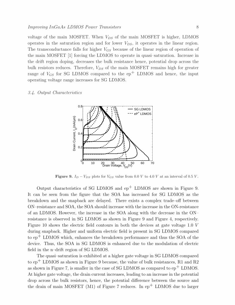
Figure 9. ID − VDS plots for VGS value from 0.0 V to 4.0 V at an interval of 0.5 V .
Output characteristics of SG LDMOS and ep+ LDMOS are shown in Figure 9.
It can be seen from the figure that the SOA has increased for SG LDMOS as the
breakdown and the snapback are delayed. There exists a complex trade–off between
ON–resistance and SOA, the SOA should increase with the increase in the ON-resistance
of an LDMOS. However, the increase in the SOA along with the decrease in the ON–
resistance is observed in SG LDMOS as shown in Figure 9 and Figure 4, respectively.
Figure 10 shows the electric field contours in both the devices at gate voltage 1.0 V
during snapback. Higher and uniform electric field is present in SG LDMOS compared
to ep+ LDMOS which, enhances the breakdown performance and thus the SOA of the
device. Thus, the SOA in SG LDMOS is enhanced due to the modulation of electric
field in the n–drift region of SG LDMOS.
The quasi–saturation is exhibited at a higher gate voltage in SG LDMOS compared
to ep+ LDMOS as shown in Figure 9 because, the value of bulk resistances, R1 and R2
as shown in Figure 7, is smaller in the case of SG LDMOS as compared to ep+ LDMOS.
At higher gate voltage, the drain current increases, leading to an increase in the potential
drop across the bulk resistors, hence, the potential difference between the source and
the drain of main MOSFET (M1) of Figure 7 reduces. In ep+ LDMOS due to larger

Improving InGaAs LDMOS Power Transistors 9
0 1 2 3 4 5 6
0
1
Microns
Mic
ron
s
0
2.82e+05
5.65e+05
8.48e+05
1.13e+06
(a)
0 1 2 3 4 5 6
0
1
Microns
Mic
ron
s
0
2.82e+05
5.65e+05
8.48e+05
1.13e+06
(b)
Figure 10. Electric field (V/cm) distribution in (a) ep+ LDMOS and (b) SG LDMOS
at VGS = 1.0 V during snapback.
drop across the bulk resistors, M1 reaches linear region and hence, ep+ LDMOS goes
into quasi–saturation. SG LDMOS stays in saturation region for a longer range of gate
voltage due to the lesser value of the bulk resistance hence, the quasi–saturation occurs
at a larger gate voltage as for SG LDMOS as compared to ep+ LDMOS shown in
Figure 9.
Improving InGaAs LDMOS Power Transistors 10
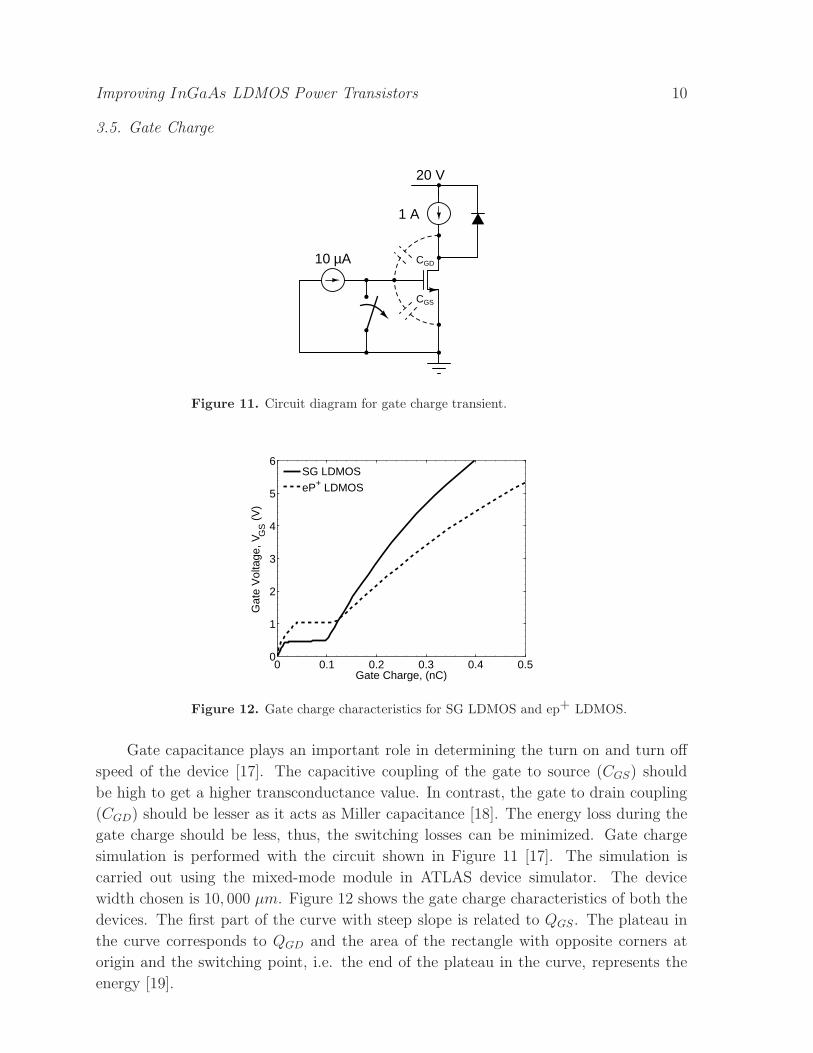
3.5. Gate Charge
20 V
1 A
10 µA
CGS
CGD
Figure 11. Circuit diagram for gate charge transient.
0 0.1 0.2 0.3 0.4 0.50
1
2
3
4
5
6
Gate Charge, (nC)
Gat
e V
olta
ge, V
GS (
V)
SG LDMOS
eP+ LDMOS
Figure 12. Gate charge characteristics for SG LDMOS and ep+ LDMOS.
Gate capacitance plays an important role in determining the turn on and turn off
speed of the device [17]. The capacitive coupling of the gate to source (CGS) should
be high to get a higher transconductance value. In contrast, the gate to drain coupling
(CGD) should be lesser as it acts as Miller capacitance [18]. The energy loss during the
gate charge should be less, thus, the switching losses can be minimized. Gate charge
simulation is performed with the circuit shown in Figure 11 [17]. The simulation is
carried out using the mixed-mode module in ATLAS device simulator. The device
width chosen is 10, 000 µm. Figure 12 shows the gate charge characteristics of both the
devices. The first part of the curve with steep slope is related to QGS. The plateau in
the curve corresponds to QGD and the area of the rectangle with opposite corners at
origin and the switching point, i.e. the end of the plateau in the curve, represents the
energy [19].
Improving InGaAs LDMOS Power Transistors 11
The initial rise of the curve shows a lesser slope for SG LDMOS as compared
to ep+ LDMOS. Hence, SG LDMOS has a higher input capacitance than that
of ep+ LDMOS. CGD for SG LDMOS and ep+ LDMOS is 20.1 nF/mm2 and
29.0 nF/mm2, respectively. There is 30.8 % reduction in gate to drain capacitance
for SG LDMOS in comparison with ep+ LDMOS. This is ascribed to the stepped gate
architecture which, increase the dielectric thickness between the gate and the drain in
SG LDMOS. Thus, reducing the detrimental effect of Miller capacitance on the amplifier
circuits. The total energy required to for switching in SG LDMOS and ep+ LDMOS
is 47.8 pJ and 121.8 pJ , respectively. The SG LDMOS exhibits a 60.7 % decrease in
the switching loss as compared to the ep+ LDMOS. The gate charge (QG) at a gate
voltage of 5 V is 5.28 nC/mm2 and 7.95 nC/mm2 for SG LDMOS and ep+ LDMOS,
respectively. Thus, the SG LDMOS exhibits a 33.6 % improvement in the gate charge
characteristics as compared to the ep+ LDMOS. The ON-resistance was reduced for
SG LDMOS as compared to ep+ LDMOS as shown in Section 3.2. Thus, the value of
RON × QG has also reduced by 62.6 % in SG LDMOS compared to ep+ LDMOS.
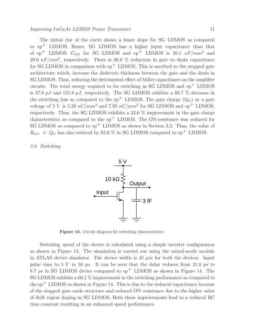
3.6. Switching
3 fF
Output
Input
5 V
10 kΩ
Figure 13. Circuit diagram for switching characteristics.
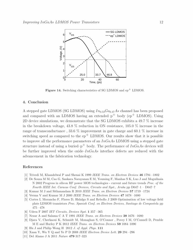
Switching speed of the device is calculated using a simple inverter configuration
as shown in Figure 13. The simulation is carried out using the mixed-mode module
in ATLAS device simulator. The device width is 45 µm for both the devices. Input
pulse rises to 5 V in 50 ps. It can be seen that the delay reduces from 21.8 ps to
8.7 ps in SG LDMOS device compared to ep+ LDMOS as shown in Figure 14. The
SG LDMOS exhibits a 60.1 % improvement in the switching performance as compared to
the ep+ LDMOS as shown in Figure 14. This is due to the reduced capacitance because
of the stepped gate oxide structure and reduced ON–resistance due to the higher value
of drift region doping in SG LDMOS. Both these improvements lead to a reduced RC
time constant resulting in an enhanced speed performance.
Improving InGaAs LDMOS Power Transistors 12
0 20 40 600
1
2
3
4
5
6
Time, (ps)
Vol
tage
, (V
)
25.0 33.7 46.8
VDS
VGS
SG LDMOS
ep+ LDMOS
Figure 14. Switching characteristics of SG LDMOS and ep+ LDMOS.
4. Conclusion
A stepped gate LDMOS (SG LDMOS) using In0.53Ga0.47As channel has been proposed
and compared with an LDMOS having an extended–p+ body (ep+ LDMOS). Using
2D device simulations, we demonstrate that the SG LDMOS exhibits a 49.7 % increase
in the breakdown voltage, 43.8 % reduction in ON–resistance, 105.0 % increase in the
range of transconductance , 33.6 % improvement in gate charge and 60.1 % increase in
switching speed as compared to the ep+ LDMOS. Our results show that it is possible
to improve all the performance parameters of an InGaAs LDMOS using a stepped gate
structure instead of using a buried–p+ body. The performance of InGaAs devices will
be further improved when the oxide–InGaAs interface defects are reduced with the
advancement in the fabrication technology.
References
[1] Trivedi M, Khandelwal P and Shenai K 1999 IEEE Trans. on Electron Devices 46 1794 –1802
[2] De Souza M M, Cao G, Sankara Narayanan E M, Youming F, Manhas S K, Luo J and Moguilnaia
N 2002 Progress in silicon RF power MOS technologies - current and future trends Proc. of the
Fourth IEEE Int. Caracas Conf. Devices, Circuits and Syst., Aruba pp D047–1 – D047–7
[3] Kumar M J and Sithanandam R 2010 IEEE Trans. on Electron Devices 57 1719 –1724
[4] Verma V and Kumar M J 2000 IEEE Trans. on Electron Devices 47 1678 –1680
[5] Cortes I, Morancho F, Flores D, Hidalgo S and Rebollo J 2009 Optimisation of low voltage field
plate LDMOS transistors Proc. Spanish Conf. on Electron Devices, Santiago de Compostela pp
475 –478
[6] Udrea F 2007 IET Circuits, Devices Syst. 1 357 –365
[7] Nezar A and Salama C A T 1991 IEEE Trans. on Electron Devices 38 1676 –1680
[8] Djara V, Cherkaoui K, Schmidt M, Monaghan S, O’Connor , Povey I M, O’Connell D, Pemble
M E and Hurley P K 2012 IEEE Trans. on Electron Devices 59 1084–1090
[9] Hu J and Philip Wong H 2012 J. of Appl. Phys. 111
[10] Xuan Y, Wu Y Q and Ye P D 2008 IEEE Electron Device Lett. 29 294 –296
[11] Del Alamo J A 2011 Nature 479 317–323
Improving InGaAs LDMOS Power Transistors 13
[12] Radosavljevic M, Chu-Kung B, Corcoran S, Dewey G, Hudait M K, Fastenau J M, Kavalieros J,
Liu W K, Lubyshev D, Metz M, Millard K, Mukherjee N, Rachmady W, Shah U and Chau R
2009 Advanced high-k gate dielectric for high-performance short-channel In0.7Ga0.3As quantum
well field effect transistors on silicon substrate for low power logic applications IEDM Tech. Dig.,
2009 pp 1 –4
[13] Steighner J B, Yuan J S and Liu Y 2011 IEEE Trans. on Electron Devices 58 180 –189
[14] Silvaco Inc. Santa Clara, CA 2011 Atlas User’s Manual: Device Simulation Software
[15] Johnson G A, Kapoor V J, Shokrani M, Messick L J, Nguyen R, Stall R A and McKee M A 1991
IEEE Trans. on Microwave Theory and Tech. 39 1069 –1075
[16] Sun S C and Plummer J D 1980 IEEE Trans. on Electron Devices 27 356 – 367
[17] Saxena R S and Kumar M J 2009 IEEE Trans. on Electron Devices 56 1355 –1359
[18] Hueting R J E, Hijzen E A, Heringa A, Ludikhuize A W and M A A in’t Zandt 2004 IEEE Trans.
on Electron Devices 51 1323 – 1330
[19] International Rectifier El Segundo, CA Use gate charge to design the gate drive circuit for power
MOSFETs and IGBT application Note AN-944