Improvements in MEMS gyroscope production as a result of using in situ, aligned, current-limited...
5
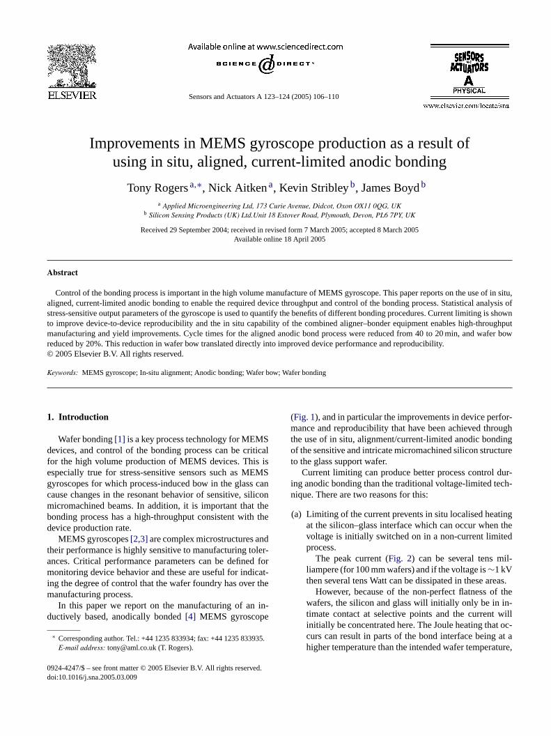
Sensors and Actuators A 123–124 (2005) 106–110 Improvements in MEMS gyroscope production as a result of using in situ, aligned, current-limited anodic bonding Tony Rogers a,∗ , Nick Aitken a , Kevin Stribley b , James Boyd b a Applied Microengineering Ltd, 173 Curie Avenue, Didcot, Oxon OX11 0QG, UK b Silicon Sensing Products (UK) Ltd.Unit 18 Estover Road, Plymouth, Devon, PL6 7PY, UK Received 29 September 2004; received in revised form 7 March 2005; accepted 8 March 2005 Available online 18 April 2005 Abstract Control of the bonding process is important in the high volume manufacture of MEMS gyroscope. This paper reports on the use of in situ, aligned, current-limited anodic bonding to enable the required device throughput and control of the bonding process. Statistical analysis of stress-sensitive output parameters of the gyroscope is used to quantify the benefits of different bonding procedures. Current limiting is shown to improve device-to-device reproducibility and the in situ capability of the combined aligner–bonder equipment enables high-throughput manufacturing and yield improvements. Cycle times for the aligned anodic bond process were reduced from 40 to 20 min, and wafer bow reduced by 20%. This reduction in wafer bow translated directly into improved device performance and reproducibility. © 2005 Elsevier B.V. All rights reserved. Keywords: MEMS gyroscope; In-situ alignment; Anodic bonding; Wafer bow; Wafer bonding 1. Introduction Wafer bonding [1] is a key process technology for MEMS devices, and control of the bonding process can be critical for the high volume production of MEMS devices. This is especially true for stress-sensitive sensors such as MEMS gyroscopes for which process-induced bow in the glass can cause changes in the resonant behavior of sensitive, silicon micromachined beams. In addition, it is important that the bonding process has a high-throughput consistent with the device production rate. MEMS gyroscopes [2,3] are complex microstructures and their performance is highly sensitive to manufacturing toler- ances. Critical performance parameters can be defined for monitoring device behavior and these are useful for indicat- ing the degree of control that the wafer foundry has over the manufacturing process. In this paper we report on the manufacturing of an in- ductively based, anodically bonded [4] MEMS gyroscope ∗ Corresponding author. Tel.: +44 1235 833934; fax: +44 1235 833935. E-mail address: [email protected] (T. Rogers). (Fig. 1), and in particular the improvements in device perfor- mance and reproducibility that have been achieved through the use of in situ, alignment/current-limited anodic bonding of the sensitive and intricate micromachined silicon structure to the glass support wafer. Current limiting can produce better process control dur- ing anodic bonding than the traditional voltage-limited tech- nique. There are two reasons for this: (a) Limiting of the current prevents in situ localised heating at the silicon–glass interface which can occur when the voltage is initially switched on in a non-current limited process. The peak current (Fig. 2) can be several tens mil- liampere (for 100 mm wafers) and if the voltage is ∼1 kV then several tens Watt can be dissipated in these areas. However, because of the non-perfect flatness of the wafers, the silicon and glass will initially only be in in- timate contact at selective points and the current will initially be concentrated here. The Joule heating that oc- curs can result in parts of the bond interface being at a higher temperature than the intended wafer temperature, 0924-4247/$ – see front matter © 2005 Elsevier B.V. All rights reserved. doi:10.1016/j.sna.2005.03.009
-
Upload
tony-rogers -
Category
Documents
-
view
221 -
download
2
Transcript of Improvements in MEMS gyroscope production as a result of using in situ, aligned, current-limited...
Sensors and Actuators A 123–124 (2005) 106–110
Improvements in MEMS gyroscope production as a result ofusing in situ, aligned, current-limited anodic bonding
Tony Rogersa,∗, Nick Aitkena, Kevin Stribleyb, James Boydb
a Applied Microengineering Ltd, 173 Curie Avenue, Didcot, Oxon OX11 0QG, UKb Silicon Sensing Products (UK) Ltd.Unit 18 Estover Road, Plymouth, Devon, PL6 7PY, UK
Received 29 September 2004; received in revised form 7 March 2005; accepted 8 March 2005Available online 18 April 2005
Abstract
Control of the bonding process is important in the high volume manufacture of MEMS gyroscope. This paper reports on the use of in situ,aligned, current-limited anodic bonding to enable the required device throughput and control of the bonding process. Statistical analysis ofstress-sensitive output parameters of the gyroscope is used to quantify the benefits of different bonding procedures. Current limiting is shownto improve device-to-device reproducibility and the in situ capability of the combined aligner–bonder equipment enables high-throughputm wafer bowr©
K
1
dfegcmbd
tamim
d
for-oughingture
dur-ch-
tingthe
ed
il-
eas.f then-willt oc-at ature,
0d
anufacturing and yield improvements. Cycle times for the aligned anodic bond process were reduced from 40 to 20 min, andeduced by 20%. This reduction in wafer bow translated directly into improved device performance and reproducibility.
2005 Elsevier B.V. All rights reserved.
eywords: MEMS gyroscope; In-situ alignment; Anodic bonding; Wafer bow; Wafer bonding
. Introduction
Wafer bonding[1] is a key process technology for MEMSevices, and control of the bonding process can be critical
or the high volume production of MEMS devices. This isspecially true for stress-sensitive sensors such as MEMSyroscopes for which process-induced bow in the glass canause changes in the resonant behavior of sensitive, siliconicromachined beams. In addition, it is important that theonding process has a high-throughput consistent with theevice production rate.
MEMS gyroscopes[2,3] are complex microstructures andheir performance is highly sensitive to manufacturing toler-nces. Critical performance parameters can be defined foronitoring device behavior and these are useful for indicat-
ng the degree of control that the wafer foundry has over theanufacturing process.In this paper we report on the manufacturing of an in-
uctively based, anodically bonded[4] MEMS gyroscope
∗ Corresponding author. Tel.: +44 1235 833934; fax: +44 1235 833935.E-mail address: [email protected] (T. Rogers).
(Fig. 1), and in particular the improvements in device permance and reproducibility that have been achieved thrthe use of in situ, alignment/current-limited anodic bondof the sensitive and intricate micromachined silicon structo the glass support wafer.
Current limiting can produce better process controling anodic bonding than the traditional voltage-limited tenique. There are two reasons for this:
(a) Limiting of the current prevents in situ localised heaat the silicon–glass interface which can occur whenvoltage is initially switched on in a non-current limitprocess.
The peak current (Fig. 2) can be several tens mliampere (for 100 mm wafers) and if the voltage is∼1 kVthen several tens Watt can be dissipated in these ar
However, because of the non-perfect flatness owafers, the silicon and glass will initially only be in itimate contact at selective points and the currentinitially be concentrated here. The Joule heating thacurs can result in parts of the bond interface beinghigher temperature than the intended wafer tempera
924-4247/$ – see front matter © 2005 Elsevier B.V. All rights reserved.oi:10.1016/j.sna.2005.03.009
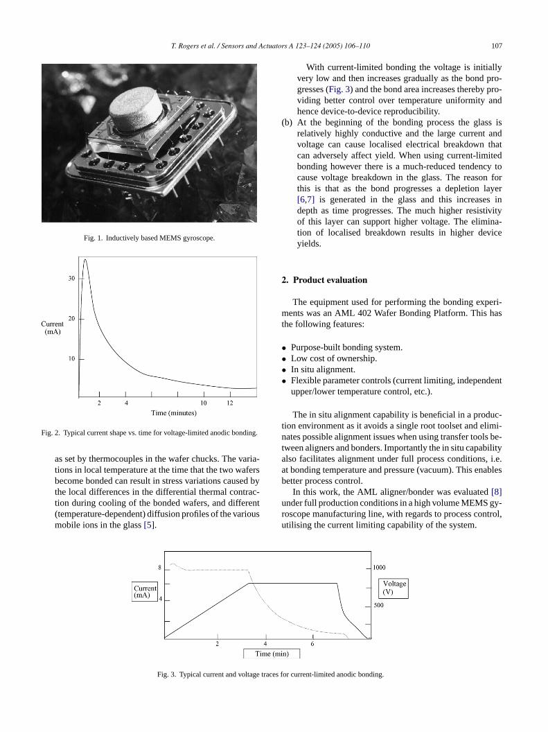
T. Rogers et al. / Sensors and Actuators A 123–124 (2005) 106–110 107
Fig. 1. Inductively based MEMS gyroscope.
Fig. 2. Typical current shape vs. time for voltage-limited anodic bonding.
as set by thermocouples in the wafer chucks. The varia-tions in local temperature at the time that the two wafersbecome bonded can result in stress variations caused bythe local differences in the differential thermal contrac-tion during cooling of the bonded wafers, and different(temperature-dependent) diffusion profiles of the variousmobile ions in the glass[5].
With current-limited bonding the voltage is initiallyvery low and then increases gradually as the bond pro-gresses (Fig. 3) and the bond area increases thereby pro-viding better control over temperature uniformity andhence device-to-device reproducibility.
(b) At the beginning of the bonding process the glass isrelatively highly conductive and the large current andvoltage can cause localised electrical breakdown thatcan adversely affect yield. When using current-limitedbonding however there is a much-reduced tendency tocause voltage breakdown in the glass. The reason forthis is that as the bond progresses a depletion layer[6,7] is generated in the glass and this increases indepth as time progresses. The much higher resistivityof this layer can support higher voltage. The elimina-tion of localised breakdown results in higher deviceyields.
2. Product evaluation
The equipment used for performing the bonding experi-ments was an AML 402 Wafer Bonding Platform. This hasthe following features:
•••• ent
uc-t limi-n ls be-t bilitya , i.e.a ablesb
u y-r trol,u
Fig. 3. Typical current and voltage trace
Purpose-built bonding system.Low cost of ownership.In situ alignment.Flexible parameter controls (current limiting, independupper/lower temperature control, etc.).
The in situ alignment capability is beneficial in a prodion environment as it avoids a single root toolset and eates possible alignment issues when using transfer too
ween aligners and bonders. Importantly the in situ capalso facilitates alignment under full process conditionst bonding temperature and pressure (vacuum). This enetter process control.
In this work, the AML aligner/bonder was evaluated[8]nder full production conditions in a high volume MEMS goscope manufacturing line, with regards to process contilising the current limiting capability of the system.
s for current-limited anodic bonding.
108 T. Rogers et al. / Sensors and Actuators A 123–124 (2005) 106–110
The production targets were as follows (to match processtransfer specifications):
– Bond time = <40 min– Wafer bow = <70�m– Alignment = <10�m
The procedure used to determine the impact of this noveltype of in situ, aligned bonding was to fabricate a batchof wafers and to further process these bonded wafers toproduce fully packaged gyroscopes. These devices werethen analysed by measuring key output parameters that arehighly sensitive to packaging stress. Because the anodicbond between the glass and the silicon is used to anchor thesensitive microstructure used to measure the Coriolis force,variations in bond characteristics are expected to show up asstress-induced variation in the stability of this measurement.Comparisons were then made between the devices madeusing voltage- and current-limited bonding. Further com-parisons were then done using the AML 402 as-installed,and then an upgraded machine which specifically addressesfast bond cycling to satisfy the high-throughput, gyroscopemanufacturing requirements, yet still maintains the closecontrol of the bonding process to produce device stabilityand reproducibility.
A bonding temperature of 370◦C was selected as this pro-v esst le toa dard,v
3
( tureo andt entm
thec gs
sig-n ondt -q clet
••
tw ec-t
••
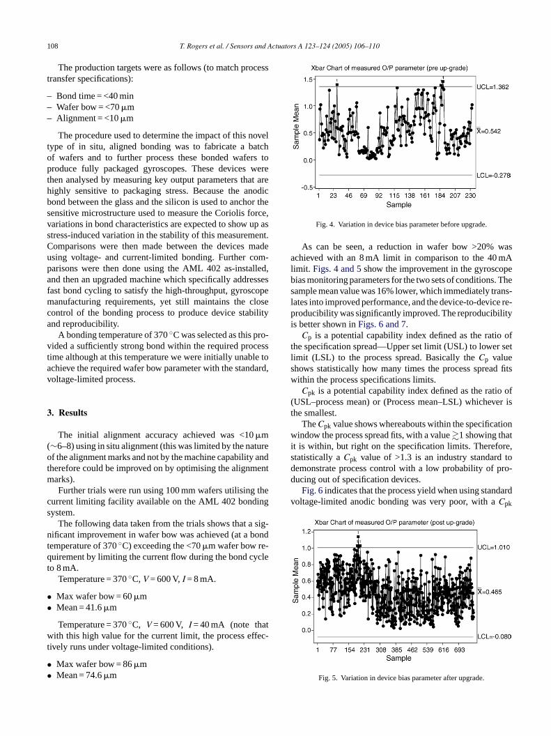
Fig. 4. Variation in device bias parameter before upgrade.
As can be seen, a reduction in wafer bow >20% wasachieved with an 8 mA limit in comparison to the 40 mAlimit. Figs. 4 and 5show the improvement in the gyroscopebias monitoring parameters for the two sets of conditions. Thesample mean value was 16% lower, which immediately trans-lates into improved performance, and the device-to-device re-producibility was significantly improved. The reproducibilityis better shown inFigs. 6 and 7.
Cp is a potential capability index defined as the ratio ofthe specification spread—Upper set limit (USL) to lower setlimit (LSL) to the process spread. Basically theCp valueshows statistically how many times the process spread fitswithin the process specifications limits.
Cpk is a potential capability index defined as the ratio of(USL–process mean) or (Process mean–LSL) whichever isthe smallest.
TheCpk value shows whereabouts within the specificationwindow the process spread fits, with a value�1 showing thatit is within, but right on the specification limits. Therefore,statistically aCpk value of >1.3 is an industry standard todemonstrate process control with a low probability of pro-ducing out of specification devices.
Fig. 6indicates that the process yield when using standardvoltage-limited anodic bonding was very poor, with aCpk
ided a sufficiently strong bond within the required procime although at this temperature we were initially unabchieve the required wafer bow parameter with the stanoltage-limited process.
. Results
The initial alignment accuracy achieved was <10�m∼6–8) using in situ alignment (this was limited by the naf the alignment marks and not by the machine capability
herefore could be improved on by optimising the alignmarks).Further trials were run using 100 mm wafers utilising
urrent limiting facility available on the AML 402 bondinystem.
The following data taken from the trials shows that aificant improvement in wafer bow was achieved (at a b
emperature of 370◦C) exceeding the <70�m wafer bow reuirement by limiting the current flow during the bond cy
o 8 mA.Temperature = 370◦C, V = 600 V,I = 8 mA.
Max wafer bow = 60�mMean = 41.6�m
Temperature = 370◦C, V = 600 V, I = 40 mA (note thaith this high value for the current limit, the process eff
ively runs under voltage-limited conditions).
Max wafer bow = 86�mMean = 74.6�m
Fig. 5. Variation in device bias parameter after upgrade.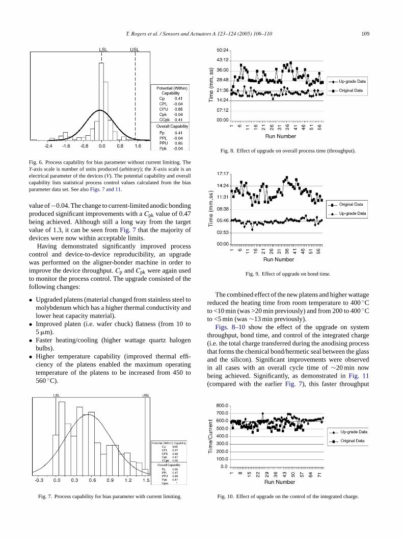
T. Rogers et al. / Sensors and Actuators A 123–124 (2005) 106–110 109
Fig. 6. Process capability for bias parameter without current limiting. TheY-axis scale is number of units produced (arbitrary); theX-axis scale is anelectrical parameter of the devices (V). The potential capability and overallcapability lists statistical process control values calculated from the biasparameter data set. See alsoFigs. 7 and 11.
value of−0.04. The change to current-limited anodic bondingproduced significant improvements with aCpk value of 0.47being achieved. Although still a long way from the targetvalue of 1.3, it can be seen fromFig. 7 that the majority ofdevices were now within acceptable limits.
Having demonstrated significantly improved processcontrol and device-to-device reproducibility, an upgradewas performed on the aligner-bonder machine in order toimprove the device throughput.Cp andCpk were again usedto monitor the process control. The upgrade consisted of thefollowing changes:
• Upgraded platens (material changed from stainless steel tomolybdenum which has a higher thermal conductivity andlower heat capacity material).
• Improved platen (i.e. wafer chuck) flatness (from 10 to5�m).
• Faster heating/cooling (higher wattage quartz halogenbulbs).
• Higher temperature capability (improved thermal effi-ciency of the platens enabled the maximum operatingtemperature of the platens to be increased from 450 to560◦C).
Fig. 8. Effect of upgrade on overall process time (throughput).
Fig. 9. Effect of upgrade on bond time.
The combined effect of the new platens and higher wattagereduced the heating time from room temperature to 400◦Cto <10 min (was >20 min previously) and from 200 to 400◦Cto <5 min (was∼13 min previously).
Figs. 8–10show the effect of the upgrade on systemthroughput, bond time, and control of the integrated charge(i.e. the total charge transferred during the anodising processthat forms the chemical bond/hermetic seal between the glassand the silicon). Significant improvements were observedin all cases with an overall cycle time of∼20 min nowbeing achieved. Significantly, as demonstrated inFig. 11(compared with the earlierFig. 7), this faster throughput
Fig. 10. Effect of upgrade on the control of the integrated charge.
Fig. 7. Process capability for bias parameter with current limiting.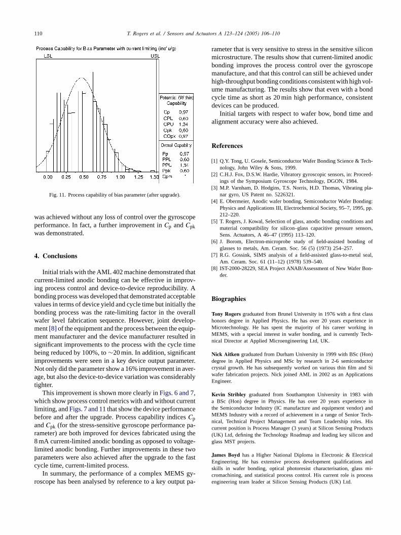
110 T. Rogers et al. / Sensors and Actuators A 123–124 (2005) 106–110
Fig. 11. Process capability of bias parameter (after upgrade).
was achieved without any loss of control over the gyroscopeperformance. In fact, a further improvement inCp andCpkwas demonstrated.
4. Conclusions
Initial trials with the AML 402 machine demonstrated thatcurrent-limited anodic bonding can be effective in improv-ing process control and device-to-device reproducibility. Abonding process was developed that demonstrated acceptablvalues in terms of device yield and cycle time but initially thebonding process was the rate-limiting factor in the overallwafer level fabrication sequence. However, joint develop-ment[8] of the equipment and the process between the equip-ment manufacturer and the device manufacturer resulted insignificant improvements to the process with the cycle timebeing reduced by 100%, to∼20 min. In addition, significantimprovements were seen in a key device output parameter.Not only did the parameter show a 16% improvement in aver-age, but also the device-to-device variation was considerablytighter.
This improvement is shown more clearly inFigs. 6 and 7,which show process control metrics with and without currentlimiting, andFigs. 7 and 11that show the device performancebefore and after the upgrade. Process capability indicesCpa pa-r the8 age-l twop e fasc
gy-r ut pa
rameter that is very sensitive to stress in the sensitive siliconmicrostructure. The results show that current-limited anodicbonding improves the process control over the gyroscopemanufacture, and that this control can still be achieved underhigh-throughput bonding conditions consistent with high vol-ume manufacturing. The results show that even with a bondcycle time as short as 20 min high performance, consistentdevices can be produced.
Initial targets with respect to wafer bow, bond time andalignment accuracy were also achieved.
References
[1] Q.Y. Tong, U. Gosele, Semiconductor Wafer Bonding Science & Tech-nology, John Wiley & Sons, 1999.
[2] C.H.J. Fox, D.S.W. Hardie, Vibratory gyroscopic sensors, in: Proceed-ings of the Symposium Gyroscope Technology, DGON, 1984.
[3] M.P. Varnham, D. Hodgins, T.S. Norris, H.D. Thomas, Vibrating pla-nar gyro, US Patent no. 5226321.
[4] E. Obermeier, Anodic wafer bonding, Semiconductor Wafer Bonding:Physics and Applications III, Electrochemical Society, 95–7, 1995, pp.212–220.
[5] T. Rogers, J. Kowal, Selection of glass, anodic bonding conditions andmaterial compatibility for silicon–glass capacitive pressure sensors,Sens. Actuators, A 46–47 (1995) 113–120.
[6] J. Borom, Electron-microprobe study of field-assisted bonding ofglasses to metals, Am. Ceram. Soc. 56 (5) (1973) 254–257.
[ seal,
[ on-
B
T assh nce inM g inM ech-n
N on)d uctorc d Siw onsE
K itha ce int r) andM ech-n . Hisc oducts( andg
J calE s ands mi-c ocesse
ndCpk (for the stress-sensitive gyroscope performanceameter) are both improved for devices fabricated usingmA current-limited anodic bonding as opposed to volt
imited anodic bonding. Further improvements in thesearameters were also achieved after the upgrade to thycle time, current-limited process.
In summary, the performance of a complex MEMSoscope has been analysed by reference to a key outp
e
t
-
7] R.G. Gossink, SIMS analysis of a field-assisted glass-to-metalAm. Ceram. Soc. 61 (11–12) (1978) 539–540.
8] IST-2000-28229, SEA Project ANAB/Assessment of New Wafer Bder.
iographies
ony Rogers graduated from Brunel University in 1976 with a first clonors degree in Applied Physics. He has over 20 years experieicrotechnology. He has spent the majority of his career workinEMS, with a special interest in wafer bonding, and is currently Tical Director at Applied Microengineering Ltd, UK.
ick Aitken graduated from Durham University in 1999 with BSc (Hegree in Applied Physics and MSc by research in 2-6 semicondrystal growth. He has subsequently worked on various thin film anafer fabrication projects. Nick joined AML in 2002 as an Applicatingineer.
evin Stribley graduated from Southampton University in 1983 wBSc (Hon) degree in Physics. He has over 20 years experien
he Semiconductor Industry (IC manufacture and equipment vendoEMS Industry with a record of achievement in a range of Senior Tical, Technical Project Management and Team Leadership rolesurrent position is Process Manager (3 years) at Silicon Sensing PrUK) Ltd, defining the Technology Roadmap and leading key siliconlass MST projects.
ames Boyd has a Higher National Diploma in Electronic & Electringineering. He has extensive process development qualificationkills in wafer bonding, optical photoresist characterisation, glassromachining, and statistical process control. His current role is prngineering team leader at Silicon Sensing Products (UK) Ltd.