
Improved N-Type 4h-Sic Epitaxial Layer Radiation Detectors ...
116
University of South Carolina University of South Carolina Scholar Commons Scholar Commons Theses and Dissertations 2017 Improved N-Type 4h-Sic Epitaxial Layer Radiation Detectors and Improved N-Type 4h-Sic Epitaxial Layer Radiation Detectors and Noise Analysis of Front-End Readout Electronics Noise Analysis of Front-End Readout Electronics Khai V. Nguyen University of South Carolina Follow this and additional works at: https://scholarcommons.sc.edu/etd Part of the Electrical and Electronics Commons Recommended Citation Recommended Citation V. Nguyen, K.(2017). Improved N-Type 4h-Sic Epitaxial Layer Radiation Detectors and Noise Analysis of Front-End Readout Electronics. (Doctoral dissertation). Retrieved from https://scholarcommons.sc.edu/ etd/4430 This Open Access Dissertation is brought to you by Scholar Commons. It has been accepted for inclusion in Theses and Dissertations by an authorized administrator of Scholar Commons. For more information, please contact [email protected].
Transcript of Improved N-Type 4h-Sic Epitaxial Layer Radiation Detectors ...

University of South Carolina University of South Carolina
Scholar Commons Scholar Commons
Theses and Dissertations
2017
Improved N-Type 4h-Sic Epitaxial Layer Radiation Detectors and Improved N-Type 4h-Sic Epitaxial Layer Radiation Detectors and
Noise Analysis of Front-End Readout Electronics Noise Analysis of Front-End Readout Electronics
Khai V Nguyen University of South Carolina
Follow this and additional works at httpsscholarcommonssceduetd
Part of the Electrical and Electronics Commons
Recommended Citation Recommended Citation V Nguyen K(2017) Improved N-Type 4h-Sic Epitaxial Layer Radiation Detectors and Noise Analysis of Front-End Readout Electronics (Doctoral dissertation) Retrieved from httpsscholarcommonssceduetd4430
This Open Access Dissertation is brought to you by Scholar Commons It has been accepted for inclusion in Theses and Dissertations by an authorized administrator of Scholar Commons For more information please contact digresmailboxscedu
IMPROVED N-TYPE 4H-SIC EPITAXIAL LAYER RADIATION DETECTORS AND
NOISE ANALYSIS OF FRONT-END READOUT ELECTRONICS
by
Khai V Nguyen
Bachelor of Science
University of South Carolina 2013
Master of Engineering
University of South Carolina 2015
Submitted in Partial Fulfillment of the Requirements
For the Degree of Doctor of Philosophy in
Electrical Engineering
College of Engineering and Computing
University of South Carolina
2017
Accepted by
Krishna C Mandal Major Professor
Enrico Santi Committee Member
Guoan Wang Committee Member
Yuriy V Pershin Committee Member
Cheryl L Addy Vice Provost and Dean of the Graduate School
ii
copy Copyright by Khai V Nguyen 2017
All Rights Reserved
iii
DEDICATION
I would like to dedicate this work to my dear wife Lam who has been a constant
source of support and encouragement in this endeavor I am very thankful to have you by
my side Without you I would never have made it thus far
iv
ACKNOWLEDGEMENTS
First and foremost I am sincerely grateful to my graduate advisor Dr Krishna C
Mandal for welcoming me into his research group His tremendous enthusiasm guidance
and support have enabled me to make great strides forward in my career and in my
understanding of semiconductors He has continued to inspire my passion for science
from my first day in his class as an undergraduate electrical engineering student through
to this day I would also like to thank my committee members Dr Enrico Santi Dr
Guoan Wang and Dr Yuriy V Pershin for sacrificing a portion of their time to provide
guidance and support of my work
I would like to thank the Chairman of the Department of Electrical Engineering
Professor Roger Dougal for his guidance and words of wisdom that set me on the path to
success in both life and as an engineer
For their contributions in the research performed in this work I would like to
thank the following people
Dr Sandeep K Chaudhuri for his extraordinary effort and tireless
patience invested in setting up the DLTS and passing on his knowledge of
radiation measurements and instrument calibration to me
Dr Shuguo Ma (College of Engineering and Computing University of
South Carolina) for performing XPS characterization
v
The staff of the Institute for Electronics and Nanotechnology (IEN) at
Georgia Tech for organizing the equipment training schedule such that
two visits were enough to be qualified and added as a user for all of the
tools necessary for fabricating the edge-terminated detectors
Nat Patterson David London Ashley Burt Alicia Williams David Metts
Jenny Balestrero Lauren Ridings and all those I have forgotten who have
provided both their expertise and kind words throughout my time here at
USC
Finally I would like to thank my fellow lab members Dr Sandeep K Chaudhuri
Dr Sandip Das Dr Mohammad A Mannan Kelvin Zavalla Cihan Oner and Towhid A
Chowdhuri for their scientific inquisitiveness humor friendship and support
vi
ABSTRACT
Schottky barrier radiation detectors were fabricated on n-type 4H-SiC
epitaxial layers (12 ndash 50 microm) grown by hot wall CVD process on highly nitrogen doped
4H-SiC (0001) substrates with 4-8ordm off-cut towards the direction Ni4H-SiC
Schottky barrier radiation detectors a very low leakage current of 018 nA at 250 V bias
revealing low thermal noise was observed in current-voltage (I-V) measurements Using
a thermionic emission model junction properties such as barrier height of ge110 eV and
an ideality factor of le129 were determined An effective carrier concentration of
103times1015
cm-3
was calculated by capacitance-voltage (C-V) measurement Deep level
transient spectroscopy (DLTS) was used to investigate electrically active defects in
epilayer Defect parameters such as activation energy capture cross-section and density
of defects were calculated from Arrhenius plots DLTS revealed the presence of shallow
level defects related to titanium impurities electrically active lifetime killer Z12 defect
and deep level defects assigned as EH67 which are related to carbon and carbon-silicon
vacancies The density of Z12 defect the most detrimental to detector performance was
16times1012
cm-3
orders of magnitude lower compared to other 4H-SiC detectors
Detector performances were evaluated in terms of the energy resolution at full-
width at half-maximum (FWHM) using pulse height spectroscopy (PHS) measurements
with 01 microCi 241
Am source Charge collection efficiency was investigated using a drift-
diffusion charge transport model The energy resolution for 5486 MeV alpha particles
vii
was 166 keV with charge collection efficiency of 226 Electronic noise analysis of
front-end readout system was carried out in terms of equivalent noise charge (ENC) in
order to study the contribution of white series noise pink noise ( parallel and frasl
series) and white parallel noise to the total electronic noise in the detection system
New edge termination was developed using surface passivating layers of silicon
dioxide (SiO2) and silicon nitride (Si3N4) in order to improve detector performance With
edge termination reverse leakage current of Ni4H-SiC epilayer detector was improved
significantly (nA to pA) leading to an increased signal-to-noise ratio Improved Schottky
properties such as barrier height of ~17 eV and diode ideality factor of ~107 were
observed indicating a better surface uniformity that enhanced charge collection
efficiency C-V measurement confirmed a doping concentration of 24 x 1014
cm-3
ensuring a fully depleted (~20 microm) detector at bias voltages as low as ~70 V DLTS
analysis showed a decreased concentration of performance limiting Z12 defect level and
absence of EH67 deep-levels with edge termination ensuing a more complete charge
collection Alpha spectroscopy measurements revealed an improved detector energy
resolution from ~07 to ~04 for 548 MeV alpha particles with edge termination
4H-SiC epitaxial detector with ruthenium (Ru) Schottky barrier contact (in
addition to Ni being used in above studies) was investigated for operation in harsh
environments with high temperature and high radiation Ru4H-SiC Schottky detectors
exhibited excellent rectification and improved junction properties even without edge
termination However inhomogeneity of the Schottky barrier heights was observed due
to interfacial defects resulting from a solid-state reaction involving Ru Si and C As a
result pulse-height spectra with 241
Am source were broad and the three characteristic
viii
alpha peaks were not resolved The energy resolution was calculated to be ~ 075 at
180 V reverse bias at room temperature
ix
TABLE OF CONTENTS
Dedication iii
Acknowledgements iv
Abstract vi
Table of Contents ix
List of Tables xii
List of Figures xiii
List of Abbreviations xvii
CHAPTER 1 General Introduction 1
Dissertation Introduction 1 11
Dissertation Overview 4 12
structure and properties of 4h-sic 7 13
Growth of 4H-Silicon Carbide Material 8 14
CHAPTER 2 Detector Fabrication and Characterization 11
Overview 11 21
Epitaxial 4H-Silicon Carbide Detector Material 12 22
Ni4H-SiC Schottky Barrier Detector Structure 13 23
Detector Fabrication 16 24
Current-Voltage Measurement 18 25
Capacitance-Voltage Measurement 21 26
Defect Study by Deep Level Transient Spectroscopy 23 27
Summary of Ni4H-SiC Detector Characterization 29 28
x
Conclusion 30 29
CHAPTER 3 Pulse-Height Spectroscopy and noise analysis of front-end readout
electronics 32
Overview 32 31
Front-end Electronics 33 32
Pulse-Height Measurements with 241
Am Alpha Source 35 33
Charge Collection Efficiency 37 34
Electronic Noise Analysis 40 35
Conclusion 44 36
CHAPTER 4 Improved Performance using surface passivation and edge termination 46
Overview 46 41
Detector Fabrication with Edge Termination 47 42
Characterization by XPS 49 43
Electrical Characterization 52 44
Defect Characterization 57 45
Radiation Detection Performance Evaluation 63 46
Conclusion 67 47
CHAPTER 5 Ru4h-SicNi detector for harsh environments 69
Overview 69 51
Detector Fabrication with Ruthenium Schottky Contact 70 52
Electrical Characterization of Ru4H-SiC Schottky Detector 72 53
Electronic Noise Measurements and Alpha Spectroscopy54
for Detector Evaluation 73
Deep Level Transient Spectroscopy (DLTS) 77 55
Conclusion 81 56
CHAPTER 6 Conclusion Dissemination of work and suggestions for future work 83
xi
Conclusion 83 61
Dissemination of Work 87 62
Suggestions for Future Work 88 63
References 90
xii
LIST OF TABLES
Table 11 Properties of 4H-SiC 8
Table 21 Defect parameters obtained from the DLTS measurements 27
Table 22 Baseline Ni4H-SiC epitaxial detectors 29
Table 23 Summary of characterization for baseline Ni4H-SiC epitaxial detectors 30
Table 41 Summary of Detector Characteristics with and without Edge Termination 56
Table 42 Defects parameters obtained from DLTS scans of
the detectors with and without edge termination layer 62
Table 51 Summary of defect parameters obtained from DLTS
measurements of Ru4H-SiCNi detector structure 80
xiii
LIST OF FIGURES
Figure 11 Structure of 4H-SiC polytype 7
Figure 21 Photograph of an n-type 4H-SiC epitaxial layer wafer 12
Figure 22 SIMS measurement indicating a 4H-SiC epilayer thickness of 12 microm and
nitrogen doping concentration of ~ 8 times 1015
cm-3
13
Figure 23 Cross-sectional view of Schottky barrier detector
on 4H-SiC epitaxial layer 14
Figure 24 Energy band diagram of (a) a metal and an n-type semiconductor before
contact and (b) after Schottky contacts between metal and n-semiconductor [42] 14
Figure 25 Energy band diagram of an ideal Ohmic contact
between metal and n-semiconductor [42] 16
Figure 26 Photograph of a 4H-SiC epitaxial Schottky barrier detector with circular nickel
top contact mounted on a PCB This PCB is designed and
fabricated in our laboratory 18
Figure 27 Variation of junction current for n-type 20 m 4H-SiC epitaxialNi Schottky
detector with forward and reverse applied bias at room temperature schematic of the
electrical circuit for I-V measurements is shown at top 20
Figure 28 I-V characteristic with current on logarithmic scale showing the rectifying
behavior of the Ni Schottky contact formed on the 12 m 4H-SiC epilayer 20
Figure 29 Mott-Schottky plot (1C2 vs V plot) of Ni4H-SiC Schottky barrier detector
fabricated on 12 m thick n-type 4H-SiC epitaxial layer
Inset shows original C-V characteristic at 300 K 23
Figure 210 DLTS spectra obtained using n-type Ni4H-SiC epitaxial detector in the
temperature range of (a) 80 to 140 K using a smaller set of initial delays and (b) 150 to
800 K using a larger set of initial delays 26
Figure 211 Arrhenius plot for all the peaks obtained from the DLTS scans 26
Figure 31 Schematic of the detector testing electronics 33
xiv
Figure 32 (a) Pulse-height spectrum obtained for six different pulse sizes and (b)
Corresponding calibration curve 35
Figure 33 Alpha pulse-height spectroscopy collected from the 12 μm epilayer 4H-SiC
radiation detector using a broad window 1 μCi 241
Am source 36
Figure 34 Alpha (241
Am) pulse-height spectra obtained for a high resolution Ni4H-SiC
detectors fabricated on 20 m thick n-type 4H-SiC epitaxial layer 37
Figure 35 Variation of experimentally obtained () CCE and theoretically calculated ()
CCE as a function of reverse bias voltage CCE from drift (∆) and diffusion (nabla)
calculated separately using drift-diffusion model are also shown The solid line shows the
variation in depletion width The arrows indicate the respective y-axis for a given plot 40
Figure 36 Simplified circuit diagram for a charge sensitive preamplifier used in radiation
detection system [72] 41
Figure 37 ENC plotted as a function of shaping time for the charge sensitive preamplifier
with the input connected in series with a calibrated capacitor to the precision pulser
WSN WPN and Pink is white series noise white parallel noise and pink noise (
parallel and series) respectively 43
Figure 38 ENC vs shaping time for Ni4H-SiC detector (on 12 m epitaxial layer)
under bias and exposed to the 241
Am source while connected to the preamplifier 43
Figure 41 Cross-sectional view of a fabricated Schottky barrier detectors on 4H-SiC n-
type epitaxial layer (a) without edge termination and (b) with edge termination SiO2 or
Si3N4 passivating dielectric layer surrounds the Ni contact 49
Figure 42 Survey spectra of SiO2 and Si3N4 passivated 4H-SiC epilayers 51
Figure 43 High-resolution core level spectra of N 1s O 1s
Si 2p and C 1s respectively 51
Figure 44 Forward and reverse I-V characteristics obtained at room temperature for
Schottky barrier detector fabricated on n-type 4H-SiC epilayer and without edge
termination (device 2AS1a) 53
Figure 45 1C2 vs V characteristic at room temperature for the fabricated 4H-SiC
epitaxial Schottky detector 2AS1a (without edge termination) Inset shows original C-V
characteristic for this detector 53
Figure 46 C-V measurement results of the 4H-SiC epilayer detectors deposited with SiO2
and Si3N4 dielectric layers 54
Figure 47 Reverse I-V characteristics obtained at room temperature for the fabricated
4H-SiC n-type epitaxial Schottky barrier 2AS22 and 2AS30 prior to edge termination (a)
and post edge termination (b) Inset shows the forward I-V characteristics 55
xv
Figure 48 1C2 vs V characteristic at room temperature for the fabricated 4H-SiC
epitaxial Schottky detectors 2AS22 and 2AS30 with edge termination Inset shows
original C-V characteristic for these detectors 56
Figure 49 DLTS scans are shown for a Ni4H-SiC detector without edge termination the
observed negative peaks corresponds to electron traps in the detector (left) larger
correlator delays were used to observe the deep defect levels (right) shorter correlator
delays with a lower temperature scan set were used to fully observe peak 1 58
Figure 410 Arrhenius plots of Peaks 1 - 4 corresponding
to the DLTS spectra shown in Figure 49 58
Figure 411 DLTS scans of 2AS22 the device with SiO2 edge termination negative
peaks corresponding to electron traps in the detector (left) larger correlator delays were
used to observe the deep defect levels up to 700K (right) shorter correlator delays were
used with a lower temperature scan set to fully observe peak 1 59
Figure 412 Arrhenius plots of Peaks 1 - 2 corresponding
to the DLTS spectra shown in Figure 411 60
Figure 413 DLTS scans of 2AS30 the device with Si3N4 edge termination (left) larger
correlator delays were used to observe the deep defect levels up to 700K (right) a lower
temperature scan set with the shorter correlator delays to fully observed peak 1 61
Figure 414 Arrhenius plots of Peaks 1 - 3 from DLTS spectra in Figure 413 61
Figure 415 Pulse height spectrum obtained from detector 2AS1a using a 241
Am alpha
source The solid lines show the deconvoluted alpha peaks
which were partially resolved 64
Figure 416 Pulse-height spectra using 241
Am source at a bias voltage of -120 V on
2AS22 with SiO2 passivation Inset Pulse-height spectra
of the same detector before passivation 65
Figure 417 Pulse-height spectra using 241
Am source at a bias voltage of -120 V on
2AS30 with Si3N4 passivation Inset Pulse-height spectra
of the same detector before passivation 66
Figure 51 Cross-sectional view of a fabricated Ru4H-SiC n-type epitaxial Schottky
barrier detectors 70
Figure 52 I-V characteristics obtained at room temperature for fabricated Ru4H-SiC n-
type epilayer Schottky barrier radiation detector 72
Figure 53 Mott-Schottky plot (1C2 vs V) for Ru4H-SiC epilayer Schottky barrier diode
measured under dark at 300 K Inset shows C-V characteristics 73
xvi
Figure 54 Variation of equivalent noise charge as a function of shaping time (a) with the
pulser peak fed to the pre-amp using a calibrated capacitor and (b) with a Ru4H-SiC
detector connected to the pre-amplifier detector was biased to -90 V and exposed to the 241
Am source during the measurements Contributions from white series noise white
parallel noise and pink noise are shown 75
Figure 55 Pulse-height spectra collected at a bias of -180 V obtained from the
Ru4H-SiC Schottky barrier radiation detector fabricated on 50 microm epilayers 76
Figure 56 DLTS scan with smallest correlator initial delays (1 ms) of Ru4H-SiC
epilayer Schottky diode from 85 K to 800 K 78
Figure 57 DLTS scan with largest correlator initial delays (100 ms) of Ru4H-SiC
epilayer Schottky diode from 85 K to 800 K 78
Figure 58 Arrhenius plots of emission rate T2en vs 10
3T for DLTS scans with (a)
smallest correlator initial delays shown in Figure 56 and (b) largest correlator initial
delays shown in Figure 57 79
xvii
LIST OF ABBREVIATIONS
CT Computer Tomography
C-V Capacitance-Voltage
CVD Chemical Vapor Deposition
CZT Cadmium Zinc Telluride
DLTS Deep Level Transient Spectroscopy
ENC Equivalent Noise Charge
FWHM Full-Width at Half-Maximum
I-V Current-Voltage
keV Kilo Electron Volt
MeV Mega Electron Volt
MCA Multi-Channel Analyzer
MSM Metal-Semiconductor-Metal
PHS Pulse-Height Spectroscopy
PVT Physical Vapor Transport
RT Room Temperature
RTA Rapid Thermal Annealing
RU Ruthenium
SEM Scanning Electron Microscopy
SiC Silicon Carbide
xviii
SIMS Secondary Ion Mass Spectrometry
XPS X-ray Photoelectron Spectroscopy
1
CHAPTER 1 GENERAL INTRODUCTION
DISSERTATION INTRODUCTION11
With growing concerns about the nuclear proliferation and terrorism there are
needs for portable high performance nuclear spectrometers for surveillance of nuclear
terrorism activities safeguards of nuclear spent fuel and verification of non-proliferation
treaty The heart of a nuclear spectrometer is a radiation sensor that detects and
quantitatively measure the energy of ionizing radiation transferred from a radiation
source to the detector material The current detection systems are limited by their
detection efficiency stability of response speed of operation and physical size due to
requirement of cryogenic cooling To address this issue in our research lab we are
developing ldquoall solid-staterdquo ldquodirect readoutrdquo detectors that can detect x-ray gamma-ray
alpha beta and neutrons and are suitable for operation at room temperature and above
The detector materials and electronic instrumentation play critical roles in
detector parameters such as sensitivity (type of radiation the detector will detect)
efficiency (percentage of radiation that was amplified to electrical signal) energy
resolution (capability of distinguishing emitted energy from two isotopes) and signal-to-
noise ratio For a high-performance radiation detector incident radiation must be
captured accurately The electron-hole pairs created due to ionizing radiation interacting
with the detector material must be collected without being lost through recombination
The electrical signals produced must be amplified to precisely measure the type and
2
amount of energy imparted from the radiation interacting with the detector material
Hence the semiconductor materials for radiation detectors must offer (i) large bandgap
energy (ge 15 eV at 300 K) contributing to low thermal noise (ii) high resistivity (ge 1010
Ω-cm) for low leakage current thereby low noise (iii) high mobility-lifetime product (microτ
ge 10-3
cm2V) for good charge transport properties so that probability of charge collection
will be high and recombination is low (iv) high atomic displacement energy for radiation
hardness and damage resistance and (v) high thermal conductivity for high temperature
operation
Silicon Carbide (SiC) is an indirect wide bandgap semiconductor (327 eV at 300
K) with high thermal conductivity high breakdown electric field high carrier saturation
drift velocity and large displacement energy (22-35 eV) making it a suitable candidate
for replacing conventional radiation detectors based on Si Ge CdTe and CdZnTe [1]-
[12] SiC allows detector operation well above room temperature (~773 K) and extremely
low leakage currents (low noise) at operating bias (~ tens of pA for 20 microm 4H-SiC
epilayer) SiC is a radiation hard material because of high displacement energies of the
constituent elements making it available for detectors that are deployed in harsh
environments such as high radiation field found in nuclear energy plants and in upper
atmosphere and outer space Due to these excellent material properties SiC based
radiation detectors can be designed for portable and compact radiation detection needs in
field deployment and standoff detection applications including national security nuclear
non-proliferation nuclear energy plant high energy astrophysics medical imaging and
environmental safety
3
The prospect of SiC Schottky diodes as alpha particle detectors was first reported
by Babcock and Chang [13] Ruddy et al reported a resolution of 58 at a deposited
energy of 294 keV and 66 at a deposited energy of 260 keV by alpha particles from a
collimated 238
Pu source [14] Nava et al reported very robust 548 MeV alpha particle
signal in 4H-SiC epitaxial detectors with circular contacts of ~2 mm diameter [15]
However they have not achieved a saturation of the charge collection efficiency even at a
bias voltage of 200 V In a later work Ruddy et al reported an energy resolution of 57
for a deposited energy of 895 keV alpha particles from a collimated 148
Gd source with
10 m thick epilayer detector [16] Since then there has been significant progress in SiC
devices especially advancements in epitaxy growth technologies have led to higher
quality material and reproducibility than bulk SiC [4] [17] [18] However the yield and
performance of the devices are still limited by the underlying material The critical factor
limiting the resolution in SiC epilayer based radiation detectors are the presence of
electrically active defects in the active region which originate from the growth and
fabrication processes [19] [20] Device killing defects such as micropipes can form in the
active region when screw dislocations propagate through from the bulk substrate into the
epilayer [21]-[23] Furthermore commercially available epitaxially grown SiC layers
have a maximum thickness on the order of 150 μm with a residual n-type doping ~ 1014
cm-3
that limits the depth of the depletion layer (detector‟s active region) to less than 100
μm at reasonable bias voltages [24]-[26]
Thus defect-device performance correlation study was a major part of this
dissertation A new deep-level passivation and edge termination technique that improved
charge collection efficiency and stability was developed Contact structures with nickel
4
and ruthenium Schottky contact that control the performance of semiconductor detectors
were studied in order to achieve optimum detectors In addition electronic noise analysis
of the front-end readout system was carried out in terms of equivalent noise charge
(ENC) and charge collection efficiency was investigated to optimize energy resolution
DISSERTATION OVERVIEW 12
This dissertation research was centered on device fabrication electrical
characterization using current-voltage (I-V) and capacitance-voltage (C-V)
measurements defect analysis using deep level transient spectroscopy (DLTS) and
detector performance evaluation using Pulse-Height Spectroscopy (PHS) measurements
with an 241
Am source
Four key investigations were carried out in this dissertation study
(i) Fabrication and characterization of Ni4H-SiC epilayer Schottky barrier
detectors on 12 m thick highly nitrogen doped n-type SiC epitaxial layer
These thinner detectors (12 m compared to 20 m SiC epilayer used in
baseline detector) were studied to observe the impact of deep lying point
andor extended defects in the active region (in the width of the depletion
region) on Schottky barrier properties and radiation detector performance
(ii) New edge termination using passivating layers of SiO2 and Si3N4 on the
epitaxial surface surrounding the edge of the Ni contact was developed in
order to reduce surface leakage current and improve energy resolution
Ni4H-SiC Schottky detector on n-type 20 m SiC epilayer were
fabricated with SiO2 or Si3N4 passivating layers and their detector
5
properties were compared with non-passivated Ni4H-SiC 20m-epilayer
detector to assess effectiveness of edge termination
(iii) Electronic noise analysis of front-end readout system was carried out in
terms of equivalent noise charge (ENC) The charge collection efficiency
was investigated using a drift-diffusion charge transport model
(iv) Finally 4H-SiC epilayer based radiation detectors with ruthenium (Ru)
have been developed for operation in harsh environments where high
temperature and high radiation fluence would significantly degrade
conventional devices (eg Si Ge CZT and scintillator based detectors)
Ru metal has high abrasion and fatigue resistance low electrical
resistance and high melting point (2334 degC) making it a better choice
than Ni for harsh environment application such as in nuclear power plant
This dissertation is divided into six chapters Chapter 1 provides the significance
of nuclear radiation detector and motivation for selecting 4H-SiC as the detector of
interest This chapter discusses the requirements for high performance radiation detectors
examine the structure and properties of SiC pertinent to radiation detector fabrication
and briefly review the previous work on SiC radiation detector Growth of 4H-SiC
materials for radiation detector was also discussed in this chapter
Chapter 2 includes fabrication electrical characterization and defect analysis of
Nin-type 4H-SiC detectors on 12 microm (investigated for the first time) and 20 microm
(baseline detector) epilayer The chapter describes fabrication of monolithic metal-
semiconductor-metal (MSM) Schottky detectors reviews thermionic emission model
used for detector characterization and discusses the results of current-voltage (I-V)
6
capacitance-voltage (C-V) and defect characterization using deep level transient
spectroscopy (DLTS)
Chapter 3 describes the performance of radiation detectors based on n-type
4H-SiC epitaxial layer grown on off-axis bulk SiC crystals as characterized using Pulse-
Height Spectroscopy (PHS) measurements for radiation testing using alpha particles and
low energy x-ray and gamma-ray sources Electronic noise analysis of front-end readout
system was carried out in terms of equivalent noise charge (ENC) Finally charge
transport and collection efficiency were investigated using a drift-diffusion charge
transport model
Chapter 4 includes experiments with silicon dioxide (SiO2) and silicon nitride
(Si3N4) passivating layers for edge termination in order to reduce surface leakage current
and improve energy resolution The junction properties of the fabricated detectors before
and after edge termination were studied by I-V and C-V measurements DLTS was used
to evaluate defect levels in detectors following edge termination Alpha spectroscopy
measurements were carried out to assess the effectiveness of the passivating layers in
terms of higher energy resolution
Chapter 5 details the investigation with ruthenium (Ru) Schottky barrier detector
fabricated on 50 μm n-type 4H-SiC epilayers for operation in harsh environments with
high temperature and high radiation The chapter includes results of current-voltage
capacitance-voltage and defect characterization of Ru4H-SiC epilayer Schottky diodes
DLTS were employed to investigate defect levels induced from radio frequency (RF)
sputtering and rapid thermal annealing (RTA) of the Ru Schottky contacts in the 4H-SiC
epilayers
7
Finally Chapter 6 concludes the research presented in this dissertation A brief
review of the current challenges and suggestions for future work are also provided
STRUCTURE AND PROPERTIES OF 4H-SIC 13
Silicon carbide crystal lattice is structured from closely stacked silicon and carbon
bilayers (also called Si-C double layers) Due to the variation of staking sequences of
atomic planes in one certain direction silicon carbide has many crystal lattice structures
such as cubic hexagonal and rhombohedral symmetry [27] These different crystal lattice
structures of SiC are known as polytypes and alphabetical letters are used to identify the
structure For example the letter bdquoH‟ in 4H-SiC specifies that this polytype of SiC has
hexagonal symmetry The integer number bdquo4‟ represents the repetition number of bilayers
in the stacking sequence Figure 11 shows the crystal structure of 4H-SiC From the side
view the staking sequence of SiC crystal shows a zig-zag pattern which terminates with a
silicon face on a surface and with carbon atoms on the opposing surface
Figure 11 Structure of 4H-SiC polytype
8
Due to the variation in the stacking sequence different polytypes have
significantly different optical and electrical properties such as band-gap drift velocity
breakdown electric field strength and the impurity ionization energies [27]-[30] Among
different polytypes 4H-SiC is usually preferred for electronic devices due to wide
bandgap energy and better charge transport properties specifically high electron mobility
[31]-[33] Low dielectric constant of 4H-SiC compared to Si and Ge helps to reduce the
detector capacitance for a given active detector volume which in turn decreases the white
series noise component The high threshold displacement energy indicates the radiation
hardness of the material Table 11 shows the properties of the polytype 4H-SiC that are
relevant for radiation detector fabrication
Table 11 Properties of 4H-SiC
Property 4H-SiC
Band gap (eV) 327
Electron hole pair creation energy (eV) 77
Relative Dielectric Constant 97
Electron mobility (cm2Vs) 1000
Hole mobility (cm2Vs) 115
Saturation electron drift velocity (x107 cms) 2
Threshold displacement energy (eV) 22-35
Thermal conductivity (WcmK) 49
GROWTH OF 4H-SILICON CARBIDE MATERIAL 14
High quality defect-free semiconductor materials are needed to fabricate high-
performance radiation detectors Intrinsic defects and impurities may act as traps or
9
recombinationgeneration centers leading to poor charge carrier lifetime-mobility which
reduces signal-to-noise ratio and thereby detector performance Silicon carbide phase
diagram does not show a liquid phase meaning SiC sublimes before it melts therefore
SiC bulk crystals cannot be grown by solidification from melts SiC bulk growth is
usually done by a method based on physical vapor transport (PVT) where a solid source
of silicon carbide is evaporated at high temperatures and the vapors then migrate and
crystallize on a monocrystalline SiC seed kept at a lower temperature [34] In this method
of crystal growth precise doping and uniformity cannot be controlled easily and grown
crystals often suffer from microscopic crystallographic defects Efforts have been made
to optimize the reactor design to better control thermal gradients inside the growth
chamber in order to increase wafer size and to reduce defect density [35] At present 3-
inch diameter substrates are commercially available from multiple vendors [36]
However bulk SiC available in the market still has relatively high defect densities and
impurity concentrations to be used for high performance detector device
Hence SiC device are fabricated not directly on the bulk SiC wafers but on
epitaxial layers grown on top of the bulk SiC wafer Epitaxial layer can be grown in a
more controlled and reproducible manner using techniques such as chemical vapor
deposition (CVD) yielding much higher quality SiC material than bulk SiC [37]
Epitaxial growth in a CVD system entails heating of the substrate in the reactor chamber
with flowing silicon and carbon containing gasses that decompose and deposit Si and C
in a well-ordered fashion onto the substrate to grow a high quality thin crystalline layer
The n-type 4H-SiC epitaxial layers used to fabricate radiation detectors for our
study were grown on 50 - 100 mm wafers diced from highly nitrogen-doped 4H-SiC
10
(0001) substrates with a 4 - 8o
offcut towards the ] direction Epitaxial layers with
12 ndash 50 m thickness were grown by hot-wall CVD system using dichlorosilane
(SiH2Cl2 DCS) and propane (C3H8) as gas-phase precursors and hydrogen of 6 SLM as
the carrier gas A dilution ratio of ~ 1000 was used and flow rates of precursors were
maintained to obtain a CSi ratio of ~ 128 The growth temperature and pressure were
1550 degC and 80 - 120 torr respectively An in situ hydrogen etching of the substrate was
performed at 1550 degC for 5 ndash 20 min prior to growth With horizontal hot-wall reactor a
higher growth temperature (up to 2000 ˚C) could be reached with more efficient heating
of the substrate [38] In this technique the precursor gases are utilized more efficiently
and consequently a higher growth rate (up to 100 μm per hour) can be achieved
11
CHAPTER 2 DETECTOR FABRICATION AND CHARACTERIZATION
OVERVIEW 21
4H-SiC detectors were fabricated on n-type (nitrogen-doped) 4H-SiC epitaxial
layer using Schottky barrier contact Ni4H-SiC radiation detector fabricated on 12 m
epitaxial layer was investigated for the first time in this study along with 20 m and 50
m epilayer based detectors Details of detector fabrication and theory behind Schottky
contact are provided Fabricated detectors were characterized using current-voltage (I-V)
and capacitance-voltage (C-V) measurements to determine electrical properties such as
leakage current doping concentration built-in potential Schottky barrier height and
ideality factor A thermionic emission model was used to determine Schottky barrier
junction properties [39] Built-in potential and barrier height specifies the amount of
current flow through the junction and the ideality factor specifies the spatial uniformity of
the barrier height across the diode surface [40] These diode parameters are important
characteristics to predict device performance Leakage current at applied reverse bias
across the detector is also an important property as the detector electronic noise increases
with leakage current thereby reducing the overall detector resolution [41] Presence of
electrically active defects which act as generation-recombination centers can lead to
increased detector leakage current The defects can also act as trap centers which may
lead to incomplete charge collection Deep level transient spectroscopy (DLTS)
measurements were carried out to investigate defect levels in the detector active region
12
and to understand their impact on device performance Low-leakage current and low-
defect bearing 4H-SiC detectors were then chosen for performance evaluation with alpha-
radiation source
EPITAXIAL 4H-SILICON CARBIDE DETECTOR MATERIAL 22
The n-type 4H-SiC epitaxial layers used to fabricate radiation detector for our
study were grown on 100 mm diameter wafers diced from highly nitrogen-doped 4H-SiC
(0001) substrates with a 4 - 8o offcut towards the ] direction Epitaxial layers (12 ndash
50 m thick) were grown by hot-wall CVD system at a growth temperature of 1550 degC
A picture of n-type 4H-SiC epitaxial layer wafer diced into 10times10 mm2 size pieces is
shown in Figure 21
Figure 21 Photograph of an n-type 4H-SiC epitaxial layer wafer
Nomarski optical microscopy and scanning electron microscopy (SEM) revealed
a micropipe defect density of less than 1 cm-2
Secondary ion mass spectrometry (SIMS)
measurement was performed to characterize the epilayer layer thickness and doping
density From the SIMS measurement shown in Figure 22 the epilayer thickness can be
13
observed due to the large nitrogen concentration difference in the epilayer and the highly
doped substrate For this particular sample it was determined to be 12 μm thick with an
average nitrogen doping concentration of approximately 8 times 1015
cm-3
Figure 22 SIMS measurement indicating a 4H-SiC epilayer thickness of 12 m and
nitrogen doping concentration of ~ 8 times 1015
cm-3
NI4H-SIC SCHOTTKY BARRIER DETECTOR STRUCTURE 23
Single-pixel planar metal-semiconductor-metal (MSM) detector structure was
fabricated on n-type 4H-SiC epitaxial layers In a planar detector structure metal contacts
are placed on both sides of the detector material The cross-sectional schematic of 8times8
mm2 detector is presented in Figure 23 showing 4H-SiC epilayer (active layer) 4H-SiC
buffer epilayer and 4H-SiC bulk substrate with circular nickel (Ni) contact deposited on
the epilayer face (top contact) and larger square Ni bottom contact on the opposite side
The circular Schottky barrier contact on the epilayer surface forms the bdquodetector window‟
through which ionizing radiation is captured by the 4H-SiC epilayer Therefore
characterization of this Schottky barrier junction is of great importance
14
Figure 23 Cross-sectional view of Schottky barrier detector on 4H-SiC epitaxial layer
(a) (b)
Figure 24 Energy band diagram of (a) a metal and an n-type semiconductor before
contact and (b) after Schottky contacts between metal and n-semiconductor [42]
In the fabricated detector structure top nickel (Ni) contact forms a Schottky
contact with high-resistive n-type 4H-SiC epitaxial layer Figure 24 shows energy band
diagram of an ideal Schottky contact between a metal and an n-type semiconductor at
thermal equilibrium A metal-semiconductor contact is called Schottky contact when it
has a rectifying effect providing current conduction at forward bias (metal to
semiconductor) and a low saturation current at reverse bias (semiconductor to metal) The
rectifying effect of Schottky contact arises from the potential barrier present at metal-
Vacuum level
Metal Semiconductor
(n-type)
Vacuum level
Depletion region
15
semiconductor junction that restricts charge carrier movements The potential barrier
height (eBo) for electron injection from the metal into the semiconductor conduction
band (Ec) is known as the Schottky barrier and is the difference between the metal work
function ( and semiconductor electron affinity ()
21
where e is electron charge Work function is the energy difference between the Fermi
level (EF) to the vacuum level and electron affinity () is the energy difference between
the semiconductor conduction band edge (Ec) and the vacuum level In the ideal case the
Schottky barrier height remains constant with respect to the polarity of the applied
voltage
On the semiconductor side the built-in potential barrier (Vbi) is the barrier for
electron flow from semiconductor conduction band into the metal and is given by
222
where is semiconductor work function Built-in potential Vbi increases or decreases
with applied voltage In bdquoforward‟ bias where a positive voltage is applied to the metal in
respect to the semiconductor Vbi is reduced so electrons can flow more easily from
semiconductor into metal
Due to conduction band bending in a Schottky contact an electric field develops
which sweeps free electrons from the vicinity of the contact interface and creates a
depletion region (also known as space charge region) The bands become flat at the edge
of the depletion region and the electric field falls to zero at the edge which persists
throughout the semiconductor The width of the depletion region W for a Schottky
barrier is dependent on applied voltage it is mostly negligible at forward bias but
16
increases with applied voltage at reverse bias Width of the depletion region can be
expressed as
radic
23
where the dielectric constant of the semiconductor material is the permittivity of
vacuum is the electronic charge (16 times 10-19
C) and is the effective doping
concentration and Vbi is the built-in potential
The thermally annealed bottom Ni-contact forms an Ohmic contact with the very
low-resistive bulk 4H-SiC substrate The energy band diagram of an ideal Ohmic contact
in Figure 25 shows that there is no potential barrier to block electron flow hence
providing conduction in both directions
Figure 25 Energy band diagram of an ideal Ohmic contact between metal and n-type
semiconductor [42]
DETECTOR FABRICATION 24
Prior to detector fabrication the SiC wafer was thoroughly cleaned using a
modified Radio Corporation of America (RCA) cleaning process The cleaning process
starts with removal of organic contaminants (dust particles grease etc) from the wafer
surface using organic solvents (trichloroethylene acetone and methanol) at their
respective boiling temperatures Any organic residue left by the first step is then removed
Semiconductor Metal
17
using first ammonium hydroxide (NH4OH) solutions with hydrogen peroxide
(H2OH2O2NH4OH = 511) and then piranha solution (H2SO4H2O2 = 11) Finally
oxide layers are etched with hydrofluoric acid (HF) followed by a Type 1 DI water rinse
prior to metal contact deposition
To form back Ohmic contact large Ni contact (~ 6 times 6 mm2) of 100 nm in
thickness was deposited on the bulk side (C-face) of the 8 times 8 mm2 4H-SiC wafer using a
Quorum Q150T DC sputtering and a shadow mask This was followed by rapid thermal
annealing (RTA) at 950degC for 2 minutes in high-purity argon (Ar)
Photolithography was then performed on the epilayer side of the sample to pattern
a 38 mm diameter circular window for Schottky contact formation The sample was
coated with Microposit SC1813 positive photoresist A Karl Suss MA-6 Mask Aligner
was used to expose a 38 mm diameter area centered on the sample by a quartz mask The
sample was then submersed in Microposit MF-319 developer for 1 minute followed by
Type1 DI water rinse and drying by compressed N2 gas A Ni Schottky contact (38 mm
diameter circular shape) with an area of ~ 1134 mm2 and thickness of ~ 10 nm was
deposited on top of the epitaxial layers (Si-face) through the shadow mask using a
Quorum model Q150T sputtering unit followed by a lift-off process
After fabrication the detector was then mounted on a printed circuit board (PCB)
designed and fabricated in our laboratory and wire bonded for proper electrical
connection The wire-bonding was done using very thin (25 m) gold wire to ensure less
scattering and obscuration of the alpha particles from the wire-bond region The PCBs
were fitted with board-to-board connector pins in order to obtain plug-in modular
18
configuration for stable electrical connections A photograph (top view) of a fabricated
detector is shown in Figure 26
Figure 26 Photograph of a 4H-SiC epitaxial Schottky barrier detector with circular nickel
top contact mounted on a PCB This PCB is designed and fabricated in our laboratory
CURRENT-VOLTAGE MEASUREMENT 25
Current-voltage (I-V) measurements on the fabricated Schottky barrier 4H-SiC
epitaxial detectors were carried out at room temperature (300 K) using a Keithley 237
HV SMU I-V characterizations were performed by measuring the current flowing
through the 4H-SiC detector at various forward as well as reverse voltage bias applied
across the detector The forward-biased response was used to study the behavior of the
Schottky contacts in terms of barrier height and the diode ideality factor applying the
thermionic emission model [40] [24-25] The reverse I-V characteristics were used to
determine the leakage current under operating conditions As per a thermionic emission
model the voltage dependent junction current in a Schottky contact can be given by
(
) (
(
) ) 24
where is the Richardson‟s constant taken to be 146 Acm-2
K-2
for 4H-SiC [43] A is
the diode area T is the absolute temperature e is the electron charge (16 times 10-19
C) kB is
the Boltzmann constant (862 times 10-5
eVK) υB is the Schottky barrier height V is the
19
applied voltage and n is the diode ideality factor Using logarithm the Equation 24
could be written as
25
where is the saturation current ( ) and Therefore
using current measurements at varying applied voltage and then plotting log(I) versus
applied voltage bias saturation current can be obtained from the intercept and the
ideality factor bdquon‟ could be measured from the slope using following equation
frasl 26
Figure 27 a typical I-V characteristic shows the variation of forward and reverse
current as a function of applied bias voltage across the n-type 4H-SiC epitaxial Schottky
detector with Ni-contact Schottky behavior of the device is clearly visible from this I-V
characteristic measurement at room temperature The reverse bias leakage current at
room temperature was found to be ~ 018 nA at a bias voltage of -250 V A logarithmic
plot of voltage-dependent junction current is shown in Figure 28 for 12 m n-type 4H-
SiC epitaxial Schottky detector with Ni-contact A Schottky barrier height of 110 eV was
determined by applying the thermionic emission model as discussed in Equation 25 The
diode ideality factor of 129 was measured from the slope using Equation 26 An ideality
factor greater than unity indicates inhomogeneity of the Schottky barrier height across
the metal contact most probably due to the presence of generation-recombination centers
or trap centers (defect centers) on the detector surface [7] [44] Lower barrier height also
occurs due to the presence of defects in the epilayer arising from the growth process and
contact formation
20
Figure 27 Variation of junction current for n-type 20 m 4H-SiC epitaxialNi Schottky
detector with forward and reverse applied bias at room temperature schematic of the
electrical circuit for I-V measurements is shown at top
Figure 28 I-V characteristic with current on logarithmic scale showing the rectifying
behavior of the Ni Schottky contact formed on the 12 m 4H-SiC epilayer
00 05 10 15 20 2500
10x10-6
20x10-6
30x10-6
40x10-6
50x10-6
60x10-6
0 20 40 60 80 1000
50
100
150
200
250
300
350
400
450
Forw
ard
Curr
ent
(A)
Forward Bias (V)
-250 -200 -150 -100 -50 0
-20x10-10
-15x10-10
-10x10-10
-50x10-11
00
(a)
Revers
e C
urr
ent
(A)
Reverse Bias (V)
Reverse
Forward
0 20 40 60 80 10040
60
80
100
120
140
160
Ca
pa
citan
ce
(pF
)
Bias (V)
1C
2 (
nF
2)
Experimental Data
Linear Fit
Bias Voltage (V)
(b)
Re
ve
rse
curr
en
t (A
)
21
CAPACITANCE-VOLTAGE MEASUREMENT 26
Capacitance-voltage (C-V) measurements at room temperature under dark
condition were carried out at a frequency of 1 MHz The C-V measurements were
performed to determine effective carrier concentration and built in potential for n-type
4H-SiC epitaxial Schottky detectors The junction capacitance of Schottky barrier contact
depends on the depletion region width which is a function of applied voltage (V) and
effective doping concentration ( ) as expressed in Equation 23 Using that equation
the following relationship can be derived between junction capacitance (C) effective
carrier concentration ( ) and built-in potential ( )
(
)
frasl 27
where A is the area of the diode is the product of the relative permittivity in 4H-SiC
and free space and e is charge of an electron The above equation could be rewritten as
below
28
Applying the linear fit described in Equation 28 when 1C2 is plotted against applied
voltage bias V built-in voltage ( could be estimated from the intercept and the
effective doping concentration (Neff) could be determined from the slope using the
following formula
29
Once doping concentration and built-in voltage is determined the barrier-height ( can
also be calculated from C-V measurements using the following equation
22
210
where NC is the effective density of states in the conduction band of 4H-SiC and is taken
equal to 16times1019
cm-3
[30]
Figure 29 shows a 1C2 vs V plot also known as Mott-Schottky plot obtained for
the12 m n-type 4H-SiC epitaxial Schottky detector at 300 K From the slope of the
straight line Neff was calculated using Equation 29 and found to be 103 times 1015
cm-3
with
the built-in potential Vbi determined to be 191 V where the extrapolated line intersects
the voltage axis The higher built-in potential can be explained by the presence of a thin
oxide layer at the metal-semiconductor interface which introduces an additional small
series capacitance Since the slope of the line in Figure 29 depends on the effective
doping concentration the slope would remain the same in presence of a thin oxide layer
while the intercept with the voltage axis would be shifted to a higher value [45] [46] ndash
[49] The barrier height calculated from the C-V measurements using Equation 210 is
138 eV which is slightly higher than the value of 110 eV obtained from the forward I-V
characteristics This is due to the fact that while the barrier-height obtained from forward
I-V characteristics is affected by low Schottky barrier height locations in an
inhomogeneous diode the barrier height determined from C-V characteristic gives an
average value for the whole diode [29] [50] The larger value of barrier height calculated
from the C-V measurements further confirms the inhomogeneity of the surface barrier
height due to presence of defect center
23
Figure 29 Mott-Schottky plot (1C2 vs V plot) of Ni4H-SiC Schottky barrier detector
fabricated on 12 m thick n-type 4H-SiC epitaxial layer Inset shows original C-V
characteristic at 300 K
DEFECT STUDY BY DEEP LEVEL TRANSIENT SPECTROSCOPY 27
Intrinsic defects such as grain boundaries and dislocations impurity related point
defects or complexes have been reported in as-grown SiC epilayers [18] [50] - [53]
Many of these defects act as trap or recombinationgeneration centers and can lead to
increased detector leakage current (thereby noise) loss of charge carriers andor
incomplete charge collection The current-voltage and capacitance-voltage measurement
of the fabricated Schottky barrier detector on 4H-SiC epitaxial layer showed evidence of
non-uniform barrier height due to the presence of defect centers Therefore it is
important to identify the electrically active defects in the epilayer and evaluate their role
in affecting the ultimate detector performance
The presence of deep level defects was investigated by deep level transient
spectroscopy (DLTS) in a temperature range from 80 K to 800 K DLTS measures the
change in junction capacitance of the Schottky detector due to the emission of charge
24
carriers from the defects existing in the space charge region A capacitance-DLTS
(C-DLTS) spectrum is generated from the temperature dependent capacitance transients
followed by a saturated trap filling pulse applied to a semiconductor junction By
analyzing the capacitance transients the defect activation energies (∆E) which is the
energy separation between the trap level and the conduction band capture cross-sections
(σn) which determines if the defects may act as a trap or recombinationgeneration
center and defect concentration (Nt) which provides the extent of defect on device
performance can be determined [54] [55]
In C-DLTS mode the thermally activated emission rate can be expressed as
lang rang frasl frasl 211
where σn is the carrier capture cross section langVth rang is the mean thermal velocity NC is the
effective density of states g is the degeneracy of the trap level and was considered to be
equal to 1 ∆E the energy separation between the trap level and the carrier band is the
Boltzmann constant (862 times 10-5
eVK) and T is the absolute temperature The emission
rate is related to the capacitance transient by the following relationship
212
where C0 is the junction capacitance at steady-state reverse bias voltage ∆C is the
difference in capacitance change measured within the rate window The trap
concentration Nt can be calculated using the following expression
(
frasl ) 213
25
where ∆C(0) is the difference in capacitance change between the two edges of the filling
pulse and Nd is doping concentration The peak position in DLTS spectroscopy depends
on the rate window τ which is defined by an initial delay set for the emission rate
calculations following the termination of the filling pulse
frasl 214
For defect characterization in 4H-SiC epitaxial Schottky barrier detector a SULA
DDS-12 modular DLTS system was used in a capacitance mode The DLTS system is
comprised of a pulse generator a capacitance meter a correlator module a Janis VPF
800 LN2 cryostat controlled by a Lakeshore LS335 temperature controller and a PC
based data acquisition and analysis software The correlator module uses a modified
double boxcar signal averaging algorithm and automatically removes DC background
from the capacitance signals and measures the capacitance transient in a given rate
window
The DLTS measurements were carried out using a temperature range of 80 - 800
K at a heating rate of 005 Ks-1
and a steady-state reverse bias of -2 V pulsed to 0 V to fill
carrier traps present within the depletion width DLTS software allows the collection of
four DLTS spectra simultaneously with four independent correlator delay settings in a
single temperature scan as shown in Figure 210 Five distinct negative peaks appeared at
different temperatures corresponding to different defect levels indicating majority carrier
(electron) traps The activation energy (∆E) which corresponds to the energy difference
between the trap level and the conduction band was calculated for each defect level from
the Arrhenius plots frasl frasl shown in Figure 211 The defect parameters
such as capture cross-sections (σn) and defect concentration (Nt) were determined from
26
the DLTS scans using the Equations 211 - 213 and summarized in Table 21 The
observed defect level was then compared with the literature values if available reported
by other researchers
Figure 210 DLTS spectra obtained using n-type Ni4H-SiC epitaxial detector in the
temperature range of (a) 80 to 140 K using a smaller set of initial delays and
(b) 150 to 800 K using a larger set of initial delays
Figure 211 Arrhenius plot for all the peaks obtained from the DLTS scans
The activation energy for trap levels in Peak 1 was found to be Ec - 017 eV
which means this defect level is located at 017 eV below the conduction band minimum
Peak 3
Peak 2
Peak 4
Peak 5
Temperature (K)
Peak 1
(a) (b)
Peak 1 Peak 2
Peak 3 Peak 4
Peak 5
27
(Ec) This is a shallow level defect and from the available literature can be identified as
titanium (Ti) substitutional impurities in the Si sites Similar defect levels at Ec - (0160 plusmn
0010) eV were reported from DLTS studies of Ti+ implanted 4H-SiC which were
attributed to the ionized titanium acceptor Ti3+
(3d1) residing at hexagonal and cubic Si
lattice [52] [56] The presence of Ti impurity is likely introduced during the growth
process from the Ti parts in the growth reactor Other research groups also assigned
defect level located at Ec - 016 eV as Ti electron trap [53] and trap level located at Ec -
017 eV as chromium or titanium impurities (acceptor like) in hexagonal position [51]
Table 21 Defect parameters obtained from the DLTS measurements
Peak
as per
DLTS
Spectra
Capture
Cross-
Section σn
cm2
Activation
Energy E
eV
Defect
Concentration
Nt
cm-3
Possible Trap Identity
Peak 1 251times 10-15
Ec ˗ 017 36times 1013
Ti(c) titanium
substitutional impurities
probably introduced at
growth reactor
Peak 2 348 10-15
Ec ˗ 068 16times 1013
Z12 electrically active
defect affecting detector
performance probably
originated from carbon-
silicon vacancies or antisites
Peak 3 371times 10-15
Ec ˗ 105 38times 1013
EH5 electrically active
defect originated form
carbon cluster
Peak 4 314times 10-17
Ec ˗ 158 56times 1012
EH67 electrically active
defect originated from
carbon of carbon--silicon di-
vacancies
Peak 5 153times 10-11
Ec ˗ 212 35times 1012
Unidentified
The position of defect level associated with Peak 2 was found at 068 eV below
the conduction band edge Several groups have reported the presence of a similar defect
28
level often designated as Z12 in n-type 4H-SiC [55]-[60] Z12 center is reported to be an
electrically active defect responsible for the reduction of carrier lifetime which is
detrimental to detector performance [52] [60] The exact microscopic structure is still
unknown but most likely it is originated from carbon related vacancies silicon and
carbon vacancy complexes (VSi+VC) or antisite complexes (SiC+CSi) [53] [55] [58]
The peak 3 was related to a defect level located at 106 eV below the conduction
band edge Similar defect levels at Ec-103 eV and at Ec-107 eV were observed by other
researchers [61] [62] This defect level designated as EH5 has been found in ion
irradiated 4H-SiC and has been attributed to a carbon cluster [58]
The position of peak 4 in the bandgap was calculated to be at Ec-158 eV The
nearest match for this defect level reported in literature was at Ec-16 eV and at Ec-155
eV which were designated as EH67 defect level and related it to carbon vacancies (VC) or
carbon-silicon di-vacancies [63] [64] Further investigation is in progress to clearly
resolve peaks 3 and 4 Several groups have tried various methods to resolve the level
termed EH67 and have reported activation energies ranging from 135 eV to 158 eV for
resolved EH6 and EH7 levels [52] [57] [65]-[67]
The peak 5 was related to a defect level located at 212 eV below the conduction
band edge and remains unidentified No similar defect level has been reported in the
literature to best of our knowledge Further investigations are in progress
A defect level in n-type 4H-SiC epitaxial located at 132 eV below the conduction
band edge which was observed by our research group and others was not present in this
particular sample [18] [50] [58] [61] This defect was assigned to be defect center Ci1 in
a chlorine implanted n-type 4H-SiC epitaxial layer [61]
29
SUMMARY OF NI4H-SIC DETECTOR CHARACTERIZATION 28
A total of four different Ni4H-SiC detectors were investigated that were
fabricated on 12 m or 20 m thick n-type 4H-SiC epitaxial layer using the fabrication
process described in this chapter These detectors are listed in Table 22 Among these
detectors 12 m Ni4H-SiC epilayer were investigated for the first time as radiation
detector [68] Detector 2AS1a was fabricated using relatively higher quality n-type 4H-
SiC and used for front-end readout electronics noise analysis as described in Chapter 3
An additional two 20 m detectors provided baseline data for further study with edge
termination described in Chapter 4 Being fabricated from the same substrate they could
also be used to demonstrate detector reproducibility Applying different characterization
techniques described in above sections of this chapter these detectors were studied for
their Schottky barrier properties leakage current doping concentration and defect
concentration The results of this analysis are summarized in Table 23
Table 22 Baseline Ni4H-SiC epitaxial detectors
Detector ID Epilayer
Thickness
Purpose Served
1AS1 12 m Investigated for the first time to use as radiation detector
2AS1a 20 m Fabricated with higher quality epitaxial layer and used for
electronic noise analysis
2AS22x 20 m Detector used to assess edge termination with SiO2
2AS30x 20 m Detector used to assess edge termination with Si3N4
30
Table 23 Summary of characterization for baseline Ni4H-SiC epitaxial detectors
Detector
ID
Leakage
Current
at -200V
(nA)
Barrier
Height
(eV)
Diode
Ideality
Factor
Doping
Concentration
(times1014
cm-3
)
Density of
Z12 Defect
(times1014
cm-3
)
Capture
Cross-section
of Z12 Defect
(times10-16
cm2)
1AS1 0181
110 129 103 158 912
2AS1a 012 139 118 18 416 504
2AS22x 472 101 135 286 16 348
2AS30x 452 100 124 242 Not tested Not tested
1measured at -250 V for detector 1AS1
CONCLUSION 29
Schottky barrier radiation detectors were fabricated on n-type 4H-SiC epitaxial
layers grown on a 4˚ off-axis highly doped 4H-SiC substrate (0001) Planar single-pixel
MSM detector structure with Ni Schottky top contact (detection window) was used
Schottky barrier properties were characterized through current-voltage (I-V) and
capacitance-voltage (C-V) measurements The room temperature I-V measurements
revealed a very low leakage current ranging from a few to a fraction of nA at 200 V
reverse bias The barrier height for Ni4H-SiC Schottky contact was found to be in a
range of 1 to 14 eV by forward I-V measurement From a Mott-Schottky plot of the C-V
measurements the effective carrier concentration was calculated and found to be in a
range of 18 - 10 times 1014
cm-3
Using a thermionic emission model the diode ideality
factor was determined to be ge118 which is higher than bdquounity‟ indicating the presence of
deep levels as traps or recombination centers in the detector volume Capacitance-mode
deep level transient spectroscopy (DLTS) measurements were carried out to investigate
the defect levels in the detector active region DLTS revealed the presence of a shallow
level defect related to titanium impurities electrically active lifetime killer Z12 defect
31
level and two deep level defects assigned as EH5 and EH67 which are related to carbon
or carbon-silicon di-vacancies The concentration and capture cross-section of Z12 which
is the most detrimental defects to detector performance were determined to be ge16 times
1014
cm-3
and ge 5 times 10-16
cm2 respectively An unidentified deep electron trap located at
212 eV below the conduction band minimum was observed but the nature and origin of
the defect is unknown Thus the electrical characterization along with defect
characterization of the fabricated n-type 4H-SiC epitaxial layer detector provided useful
information and serves as a quality control tool in selecting detectors that would be
suitable for spectroscopic characterization discussed in the next chapter
32
CHAPTER 3 PULSE-HEIGHT SPECTROSCOPY AND NOISE
ANALYSIS OF FRONT-END READOUT ELECTRONICS
OVERVIEW 31
The response of the detectors to alpha particles was evaluated by irradiating the
detector with 01 Ci 241
Am alpha source which provides low-energy gamma-rays at
596 keV or alpha particles at 5486 MeV and by recording the pulse-height spectrum
produced from detector measurements Front-end readout electronics consisted of
preamplifiers which converts charge signal generated by incident alpha particles to a
voltage signal shaping amplifier that filters noise and multi-channel analyzers (MCA)
which converts analog signals into digital information as pulse-height spectrum Detector
performance was evaluated in terms of energy resolution of the detection peak obtained
by PHS The energy resolution was calculated at full width at half maximum (FWHM) of
the alpha energy peak using Gaussian peak fitting function The charge collection
efficiency (CCE) is the ratio of the output energy observed by the detector to the actual
incident energy of the alpha particles (548 MeV) and was calculated as a function of
reverse bias using a drift-diffusion charge transport model Finally electronic noise
analysis of front-end readout system was carried out in terms of equivalent noise charge
(ENC) in order to study the contribution of white series noise pink noise ( parallel and
frasl series) and parallel white noise to the total electronic noise in the detection system
33
FRONT-END ELECTRONICS 32
When radiation detectors are irradiated with 241
Am alpha source incident ionizing
radiation (alpha particles from 241
Am source) interact with the semiconductor material
(4H-SiC) and generate electron-hole pairs The generated charge carriers are swept out
due to applied bias and are collected at the respective electrodes giving rise to an
electrical signal This electrical signal is then converted by the front-end electronics to
provide pulse-height spectra for the incident radiation Figure 31 shows the schematic
diagram of the detection testing setup
Figure 31 Schematic of the detector testing electronics
The charge signals generated by the interaction of the alpha particles with the
4H-SiC radiation detector were amplified with an Amptek CoolFet (A250CF)
preamplifier and an Ortec 671 spectroscopy amplifier The preamplifier allows the charge
signal to be converted to a voltage signal which can be sent over to a shaping amplifier
This is a critical step because noise introduced in this stage of signal processing can
significantly affect the resulting detection spectrum The preamplifier pulse output is
shaped by the shaping amplifier which filters out noise while preserving information
about the energy of the radiation imparted to the detector resulting in a semi-Gaussian
(-)Bias
e
h
Nuclear
radiation
Pre-
AmplifierShaping
AmplifierMCA
Electronic instrumentsDetector
E
t
V
t
V
t
Counts
Energy
(-)Bias
e
h
Nuclear
radiation
Pre-
AmplifierShaping
AmplifierMCA
Electronic instrumentsDetector
E
t
V
t
V
t
Counts
Energy
34
amplified output The shaping amplifier spends a set period of time measuring the signal
which is known as the shaping time After shaping the amplified pulses are fed into a
Canberra Multiport II ADC multichannel analyzer (MCA) which is controlled by Genie-
2000 interface software and converts the analog signals into digital information The
MCA records the height of the shaped pulse and the number of pulse-heights acquired
within a given range yielding a histogram known as ldquoPulse-Height Spectrumrdquo PHS
depicts how many counts of radioactive photons interacted with the detector in a given
energy window
In order to find a correlation between the channels of the MCA with their
corresponding energy a calibration process is performed using the same configuration as
the setup used for detector testing To calibrate the system a precision pulser which
generates waveforms and simulates the output of a radiation detector is connected to the
detection system through a capacitor By injecting pulses of various known amplitudes
(Vpulser mV) energy of the charge pulses from the capacitor Epulser (in keV) can be
determined by the following expression
31
where ε is the electron-hole pair creation energy (77 eV for 4H-SiC) [72] [6] A
graphical plot between and the corresponding MCA peak positions for different
pulse-heights gives the calibration graph Figure 32 shows one MCA spectrum with
various pulser peak-positions taken during calibration The linear plot of the peak
centroid channel number against the pulser energy in keV gives the required calibration
parameters [6] Centroid is the ldquocenter of massrdquo of the peak energy in keV
35
Figure 32 (a) Pulse-height spectrum obtained for six different pulse sizes and
(b) Corresponding calibration curve
PULSE-HEIGHT MEASUREMENTS WITH 241
AM ALPHA SOURCE 33
Response of the fabricated Ni4H-SiC epitaxial Schottky detectors to radiation
was evaluated by irradiating the detector with 01 Ci 241
Am source (peak energies 60
keV for and 55 MeV for particles) at room temperature (~300 K) To minimize
electromagnetic interference the radiation source and the 4H-SiC detector were placed
inside an EMI shielded aluminum box with source kept at a distance of 15 cm from the
detector Detector performance was evaluated in terms of energy resolution of the
detection peak obtained by PHS The energy resolution was calculated as full width at
half maximum (FWHM) of the alpha energy peak using Gaussian peak fitting function
The energy resolution of the detector was calculated by the following equation
32
where the incident energy is the centroid (center of the mass) of the energy peak in keV
observed in the pulse-height spectrum Lower values of energy resolution and FWHM
indicate better detector performance
36
Figure 33 Alpha pulse-height spectroscopy collected from the 12 μm epilayer 4H-SiC
radiation detector using a broad window 1 μCi 241
Am source
The Schottky barrier radiation detector fabricated on 12 μm thick 4H-SiC epilayer
was evaluated by alpha pulse-height spectroscopy (PHS) shown in Figure 33 At a 3 V
reverse bias the energy resolution was determined to be 166 keV and charge collection
efficiency (CCE) of 226 In 4H-SiC the stopping range of 5486 MeV alpha particles
is approximately 18 μm from SRIM calculations [70] Since a 3 V reverse bias is not
sufficient to fully deplete the epilayer active region with an effective doping
concentration of 103 times 1015
cm-3
a large portion of the charge carrier generation occurs
in the neutral region of the detector where charge carrier diffusion would dominate the
transport properties A higher CCE could be achieved by increasing the reverse bias
voltage which would extend the depletion region and lead to higher contribution of
charge carrier drift to the CCE This assumes leakage currents do not significantly
increase as was the case for the fabricated detector in this measurement which may be
due to the presence of electrically active defects in the epilayer [23] ndash [26]
37
The percentage energy resolution of a Ni4H-SiC detector fabricated on high-
quality 20 m thick n-type 4H-SiC epitaxial layer is shown in Figure 34 The pulse-
height spectra shows three clearly resolved peaks for three major alpha particle energies ndash
5388 keV 5443 keV and 5486 keV emitted from an 241
Am source An energy resolution
of 038 was observed for 5486 keV alpha particles with this detector This spectrum
completely vanishes and counts become background noise when a piece of A4 white
copying paper was placed in between the radiation source and detector confirming the
detector‟s response to alpha particles By comparing response with gamma radiation it is
clear that the peak is the distinctive signal of α-radiation
Figure 34 Alpha (241
Am) pulse-height spectra obtained for a high resolution Ni4H-SiC
detectors fabricated on 20 m thick n-type 4H-SiC epitaxial layer
CHARGE COLLECTION EFFICIENCY 34
Resolution of a radiation detector is a function of collected charge carriers
generated by alpha particles thus charge collection efficiency (CCE) provides an
important measure of detector performance Experimentally CCE is calculated as the
ratio of energy deposited in the detector (Ev) to the actual energy of the alpha particles
(548 MeV) emitted by the source (E0) given by
38
frasl 33
The energy deposited was calculated from the alpha peak position in a calibrated
MCA The charge collection efficiency in theory is the sum of two contributions ndash
CCEdrift and CCEdiffusion CCEdrift is the contribution of charge carriers generated within
the depletion region and drifted to collecting electrode CCEdifussion is the contribution of
charge carriers generated in the neutral region behind the depletion region and diffused to
the depletion region These two types of charge collection efficiency could be determined
separately using drift-diffusion model as described in the following equation [72]
int (
)
int [(
)
]
34
where is the energy of the alpha particles is the depletion width at the
particular bias
is the electronic stopping power of the alpha particles calculated using
SRIM 2012 [70] is the projected range of the alpha particles with energy and is
the diffusion length of the minority carriers
The width of the depletion region d for a Schottky barrier diode is dependent on
the effective doping concentration of the semiconductor material and applied bias
voltage It is mostly negligible at forward bias but increases with applied voltage at
reverse bias Width of the depletion region can be expressed as
radic
35
39
where the dielectric constant of the semiconductor material is the permittivity of
vacuum is the electronic charge (16 times 10-19
C) and is the effective doping
concentration and Vbi is the built-in potential
Using a drift-diffusion model (Equation 34) total charge collection efficiency
(CCEtheory) collection efficiency in depletion region ( ) and collection efficiency
in neutral region ( ) were determined separately with varying applied bias
using 548 MeV alpha particles To have a better perspective the variations in CCEtheory
as a function of reverse bias voltage were compared with the experimentally obtained
charge collection efficiency (CCEobserved) from pulse-height spectra using Equation 33
Figure 35 compares different CCE values with varying reverse bias voltages The results
shows that as applied reverse bias increases width of depletion region increases allowing
more number of generated electron-hole pairs to contribute toward thereby
increasing total CCE Both CCEobserved and CCEtheory improves with applied reverse biases
up to a reverse bias of 90 V then CCEobserved levels off while CCEtheory keep increasing to
reach 100 efficiency At this point charge collection is almost solely due to carrier drift
inside the depletion region ( ) Any electron-hole pairs generated by the ionizing
radiation (alpha particle in this case) outside of the depletion region do not contribute
significantly toward total charge collection efficiency as a decreasing value for
was observed
Figure 35 shows the saturation of experimentally obtained CCE (CCEobserved) at
~80 Alpha particles of 548 MeV energy have a projected range (penetration depth) of
18 m in SiC The depletion width in the fabricated detector was calculated to be ~12 m
at a reverse bias of 90 V So the alpha particles did not deposit their full energy within the
40
depletion region which is the active region of the detector A CCE value less than 100
also suggests that a fraction of the generated charge carriers are getting trapped and
eventually lost (recombine) in the defect centers At higher reverse bias voltages leakage
current increases and more number of defects become involved which decreases charge
collection efficiency
Figure 35 Variation of experimentally obtained () CCE and theoretically calculated ()
CCE as a function of reverse bias voltage CCE from drift (∆) and diffusion (nabla)
calculated separately using drift-diffusion model are also shown The solid line
shows the variation in depletion width The arrows indicate the respective
y-axis for a given plot
ELECTRONIC NOISE ANALYSIS 35
The charge signal seen by the detector requires immediate amplification to a
voltage signal to prevent signal loss due to the small amounts of charge involved A
preamplifier performs this initial amplification Pre-amplification is a critical step for
signal processing in the detection system because noise introduced in this stage of the
detection setup can have a significant effect on the resulting pulse-height spectrum
41
Figure 36 shows a basic charge-sensitive preamplifier circuit containing a high gain
amplifier with a feedback capacitor and feedback resistor The feedback capacitor makes
the preamplifier insensitive to changes in the capacitance of the detector while adding
some noise to the circuit A FET is usually used at the input of the high-gain amplifier
which must be carefully selected for noise consideration purposes
Figure 36 Simplified circuit diagram for a charge sensitive preamplifier used in radiation
detection system [72]
As detector resolution ultimately depends on the front-end electronics the
electronic noise in terms of equivalent noise charge (ENC) were carreied out ENC
represents the contribution of different noise sources that influence in the radiation
detection signal acquisition and processing and can be expressed as given [72]
(
) +
36
where is the white series noise contribution from the thermal noise in the FET
channel Ctot is the total input capacitance and are constants which depend on
the response of the shaping network τ is the shaping time is the coefficient of the
FET 1f noise is the dielectric noise coefficient and b is the sum of the white parallel
42
noise contribution due to the shot noise of the FET leakage current in the detector and
thermal noise in the feedback resistor
For the ENC measurements the experimental set up was the same as used for
calibration procedure described in section 32 Pulse-height spectra were recorded using
the precision pulser generating pulses at a fixed amplitude and frequency The electronic
noise was measured from the pulser peak width and expressed in terms of ENC in charge
units The ENC is plotted as a function of amplifier shaping time τ and fitted to
Equation 36 using a least square estimation method implemented with Matlab coding
[73] This program was designed to apply the corresponding fitting to the experimental
results in order to calculate the three components white series noise pink noise (
parallel and frasl series) and white parallel noise
In Figure 37 a variation of the ENC as a function of shaping time for the charge
sensitive preamplifier is shown In Figure 38 the noise components were observed to
increase following the connection of the biased detector to the system compared to the
preamplifier only in Figure 37 For this analysis Ni4H-SiC detector on 12 m epitaxial
layer was used By comparing both the figures it is possible to see that the ENC is higher
when the detector is connected to the system The data revealed that the contribution of
the white series noise which is primarily due to the total input capacitance to the overall
electronic noise (ENC) dominate over the white parallel and the pink noise The
minimum ENC corresponded to a shaping time between 3 and 6 μs for the preamplifier
only case (Figure 37) An increase in the parallel white noise contribution is observed
when the detector is exposed to the 241
Am source due to the current from charge carrier
generation The minimum ENC for the biased detector under irradiation was observed to
43
be at a shaping time of 6 μs which corresponds to the minimum energy resolution of 166
keV Previous analysis with the energy resolution dependence on the shaping time at -
90V is in accordance with this data [74]
Figure 37 ENC plotted as a function of shaping time for the charge sensitive
preamplifier with the input connected in series with a calibrated capacitor
to the precision pulser WSN WPN and Pink is white series noise white
parallel noise and pink noise ( parallel and frasl series) respectively
Figure 38 ENC vs shaping time for Ni4H-SiC detector (on 12 m epitaxial layer)
under bias and exposed to the 241
Am source while connected to the preamplifier
44
CONCLUSION 36
Ni4H-SiC epitaxial Schottky barrier detectors‟ performances were evaluated
using pulse-height spectrum (PHS) produced under a 01 Ci 241
Am alpha source At a 3
V reverse bias the energy resolution for Ni4H-SiC detector on 12 m epitaxial layer was
determined to be 166 keV and charge collection efficiency (CCE) of 226 Using a
precision pulser which generates waveforms and simulates the output of a radiation
detector charge collection efficiency (CCE) was determined as a function of bias voltage
In 4H-SiC the stopping range of 5486 MeV alpha particles was approximately 18 μm
from SRIM calculations A 3 V reverse bias was not sufficient to fully deplete the
epilayer active region so a large portion of the charge carrier generated in the neutral
region did not significantly contribute to CCE A higher CCE could be achieved by
increasing the reverse bias voltage which would extend the depletion region and lead to
higher contribution of charge carrier drift to the CCE The pulse-height spectra of Ni4H-
SiC detectors fabricated on high-quality 20 m thick n-type 4H-SiC epitaxial layer
showed clearly resolved peaks for three major alpha particle energies ndash 5388 keV
5443 keV and 5486 keV emitted from an 241
Am source at 100V reverse bias The energy
resolution was calculated at full width at half maximum (FWHM) of the alpha energy
peak using Gaussian peak fitting function An energy resolution of 038 was observed
for 5486 keV alpha particles with this detector A CCE of ~80 was observed for this
detector which suggests that a fraction of the generated charge carriers are getting
trapped and eventually lost (recombine) in the defect centers The electronic noise
analysis of the front-end readout electronics revealed that the contribution of the white
series noise (which is primarily due to the total input capacitance) to the overall
45
electronic noise dominate over the white parallel and the pink noise The minimum
equivalent noise charge (ENC) for the biased detector under irradiation was observed to
be at a shaping time of 6 μs which corresponds to the minimum energy resolution of 166
keV
46
CHAPTER 4 IMPROVED PERFORMANCE USING SURFACE
PASSIVATION AND EDGE TERMINATION
OVERVIEW 41
A new edge termination has been developed using thin (nanometer range) layers
of silicon dioxide (SiO2) and silicon nitride (Si3N4) on the epitaxial surface surrounding
the edge of the metal contact in order to reduce surface leakage current These dielectric
layers deposited by plasma enhanced chemical vapor deposition (PECVD) also help to
reduce the overall capacitance of the device drastically These passivating layers are
shown to be a very effective method for improving energy resolution and thereby
radiation detection performance of n-type 4H-SiC epilayer Schottky barrier radiation
detectors The junction properties of the fabricated detectors before and after edge
termination were studied by current-voltage (I-V) and capacitance-voltage (C-V)
measurements A thermionic emission model applied to the forward I-V characteristics
showed surface barrier height of ~14 eV and diode ideality factor of ~11 The C-V
measurements showed a doping concentration of 18x1014
cm-3
which ensured a fully
depleted (~20 m) detector at bias voltages as low as ~70 V Alpha spectroscopy
measurements revealed an improved energy resolution from ~07 to ~04 for 548
MeV alpha particles Deep level transient spectroscopy (DLTS) measurements have
shown a decreased concentration of Z12 defect levels in detectors following edge
termination
47
DETECTOR FABRICATION WITH EDGE TERMINATION 42
A 4H-SiC (0001) 76mm diameter wafer highly doped with nitrogen off-cut 4o
towards the [11-20] direction was used as the substrate for 20 μm thick n-type epitaxial
grown layers in which 8x8 mm2 squares were diced for device fabrication Wafers were
evaluated by Nomarski optical microscopy and scanning electron microscopy for
micropipe defect density and found to be less than 1 cm-2
Following a modified RCA
cleaning procedure a Karl Suss MA6 mask aligner was used with a predesigned quartz
photo-mask with 39 mm circular patch for center alignment of the metal contacts and
exposure of the photoresist coated samples Following UV exposure substrates were
dipped in a proper developer Schottky barrier detectors were fabricated on the 8times8 mm2
prepared samples by depositing thin (~10 nm) circular nickel (Ni) contacts (area ~12
mm2) using a Quorum Q150T sputtering unit and liftoff process The thin Ni contact acts
as the detector window with minimized dispersion in the case of incident photons [6]
SiO2 or Si3N4 passivating layer was deposited on the epilayer surface using a STS
plasma enhanced chemical vapor deposition (PECVD) with approximate thickness of 400
nm Prior to passivation layer deposition the deposition chamber was seasoned by
running the process for five minutes with an empty chamber to ensure more of the
deposition occurs on the sample during the actual deposition run A cleaning process was
run between the silicon dioxide and silicon nitride processes to prevent contamination
The process parameters used for silicon dioxide layer deposition were as follows
pressure 650 mtorr power (1356 MHz RF) 25 W temp aux 250 oC temp process 300
oC 2 SiH4 in N2 400 sccm and N2O 1420 sccm The process parameters used for
silicon nitride layer deposition were as follows pressure 800 mtorr power (1356 MHz
48
RF) 25 W temp aux 250 oC temp process 300
oC 2 SiH4 in N2 2000 sccm and NH3
40 sccm Following the deposition process a Nanospec Reflectometer was employed to
measure the thickness of the passivation layer on the epilayer surface The average
thicknesses measured for the samples were 395 nm and 410 nm for silicon dioxide and
silicon nitride respectively
A photolithography process was performed prior to reactive ion etching (RIE) to
isolate a circular area centered on the epilayer for contact deposition Due to the hardness
of silicon carbide a slight over-etch was safely used to ensure complete removal of the
passivation layer within the exposed circular opening without damage to the epilayer
The process parameters were as follows CHF3 45 sccm O2 5 sccm pressure set point 40
mtorr RF set point 250 W RIE was performed to open a window in the passivation layer
of each detector followed by nickel metal contact deposition using a Quorum Q150T
sputtering unit and subsequent liftoff technique to construct a passivation layer
surrounding the metal contact Schematic of the cross-sectional view of the fabricated
detectors with and without edge termination is shown in Figure 41
Three different devices were fabricated and will be referred to as 2AS1a (without
edge termination) 2AS22 (SiO2 edge termination) and 2AS30 (Si3N4 edge termination)
The detector 2AS1a which already had both better electrical characteristics and energy
resolution (even without edge termination) was used as reference to assess the effect of
edge termination The goal was to determine if edge termination could further improve
detector performance All three devices were fabricated from the same parent wafer To
evaluate the effect of edge termination these detector devices were then characterized
49
using current-voltage (I-V) and capacitance-voltage (C-V) measurements defect analysis
by DLTS and finally radiation detection performance with 01 microCi 241
Am source
(a)
(b)
Figure 41 Cross-sectional view of a fabricated Schottky barrier detectors on 4H-SiC n-
type epitaxial layer (a) without edge termination and (b) with edge termination SiO2 or
Si3N4 passivating dielectric layer surrounds the Ni contact
CHARACTERIZATION BY XPS 43
X-ray photoelectron spectroscopy (XPS) was carried out on two 4H-SiC epitaxial
layer samples deposited with SiO2 and Si3N4 layers by PECVD XPS measurements were
performed using a Kratos AXIS Ultra DLD XPS system equipped with a hemispherical
energy analyzer and a monochromatic Al Kα source The Al Kα source was operated at
50
15 KeV and 150 W incident on surface at 45deg with respect to the normal surface The
pass energy was fixed at 40 eV for the detail scans The sample chamber was kept under
ultra-high vacuum of 2times10-9
torr and a high performance charge neutralizer was used to
compensate for the sample surface charge The binding energy of the analyzer was
calibrated with an Ag foil to the value of 36821plusmn0025eV The analysis area was around
03times07 mm2 During XPS scanning the reproducibility of spectra was assured by
multiple scanning cycles to reach accuracy better than plusmn 005eV
The XPS survey scan of the SiO2 and Si3N4 passivated 4H-SiC epilayer samples
are shown in Figure 42 Si 2p C 1s O 1s N 1s and O 2s core level peaks were identified
along with oxygen Auger peaks and are indexed in the figure No other foreign impurities
were detected in the samples A strong oxygen peak is observed in the SiO2 passivated
sample originating from the oxygen in SiO2 whereas a weak oxygen peak is detected in
the Si3N4 passivated SiC attributed to the adsorbed residual oxygen on the sample
surface Similarly a strong N 1s peak is observed in the Si3N4 passivated sample
originating from the nitrogen present in Si3N4 compared to a faint nitrogen peak in SiO2
passivated SiC which could be attributed to the unintentional introduction of nitrogen in
the SiC lattice during the epilayer growth
High resolution spectra of N 1s O 1s Si 2p and C 1s core levels were acquired to
further evaluate the oxidation states of the respective elements and are represented in
Figure 43 C 1s was considered as the reference with a relative peak shift of ~04 eV
between the two samples Core level peaks of the elements could be de-convoluted after
relative peak shift correction corresponding to C 1s in order to determine the oxidation
states and to locate precise peak positions
51
Figure 42 Survey spectra of SiO2 and Si3N4 passivated 4H-SiC epilayers
Figure 43 High-resolution core level spectra of N 1s O 1s Si 2p and C 1s respectively
52
ELECTRICAL CHARACTERIZATION 44
The electrical properties of Schottky barrier diodes were studied by current-
voltage (I-V) and capacitance-voltage (C V) measurements in an EMI-shielded aluminum
box at room temperature I-V measurements were performed using a Keithley 237 High
Voltage Source Measure Unit I-V measurements were performed for both forward and
reverse bias voltages For detector 2AS1a (detector without edge termination) the
leakage current was observed to be ~025 nA at -250 V applied bias shown in Figure 44
An effective surface barrier height of 139 eV and a diode ideality factor of 118 were
determined from the forward I-V characteristics by applying a thermionic emission
model as discussed in Chapter 2 [39] A diode having an ideality factor greater than unity
indicates inhomogeneity in the barrier height which suggests the presence of charge traps
in the depletion region [7] [23] ndash [26] The edge termination is thus used to reduce
leakage current and thereby improve the energy resolution of radiation detection peaks
High frequency (1 MHz) C-V measurements were carried out to determine the
effective doping concentration from Mott-Schottky plots A linear fit of the 1C2 vs V
plot for the detector 2AS1a (without edge termination) at room temperature shown in
Figure 45 gives an effective doping concentration (Neff) of 18 x 1014
cm-3
by
41
where e is the electronic charge A is the area of the metal contact ε0 is the permittivity
of free space εs is the permittivity of 4H-SiC (972) and slope is the linear fit of the
curve shown in Figure 45
53
Figure 44 Forward and reverse I-V characteristics obtained at room temperature for
Schottky barrier detector fabricated on n-type 4H-SiC epilayer and without edge
termination (device 2AS1a)
Figure 45 1C2 vs V characteristic at room temperature for the fabricated 4H-SiC
epitaxial Schottky detector 2AS1a (without edge termination) Inset shows
original C-V characteristic for this detector
54
Figure 46 shows the C-V measurement results on the dielectric deposited 4H-
SiC wafers Although a difference in the capacitance behavior was observed in the
forward and reverse bias regimes the change in the capacitance value in a bias range of -
12 to +12 V was noticed to be less than 2 pf in both the cases Also it was noticed that the
capacitance values obtained for the devices with the dielectric layer on are lower by an
order of magnitude than those obtained from the devices with the same geometry but
without any dielectric layer
Figure 46 C-V measurement results of the 4H-SiC epilayer detectors deposited with SiO2
and Si3N4 dielectric layers
Figure 47 (a) shows the I-V characteristics for devices 2AS22 and 2AS30 before
edge termination forward I-V characteristics are shown in the inset The detector leakage
currents were observed to be ~5 nA at a reverse bias voltage of -200 V before edge
termination After the edge termination process an improvement of approximately two
orders of magnitude in leakage current was observed for 2AS22 and 2AS30 as shown in
Figure 47 (b) at -200 V bias with 2 pA and 86 pA respectively From the forward I-V
characteristics shown in the inset of Figure 47 (b) the diode ideality factors for 2AS22
and 2AS30 were calculated to be 107 and 109 Higher effective surface barrier heights
-15 -10 -5 0 5 10 15180
182
184
186
188
190
192
194
196
Cap
acita
nce (
pF
)
Bias Voltage (V)
SiO2 on 4H-SiC
-15 -10 -5 0 5 10 15152
154
156
158
160
162
164
166
168
Si3N
4 on 4H-SiC
Capacitance (
pF
)
Bias Voltage (V)
55
168 eV for 2AS22 and 172 eV for 2AS30 were observed after edge termination A
summary of the detectors‟ characteristics are shown below in Table 41
Figure 47 Reverse I-V characteristics obtained at room temperature for the fabricated
4H-SiC n-type epitaxial Schottky barrier 2AS22 and 2AS30 prior to edge termination (a)
and post edge termination (b) Inset shows the forward I-V characteristics
(a) before
(b) after
56
Table 41 Summary of Detector Characteristics with and without Edge Termination
Detector Leakage
current
200 V (A)
Barrier
height
(eV)
Diode
ideality
factor
2AS22 wo passivation 472E-9 101 135
2AS22 w SiO2 passivation 022E-11 172 107
2AS30 wo passivation 452E-9 100 124
2AS30w Si3N4 passivation 858E-11 168 109
Note Lower leakage current higher barrier height and ideality factor of bdquo1‟
correlate to better radiation detector performance
The high frequency (1 MHz) C-V measurements were performed at room
temperature for both fabricated detectors before and after passivation From a linear fit of
the Mott-Schottky plot shown in Figure 48 the effective doping concentration (Neff) was
calculated to be 224 times1014
cm-3
and 286times1014
cm-3
respectively for 2AS22 and 2AS30
Figure 48 1C
2 vs V characteristic at room temperature for the fabricated 4H-SiC
epitaxial Schottky detectors 2AS22 and 2AS30 with edge termination Inset shows
original C-V characteristic for these detectors
57
At -90 V the depletion region width in the epilayer with Neff = 286times1014
cm-3
is
approximately 20 microm (full-depletion condition) calculated using the formula
radic
42
where W is the width of the depletion region V is the applied voltage ɛ is the relative
dielectric permittivity of SiC ɛ0 is the dielectric permittivity of vacuum and e is the
electronic charge
DEFECT CHARACTERIZATION 45
For defect characterization a SULA DDS-12 DLTS system was used in
capacitance mode The system uses a 1 MHz oscillator for capacitance measurements
with a built-in pre-amplifier module A 2 V reverse bias was applied in steady-state and a
0 V pulse was applied with a pulse width of 1 ms in the case of large correlator delays
and 1 s in the case of small correlator delays Capacitance transient signals are digitized
by a National Instruments‟ (NI) digitizer card and processed using a PC Software
correlators used are based on a modified double boxcar signal averaging system in a
dedicated Labview interface This software allows the user to collect four DLTS spectra
simultaneously with four independent correlator delay settings in a single temperature
scan For temperature variation of the sample the detector was loaded into a Janis VPF-
800 LN2 cryostat for temperature scans from 85K to 750K which was controlled by a
Lakeshore LS335 temperature controller
Figure 49 shows DLTS scans obtained from detector 2AS1a (device without
edge terminating layer) mounted in a Janis VPF800 cryostat Four DLTS peaks were
observed in a single temperature scan from 85K to 750K
58
Figure 49 DLTS scans are shown for a Ni4H-SiC detector without edge termination the
observed negative peaks corresponds to electron traps in the detector (left) larger
correlator delays were used to observe the deep defect levels (right) shorter correlator
delays with a lower temperature scan set were used to fully observe peak 1
The shallow level defects (Peak 1) was slightly cut-off so a second temperature
scan from 85K to 550K was performed with shorter correlator delays to fully display the
shallow level defects From an Arrhenius plot obtained using different rate windows the
activation energies for the Peak 1 Peak 2 Peak 3 and Peak 4 were found to be 019
eV 062 eV 140 eV and 145 eV below the conduction band minimum respectively as
shown in Figure 410
Figure 410 Arrhenius plots of Peaks 1 - 4 corresponding to the DLTS spectra shown in
Figure 49
59
Peak 1 was identified as titanium substitutional impurity [51]-[53] [56] [65]
The Peak 2 has been assigned as Z12 defect which is related to carbon vacancies or their
complexes by several groups [55] [63]-[67] The levels corresponding to Peaks 3 and
4 were assigned as EH6 and EH7 respectively [55] [66] [75]-[77]
DLTS scans were performed for the edge terminated detectors to compare the
deep levels with that of the 2AS1a non-edge terminated detector DLTS spectra of the
detector with SiO2 edge termination (2AS22) is shown in Figure 411
Figure 411 DLTS scans of 2AS22 the device with SiO2 edge termination negative
peaks corresponding to electron traps in the detector (left) larger correlator delays
were used to observe the deep defect levels up to 700K (right) shorter correlator
delays were used with a lower temperature scan set to fully observe peak 1
DLTS scans indicate presence of only two defect levels - Peak 1 and Peak 2
Corresponding Arrhenius plot of this DLTS scan obtained using different rate windows
is shown in Figure 412 From the Arrhenius plot activation energy for Peak 1 was
found to be Ec ndash 0202 eV which is a shallow level defect and related to titanium
substitutional impurity The activation energy of Peak 2 was found to be Ec ndash 064 eV
which is identified as electrically active Z12 defect related to carbon vacancies or their
complexes Notably the defect levels assigned as EH6 at Ec - 140 eV and EH7 at Ec -
60
145 eV which were observed for the device without edge termination were absent for
the detector with SiO2 edge termination
Figure 412 Arrhenius plots of Peaks 1 - 2 corresponding to the
DLTS spectra shown in Figure 411
The DLTS scans performed on detector with Si3N4 edge termination (2AS30) are
shown in Figure 413 Three peaks were present and as before an additional scan with
shorter correlator delays was required to fully observe Peak 1 The activation energies
obtained from the resulting Arrhenius plot shown in Figure 414 indicate that the defect
centers related to these three peaks were located at Ec ndash 022 for Peak 1 Ec ndash 063 for
Peak 2 and Ec ndash 125 for Peak 3 As discussed earlier Peak 1 at Ec ndash 022 was
assigned as the defects corresponds to titanium substitutional impurity The defect level
at Ec ndash 063 relates to electrically active Z12 defect originated from carbon vacancies
Similar to detector with SiO2 edge termination the defect levels assigned as EH6 at Ec -
140 eV and EH7 at Ec - 145 eV were absent However a new defect level at Ec ˗ 125 eV
(Peak 3) was observed that was not present in the detector without edge termination A
similar trap level at Ec ˗ 131 eV was reported before [25] [61] [78] and was identified
as Cil in a chlorine implanted n-type 4H-SiC epitaxial layer [61]
61
Figure 413 DLTS scans of 2AS30 the device with Si3N4 edge termination (left) larger
correlator delays were used to observe the deep defect levels up to 700K (right) a lower
temperature scan set with the shorter correlator delays to fully observed peak 1
Figure 414 Arrhenius plots of Peaks 1 - 3 from DLTS spectra in Figure 413
A summary of the DLTS defects parameters extracted from the Arrhenius plots of
the three Ni4H-SiC detectors (2AS1a with no edge termination 2AS22 with SiO2 edge
termination layer and 2AS30 with Si3N4 edge termination layer) are presented in Table
42 Result shows that the defect trap concentrations (Nt) and capture cross sections (σn)
of the Z12 levels were lower for the detectors with edge termination compared to the
detector without edge termination In previous study the defect level Z12 was found to be
the most performance limiting as it reduces carrier lifetime [25] [52] [60] [79]-[80]
Other performance limiting deep-level defects EH6 and EH7 which represents carbon-
62
carbon or carbon-silicon di-vacancies or related complex were also absent in the detector
samples with edge termination
Table 42 Defects parameters obtained from DLTS scans of the detectors with and
without edge termination layer
Hiyoshi and Kimoto have shown that by thermal oxidation of 4H-SiC epilayers
the Z12 and EH67 centers can be significantly reduced and have proposed that carbon
andor silicon atoms from the oxide-semiconductor interface diffuse into the epilayer and
these interstitials recombine with the carbon vacancies [80] In our work SiO2 and Si3N4
edge termination was carried out at a process temperature of 300 oC much lower than the
thermal oxidation temperatures (1150 oC ndash 1300
oC) used by Hiyoshi and Kimoto [81]
which could explain Z12 levels decreasing less in comparison to their reported trap
Detector without edge termination layer (2AS1a)
Peak σn
cm2
∆E
eV
Nt
cm-3
Suggested Trap
Identity
Peak 1 706times 10-14
Ec ˗ 019 252times 1012
Ti(c)
Peak 2 504times 10-16
Ec ˗ 062 416times 1012
Z12
Peak 3 552times 10-15
Ec ˗ 140 104times 1012
EH6
Peak 4 173times 10-16
Ec ˗ 145 134times 1012
EH7
Detector with SiO2 edge termination layer (2AS22)
Peak σn
cm2
∆E
eV
Nt
cm-3
Suggested Trap
Identity
Peak 1 984times 10-14
Ec ˗ 020 316times 1012
Ti(c)
Peak 2 138times 10-16
Ec ˗ 064 356times 1012
Z12
DETECTOR WITH SI3N4 EDGE TERMINATION LAYER (2AS30)
Peak σn
cm2
∆E
eV
Nt
cm-3
Suggested Trap
Identity
Peak 1 047times 10-14
Ec ˗ 022 214times 1012
Ti(c)
Peak 2 724times 10-16
Ec ˗ 063 316times 1012
Z12
Peak 3 575times 10-18
Ec ˗ 125 183times 1013
Cil
63
concentration reduction to below their detection limit of 1times1011
cm-3
Kawahara et al
showed that although Z12 levels were decreased by thermal oxidation other deep levels
were generated labeled ON1 and ON2 in their work at temperature from 350 K to 550 K
[82] Theses peaks were absent in the DLTS scan of SiO2 edge terminated sample 2AS22
RADIATION DETECTION PERFORMANCE EVALUATION 46
A standard analog spectrometer was used along with an Amptek A250CF
preamplifier and a standard broad window 01 microCi 241
Am source to evaluate the radiation
detection performance of the detectors The detector was mounted in an EMI shielded
aluminum sealed box with the alpha source mounted 15 mm above the detector where
alpha particles would be incident normal to the Ni window of the detector A mechanical
pump was attached to the aluminum box and continually evacuated during measurements
to reduce alpha particle scattering from air molecules A charged sensitive Amptek
A250CF preamplifier was used to collect the detector signals The incoming signals were
shaped by an Ortec 671 Spectroscopy Amplifier The amplified and shaped signals were
collected using a Canberra Multiport II ADC-MCA unit to obtain the pulse-height
spectra The energy resolution was expressed in terms of full width at half maximum
(FWHM) and percentage resolution for the relevant peaks of the spectra given by
43
where FWHM is the full width at half maximum of the detected peak from the pulse-
height spectra and centroid is the ldquocenter of massrdquo of the peak energy in keV The
centroid of the observed peak was slightly less than the characteristic main energy peak
of 5486 keV Since a broad alpha source was used a portion of the charged particles
64
incident on the Ni window will scatter depending on angle of incidence and thickness of
the Ni window A further improvement of the detector performance is expected if the
source is collimated and metal contact thickness and material selection is optimized
A pulse-height spectrum shown in Figure 415 was collected from the fabricated
Schottky barrier detector 2AS1a (without edge termination) at an applied bias of 120 V
and a shaping time of 6 s at 300K
Figure 415 Pulse height spectrum obtained from detector 2AS1a using a 241
Am alpha
source Solid lines show the de-convoluted alpha peaks which were partially resolved
The collected spectrum was converted from bins to energy by adopting the
absolute calibration approach described in the previous work by our research group [6]
The energy resolution was found to be ~05 for 5486 keV alpha particles incident on
the detector through the 10 nm thick Ni window The centroid (center of mass) of the
observed peak was slightly less than the characteristic main energy peak of 5486 keV
Since a broad alpha source was used some alpha particles incident on the epilayer
surface at an angle may reduce the amount of kinetic energy imparted to the active region
65
of the detector Furthermore electrically active defects in the detector cause incomplete
charge collection Centroid energy is affected in both cases A further improvement of the
detector performance is expected if the source is collimated and metal contact thickness
and material selection is optimized
Alpha spectroscopy measurements were also performed at 300K on detectors
2AS22 (with SiO2 edge termination) and 2AS30 (with Si3N4 edge termination) with the
pulse-height spectra from before and after edge termination as shown in Figure 416 and
Figure 417 respectively The main pulse-height spectra shown in this figure is the
spectrum for the detector with edge termination and the spectra shown in inset is of the
detector before edge termination
Figure 416 Pulse-height spectra using 241
Am source at a bias voltage of -120 V on
2AS22 with SiO2 passivation Inset Pulse-height spectra of the same
detector before passivation
66
Figure 417 Pulse-height spectra using 241
Am source at a bias voltage of -120 V on
2AS30 with Si3N4 passivation Inset Pulse-height spectra of the same
detector before passivation
The pulse-height spectra for detector without edge termination (shown in inset) are
broader with no clear indication of the three main energy peaks In contrast a clear
improvement in energy resolution was observed noting the three main energy peaks of
241Am were all visible and highly resolved after SiO2 and Si3N4 edge termination The
percentage resolutions calculated for the detectors 2AS22 and 2AS30 at a reverse bias of
120 V were 072 and 055 before edge termination and 039 and 038 after edge
termination for SiO2 and Si3N4 respectively
The initial difference in energy resolution between two detectors without edge
termination can be explained by a variation in the number of electrically active defects
from sample to sample which can be observed in DLTS scans Following edge
termination the differences in energy resolutions between the two samples are minimal
67
which suggests a decrease in the quantity or involvement of those electrically active
defects
Edge termination has played multiple roles in improving detector performance
By depositing relatively thick layers of SiO2 and Si3N4 surrounding the detector window
these layers act to collimate alpha particles incident on the detector window and block
particles incident outside of the window for a broad alpha source This leads to reduced
broadening of the spectra by improved charge collection Reduction in the involvement
of electrically active defects also leads to more complete charge collection due to edge
termination
CONCLUSION 47
Edge termination of Nin-type 4H-SiC epilayer detector exhibited a significant
improvement in electrical characteristics and detector performance in terms of energy
resolution Alpha spectroscopy measurements revealed an improved energy resolution
from ~07 to ~04 for 548 MeV alpha particles after edge termination with SiO2 and
Si3N4 Edge termination with thick SiO2 and Si3N4 layers has multiple positive effects
toward improving detector performance
Edge termination improved Schottky barrier properties of the detector Following
edge termination reverse leakage current was decreased by two orders of magnitude
leading to increased signal-to-noise ratio Forward I-V characteristics showed high
surface barrier height of ~17 eV and diode ideality factor of 107 very close to bdquounity‟
which is ideal for Schottky junction The C-V measurements showed doping
concentration of 24x1014
cm-3
which ensured a fully depleted (~20 m) detector at bias
voltage as low as ~70 V
68
The edge terminating layers serve to collimate alpha particles incident on the
detector window This allows energy of more alpha particles to be deposited in the active
region of the device leading to better charge collection while also reducing the
broadening of the spectra thereby enhanced energy resolution
Reduction in electrically active defects due to edge termination as observed by
DLTS also leads to more complete charge collection After edge termination a reduction
was observed in Z12 defect level densities which plays a significant role in the detector
performance No detectable presence of performance limiting electrically active EH67
deep-levels were also attributed to higher charge collection thereby improved detector
resolution
69
CHAPTER 5 RU4H-SICNI DETECTOR FOR HARSH
ENVIRONMENTS
OVERVIEW 51
The availability of high quality epitaxial layers have led to a renewed interest in
silicon carbide due to its superior material properties making it attractive for use in high
temperature and in high radiation background where conventional semiconductor
detectors would fail to operate or suffer reduced performance The properties of
ruthenium (Ru) metal possess abrasion and fatigue resistance high melting point (2334
degC) and chemical stability making it an ideal material to form electrical contacts for
rugged and compact 4H-SiC devices operating in harsh environments where high
temperature and high radiation fluence would significantly degrade other devices (eg Si
Ge CZT and scintillator based detectors) In this study we explore the use of Ru as a
Schottky contact on n-type 4H-SiC epilayers detector with nickel as the back Ohmic
contact The junction properties were characterized through current-voltage (I-V) and
capacitance-voltage (C-V) measurements Detectors were characterized by alpha
spectroscopy measurements in terms of energy resolution and charge collection
efficiency using a 01 microCi 241
Am radiation source Defect characterization of the epitaxial
layers was conducted by deep level transient spectroscopy (DLTS) to thoroughly
investigate the defect levels in the active region induced from radio frequency (RF)
70
sputtering and rapid thermal annealing of the Ru Schottky contacts in the 4H-SiC
epilayers
DETECTOR FABRICATION WITH RUTHENIUM SCHOTTKY CONTACT 52
Device operation in high performance applications requires the formation of metal
contacts with excellent thermodynamic stability and high Schottky barriers for good
current rectification The challenge in producing consistently good Schottky contacts
depends on the surface preparation of the semiconductor and how easily the contact metal
diffuses into the semiconductor at the temperatures in which the device will operate For
this purpose Ru has been explored in this study for Schottky barrier radiation detectors
on the 4H-SiC epilayer Ru is a high work function (υRu = 471 eV) rare earth transition
metal with excellent physical chemical and electrical properties [83] A schematic of the
cross-section of the Ru4H-SiCNi planar detector structure is shown in Figure 51
Figure 51 Cross-sectional view of a fabricated Ru4H-SiC n-type epitaxial Schottky
barrier detectors
In this study 10times10 mm2 samples diced from n-type 4H-SiC 50 microm thick
epitaxial layer grown on 4H-SiC (0001) substrate wafer highly doped with nitrogen and
71
8o off-cut towards the [ ] direction were used for the fabrication of radiation
detectors The epilayers were grown by a hot wall chemical vapor deposition (CVD)
process using dichlorosilane (SiH2Cl2) and propane (C3H8) as the precursors and
hydrogen as the carrier gas [78] The epilayer surface was prepared using a modified
Radio Corporation of America (RCA) cleaning process [80] The cleaning process
includes organic solvents (TCE Acetone and Methanol) solution 1 (H2OH2O2NH4OH
with ratio 511) piranha solution (H2SO4H2O2 with ratio 251) and the final dip of the
substrates into diluted HF followed by DI water rinse prior to metal contact deposition
A photolithography process in a class 1000 clean room was carried out on the
substrates (10 x 10 mm2) to center align the detector windows on the epilayer with
respect to the edges A Karl Suss MA6 mask aligner was used with a pre-designed quartz
photo-mask with 39 mm diameter circular patch for alignment and exposure of the
photoresist coated samples After UV exposure the substrates were submersed in a
proper developer followed by Ru and Ni deposition for the top and bottom contact Ru
was deposited on the epilayer surface by radio frequency (RF) sputtering using a metal
shadow mask (115 μm thick) to form a 38 mm diameter circular Schottky contact with a
thickness of sim12 nm Following Ru metal deposition rapid thermal annealing (RTA) was
carried out at 950C for 5 minutes in argon (Ar) 12 nm Ru contacts were used to
minimize energy loss from Coulomb interaction between the alpha particle and the
detector window [6] A depletion width of 20 m was obtained at a reverse bias as low as
75 V which is a sufficient depth for stopping most alpha particles resulting from nα
nuclear reactions Ni bottom contact (~100 nm thick) was deposited by DC sputtering
72
ELECTRICAL CHARACTERIZATION OF RU4H-SIC SCHOTTKY DETECTOR 53
I-V measurements were carried out at room temperature (300 K) under dark using
a Keithley 237 High Voltage Source Measure Unit Detectors were loaded into an
aluminum EMI shielded box during measurements As shown in Figure 52 the
fabricated Ru4H-SiC Schottky barrier diode exhibits excellent current rectification with
less than 057 pA at an applied bias voltage as high as minus180 V Using a thermionic
emission model the barrier height of 170 eV with a diode ideality factor of 12 were
determined from the forward I-V measurement Series resistances due to the presence of
an oxide layer at the metal-semiconductor interface or inhomogeneity in the Schottky
barrier height due to surface states causes deviations from an ideality factor of 1
Figure 52 I-V characteristics obtained at room temperature for fabricated Ru4H-SiC n-
type epilayer Schottky barrier radiation detector
High frequency (1MHz) C-V measurements were performed on the detectors
inside an EMI shielded box at 300 K under dark The effective doping concentrations of
the detectors were determined from the measured Mott-Schottky plots presented in
73
Figure 53 and calculated to be of 434 times 1014
cmminus3
The calculated barrier height from C-
V measurements was determined to be 181 eV which is slightly higher than that
calculated from I-V measurements and is normally observed to deviate higher [78] This
can be attributed to the presence of a thin oxide layer at the metal-semiconductor
interface Inhomogeneity of the Schottky barriers also results in the current flow through
lower barrier height areas across the metal contact area which dominates the barrier
height obtained from the forward I-V characteristics [44] [78] [85] It should also be
noted that the barrier height obtained from C-V measurements is an average value over
the entire diode area
Figure 53 Mott-Schottky plot (1C2 vs V) for Ru4H-SiC epilayer Schottky barrier diode
measured under dark at 300 K Inset shows C-V characteristics
ELECTRONIC NOISE MEASUREMENTS AND ALPHA SPECTROSCOPY FOR 54
DETECTOR EVALUATION
Electronic noise measurements were carried out by using a calibrated capacitor
installed in a BNC connector feed-through between the precision pulser output and the
74
preamplifier input and pulse-height spectra were obtained [6] The width of the pulser
peak expressed in terms of Coulomb rms was used as the equivalent noise charge (ENC)
ENC measurements with the detector connected were carried out by feeding the pulser
output through the pre-amplifier test input Figure 54 (a) shows the variation of ENC and
other noise contributions as a function of shaping time without the detector connected
the minimum attainable noise in the system is at a shaping time of 3 micros After the detector
is connected to the system and reverse biased at 90 V the minimum ENC is higher and
found to be between a shaping time of 6 micros and 10 micros as shown in Figure 54 (b) An
increase in both the white series and pink noise were expected following connection of
the detector due to an increase in device capacitance however the pink noise increased
while the white series noise decreased This would lend itself to a decrease in the thermal
noise of the FET channel White parallel noise was observed to have increased following
connection of the detector due to the additional current from the detector
Alpha spectroscopy was performed on the fabricated detectors irradiated with a
01 microCi 241
Am broad window alpha source using a standard spectrometer at 300 K The
detector sample and source were both loaded into an EMI shielded box and sealed A
rotary pump was attached and the measurement chamber was constantly evacuated
during measurements to minimize the scattering of alpha particles due to air molecules A
CoolFET A250CF charge sensitive pre-amplifier was used to collect the detector signals
An Ortec 671 spectroscopy amplifier was used to shape the incoming charge pulses The
amplified and shaped signals were collected using a Canberra Multiport II ADC-MCA
unit to obtain the pulse-height spectra The energy resolution was expressed in terms of
full width at half maximum (FWHM) and percentage resolution for the relevant peaks
75
Figure 54 Variation of equivalent noise charge as a function of shaping time (a) with the
pulser peak fed to the pre-amp using a calibrated capacitor and (b) with a Ru4H-SiC
detector connected to the pre-amplifier detector was biased to -90 V and exposed to the 241
Am source during the measurements Contributions from white series noise white
parallel noise and pink noise are shown
The penetration depth of 241
Am alpha particles in 4H-SiC is about 18 microm
Although 20 microm is sufficient depth for stopping alpha particles of that energy a bias of
approximately -450 V would be needed to fully deplete the 50 microm epilayer It was
determined from observing the electronic noise during alpha pulse-height measurements
that a reverse bias of -450 V would not be possible without reaching breakdown for this
detector
(a)
(b)
76
The pulse-height spectra were collected with an 241
Am source As observed in
Figure 55 the resulting peak is broad and the three characteristic major alpha particle
energies viz 5388 MeV 5443 MeV and 5486 MeV from the 241
Am source could not
be precisely resolved Furthermore since the 50 microm epilayer could not be fully depleted
incomplete charge collection results At a 180 V reverse bias roughly 36 of the
epilayer remains un-depleted As Coulomb interaction occurs the generated charge
carriers are swept out under the influence of the electric field (drift) however the
electrons must then traverse the remaining un-depleted section of the epilayer by
diffusion in which case a higher chance of recombination occurs leading to incomplete
charge collection thereby shifting the peak centroid to lower energies and overall
broadening of the peak as seen in Figure 55 The energy resolution was calculated to be
~075 at a 180 V reverse bias
Figure 55 Pulse-height spectra collected at a bias of -180 V obtained from the
Ru4H-SiC Schottky barrier radiation detector fabricated on 50 microm epilayers
77
DEEP LEVEL TRANSIENT SPECTROSCOPY (DLTS) 55
A DLTS study was conducted to investigate deep level defects within the active
region of the detector DLTS measurements were performed using a SULA DDS-12
DLTS system as explained in details earlier The system contained a 1 MHz oscillator
used for capacitance measurements and built-in preamplifier module The sample was
mounted in a Janis VPF-800 LN2 cryostat for low to high temperature measurements (80
K to 800 K) under dark controlled by a Lakeshore LS335 temperature controller A
steady-state reverse bias of minus12 V was applied to the Schottky diode under test and the
equilibrium carrier concentration (in this case electrons) was perturbed by a trap filling
pulse to 0 V with a pulse width of 1 ms over a 1 s period The steady-state reverse bias is
reapplied at the termination of the trap filling pulse and relaxation to equilibrium is
achieved through thermally emitting trapped charges resulting in capacitance transients
Representative DLTS spectra (1 of 4 correlator rate windows shown) are
presented in Figure 56 and Figure 57 The significance of using the largest and smallest
correlator initial delays enable areas of interest in the DLTS spectra to be observed which
may have been partially outside of a given rate window as was the case for peak 2 in
Figure 57 The DLTS measurements are consistent with our previous work on 50 μm n-
type 4H-SiC epilayers [26] [78] with the exceptions of peaks 4 and 7 which involve new
findings In total seven distinct peaks were observed in this study which corresponds to
particular defect levels The defect parameters were calculated from Arrhenius plots
shown in Figure 58 which include their activation energies capture cross-sections and
trap concentrations and are summarized in Table 51
78
Figure 56 DLTS scan with smallest correlator initial delays (1 ms) of Ru4H-SiC
epilayer Schottky diode from 85 K to 800 K
Figure 57 DLTS scan with largest correlator initial delays (100 ms) of Ru4H-SiC
epilayer Schottky diode from 85 K to 800 K
79
Figure 58 Arrhenius plots of emission rate T2en vs 10
3T for DLTS scans with (a)
smallest correlator initial delays shown in Figure 56 and (b) largest correlator initial
delays shown in Figure 57
The defect levels corresponding to peak 1 and peak 2 were located at EC ndash 012
eV and EC ndash 017 eV respectively Both of these peaks have been identified as titanium
(Ti) substitutional impurities Dalibor et al have observed similar defect levels in Ti+
implanted 4H-SiC and attributed them to Ti3+
residing at hexagonal and cubic Si lattice
sites [65] The presence of Ti impurity is likely introduced during the growth processes
from the Ti parts in the growth reactors The activation energy corresponding to peak 3
was found to be located at 065 eV below the conduction band edge This defect level
Z12 is usually observed in DLTS studies on n-type 4H-SiC [26] [53] [78] and carbon
related vacancies is suggested as the origin [68]
80
Table 51 Summary of defect parameters obtained from DLTS measurements of Ru4H-
SiCNi detector structure
Peak σn
cm2
∆E
eV
Nt
cm-3
Possible trap identity
Peak 1 718times 10-16
Ec ˗ 012 366times 1010
Ti(h)
Peak 2 439times 10-15
Ec ˗ 017 117times 1011
Ti(c)
Peak 3 158times 10-15
Ec ˗ 065 636times 1010
Z12
Peak 4 169times 10-16
Ec ˗ 089 841times 1010
Ru-related
Peak 5 610times 10-13
Ec ˗ 126 798times 1010
Ci1
Peak 6 235times 10-15
Ec ˗ 153 387times 1010
EH67
Peak 7 310times 10-14
Ec ˗ 198 231times 1010
Unidentified
Peak 4 corresponds to a defect level located at EC ndash 089 eV which is similar to
activation energies reported for the RD12 defect level observed in irradiation studies by
Castaldini et al [86] Stuchlikova et al has observed a similar defect level in RuO24H-
SiC Schottky diodes and suggested the emergence of this defect level may be related to
defects induced by Ru impurities in the interfacial region of the epilayer [87] Munthali et
al conducted a study on the solid-state reaction of Ru with SiC and observed an
intermixed layer of Ru and Si at the interface following annealing at 600C and formation
of Ru2Si3 and graphite observed at 700C from their Rutherford Backscattering
Spectrometry (RBS) data [88] The defect level EC ndash 089 eV observed in this study is
similar with that of a study conducted by Stuchlikova et al [87] Further Ru4H-SiC
Schottky diode was fabricated by annealing at the solid-state reaction temperature of Ru
with SiC observed by Munthali et al [88] Hence there is strong indication that this
defect level is related to this solid-state reaction between Ru and Si at the interface and
81
resulting carbon release The activation energy of the defect level corresponding to peak
5 was determined to be EC ndash 126 eV Alfieri et al has observed a similar defect level for
chlorine implanted n-type 4H-SiC [61] The defect level located at EC ndash 153 eV has been
attributed to carbon vacancies and is believed to be another charge state of Z12 and has
been labeled as EH67 [89] [90] The defect level with activation energy EC ndash 198 eV
corresponding to peak 7 remains unidentified and no similar defect level has been
reported in the literature to the best of our knowledge
CONCLUSION 56
High Schottky barrier (barrier height of 1703 eV) Ru4H-SiC 50 microm epilayer
detectors were fabricated to produce large active volume alpha particle detectors
however electrical and alpha pulse-height characterization results revealed a detector
performance dependency on various electrically active defects in the active region of the
device An energy resolution of 075 was achieved but was limited by leakage current
from the defects preventing higher bias levels to fully deplete the epilayer Incomplete
charge collection occurred due to charge carriers traversing the medium by diffusion
which is dependent upon the gradient of the carrier concentration rather than under the
influence of an electric field as in the case of drift leading to a higher probability of
recombination
Inhomogeneity of the Schottky barrier heights observed may be due to interfacial
defects resulting from a solid-state reaction involving Ru Si and C The defect levels of
the detectors were investigated by DLTS and seven defect centers were observed in a
temperature range of 80 K to 750 K Comparing with activation energies reported in
literature five of those peaks with activation energies EC ndash 012 eV (Ti(h)) EC ndash 017 eV
82
(Ti(c)) EC ndash 065 eV (Z12) EC ndash 126 eV (Ci1) and EC ndash 153 eV (EH67) were
identified The microscopic structure of the defect level which was indicated to be
induced by Ru with activation energy EC ndash 089 eV is unknown though it shows similar
activation energy with the radiation induced defect RD12 which involves a carbon and
silicon vacancy complex VC +VSi The origin of the defect level with activation energy of
EC ndash 198 eV is not known at this time and further investigations are necessary and in
progress in the group
83
CHAPTER 6 CONCLUSION DISSEMINATION OF WORK AND
SUGGESTIONS FOR FUTURE WORK
CONCLUSION 61
Radiation detectors are important tools for accounting of radioactive materials and
have widespread applications in national security in nuclear power plants nuclear waste
management in medical imaging such as x-ray mammography CT scan and in high
energy astronomy for NASA space exploration The currently available detection systems
are limited by their detection efficiency stability of response speed of operation and
physical size due to requirement of cryogenic cooling To address this in this dissertation
n-type 4H-SiC epitaxial layer was explored for ldquoall solid-staterdquo ldquodirect read-outrdquo
radiation detector that can operate at room temperature and above Silicon Carbide (SiC)
is an indirect wide bandgap semiconductor (327 eV at 300 K) with high thermal
conductivity allowing detector operation well above room temperature (~773 K) as
required for nuclear fuel processing environment in nuclear power plants SiC allows
very low leakage currents (low noise) at high operating bias and has high displacement
energies of the constituent elements making it available for detectors that are deployed in
harsh environments such as high radiation field found in nuclear power plants and in
upper atmosphere andor outer space
Schottky barrier radiation detectors were fabricated on nitrogen doped n-type 4H-
SiC epitaxial layers (on silicon face of crystal lattice) The epitaxial layers were grown by
a hot wall chemical vapor deposition (CVD) process on n-type 4H-SiC (0001) substrates
84
with 4-8o off-cut towards the
direction The junction properties of the fabricated
detectors were characterized by current-voltage (I-V) and capacitance-voltage (C-V)
measurements using thermionic emission model Deep level transient spectroscopy
(DLTS) was used to investigate electrically active defects in the epitaxial layer Defect
parameters such as activation energy capture cross-section and density were calculated
from the Arrhenius plots obtained from the DLTS spectra Detector performances were
evaluated in terms of the energy resolution at full-width-half-maximum (FWHM) using
alpha pulse-height spectroscopy measurements with a 01 microCi 241
Am source
Ni4H-SiC Schottky barrier detectors on 12 m 20 m and 50 m thick n-type
4H-SiC epitaxial layers were investigated This work was the first reported study when a
12 m n type 4H-SiC epilayer was investigated for radiation detectors For 12 m Ni4H-
SiC epilayer detector reverse I-V measurements revealed a very low leakage current of
018 nA at 250 V bias representing low noise thereby better detector performance
However the barrier height of 110 eV and an ideality factor of 129 were determined by
forward I-V measurement indicating inhomogeneity at the metal-semiconductor
interface causing non-uniform Schottky barrier height From C-V measurements
effective carrier concentration was calculated to be 103 times 1015
cm-3
DLTS analysis
revealed presences of shallow level defect related to titanium impurities electrically
active lifetime killer Z12 defect level and deep level defects assigned as EH67 which are
related to carbon or carbon-silicon divacancies Among these defect levels Z12 is the
most detrimental to detector performance The concentration and capture cross-section of
Z12 defect level were determined to be 16 times 1012
cm-3
and 912 times 10-16
cm2
respectively The trap density was orders in magnitude lower compared to other 4H-SiC
85
detectors Detectors on 20 m thick epilayer were used for front-end readout electronics
noise analysis and assessment of edge terminating passivation layer employed to improve
detector resolution
New edge termination has been developed using surface passivating layers of
silicon dioxide (SiO2) and silicon nitride (Si3N4) Ni4H-SiC epitaxial Schottky barrier
detector with edge termination exhibited a significant improvement in electrical and
defect characteristics thereby detector performance The edge terminating layers served
to collimate alpha particles incident on the detector window which allowed energy of
more alpha particles to be deposited in the active region of the device High surface
barrier height (17 eV) and Schottky diode ideality factor of 107 which is very close to
ideal value of bdquounity‟ indicating better surface uniformity that enhances charge collection
efficiency Following edge termination reverse leakage current was decreased by two
orders of magnitude leading to increased signal-to-noise ratio The C-V measurements
showed a doping concentration of 24 x1014
cm-3
which ensured a fully depleted (~20
m) detector at bias voltage as low as ~70 V DLTS analysis showed a reduction in
carrier-lifetime reducing Z12 defect level densities in detectors with edge termination
Also performance-limiting electrically active EH67 deep-levels were not detectable in
edge terminated detectors Reduction in electrically active defects also contributed to
more complete charge collection thereby improved detector resolution Edge termination
thus had multiple positive effects toward improving detector energy resolution Alpha
spectroscopy measurements revealed an improved energy resolution from ~07 to
~04 for 548 MeV alpha particles after edge termination with SiO2 and Si3N4
86
4H-SiC detector with ruthenium (Ru) Schottky barrier was developed for
operation in harsh environment Ruthenium with abrasion and fatigue resistance high
melting point (2334 degC) and chemical stability is a better choice for metal contact for
such environment Ru4H-SiC detectors were fabricated on 50 m n-type 4H-SiC
epitaxial layers grown on 360 m SiC substrates by depositing ~12 nm thick Ru contact
by RF sputtering followed by annealing Room temperature I-V measurement revealed a
very low leakage current of ~ 057 pA at 180 V reverse bias The barrier height for
Ru4H-SiC Schottky contact was found to be of ~17 eV with a diode ideality factor of
12 Inhomogeneity in the Schottky barrier height due to surface states causes deviations
from an ideality factor of 1 From front-end electronics noise analysis the minimum
equivalent noise charge was found to be between a shaping time of 6 micros and 10 micros when
detector is connected to the system To completely deplete 50 microm epilayer a bias of
approximately -450 V would be needed which was not possible without reaching
breakdown for this detector Thus energy resolution for alpha particle detection using a
241Am alpha source was obtained at 180 V reverse bias and an energy resolution was
~075 obtained At a 180 V reverse bias roughly 36 of the epilayer remains un-
depleted Capacitance mode deep level transient spectroscopy (DLTS) revealed the
presence of seven defect levels Five of them were identified and related to titanium
impurities (Ti(h) and Ti(c)) carbon related vacancies Z12 chlorine implantation related
defect Cil and carbon related vacancy EH67 believed to be another charge state of Z12
DLTS revealed two new defect levels Defect data reported in the literature suggests the
new defect level of EC ndash 089 eV may be correlated to Ru-induced defect formation in
4H-SiC epitaxial layer The defect level observed at EC ndash 198 eV has been observed for
87
the first time in 50 μm 4H-SiC epilayer following Ru Schottky barrier formation and
subsequent rapid thermal annealing (RTA) and this deep level has not been reported
DISSEMINATION OF WORK 62
i Khai V Nguyen Mohammad A Mannan and Krishna C Mandal ldquoImproved n-
type 4H-SiC epitaxial radiation detectors by edge terminationrdquo IEEE Transactions
on Nuclear Science vol 62 pp 3199-3206 2015
ii Khai V Nguyen and Krishna C Mandal ldquoRu-induced Deep Levels in Ru4H-SiC
Epilayer Schottky Diodes by Deep Level Transient Spectroscopyrdquo ECS Journal of
Solid State Science and Technology 5 P3078-P3081 2016
iii Mohammad A Mannan Khai V Nguyen Rahmi O Pak Cihan Oner and Krishna
C Mandal ldquoDeep Levels in n-Type 4H-Silicon Carbide Epitaxial Layers
Investigated by Deep Level Transient Spectroscopy and Isochronal Annealing
Studiesrdquo IEEE Transactions on Nuclear Science 63 1083-1090 2016
iv Khai V Nguyen Rahmi O Pak Cihan Oner Feng Zhao and Krishna C Mandal
ldquoInvestigation of 12 μm 4H-SiC Epilayers for Radiation Detection and Noise
Analysis of Front-end Readout Electronicsrdquo IEEE Conf Record R5B-1 5 pages
2016
v Khai V Nguyen Rahmi O Pak Cihan Oner Mohammad A Mannan and Krishna
C Mandal ldquoHigh-barrier Schottky contact on n-type 4H-SiC epitaxial layer and
studies of defect levels by deep level transient spectroscopy (DLTS)rdquo SPIE Proc
9593 95930I-1-95930I-8 2015
88
vi Khai V Nguyen Mohammad A Mannan and Krishna C Mandal ldquoDeep Levels in
n-type 4H-SiC Epitaxial Schottky Detectors by Deep Level Transient Spectroscopy
and Effects of Edge Termination on Energy Resolutionrdquo IEEE Conf Record R05-
2 5 pages 978-1-4799-8097-214 2014
vii Khai V Nguyen Sandeep K Chaudhuri and Krishna C Mandal ldquoInvestigation of
low leakage current radiation detectors on n-type 4H-SiC epitaxial layersrdquo SPIE
Proc vol 9213 pp 921315-1-921315-10 2014
viii Krishna C Mandal Sandeep K Chaudhuri Khai V Nguyen and Mohammad A
Mannan ldquoCorrelation of Deep Levels with Detector Performance in 4H-SiC
Epitaxial Schottky Barrier Alpha Detectorsrdquo IEEE Transactions on Nuclear
Science 61 2338-2344 2014
ix Mohammad A Mannan Sandeep K Chaudhuri Khai V Nguyen and Krishna C
Mandal ldquoEffect of Z12 EH5 and Ci1 deep defects on the performance of n-type 4H-
SiC epitaxial layers Schottky detectors Alpha spectroscopy and deep level transient
spectroscopy studiesrdquo Journal of Applied Physics 115 224504-1-6 2014
x Krishna C Mandal Sandeep K Chaudhuri and Khai Nguyen ldquoAn overview of
application of 4H-SiC n-type epitaxial Schottky barrier detector for high resolution
nuclear detectionrdquo IEEE Conf Record R11-2 6 pages 2013
SUGGESTIONS FOR FUTURE WORK 63
We have studied Ni and Ru for Schottky barrier contact structures Different
contact structures with other metals with varying work function could be studied
89
to reduce the leakage current of detector by controlling carrier transport inside the
devices for better detection signals and energy resolution
In SiC the electron mobility is much higher than hole mobility In order to
compensate for poor hole transport properties specialized detector geometries
such as co-planar Frisch grid or multiple small pixel detector structure can be
applied and performance evaluation could be compared to the planar detector
studied in this dissertation
A future research could be undertaken to focus on lowering detector capacitance
without reducing the detector active area by increasing the detector active
thickness ie by using a thicker epitaxial layer An electronic noise analysis of
the detection system will reveal the possibility of achieving better energy
resolution by lowering the detector capacitance This will reveal the white series
noise due to the total input capacitance which may have substantial effects on
detector performance
The nature and type of crystallographic defects could also be investigated through
defect delineating KOH etching and the results will be analyzed and correlated to
observe the impact of deep lying point andor extended defects in the active
region ie in the width of the depletion region
90
REFERENCES
[1] F Nava G Bertuccio A Cavallini and E Vittone ldquoSilicon carbide and its
use as a radiation detector materialrdquo Meas Sci Technol vol 19 pp 102001-
1-102001-25 2008
[2] K Shenai ldquoFuture prospects of wide bandgap (WBG) semiconductor power
switching devicesrdquo IEEE Trans Electron Devices vol 62 pp 248-257 2015
[3] F H Ruddy J G Seidel H Chen A R Dulloo and S RyuldquoHigh resolution
alpha-particle spectrometry using 4H silicon carbide semiconductor detectorrdquo
IEEE Trans Nucl Sci vol 53 pp 1713-1718 2006
[4] K C Mandal P G Muzykov and J R Terry ldquoHighly sensitive x-ray
detectors in the low-energy range on n-type 4H-SiC epitaxial layersrdquo Appl
Phys Lett vol 101 pp 051111-1-4 2012
[5] D J Spry P G Neudeck L Chen C W Chang D Lukco G M Beheim
ldquo4H-SiC JFET multilayer integrated circuit technologies tested up to 1000 Krdquo
ECS Trans vol 69 pp 113-121 2015
[6] S K Chaudhuri K J Zavalla and K C Mandal ldquoExperimental
determination of electron-hole pair creation energy in 4H-SiC epitaxial layer
An absolute calibration approachrdquo Appl Phys Lett vol 102 pp 031109-1-4
2013
[7] P G Muzykov R M Krishna and K C Mandal ldquoTemperature dependence
of current conduction in semi-insulating 4H-SiC epitaxial layerrdquo Appl Phys
Lett vol 100 pp 032101-1-4 2012
[8] K C Mandal P G Muzykov R M Krishna T C Hayes and T S
Sudarshan ldquoThermally stimulated current and high temperature resistivity
measurements of 4H semi-insulating silicon carbiderdquo Solid State Commun
vol 151 pp 532-535 2011
[9] D Peters R Schoumlner P Friedrichs and D Stephani ldquo4H-SiC power
MOSFET blocking 1200 V with a gate technology compatible with industrial
applicationsrdquo Mater Sci Forum vol 433ndash436 pp 769ndash772 2003
[10] K C Mandal R M Krishna P G Muzykov and T C Hayes ldquoFabrication
and characterization of high barrier Cd09Zn01Te Schottky diodes for high
resolution nuclear radiation detectorsrdquo IEEE Trans Nucl Sci vol 59 pp
1504-1509 2012
91
[11] K Shenai M Dudley and R F Davis ldquoCurrent status and emerging trends in
widebandgap (WBG) semiconductor power switching devicesrdquo ECS J Solid
State Sci Technol vol 2 pp N3055-N3063 2013
[12] K V Nguyen M A Mannan and K C Mandal ldquoImproved n-type 4H-SiC
epitaxial radiation detectors by edge terminationrdquo IEEE Trans Nucl Sci vol
62 pp 3199-3206 2015
[13] R V Badcock and H C Chang SiC Neutron Detectors for High Temperature
Operation Neutron Dosimetry Proceedings of the Symposium on Neutron
Detection Dosimetry and Standardization vol 1 pp 613-622 1962
[14] H Ruddy A R Dulloo J G Seidel S Seshari and L B Rowland
Development of a Silicon Carbide Radiation Detector IEEE Transactinos on
Nuclear Science vol 45 pp 536-541 1998
[15] F Nava P Vanni C Lanzieri and C Canali Epitaxial silicon carbide charge
particle detectors Nuclear Instruments and Methods in Phys Research A vol
437 pp 354-358 1999
[16] F Ruddy J Seidel and P Sellin High-resolution alpha spectrometry with a
thin-window silicon carbide semiconductor detector Proceedings of the IEEE
Nuclear Science Symposium Conference Record (NSSMIC) pp 2201-2206
2009
[17] T Ohno H Yamaguchi S Kuroda K Kojima T Suzuki and K Arai
ldquoDirect observation of dislocations propagated from 4HndashSiC substrate to
epitaxial layer by X-ray topographyrdquo J Crystal Growth vol 260 pp 209-216
2004
[18] K V Nguyen and K C Mandal ldquoRu-induced deep levels in Ru4H-SiC
epilayer Schottky diodes by deep level transient spectroscopyrdquo ECS J Solid
State Sci Technol vol 5 pp P3078-P3081 2016
[19] Q Wahab A Ellison A Henry E Janzeacuten C Hallin J Di Persio and R
Martinez ldquoInfluence of epitaxial growth and substrate induced defects on the
breakdown of high-voltage 4H-SiC Schottky diodesrdquo Mater Sci Forum vol
338 pp 1175-1178 2000
[20] H Matsunami and T Kimoto ldquoStep-controlled epitaxy of SiC High-quality
homoepitaxial growthrdquo Diamond and Related Materials vol 7 pp 342-347
1998
[21] R E Stahlbush B L VanMil R L Myers-Ward K -K Lew D K Gaskill
and C R Eddy ldquoBasal plane dislocation reduction in 4H-SiC epitaxy by
growth interruptionsrdquo Appl Phys Lett vol 94 pp 041916-1-3 2009
[22] H Tsuchida I Kamata M Ito T Miyazawa N Hoshino H Fujibayashi H
Ito M Naito H Aoki K Nishikawa E Makino Y Tokuda and J Kojima
ldquoEvolution of fast 4H-SiC CVD growth and defect reduction techniquesrdquo
Mater Sci Forum vol 778-780 pp 85-90 2014
92
[23] K C Mandal P G Muzykov R M Krishna and J R Terry
ldquoCharacterization of 4H-SiC epitaxial layers and high resistivity bulk crystals
for radiation detectorsrdquo IEEE Trans Nuclear Sci vol 59 pp 1591-1596
2012
[24] K C Mandal R M Krishna P G Muzykov S Das and T S Sudarshan
ldquoCharacterization of Semi-Insulating 4H Silicon Carbide for Radiation
Detectorsrdquo IEEE Trans Nuclear Sci vol 58 pp 1992-1999 2011
[25] K C Mandal S K Chaudhuri K V Nguyen and M A Mannan
ldquoCorrelation of Deep Levels with Detector Performance in 4H-SiC Epitaxial
Schottky Barrier Alpha Detectorsrdquo IEEE Trans Nuclear Sci vol 61 pp
2338-2344 2014
[26] K C Mandal P G Muzykov S K Chaudhuri and J Russell Terry ldquoLow
energy x-ray and -ray detectors fabricated on n-type 4H-SiC epitaxial layerrdquo
IEEE Trans Nuclear Sci vol 60 pp 2888-2893 2013
[27] L S Ramsdell Studies on silicon carbide American Mineralogist vol 32
pp 64-82 1947
[28] T Kinoshita K M Itoh J Muto M Schadt G Pensl and K Takeda
Calculation of the Anisotropy of the Hall Mobility in N-type 4H- and 6H-
SiC Materials Sci Forum vol 264ndash268 pp 295-298 1998
[29] W J Choyke H Matsunami and G Pensi Silicon Carbide A Review of
Fundamental Questions and Applications to Current Device Technology
Berlin Wiley-VCH 1997
[30] G L Harris Properties of SiC London INSPEC 1995
[31] B Ellis and T S Moss The Conduction bands in 6H and 15R silicon carbide
Hall effect and infrared Faraday rotation measurements Proc Royal Soc
London London 1967
[32] G A Lomakina Silicon carbide Proceeding in 3rd International
Conference on Silicon Carbide Miami 1973
[33] S Karmann W Suttrop A Schoner M Schadt C Haberstroh F
Engeibrecht R Helbig G Penal R A Stein and S Leibenzeder Chemical
vapor deposition and characterization of undoped and nitrogen‐doped single
crystalline 6H‐SiC J Appl Phys vol 72 pp 5437-5442 1992
[34] Y M Tairov and V F Tsvetkov General principles of growing large-size
single crystals of various silicon carbide polytypes Journal of Crystal
Growth vol 52 pp 146-150 1981
[35] S G Muller R C Glass H M Hobgood V F Tsvetkov M Brady D
Henshall J R Jenny D Malta and C H Carter The status of SiC bulk
growth from an industrial point of view Journal of Crystal Growth vol 211
pp 325-332 2000
93
[36] J J Sumakeris J R Jenny and A R Powell Bulk crystal growth epitaxy
and defect reduction in silicon carbide materials for microwave and power
devices MRS Bulletin vol 30 pp 280-286 2005
[37] A R Powell and L B Rowland SiC materials - Progress status and
potential roadblocks Proceedings of the IEEE vol 90 pp 942-955 2002
[38] O Kordina C Hallin A Henry J P Bergman I G Ivanov A Ellison N T
Son and E Janzen Growth of SiC by Hot-Wall CVD and HTCVD Physica
Status Solidi (b) vol 202 pp 321-334 1997
[39] E H Rhoderick and R H Williams Metal-Semiconductor Contacts Oxford
Clarendon 1998
[40] W Schottky ldquoOn the semiconductor theory of blocking and point contact
rectifiersrdquo Z Phys vol 118 pp 539ndash592 1942
[41] G Bertuccio and A Pullia ldquoA method for the determination of the noise
parameters in preamplifying systems for semiconductor radiation detectorsrdquo
Rev Sci Instrum vol 64 pp 3294-3298 1993
[42] S M Sze and K K Ng Metal-Semiconductor Contacts in Physics of
Semiconductor devices Hoboken New Jersey John Wiley amp Sons Inc 2007
pp 134-190
[43] A Itoh and H Matsunami ldquoAnalysis of Schottky Barrier Heights of MetalSiC
Contacts and Its Possible Application to High-Voltage Rectifying Devicesrdquo
phys status solidi (a) vol 162 pp 389-408 1997
[44] R T Tung Electron transport at metal-semiconductor interfaces General
theory Physical Review B vol 45 pp 13509-13523 1992
[45] R Waters and B V Zeghbroeck ldquoTemperature-dependent tunneling through
thermally grown SiO2 on n-type 4H- and 6H-SiCrdquo Appl Phys Lett vol 76
pp 1039-1041 2000
[46] P Samanta and K C Mandal ldquoHole injection and dielectric breakdown in 6H-
SiC and 4H-SiC metal-oxide-semiconductor structures during substrate
electron injection via Fowler-Nordheim tunnelingrdquo Solid-State Electronics
vol 114 pp 60-68 2015
[47] P Samanta and K C Mandal Leakage Current Conduction and Reliability
Assessment of Passivating Thin Silicon Dioxide Films on n-4H-SiC SPIE
Proc vol 9968 pp 99680E-1-12 2016
[48] P Samanta and K C Mandal ldquoSimulation of temperature dependent dielectric
breakdown in n+-polySiSiO2n-6H-SiC structures during Poole-Frenkel stress
at positive gate biasrdquo J Appl Phys vol 120 pp 064505-1-10 2016
[49] P Samanta and K C Mandal ldquoLeakage current conduction hole injection and
time-dependent dielectric breakdown of n-4H-SiC MOS capacitors during
positive bias temperature stressrdquo J Appl Phys 121 pp 034501-1-13 2017
94
[50] K V Nguyen R O Pak C Oner M A Mannan and K C Mandal ldquoHigh-
barrier Schottky contact on n-type 4H-SiC epitaxial layer and studies of defect
levels by deep level transient spectroscopy (DLTS)rdquo SPIE Proc vol 9593
pp 95930I-1-8 2015
[51] A Castaldini A Cavallini L Polenta F Nava C Canali and CLanzieri
ldquoDeep levels in silicon carbide Schottky diodesrdquo Appl Surf Sci vol 187 pp
248-252 2002
[52] L Gelczuk M Dabrowska-Szata M Sochacki and J Szmidt
ldquoCharacterization of deep electron traps in 4H-SiC Junction Barrier Schottky
rectifiersrdquo Solid-State Electron vol 94 pp 56-60 2014
[53] J Zhang L Storasta J P Bergman N T Son and E Janzen ldquoElectrically
active defects in n-type 4Hndashsilicon carbide grown in a vertical hot-wall
reactorrdquo J Appl Phys vol 93 pp 4708-4714 2003
[54] D V Lang Deep‐ level transient spectroscopy A new method to
characterize traps in semiconductors J Appl Phys vol 45 pp 3023-3032
1974
[55] L Storasta J P Bergman E Janzen A Henry and J Lu J ldquoDeep levels
created by low energy electron irradiation in 4H-SiCrdquo J Appl Phys vol 96
pp 4909-4916 2004
[56] T Dalibor and G Pensl ldquoElectrical properties of the titanium acceptor in
silicon carbiderdquo Phys Rev B vol 55 pp 13618-13624 1997
[57] N Iwamoto B C Johnson N Hoshino M Ito H Tsuchida K Kojima and
T Ohshima ldquoDefect-induced performance degradation of 4H-SiC Schottky
barrier diode particle detectorsrdquo J Appl Phys vol 113 pp 143714-1-5
2013
[58] C G Hemmingson N T Son O Kordina J P Bergman E Janzen J L
Lindstrom S Savage and N Nordell ldquoDeep level defects in electron-
irradiated 4H SiC epitaxial layersrdquo J Appl Phys vol 81 pp 6155-6159
1997
[59] T A G Eberlein C J Fall R Jones P R Briddon and S Oumlberg ldquoAlphabet
luminescence lines in 4HminusSiCrdquo Phys Rev B vol 65 pp 184108-1-4 2002
[60] T Kimoto K Danno and J Suda ldquoLifetime-killing defects in 4H-SiC
epilayers and lifetime control by low-energy electron irradiationrdquo phys status
solidi B vol 245 pp 1327-1336 2008
[61] G Alfieri and T Kimoto ldquoCapacitance spectroscopy study of deep levels in
Cl-implanted 4H-SiCrdquo J Appl Phys vol 112 pp 63717-1-4 2012
[62] A M Ivanov E V Kalinina A O Konstantinova G A Onushkin N B
Strokan G F Kholuyanov and A Halleacuten ldquoHigh-resolution short range ion
detectors based on 4H-SiC films rdquo Tech Phys Lett vol 30 pp 575-577
2004
95
[63] F Nava A Castaldini A Cavallini P Errani and V Cindro ldquoRadiation
Detection Properties of 4H-SiC Schottky Diodes Irradiated Up to 1016
ncm2 by
1 MeV Neutronsrdquo IEEE Trans Nucl Sci vol 53 pp 2977-2982 2006
[64] K Danno T Kimoto and H Matsunami ldquoMidgap levels in both n- and p-type
4H-SiC epilayers investigated by deep level transient spectroscopyrdquo J Appl
Phys vol 86 pp 122104-122106 2005
[65] T Dalibor G Pensl H Matsunami T Kimoto W J Choyke A Schoumlner and
N Nordell ldquoDeep defect centers in silicon carbide monitored with deep level
transient spectroscopyrdquo Phys Stat Sol A vol 162 pp199-225 1997
[66] K Danno and T Kimoto ldquoInvestigation of deep levels in n-type 4H-SiC
epilayers irradiated with low-energy electronsrdquo J Appl Phys vol 100 pp
113728-1-6 2006
[67] T Hornos A Gali and B G Svensson ldquoLarge-scale electronic structure
calculations of vacancies in 4H-SiC using the Heyd-Scuseria-Ernzerhof
Screened Hybrid Density Functionalrdquo Mater Sci Forum vol 679ndash680 pp
261-264 2011
[68] K V Nguyen Rahmi O Pak Cihan Oner Feng Zhao and Krishna C Mandal
ldquoInvestigation of 12 μm 4H-SiC Epilayers for Radiation Detection and Noise
Analysis of Front-end Readout Electronicsrdquo IEEE Conf Record R5B-1 5
pages 2016
[69] A Owens and A Peacock Compound semiconductor radiation detectors
Nuclear Instruments and Methods in Physics Research A vol 531 no 1-2 pp
18-37 2004
[70] J F Ziegler J Biersack and U Littmark The Stopping and Range of Ions in
Matter New York Pergamon Press 1985
[71] M B H Breese A theory of ion beam induced charge collection J Appl
Phys vol 74 pp 3789-3799 1993
[72] G Bertuccio and A Pullia A method for the determination of the noise
parameters in preamplifying systems for semiconductor radiation detectors
Reviews of Scientific Instruments vol 64 pp 3294-3298 1993
[73] K J Zavalla Mendoza Fabrication and Characterization of Compact High
Resolution Radiation Detectors based on 4H-SiC n-type Epilayer and
CdZnTerdquo University of South Carolina 2013
[74] K J Zavalla S K Chaudhuri and KC Mandal ldquoFabrication of High-
Resolution Nuclear Detectors Using 4H-SiC n-type Epitaxial Layersrdquo Material
Research Society Symposium Proceeding vol 1576 2013
[75] J Wong-Leung and B G Svensson ldquoElectric field assisted annealing and
formation of prominent deep-level defect in ion-implanted n-type 4H-SiCrdquo
Appl Phys Lett vol 92 pp 142105-1-3 2008
96
[76] S A Reshanov G Pensl K Danno T Kimoto S Hishiki T Ohshima H
Itoh F Yan R P Devaty and W J Choyke ldquoEffect of the Schottky barrier
height on the detection of midgap levels in 4H-SiC by deep level transient
spectroscopyrdquo J Appl Phys vol 102 pp 113702-1-5 2007
[77] B Zippelius A Glas H B Weber G Pensl T Kimoto and M Krieger
ldquoZ12- and EH6-Center in 4H-SiC Not Identical Defectsrdquo Mater Sci
Forum vol 717ndash720 pp 251-254 2012
[78] M A Mannan S K Chaudhuri K V Nguyen and K C Mandal Effect of
Z12 EH5 and Ci1 deep defects on the perormance of n-type 4H-SiC epitaxial
layers Schottky detectors Alpha spectroscopy and deep level transient
spectroscopy studies J Appl Phys vol 115 pp 224504-1-6 2014
[79] K V Nguyen S K Chaudhuri and K C Mandal ldquoInvestigation of low
leakage current radiation detectors on n-type 4H-SiC epitaxial layersrdquo SPIE
Proc vol 9213 pp 921315-1-10 2014
[80] K V Nguyen M A Mannan and K C Mandal ldquoDeep Levels in n-type 4H-
SiC Epitaxial Schottky Detectors by Deep Level Transient Spectroscopy and
Effects of Edge Termination on Energy Resolutionrdquo IEEE Conf Record R05-
2 5 pages 978-1-4799-8097-214 2014
[81] T Hiyoshi and T Kimoto ldquoReduction of Deep Levels and Improvement of
Carrier Lifetime in n-Type 4H-SiC by Thermal Oxidationrdquo Appl Phys
Express vol 2 pp 041101-1-3 2009
[82] K Kawahara J Suda and T Kimoto ldquoDeep Levels Generated by Thermal
Oxidation in n-Type 4H-SiCrdquo Appl Phys Express vol 6 pp 051301-1-4
2013
[83] J Wen and Z Zhou ldquoPseudocapacitance characterization of hydrous
ruthenium oxide prepared via cyclic voltammetric depositionrdquo Mater Chem
Phys vol 98 pp 442-446 2006
[84] M Itano F W Kern Jr M Miyashita I Kawanabe R W Rosenberg and T
Ohmi ldquoParticle removal from silicon wafer in wet cleaning processrdquo IEEE
Trans Semicond Manuf vol 6 pp 258-267 1993
[85] M Jang Y Kim J Shin and S Lee ldquoCharacterization of erbium-silicided
Schottky diode junctionrdquo IEEE Electron Device Lett vol 26 pp 354-356
2005
[86] A Castaldini A Cavallini L Rigutti F Nava S Ferrero and F J Giorgis
ldquoDeep levels by proton and electron irradiation in 4HndashSiCrdquo J Appl Phys
vol 98 pp 053706-1-6 2005
[87] L Stuchlikova D Buc L Harmatha U Helmersson WH Chang and I
Bello ldquoDeep energy levels in RuO24H-SiC Schottky barrier structuresrdquo Appl
Phys Lett vol 88 153509-1-3 2006
97
[88] K V Munthali C Theron F D Auret S M M Coelho E Njoroge and L
Prinsloo ldquoSolid state reaction of ruthenium with silicon carbide and the
implications for its use as a Schottky contact for high temperature operating
Schottky diodesrdquo Mater Sci Eng B vol 181 pp 9-15 2014
[89] G Alfieri and T Kimoto ldquoResolving the EH67 level in 4H-SiC by Laplace-
transform deep level transient spectroscopyrdquo Appl Phys Lett vol 102 pp
152108-1-4 2013
[90] P B Klein ldquoIdentification and carrier dynamics of the dominant lifetime
limiting defect in nndash4H-SiC epitaxial layersrdquo phys status solidi (a) vol 206
pp 2257-2272 2009
- Improved N-Type 4h-Sic Epitaxial Layer Radiation Detectors and Noise Analysis of Front-End Readout Electronics
-
- Recommended Citation
-
- tmp1532541763pdf9Vgak
-


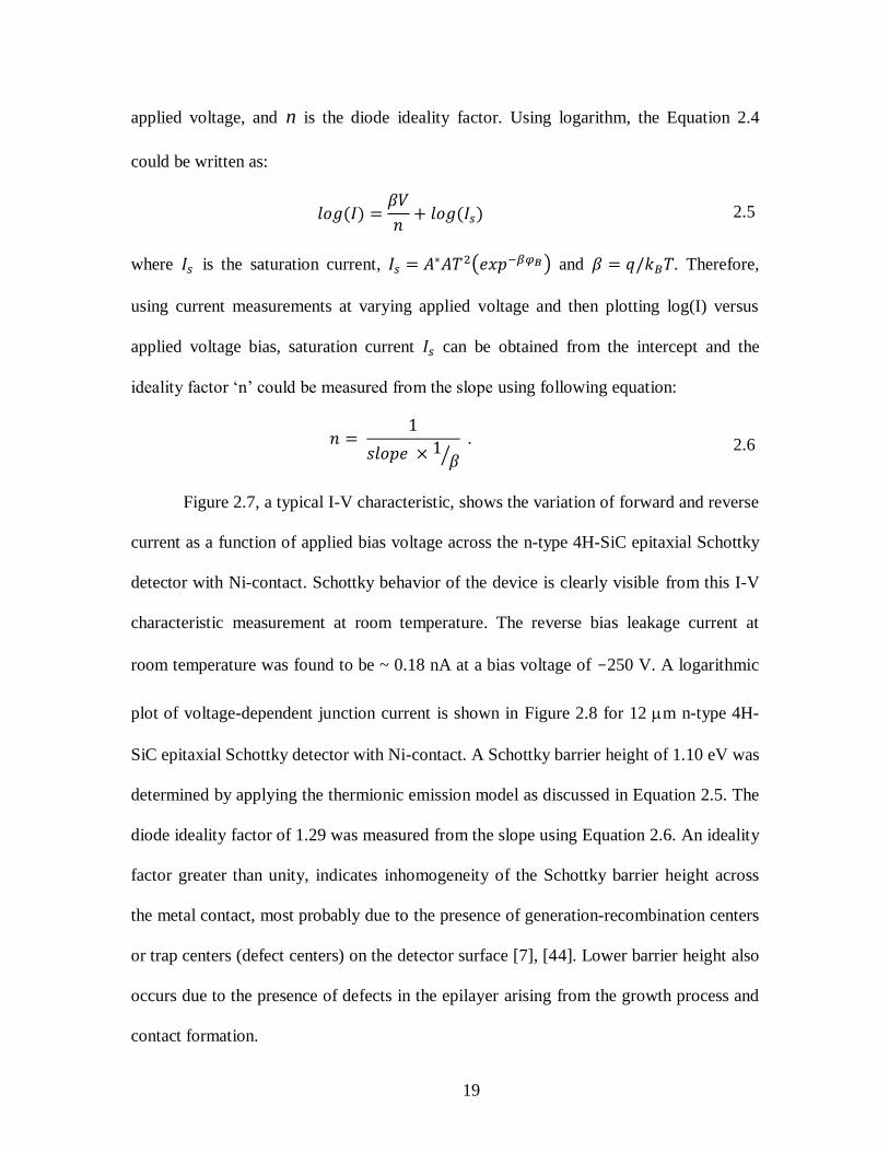
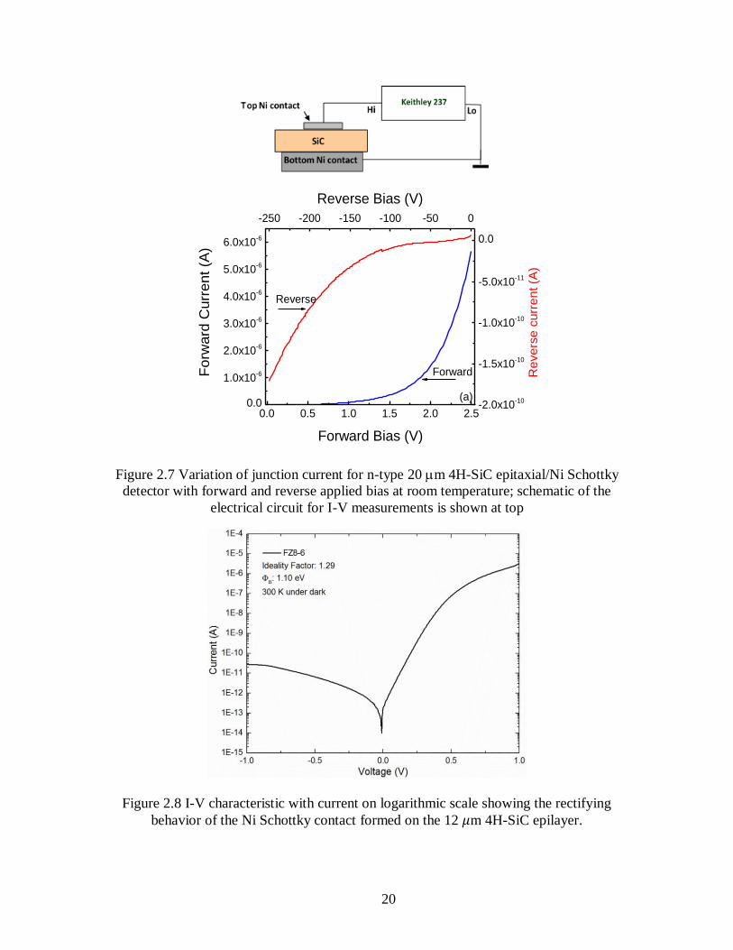
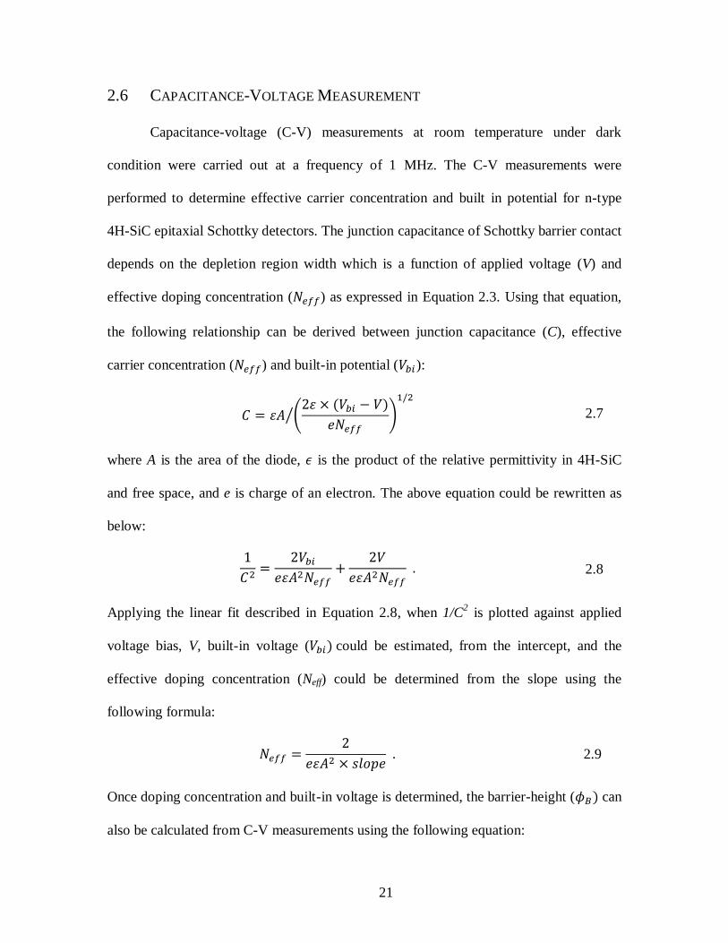


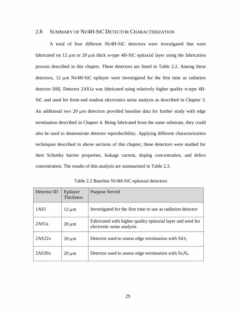


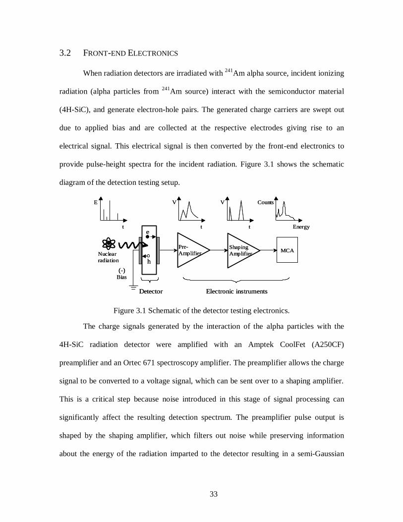

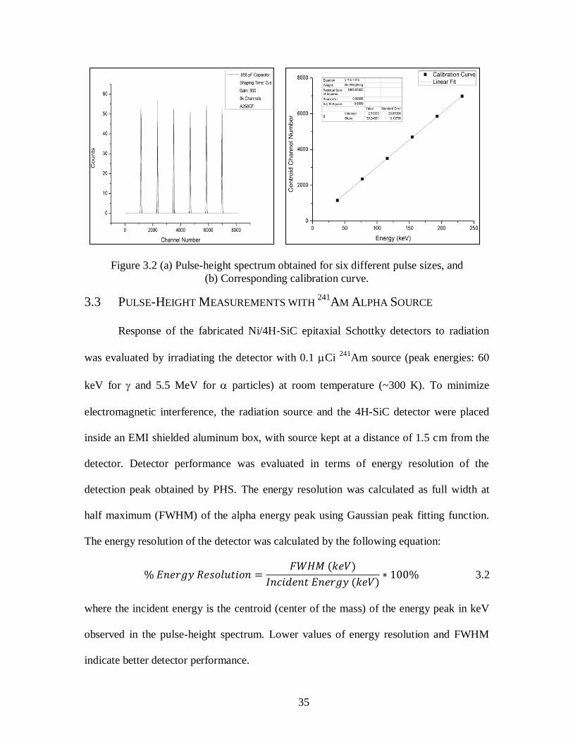


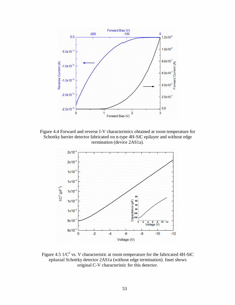


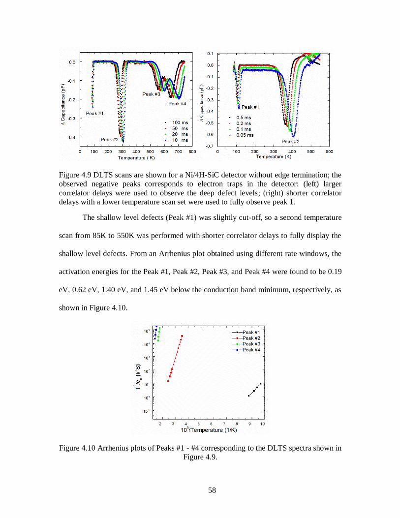


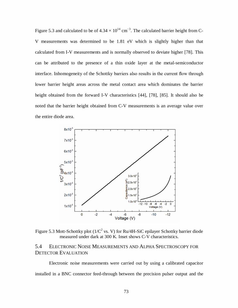


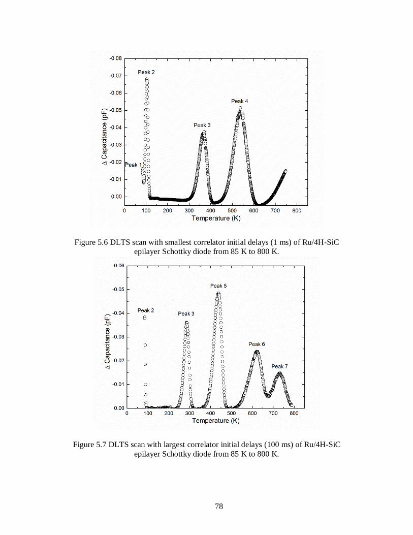


![Chapter 2 SiC Materials and Processing Technology€¦ · 34 2 SiC Materials and Processing Technology Table 2.1 Key electrical parameters of SiC [1] Property 4H-SiC 6H-SiC 3C-SiC](https://static.fdocuments.us/doc/165x107/5f4fd11797ddad63bf719816/chapter-2-sic-materials-and-processing-technology-34-2-sic-materials-and-processing.jpg)


