IMPROVED ERA AMPLIFIERS (AN-60-010) - UC …long/ece145a/Lab2_145A/BiasingMMICAmps.pdfIMPROVED ERA...
23
AN-60-010 Rev.: E (07/12/01) M77554 File: AN60010.DOC Page 1 OF 23 This document and its contents are the property of Mini-Circuits. IMPROVED ERA AMPLIFIERS (AN-60-010) Introduction The improved Mini-Circuits ERA series of amplifiers offer the RF designer multi-stage performance in a package which looks like a discrete transistor. Improved ERA amplifiers advantages of wide bandwidth, impedance match, and a choice of gain and output power levels result from their being monolithic circuits which contain InGaP HBTs (indium gallium phosphide heterojunction bipolar transistors). Applying DC power to operate an Improved ERA is simpler than biasing a transistor. This article gives the user step-by-step guidance in choosing external bias circuit components to obtain optimum performance. The internal circuit configuration is a Darlington pair, embedded in a resistor network as shown in the schematic diagrams, Figure 1. Like a discrete bipolar transistor, this type of circuit is current- rather than voltage-controlled. This means that for a range of current around a recommended value, the device voltage varies much less than in proportion to current. A constant-current DC source would be ideal for providing a stable operating point. By contrast, if a constant-voltage DC source were used the current would vary widely with small changes in supply voltage, temperature change, and device-to-device variations; such operation is not recommended. Practical applications typically use a series resistor between the Improved ERA and a source of DC voltage to approximate constant current; so, how best to use this technique is a one of the themes of this article. An Improved ERA amplifier is a 2-port device: RF input, and combined RF output and bias input. It has 4 leads including 2 ground leads; connecting both of them to external ground will minimize common path impedance for best RF performance. Internal resistors in Figure 1 determine the DC operating point of the transistors and provide feedback to set RF gain, bandwidth, and input and output impedances to optimum values.
-
Upload
vuongkhanh -
Category
Documents
-
view
215 -
download
2
Transcript of IMPROVED ERA AMPLIFIERS (AN-60-010) - UC …long/ece145a/Lab2_145A/BiasingMMICAmps.pdfIMPROVED ERA...

AN-60-010 Rev.: E (07/12/01) M77554 File: AN60010.DOC Page 1 OF 23This document and its contents are the property of Mini-Circuits.
IMPROVED ERA AMPLIFIERS(AN-60-010)
Introduction
The improved Mini-Circuits ERA series of amplifiers offer the RF designer multi-stageperformance in a package which looks like a discrete transistor. Improved ERAamplifiers advantages of wide bandwidth, impedance match, and a choice of gain andoutput power levels result from their being monolithic circuits which contain InGaPHBTs (indium gallium phosphide heterojunction bipolar transistors).
Applying DC power to operate an Improved ERA is simpler than biasing a transistor.This article gives the user step-by-step guidance in choosing external bias circuitcomponents to obtain optimum performance.
The internal circuit configuration is a Darlington pair, embedded in a resistor networkas shown in the schematic diagrams, Figure 1. Like a discrete bipolar transistor, thistype of circuit is current- rather than voltage-controlled. This means that for a rangeof current around a recommended value, the device voltage varies much less than inproportion to current. A constant-current DC source would be ideal for providing astable operating point. By contrast, if a constant-voltage DC source were used thecurrent would vary widely with small changes in supply voltage, temperature change,and device-to-device variations; such operation is not recommended. Practicalapplications typically use a series resistor between the Improved ERA and a source ofDC voltage to approximate constant current; so, how best to use this technique is a oneof the themes of this article.
An Improved ERA amplifier is a 2-port device: RF input, and combined RF output andbias input. It has 4 leads including 2 ground leads; connecting both of them to externalground will minimize common path impedance for best RF performance. Internalresistors in Figure 1 determine the DC operating point of the transistors and providefeedback to set RF gain, bandwidth, and input and output impedances to optimumvalues.

AN-60-010 Rev.: E (07/12/01) M77554 File: AN60010.DOC Page 2 OF 23This document and its contents are the property of Mini-Circuits.
Figure 1 Schematic Diagram
Bias Circuit
A practical biasing configuration is shown in Figure 2. Bias current is delivered froma voltage supply Vcc through the resistor Rbias and the RF choke (inductor), shown as
RFC in the figure. The resistor reduces the effect of device voltage (Vc) variation onthe bias current by approximating a current source.
Blocking capacitors are needed at the input and output ports. They should be of a typehaving low ESR (effective series resistance), and should have reactance low enoughnot to affect insertion loss or VSWR adversely at low frequency. The blockingcapacitors must be free of parasitic resonance up to the highest operating frequency.Use of a bypass capacitor at the connection to the DC supply is advised to prevent straycoupling to other signal processing components.
Figure 2 Typical biasing Configuration for Improved ERA AmplifiersIn this circuit, DC blocking capacitors are addedat the input port (pin number 1 on the packagedamplifier) and at the output port (pin 3).

AN-60-010 Rev.: E (07/12/01) M77554 File: AN60010.DOC Page 3 OF 23This document and its contents are the property of Mini-Circuits.
Bias current is given by the equation:
Ibias = (Vcc � Vd) � Rbias
Table 1 lists the values of the bias resistor needed with several values of supply voltagefor each of the Improved ERA models. These values take into account the variation ofdevice voltage, both lot-to-lot and with temperature (-45 to 85(C ambient). Also, theyare chosen from the readily available “1%” resistor values. The table lists the powerdissipated by the bias resistor in the 12-volt case, as an example. The greater thedifference between the supply and device voltage, the easier it is to maintain constantoperating conditions; this is discussed in detail later.
The bias current values in Table 1 are the recommended values. The effect on RFperformance and MTTF of using different currents is discussed later in thisApplication Note. Exceeding the maximum current values shown there, however,could cause excessive junction temperature and premature failure. Substantially lowercurrents, while not degrading device reliability, could cause unpredictable RFperformance because of non-optimum internal operating points.

AN-60-010 Rev.: E (07/12/01) M77554 File: AN60010.DOC Page 4 OF 23This document and its contents are the property of Mini-Circuits.
Table 1 Bias Resistor Values for Various Supply Voltages
ImprovedERA
Model
ERA-1 ERA-2 ERA-21 ERA-3 ERA-33 ERA-4 ERA-50 ERA-51 ERA-6
BiasCurrent 40 mA 40 mA 40 mA 35 mA 40 mA 65 mA 60 mA 65 mA 70 mA
DeviceVoltage(nom.)
3.4V 3.5V 3.5V 3.2V 4.3V 4.5V 4.4V 4.5V 4.9V
SupplyVoltage
Bias Resistor (ohms) at Supply Voltage
7 90.9 88.7 88.7 107 69.8 38.3 47.5 40.2 30.18 113 113 113 133 93.1 52.3 63.4 53.6 43.29 137 137 137 162 115 66.5 78.7 68.1 56.2
10 162 162 162 191 140 80.6 95.3 82.5 69.811 187 187 187 221 165 95.3 113 97.6 84.512 215 215 210 249 191 110 127 113 97.613 237 237 237 280 215 127 143 127 11314 261 261 261 309 243 143 162 143 12715 287 287 287 340 267 158 178 158 14016 309 316 316 365 287 174 196 174 15417 332 340 340 392 316 187 210 191 16918 357 365 365 422 340 205 226 205 18219 383 392 392 453 365 221 243 221 19620 412 412 412 475 392 237 261 237 210
Nominaldissip. inResistorfor 12V
0.34 W 0.34 W 0.34 W 0.31 W 0.31 W 0.51 W 0.45 W 0.50 W 0.52 W
Advantage of an RF Choke
The advisability of using an RF choke in series with Rbias is evident from the followinganalysis. Figure 3 shows an equivalent circuit of the output of an Improved ERAamplifier as a current source in parallel with an internal 50-ohm source resistance,loaded by both Rbias and an external 50-ohm load. The current in the 50-ohm load is:
Isource + Rbias � (2 Rbias + 50)
and the loss in power gain relative to not having the output loaded by Rbias is:
20 log [(2 Rbias + 50) � 2 Rbias] dB.
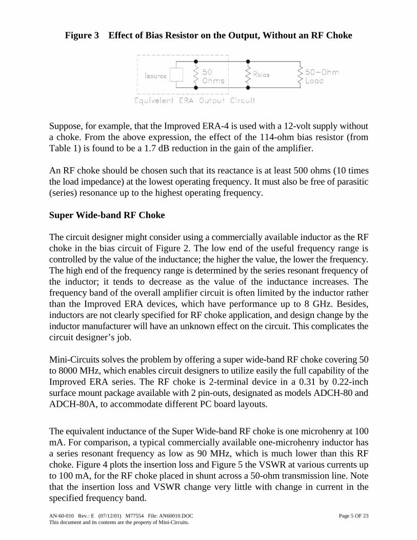
AN-60-010 Rev.: E (07/12/01) M77554 File: AN60010.DOC Page 5 OF 23This document and its contents are the property of Mini-Circuits.
Figure 3 Effect of Bias Resistor on the Output, Without an RF Choke
Suppose, for example, that the Improved ERA-4 is used with a 12-volt supply withouta choke. From the above expression, the effect of the 114-ohm bias resistor (fromTable 1) is found to be a 1.7 dB reduction in the gain of the amplifier.
An RF choke should be chosen such that its reactance is at least 500 ohms (10 timesthe load impedance) at the lowest operating frequency. It must also be free of parasitic(series) resonance up to the highest operating frequency.
Super Wide-band RF Choke
The circuit designer might consider using a commercially available inductor as the RFchoke in the bias circuit of Figure 2. The low end of the useful frequency range iscontrolled by the value of the inductance; the higher the value, the lower the frequency.The high end of the frequency range is determined by the series resonant frequency ofthe inductor; it tends to decrease as the value of the inductance increases. Thefrequency band of the overall amplifier circuit is often limited by the inductor ratherthan the Improved ERA devices, which have performance up to 8 GHz. Besides,inductors are not clearly specified for RF choke application, and design change by theinductor manufacturer will have an unknown effect on the circuit. This complicates thecircuit designer’s job.
Mini-Circuits solves the problem by offering a super wide-band RF choke covering 50to 8000 MHz, which enables circuit designers to utilize easily the full capability of theImproved ERA series. The RF choke is 2-terminal device in a 0.31 by 0.22-inchsurface mount package available with 2 pin-outs, designated as models ADCH-80 andADCH-80A, to accommodate different PC board layouts.
The equivalent inductance of the Super Wide-band RF choke is one microhenry at 100mA. For comparison, a typical commercially available one-microhenry inductor hasa series resonant frequency as low as 90 MHz, which is much lower than this RFchoke. Figure 4 plots the insertion loss and Figure 5 the VSWR at various currents upto 100 mA, for the RF choke placed in shunt across a 50-ohm transmission line. Notethat the insertion loss and VSWR change very little with change in current in thespecified frequency band.

AN-60-010 Rev.: E (07/12/01) M77554 File: AN60010.DOC Page 6 OF 23This document and its contents are the property of Mini-Circuits.
0.1
1
10
INS
ER
TIO
N L
OS
S (
dB)
1 10 100 1000 10000 FREQUENCY (MHz)
0mA 50mA 85mA 100mA
Figure 4 Insertion Loss of the RF Choke
Figure 5 VSWR of the RF Choke
1
10
100
VS
WR
1 10 100 1000 10000 FREQUENCY (MHz)
0mA 50mA 85mA 100mA

AN-60-010 Rev.: E (07/12/01) M77554 File: AN60010.DOC Page 7 OF 23This document and its contents are the property of Mini-Circuits.
Higher Bias Resistor Values Reduce Variation
Increasing the supply voltage allows a higher value of Rbias to be used as shown inTable 1, and that reduces the variation in bias current. The benefit is that RFperformance, especially the 1-dB compression point, is made more constant. Thefollowing quantifies this effect.
The device voltage Vd is a function of both Ibias and temperature T. Device voltageincreases with bias current, and the variation can be expressed as a rate of change
∆ Vd / ∆ Ibias,in mV per mA. Device voltage decreases with increasing temperature, as
∆ Vd / ∆Tmillivolts per degree C. Typical values for these variation coefficients are listed inTable 2 for the Improved ERA devices.
Table 2 Improved ERA Device Voltage Variation with Current andTemperature
Improved ERA
Model No.
Nominal BiasCurrent, mA
Typ. Device VoltageVariation with Current,
∆Vd/∆Ibias (mV/mA)
Typ. Device VoltageVariation with Temperature,
∆Vd/∆T (mV/(C)
ERA-1 40 8.0 - 2.4
ERA-2 40 6.0 -2.5
ERA-21 40 8.7 -2.4
ERA-3 35 3.3 -2.4
ERA-33 40 6.0 -3.5
ERA-4 65 9.3 -2.9
ERA-50 60 5.8 -3.4
ERA-51 65 5.6 -3.2
ERA-6 70 14.0 -3.1
The combined effect of the two device-voltage coefficients can be expressed asvariation of bias current with temperature, derived as follows:
Ibias = [Vcc � Vd(Ibias, T)] � Rbias,
where Vd(Ibias, T) = V0 + (∆ Vd / ∆ Ibias) # Ibias + (∆ Vd / ∆T) # (T � T0)
The $∆# ratios are the coefficients from Table 2. V0 is the Vd-axis intercept of the linearVd vs. Ibias curve, at room temperature T0. Substituting for Vd and solving for Ibias:
Ibias = [Vcc�V0 � (∆ Vd / ∆T) # (T � T0)] � [Rbias + (∆ Vd / ∆ Ibias)]

AN-60-010 Rev.: E (07/12/01) M77554 File: AN60010.DOC Page 8 OF 23This document and its contents are the property of Mini-Circuits.
Differentiating with respect to T gives the desired result:
∆ Ibias / ∆T = �(∆ Vd / ∆T) � [Rbias + (∆ Vd / ∆ Ibias)]
To find the change in bias current that will typically occur with a given change intemperature ∆T, substitute values for the device-voltage coefficients from Table 2, andthe value of bias resistor being considered, into the right-hand side of the equation.Multiplying the result by ∆T yields the change in bias current ∆ Ibias.
To illustrate the effect of supply voltage, let us consider two examples for theImproved ERA-1, based upon Tables 1 and 2. For Vcc = 5 volts and Rbias = 40 ohms,
∆ Ibias / ∆T = �(�2.4) � (40 + 8) = .050 mA/(C.
Over an operating temperature range of �45 to 85 degrees C, the total variation incurrent for this example will be 6.5 mA, which is more than 15% of the recommendedvalue of current. The consequence is about 1.6 dB variation in output power at 1-dBcompression.
For the second example, try Vcc = 12 volts and Rbias = 215 ohms. A similar calculationyields 1.4 mA total variation in current, which causes less than 0.5 dB variation inoutput power.
Additional Sources of Variation
The variation of device voltage as discussed above pertains to an individual device.The specifications include the limits of device voltage that the various Improved ERAmodels must meet. Actual expected unit-to-unit variation is much less than indicatedby those limits, because of the high degree of process control used during manufacture.Therefore, a user can be confident that results obtained when prototyping products thatincorporate Improved ERA that performance will be highly repeatable.
Besides the variation of bias current due to the characteristics of the Improved ERAitself, there are two additional causes that the user might need to consider:
• Available nominal values, tolerance and temperature coefficient of the bias resistor.• Voltage setting error and regulation of the power supply.
Resistors readily available are generally the “1% values”. The nominal values, havingincrements of 2%, could thus differ from the Table 1 values by as much as ±1%. If aresistor having temperature coefficient of 200 ppm/(C is used, it could vary �1.5%over the �45 to 85(C range. The resistance, and correspondingly the bias current,

AN-60-010 Rev.: E (07/12/01) M77554 File: AN60010.DOC Page 9 OF 23This document and its contents are the property of Mini-Circuits.
might therefore be as much as 2.5% different from the desired value in Table 1 due tothese contributions.
Good DC power supplies typically have about 10 mV combined line and loadregulation, and that tends not to be an important factor. However, the tolerance of afixed-voltage supply, or setting accuracy of a field adjustable one might be ±1%. Asan example, consider the Improved ERA-51 being used with a 9-volt supply. Since thenominal device voltage is 4.5 V (half the supply voltage), a 1%, error in supply voltagewould change the current by 0.5%.
The combination of the resistor and power supply variations in the above examplewould cause 2.5% + 0.5% = 3% error in current, which is 2 mA for a nominal valueof 65 mA. Besides, the temperature effect on current in the Improved ERA-51 deviceitself, using the formula under Table 2, is:
∆ Ibias / ∆T = �(�3.2) � (69 + 6.7) = .042 mA/(C.
Relative to the room temperature value, current would change �3 mA withtemperature. The overall combined variation, including the bias resistor and powersupply effects, is �5 mA for this example. A user working within an MTTF or currentconsumption budget who needs to ensure that 65 mA is not exceeded may thereforechoose to design for a nominal value of 60 mA in this example.
Minimizing Power Dissipation
In addition to bias current stability, stability of power dissipation of the Improved ERAdevice is favored by using a high Vcc value. This is because of the negative
temperature coefficient of device voltage Vd. In particular, if Vcc is at least 2 times Vd,then PD, the Improved ERA power dissipation decreases with increasing temperature,as shown by the following analysis:
PD = Vd # Ibias = Vd (Vcc � Vd) � Rbias
Taking the derivative of PD with respect to Vd and setting it equal to zero, we find that
the maximum value of PD occurs when Vd = Vcc � 2. This is illustrated in Figure 6.

AN-60-010 Rev.: E (07/12/01) M77554 File: AN60010.DOC Page 10 OF 23This document and its contents are the property of Mini-Circuits.
Figure 6 Variation of Improved ERA Power Dissipation with Temperature,for Device Voltage Above, and Below, Half the Supply Voltage Value
Let us see what happens to power dissipation in the case of Improved ERA-4 between25 and 85 degrees C, for two values of supply voltage: one less than, and anothergreater than, twice the value of Vd. We will use 65 mA and 4.5 V as the nominal (room
temperature) values of Ibias and Vd.
To find the change in PD, the power dissipation of the Improved ERA amplifier, wemust use the equations for Ibias and Vd with which we started, above, in order toaccount for the interdependence of these quantities as well as temperature.
Ibias = [Vcc � V0 � (∆ Vd / ∆T) # (T � T0)] � [Rbias + (∆ Vd / ∆ Ibias)], as before.
Substituting for Ibias in the Vd equation and solving for Vd:
Vd = [Rbias # V0 + (∆ Vd / ∆ Ibias) # Vcc + Rbias # (∆ Vd / ∆T) # (T � T0)] �
[Rbias + (∆ Vd / ∆ Ibias)]
PD can now obtained as the product of right-hand sides of these two equations. Theconstant V0 is found by subtracting [Ibias + (∆ Vd /∆ Ibias)] from Vd, using the
room-temperature values of Ibias and Vd.
For Vcc = 5.0 V, Rbias = 7.7 ohms. Using the value �2.9mV/(C for the Vd temperaturecoefficient from Table 3 and the above equations, PD increases from .293 watt at 25(Cto .331 watt at 85(C. Considering the thermal resistance of Improved ERA-4 (junction-to-case) of 177(C/W, this increase in power dissipation results in 7(C higher junctiontemperature than if dissipation were constant. The consequence in reliability is a factorof 2 reduction in MTTF.

AN-60-010 Rev.: E (07/12/01) M77554 File: AN60010.DOC Page 11 OF 23This document and its contents are the property of Mini-Circuits.
Now, try Vcc = 12 V, for which Rbias = 115.4 ohms. For this case, PD decreases from.293watt at 25(C to .288 watt at 85(C.
Temperature Compensated Bias Network
An alternative method of biasing the Improved ERA which allows use of lower supplyvoltage while maintaining bias current stability and reducing power dissipation in thebias resistor is to use a temperature compensating bias network in place of the singleresistor Rbias. The network consists of a linear positive-temperature-coefficient chipthermistor in parallel with a regular chip resistor, and should be designed so that itsresistance increases with temperature just enough to make up for the decrease in devicevoltage, causing the Improved ERA current to remain constant.
Commercially available chip thermistors have a very high TCR (temperaturecoefficient of resistance), typically +4500 ppm/°C for the range 51 - 510 ohms. Thetemperature coefficient needed for Rbias is much less than this, and thus achievable byusing the 2-components (resistor and thermistor) in parallel.
We now derive the values of the network components. Let R be the resistance of theregular resistor, and Rt the 25°C resistance of the thermistor.
Let kb be the fractional increase in Rbias needed at the maximum operating temperaturerelative to 25°C: (hot resistance � 25°C resistance) � 25°C resistance.
Let kt be the fractional increase in resistance of the thermistor,
(4500 +10�6) + (maximum operating temperature � 25°C).
Because the resistor and thermistor are in parallel they must satisfy:
Rbias = R#Rt � (R + Rt ) at 25°C, and
(1 + kb) Rbias = R#Rt (1 + kt) � [R + Rt (1 + kt)]at the maximum operating temperature.
Solving these equations yields:
R = Rbias # kt (1 + kb) � ( kt �kb), and Rt = Rbias # kt (1 + kb) � [kb (1 + kt)]
Let us compare simple resistor biasing with the temperature compensating network forbiasing an Improved ERA-6 with a 7.0 V supply. Let Ibias = 70 mA and Vd = 4.9 V (at
25°C), and use the Rbias value 30.1 ohms from Table 1. If we use an ordinary resistor
AN-60-010 Rev.: E (07/12/01) M77554 File: AN60010.DOC Page 12 OF 23This document and its contents are the property of Mini-Circuits.
for Rbias without a thermistor, the current will increase to 74 mA.
Now, we compute the network component values needed to make the current 70 mAat 85°C as well as at 25°C. At 85°C, Vd = 4.9 –(.0031 V/ °C ) + (60°C) = 4.71V, and
Rbias should become 32.7 ohms. Thus, kb = (32.7 � 30.1) � 30.1 = .0864. Also, kt =
(4500 +10�6) + (85° � 25°) = .27. Applying the formulas,
R = 30.1 + .27 (1 + .0864) � ( .27�.0864) = 48.1 ohms
Rt = 30.1 + .27 (1 + .0864) � [.0864 (1 + .27)] = 80.5 ohms
If the thermistors are available only in $5% values#, sufficiently close compensationis obtained by using Rt = 82 ohms and R = 47.5 ohms (for 30.1-ohm parallelequivalent).
For different supply voltages and device operating points different resistor andthermistor values are needed, but the same concept and method can be used. Thebenefit is the ability to keep the device current constant over temperature, therebyavoiding increase in power dissipated in the amplifier and reduction in MTTF.
We have not mentioned the resistance-temperature coefficient of the ordinary resistorin the bias network. The reason is that thick film chip resistors typically have acoefficient of �100 ppm/(C. This is about 2% of the TCR of the thermistor, and doesnot influence the results significantly. A word of caution is due regarding thethermistor, however. Its temperature characteristic is controlled only at 25°C and at75°C. The user should test actual circuit operation at other temperatures of interest.
RF Performance vs. Device Current
Performance characteristics of Improved ERA devices have been evaluated at severalvalues of bias current, to show users what trade-off they may expect against powerconsumption. The testing was done at room (25(C) ambient. Results are summarizedin Table 3. Entries for the recommended values of current are shown in bold type.
The most pronounced effect of changing the current is in output power at 1-dBcompression, and third-order intercept point (IP3). For Improved ERA-1 as anexample, decreasing the current 5 mA from the recommended value decreases theoutput by 1.6 dB, and increasing it 10 mA increases the output by 2.0 dB. The othermodels show the same amount or somewhat less increase in output when used at highercurrent. Taking an average of the four higher power models, decreasing the current 10mA from the recommended value decreases the output by about 1.5 dB; increasing it

AN-60-010 Rev.: E (07/12/01) M76913 File: AN60010.DOC Page 13 OF 23This document and its contents are the property of Mini-Circuits.
10 mA increases the output by about 1 dB. The accompanying graphs show outputpower at 1-dB compression vs. frequency, with current as a parameter. IP3 essentiallytracks these dB changes.
Gain increases only slightly with increasing current: 0.09 dB per 5 mA for -1, -2, and-21 models, and 0.19 and 0.13 dB per 5 mA for the -3 and -33 models respectively.The three highest power models (-4, -51, and –6) change only about 0.04 dB per 5 mA.
Less change occurs in the other characteristics – flatness, VSWR, and noise figure –and in most cases it is insignificant for practical application.
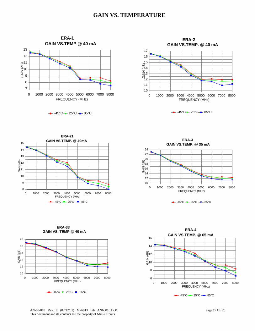
RF Performance vs. Temperature
We also evaluated performance characteristics over the entire operating temperaturerange, �45 to 85(C, at the current recommended in the specifications for each model.Improved ERA-6 was tested at both 65 mA and 70 mA. The results are shown in thelast set of graphs.
At low frequency, data from which the graphs were plotted show that gain of ImprovedERA-33 increases with temperature by 0.23 dB from �45 to 85(C, with slope of+0.0018/(C. Data on all of the other models show 0.12 dB or less variation, and inmost cases gain is maximum around room temperature. At frequencies above 1 GHzthe curves gradually separate, gain decreasing with increasing temperature. Typicallythere is less than 2dB of variation with temperature at 8 GHz.
Output power at 1-dB compression shows very little change with temperature up to 1 or 2 GHz. Itdecreases with increasing temperature at higher frequencies. At 4 GHz for example, the graphs showthat the change ranges from �0.5 dB for Improved ERA-1 to �1.1 dB for Improved ERA-3, at �45and 85(C relative to 25(C. Third-order intercept point (IP3) also generally decreases with increasingtemperature. For the lower power models the graphs show IP3 test results at 2 GHz; for the higherpower models the test frequency is 1 GHz. The temperature effect ranges from �0.5 dB (forImproved ERA-33) up to about �2 dB.
Noise figure increases with increasing temperature. The effect is fairly uniform overthe frequency range up to about 4 GHz, with the curves diverging a little to 8 GHz.There is not much difference in noise figure vs. temperature among the models. At 2GHz for example, total variation over �45 to 85(C ranges from 0.9 to 1.1 dB.

AN-60-010 Rev.: E (07/12/01) M76913 File: AN60010.DOC Page 14 OF 23This document and its contents are the property of Mini-Circuits.
Table 3 Typical Improved ERA Performance at Various Bias Currents
ImprovedERA
Model No.
DeviceCurrent
mA
Gain@2GHz
dB
Flatnessto 2GHz��dB
VSWRIN
@2GHz
VSWROUT
@2GHz
IP3@2GHz
dBm
NoiseFigure, dB
@2GHz
Pout , dBm@1dB Comp.
2GHz35 11.85 0.43 1.43 1.43 25.4 4.5 10.340 11.99 0.44 1.46 1.46 27.9 4.4 11.945 12.06 0.44 1.48 1.47 29.0 4.4 13.2
ERA-1
50 12.11 0.45 1.49 1.48 29.0 4.5 13.935 15.14 0.63 1.45 1.06 26.8 4.0 12.140 15.26 0.63 1.46 1.08 28.3 4.0 13.345 15.34 0.64 1.46 1.09 28.7 4.0 13.5
ERA-2
50 15.40 0.65 1.46 1.11 28.6 4.0 13.735 13.15 0.60 1.11 1.33 26.3 4.0 11.040 13.27 0.63 1.12 1.32 28.3 4.0 12.645 13.35 0.63 1.14 1.33 29.8 4.0 13.6
ERA-21
50 13.43 0.63 1.15 1.34 30.4 4.1 14.325 18.87 1.74 1.68 1.13 23.0 3.2 9.330 19.13 1.83 1.68 1.16 24.8 3.2 11.235 19.26 1.91 1.69 1.17 25.8 3.2 12.5
ERA-3
40 19.40 1.96 1.69 1.21 26.2 3.2 13.135 17.29 0.87 1.82 1.22 27.7 3.9 12.140 17.45 0.89 1.81 1.19 29.9 3.9 13.845 17.52 0.93 1.80 1.17 30.8 3.9 15.0
ERA-33
50 17.68 0.91 1.76 1.16 30.7 4.0 15.8
ImprovedERA
Model No.
DeviceCurrent
mA
Gain@1GHz
dB
Flatnessto 2GHz��dB
VSWRIN
@1GHz
VSWROUT
@1GHz
IP3@1GHz
dBm
NoiseFigure, dB
@1GHz
Pout , dBm@1dB Comp.
1GHz55 14.04 0.44 1.20 1.20 32.5 3.8 16.165 14.13 0.45 1.25 1.20 34.2 3.9 17.470 14.17 0.44 1.22 1.20 34.8 3.9 17.9
ERA-4
80 14.22 0.44 1.23 1.20 34.7 4.0 18.550 19.05 1.7 1.36 1.13 31.1 3.1 15.355 19.13 1.7 1.37 1.15 32.6 3.1 16.360 19.22 1.8 1.38 1.16 34.4 3.1 17.2
ERA-50
65 19.30 1.8 1.39 1.17 35.6 3.1 17.855 17.33 0.84 1.09 1.28 33.6 3.3 16.665 17.45 0.86 1.08 1.26 36.6 3.4 18.170 17.49 0.87 1.09 1.25 37.8 3.4 18.4
ERA-51
80 17.56 0.87 1.09 1.25 37.8 3.5 19.055 12.57 0.23 1.16 1.40 33.3 4.2 16.265 12.66 0.23 1.15 1.39 35.3 4.2 17.570 12.69 0.23 1.15 1.38 35.6 4.3 17.9
ERA-6
80 12.74 0.23 1.14 1.38 35.8 4.3 18.7

AN-60-010 Rev.: E (07/12/01) M76913 File: AN60010.DOC Page 15 OF 23This document and its contents are the property of Mini-Circuits.
6
8
10
12
14
16
OU
TP
UT
PO
WE
R (
dBm
)
0 1000 2000 3000 4000 5000 6000 7000 8000 FREQUENCY (MHz)
35 mA 40 mA 45 mA 50 mA
ERA-1 1dB COMPRESSIONAt 35,40,45,50 mA Bias Currents
POUT VS.CURRENT
2
4
6
8
10
12
14
16
OU
TP
UT
PO
WE
R (
dBm
)
0 1000 2000 3000 4000 5000 6000 7000 8000 FREQUENCY (MHz)
35 mA 40 mA 45 mA 50 mA
ERA-2 1dB COMPRESSIONAt 35,40,45,50 mA Bias Currents
7
8
9
10
11
12
13
14
15
OU
TP
UT
PO
WE
R (
dBm
)
0 1000 2000 3000 4000 5000 6000 7000 8000 FREQUENCY (MHz)
35mA 40mA 45mA 50mA
ERA-21 1dB COMPRESSIONAt 35,40,45,50 mA Bias Currents
2
4
6
8
10
12
14
16
OU
TP
UT
PO
WE
R (
dBm
)
0 1000 2000 3000 4000 5000 6000 FREQUENCY (MHz)
25 mA 30 mA 35 mA 40 mA
ERA-3 1dB COMPRESSIONAt 25,30,35,40 mA Bias Currents
6
8
10
12
14
16
18
OU
TP
UT
PO
WE
R (
dBm
)
0 1000 2000 3000 4000 5000 6000 FREQUENCY (MHz)
35 mA 40 mA 45 mA 50 mA
ERA-33 1dB COMPRESSIONAt 35,40,45,50 mA Bias Currents
2 4 6 8
10 12 14 16 18 20
OU
TP
UT
PO
WE
R (
dBm
)
0 1000 2000 3000 4000 5000 6000 FREQUENCY (MHz)
55 mA 65 mA 70 mA 80 mA
ERA-4 1dB COMPRESSIONAt 55,65,70,80 mA Bias Currents

AN-60-010 Rev.: E (07/12/01) M76913 File: AN60010.DOC Page 16 OF 23This document and its contents are the property of Mini-Circuits.
8
10
12
14
16
18
20
OU
TP
UT
PO
WE
R (
dBm
)
0 1000 2000 3000 4000 5000 6000 FREQUENCY (MHz)
55 mA 65 mA 70 mA 80 mA
ERA-51 1dB COMPRESSIONAt 55,65,70,80 mA Bias Currents
4
6
8
10
12
14
16
18
20
OU
TP
UT
PO
WE
R (
dBm
)
0 1000 2000 3000 4000 5000 6000 FREQUENCY (MHz)
55 mA 65 mA 70 mA 80mA
ERA-6 1dB COMPRESSIONAt 55,65,70,80 mA Bias Currents
10
12
14
16
18
20
OU
TP
UT
PO
WE
R (
dBm
)
0 1000 2000 3000 4000 5000 6000 FREQUENCY (MHz)
55 mA 65 mA 70 mA 80 mA
ERA-50 1dB COMPRESSIONAt 55,65,70,80 mA Bias Currents
POUT VS.CURRENT
AN-60-010 Rev.: E (07/12/01) M76913 File: AN60010.DOC Page 17 OF 23This document and its contents are the property of Mini-Circuits.
7
8
9
10
11
12
13
GA
IN (
dB)
0 1000 2000 3000 4000 5000 6000 7000 8000 FREQUENCY (MHz)
-45°C 25°C 85°C
ERA-1GAIN VS.TEMP @ 40 mA
10
11
12
13
14
15
16
17
GA
IN (
dB)
0 1000 2000 3000 4000 5000 6000 7000 8000 FREQUENCY (MHz)
-45°C 25°C 85°C
ERA-2GAIN VS.TEMP. @ 40 mA
8
9
10
11
12
13
14
15
GA
IN (
dB)
0 1000 2000 3000 4000 5000 6000 7000 8000 FREQUENCY (MHz)
-45°C 25°C 85°C
ERA-21GAIN VS.TEMP. @ 40mA
10
12
14
16
18
20
22
24
GA
IN (
dB)
0 1000 2000 3000 4000 5000 6000 7000 8000 FREQUENCY (MHz)
-45°C 25°C 85°C
ERA-3GAIN VS.TEMP. @ 35 mA
10
12
14
16
18
20
GA
IN (
dB)
0 1000 2000 3000 4000 5000 6000 7000 8000 FREQUENCY (MHz)
-45°C 25°C 85°C
ERA-33GAIN VS. TEMP @ 40 mA
6
8
10
12
14
16
GA
IN (
dB)
0 1000 2000 3000 4000 5000 6000 7000 8000 FREQUENCY (MHz)
-45°C 25°C 85°C
ERA-4GAIN VS.TEMP. @ 65 mA
GAIN VS. TEMPERATURE

AN-60-010 Rev.: E (07/12/01) M76913 File: AN60010.DOC Page 18 OF 23This document and its contents are the property of Mini-Circuits.
7
8
9
10
11
12
13 G
AIN
(dB
)
0 1000 2000 3000 4000 5000 6000 7000 8000 FREQEUNCY (MHz)
-45°C 25°C 85°C
ERA-6GAIN VS. TEMP. @ 70 mA
8
9
10
11
12
13
GA
IN (
dB)
0 1000 2000 3000 4000 5000 6000 7000 8000 FREQUENCY (MHz)
-45°C 25°C 85°C
ERA-6GAIN VS.TEMP @ 65 mA
10
12
14
16
18
20
22
GA
IN (
dB)
0 1000 2000 3000 4000 5000 6000 7000 8000 FREQUENCY (MHz)
-45°C 25°C 85°C
ERA-50GAIN VS.TEMP @ 65 mA
8
10
12
14
16
18
20
GA
IN (
dB)
0 1000 2000 3000 4000 5000 6000 7000 8000 FREQUENCY (MHz)
-45°C 25°C 85°C
ERA-51GAIN VS.TEMP. @ 65 mA
GAIN VS. TEMPERATURE

AN-60-010 Rev.: E (07/12/01) M76913 File: AN60010.DOC Page 19 OF 23This document and its contents are the property of Mini-Circuits.
POUT VS. TEMPERATURE
4
6
8
10
12
14
1dB
CO
MP
RE
SS
ION
0 1000 2000 3000 4000 5000 6000 FREQUENCY (MHz)
-45°C 25°C 85°C
ERA-2OUTPUT POWER VS.TEMPERATURE
5
6
7
8
9
10
11
12
13
1dB
CO
MP
RE
SS
ION
0 1000 2000 3000 4000 5000 6000 7000 8000 FREQUENCY (MHz)
-45°C 25°C 85°C
ERA-1OUTPUT POWER VS. TEMPERATURE
6
7
8
9
10
11
12
13
1dB
CO
MP
RE
SS
ION
0 1000 2000 3000 4000 5000 6000 7000 8000 FREQUENCY (MHz)
-45°C 25°C 85°C
ERA-21OUTPUT POWER VS. TEMPERATURE
2
4
6
8
10
12
14
1dB
CO
MP
RE
SS
ION
0 1000 2000 3000 4000 5000 6000 FREQUENCY (MHz)
-45°C 25°C 85°C
ERA-3OUTPUT POWER VS.TEMPERATURE
4
6
8
10
12
14
16
1dB
CO
MP
RE
SS
ION
0 1000 2000 3000 4000 5000 6000 FREQUENCY (MHz)
-45°C 25°C 85°
ERA-33OUTPUT POWER VS.TEMPERATURE
4
6
8
10
12
14
16
18
20
1 dB
CO
MP
RE
SS
ION
0 1000 2000 3000 4000 5000 6000 FREQ. (MHz)
-45°C 25°C 85°C
ERA-4OUTPUT POWER VS. TEMPERATURE

AN-60-010 Rev.: E (07/12/01) M76913 File: AN60010.DOC Page 20 OF 23This document and its contents are the property of Mini-Circuits.
11
12
13
14
15
16
17
18
19
1dB
CO
MP
RE
SS
ION
0 1000 2000 3000 4000 5000 6000 FREQUENCY (MHz)
-45°C 25°C 85°C
ERA-50OUTPUT POWER VS.TEMPERATURE
6
8
10
12
14
16
18
20
1 dB
CO
MP
RE
SS
ION
0 1000 2000 3000 4000 5000 6000 FREQUENCY (MHz)
-45° 25°C 85°C
ERA-51OUTPUT POWER VS. TEMPERATURE
4
6
8
10
12
14
16
18
1dB
CO
MP
RE
SS
ION
0 1000 2000 3000 4000 5000 6000 FREQUENCY (MHz)
-45°C 25°C 85°C
ERA-6OUTPUT POWER VS. TEMPERATURE at 65 mA
4
6
8
10
12
14
16
18
20
1dB
CO
MP
RE
SS
ION
0 1000 2000 3000 4000 5000 6000 FREQUENCY (MHz)
-45°C 25°C 85°C
ERA-6OUTPUT POWER VS.TEMPERATURE at 70 mA
POUT VS. TEMPERATURE

AN-60-010 Rev.: E (07/12/01) M76913 File: AN60010.DOC Page 21 OF 23This document and its contents are the property of Mini-Circuits.
23
24
25
26
27
28
29
30
IP3
(dB
m)
-45° 25° 85°Temp. (°C)
ERA-1 ERA-2 ERA-21 ERA-3 ERA-33
IP3 vs. Temperature @ 2 GHz
32
33
34
35
36
37
IP3
(dB
m)
-45° 25° 85°Temp. (°C)
ERA-4 ERA-50 ERA-51
ERA-6 (65mA) ERA-6 (70mA)
IP3 vs. Temperature @ 1 GHz
IP3 VS. TEMPERATURE

AN-60-010 Rev.: E (07/12/01) M76913 File: AN60010.DOC Page 22 OF 23This document and its contents are the property of Mini-Circuits.
NOISE VS. TEMPERATURE
3
4
5
6
7
8
NO
ISE
FIG
UR
E (
dB)
0 1000 2000 3000 4000 5000 6000 7000 8000 FREQUENCY (MHz)
-45°C 25°C 85°C
ERA-1NOISE FIGURE
3
4
5
6
7
NO
ISE
FIG
UR
E (
dB)
0 1000 2000 3000 4000 5000 6000 7000 8000 FREQUENCY (MHz)
-45°C 25°C 85°C
ERA-2NOISE FIGURE
2
3
4
5
6
7
NO
ISE
FIG
UR
E (
dB)
0 1000 2000 3000 4000 5000 6000 7000 8000 FREQUENCY (MHz)
-45°C 25°C 85°C
ERA-3NOISE FIGURE
3
4
5
6
7
8
NO
ISE
FIG
UR
E (
dB)
0 1000 2000 3000 4000 5000 6000 7000 8000 FREQUENCY (MHz)
-45°C 25°C 85°C
ERA-33NOISE FIGURE
3
4
5
6
7
8
NO
ISE
FIG
UR
E (
dB)
0 1000 2000 3000 4000 5000 6000 7000 8000 FREQUENCY (MHz)
-45°C 25°C 85°C
ERA-21NOISE FIGURE
3
4
5
6
7
8
NO
ISE
FIG
UR
E (
dB)
0 2000 4000 6000 8000 FREQUENCY (MHz)
-45°C 25°C 85°C
ERA-4NOISE FIGURE

AN-60-010 Rev.: E (07/12/01) M76913 File: AN60010.DOC Page 23 OF 23This document and its contents are the property of Mini-Circuits.
3
4
5
6
7
8
NO
ISE
FIG
UR
E (
dB)
0 1000 2000 3000 4000 5000 6000 7000 8000 FREQUENCY (MHz)
-45°C 25°C 85°C
ERA-50NOISE FIGURE
2
3
4
5
6
7
8
NO
ISE
FIG
UR
E (
dB)
0 1000 2000 3000 4000 5000 6000 7000 8000 FREQUENCY (MHz)
-45°C 25°C 85°C
ERA-51NOISE FIGURE
3
4
5
6
7
8
NO
ISE
FIG
UR
E (
dB)
0 2000 4000 6000 8000 FREQUENCY (MHz)
-45°C 25°C 85°C
ERA-6NOISE FIGURE
3
4
5
6
7
8
NO
ISE
FIG
UR
E (
dB)
0 2000 4000 6000 8000 FREQUENCY (MHz)
-45°C 25°C 85°C
ERA-6 at 70 mANOISE FIGURE
NOISE VS. TEMPERATURE