Implications of Using Lead-Free Solders on X-ray ...Implications of Using Lead-Free Solders on X-ray...
5
Implications of Using Lead-Free Solders on X-ray Inspection of Flip Chips and BGAs David Bernard, Dage Precision Industries Inc. Fremont, CA 94538 e-mail: [email protected] Abstract All contract manufacturers (CM) of printed wiring boards (PWBs) are having to consider their approach to using lead- free solders to meet current, and future, environmental, legislative and market demands. As these lead-free solders have markedly different operating parameters from those of the tried and tested lead-containing solders, the opportunity for production problems rises. Therefore, the application of appropriate test and inspection procedures now becomes even more important to ensuring product quality and reliability. However, the test and inspection equipment, and methods, used for decades may not now be appropriate for this new challenge. This may be because, at worst, some test parameters are no longer valid with the lead-free solders, or, less seriously, the inspection control settings must be varied to accept revised test responses based on acceptable levels for these new materials. Implementing lead-free solder into production, therefore, raises questions as to the acceptability and adequacy of a company’s existing test methods. This paper discusses the implications of using x-ray inspection on lead-free versions of flip chips and BGAs. Introduction Driven by the concerns for the environmental impact of increasing amounts of lead containing products within waste landfill sites, there is now legislative and commercial pressure on OEMs to implement lead-free solutions within the printed circuit boards (PCBs) of their products. As contract manufacturers (CMs) charged with supplying these OEMs, it is therefore becoming evermore necessary to consider implementing a lead-free strategy within production and to decide what effects this change from traditional lead solders will have on the manufacturing and test and inspection procedures that are used. Japan is already well advanced in converting their PCB manufacturing to using lead-free alternatives and expects to have completed the switch by the end of 2004. In Europe, the European Union has set the date of July 2006 for compliance by all member states, which includes the newest, mainly former Eastern Bloc members, as well as the existing 15 countries. In the US, in contrast, no formal date for a transfer to lead-free production has been raised. Therefore, whilst supply to the home market may not require any switch for the forseeable future, the danger of not implementing lead-free into a CMs manufacturing capability could result in their being excluded from supplying into the ‘lead-free’ markets. It should be noted, however, that although there is a legislative timetable for Europe to be lead-free, there are still many European CMs that have yet to implement this capability. Those CMs that have already changed have been through the extended learning curve that the new process profiles for these lead- free solders require. As such, there is much information available to help new lead-free adopters avoid some of the pitfalls experienced so far. Further information on the European lead-free roadmap together with other useful data based on experience of manufacturers moving to lead-free can be found in the web sites in references 1 and 2. Traditional solders have been of the Tin/Lead (Sn/PB) variety and many decades of experience has been invested into using these materials to the best advantage. This has defined the process windows within which to produce PCBs and also shaped the inspection and testing regimes that have been implemented to ensure quality manufacture. In particular, the reflow temperature profile used within surface mount technology production has been defined around the, typically, 183°C liquidus temperature of these solders. In addition, the visual look of the Sn/Pb solder after reflow has been used by experienced operators to confirm the quality of their solder joints. When using lead-free solders, these fundamental indices are completely changed and therefore the underlying tenets that have been established for so long in PCB manufacture may no longer be valid. Lead-free Solders The most commonly used Sn/Pb solders have consisted of around 63% Sn and 37% Pb. The most commonly used lead- free alternatives are the, so called, SAC alloys which are named after the mixture of tin (Sn), silver (Ag) and copper (Cu) that they contain. Although different solders from different suppliers have varying elemental ratios, the SAC alloys all contain around 97% tin. There are other lead-free solders that are available, with other elemental compositions, but, once again, their main constituent is Sn. So, in general, the lead is being replaced by tin in these new solders. The immediate effect of this change is to dramatically increase the liquidus temperature of these solders to around 215 – 230°C. As a result, the reflow oven
Transcript of Implications of Using Lead-Free Solders on X-ray ...Implications of Using Lead-Free Solders on X-ray...
Implications of Using Lead-Free Solderson X-ray Inspection of Flip Chips and BGAs
David Bernard, Dage Precision Industries Inc.Fremont, CA 94538 e-mail: [email protected]
Abstract
All contract manufacturers (CM) of printed wiring boards(PWBs) are having to consider their approach to using lead-free solders to meet current, and future, environmental,legislative and market demands. As these lead-free soldershave markedly different operating parameters from those ofthe tried and tested lead-containing solders, the opportunityfor production problems rises. Therefore, the application ofappropriate test and inspection procedures now becomeseven more important to ensuring product quality andreliability. However, the test and inspection equipment, andmethods, used for decades may not now be appropriate forthis new challenge. This may be because, at worst, some testparameters are no longer valid with the lead-free solders, or,less seriously, the inspection control settings must be variedto accept revised test responses based on acceptable levelsfor these new materials. Implementing lead-free solder intoproduction, therefore, raises questions as to the acceptabilityand adequacy of a company’s existing test methods. Thispaper discusses the implications of using x-ray inspection onlead-free versions of flip chips and BGAs.
Introduction
Driven by the concerns for the environmental impact ofincreasing amounts of lead containing products within wastelandfill sites, there is now legislative and commercialpressure on OEMs to implement lead-free solutions withinthe printed circuit boards (PCBs) of their products. Ascontract manufacturers (CMs) charged with supplying theseOEMs, it is therefore becoming evermore necessary toconsider implementing a lead-free strategy withinproduction and to decide what effects this change fromtraditional lead solders will have on the manufacturing andtest and inspection procedures that are used.
Japan is already well advanced in converting their PCBmanufacturing to using lead-free alternatives and expects tohave completed the switch by the end of 2004. In Europe,the European Union has set the date of July 2006 forcompliance by all member states, which includes thenewest, mainly former Eastern Bloc members, as well as theexisting 15 countries. In the US, in contrast, no formal datefor a transfer to lead-free production has been raised.Therefore, whilst supply to the home market may notrequire any switch for the forseeable future, the danger of
not implementing lead-free into a CMs manufacturingcapability could result in their being excluded fromsupplying into the ‘lead-free’ markets. It should be noted,however, that although there is a legislative timetable forEurope to be lead-free, there are still many European CMsthat have yet to implement this capability. Those CMs thathave already changed have been through the extendedlearning curve that the new process profiles for these lead-free solders require. As such, there is much informationavailable to help new lead-free adopters avoid some of thepitfalls experienced so far. Further information on theEuropean lead-free roadmap together with other useful databased on experience of manufacturers moving to lead-freecan be found in the web sites in references 1 and 2.
Traditional solders have been of the Tin/Lead (Sn/PB)variety and many decades of experience has been investedinto using these materials to the best advantage. This hasdefined the process windows within which to produce PCBsand also shaped the inspection and testing regimes that havebeen implemented to ensure quality manufacture. Inparticular, the reflow temperature profile used withinsurface mount technology production has been definedaround the, typically, 183°C liquidus temperature of thesesolders. In addition, the visual look of the Sn/Pb solder afterreflow has been used by experienced operators to confirmthe quality of their solder joints. When using lead-freesolders, these fundamental indices are completely changedand therefore the underlying tenets that have beenestablished for so long in PCB manufacture may no longerbe valid.
Lead-free Solders
The most commonly used Sn/Pb solders have consisted ofaround 63% Sn and 37% Pb. The most commonly used lead-free alternatives are the, so called, SAC alloys which arenamed after the mixture of tin (Sn), silver (Ag) and copper(Cu) that they contain. Although different solders fromdifferent suppliers have varying elemental ratios, the SACalloys all contain around 97% tin. There are other lead-freesolders that are available, with other elementalcompositions, but, once again, their main constituent is Sn.So, in general, the lead is being replaced by tin in these newsolders. The immediate effect of this change is todramatically increase the liquidus temperature of thesesolders to around 215 – 230°C. As a result, the reflow oven
temperatures typically used for SMT production must beraised to a much higher level – around 290°C so as to ensurethe solder reflow will occur. Such higher temperatures thenbring into question the viability of the components used andbare boards themselves. For example, to be lead-free, astandard tin/lead HASL finish would no longer be permitted.Although there is a lead-free HASL finish that comprises ofa tin/copper/nickel combination. A silver board finish isoften suggested for lead-free because of its bondingproperties with the copper pads. Organic solderableprotector (OSP) and gold board finishes may also beconsidered for lead-free applications. There is also thequestion of the susceptibility of the components to thisadditional temperature as well as the finish on thecomponent legs (reference 2). Finally, the look of thesesolders after reflow is not the same as that seen in Tin/Leadmeaning the ‘experience’ gained in this area is no longerhelpful in determining problems. In other words, using lead-free is not just simply a question of changing to a highertemperature profile within the reflow oven; board type,finish and component choice all have to be considered. Theimplication of using lead-free solders, therefore, is that anew ‘learning-curve’ has to be climbed with necessaryexperimentation and testing to validate these new processes.However, is the test and inspection equipment typically usedfor process control still valid for these new materials? It hasalready been mentioned that the look and behavior of lead-free solders is different to that of Tin/Lead. Therefore, withoptical inspection techniques, questions must be asked as tothe efficacy of their light sources, software algorithms, etc.,for inspecting lead-free materials. In a similar vein, willexisting and new x-ray systems be able to cope? With thedramatic increase in the use of BGA and CSP componentsthis question becomes more ever more important as only x-rays can inspect where optical systems cannot. To ensurethat x-ray inspection remains valid for lead-free applicationsand understanding of the technique is required.
X-ray Inspection
Two dimensional (2-D) x-ray inspection systems, systemmost commonly used within the PCB industry, are basicallyx-ray shadow micrographs (see figure 1). The techniquedemands that an x-ray light source (called an x-ray tube)produces x-rays, within which the sample is bathed. Thediffering materials within the sample absorb more, or less,of the x-ray radiation depending on their density and atomicnumber and cast a shadow of that material at the detector.The denser the material, then the darker the shadow. In thisway, solder and copper tracks appear dark compared withthe laminated circuit board in a PCB, for example. Thedetector converts the incident x-rays into optical images forthe operator to view. The closer the sample is moved to the
x-ray tube then the larger the shadow becomes and this ishow magnification is achieved.
The quality of the x-ray radiation produced by the x-raytube, and its effectiveness as discriminating the differentmaterials within a sample to produce a useful analyticalimage, are defined by the tube settings used. These settingsare called the x-ray tube accelerating voltage, or kV, and thetube power and are used to set the tube at appropriate levelsso as to get a good contrast image at the detector.The accelerating potential is the applied voltage between theanode and cathode of the x-ray tube that makes electrons,produced at the cathode, strike the target anode, creating x-rays. The tube power is calculated from the product of theaccelerating potential and the filament current within thecathode used to produce the electrons. The more power thenthe brighter the x-ray source. However, there are technicallimitations on the maximum power that the tubes canachieve (see references 3 and 4).
The kV is also a measure of the penetrating power of the x-rays. The higher the kV used then the more penetrating arethe resultant x-rays. This means that higher kVs need to beused to image dense, or thick but relatively less dense,objects. At lower kVs, only thin and less dense samples canbe inspected. Otherwise, the x-rays have insufficientpenetrating power to travel through the sample and strike thedetector, so creating the image.
The interaction between penetrating radiation and matter,such as x-rays passing through a sample under test, is not asimple relationship and is based on a number of factors.Further detailed information on this matter can be found inreference 5. However, the important consideration, as far asimaging lead-free solders, is that absorption of the radiationincreases with atomic number and density of the materialthat is present. Table 1 shows the differences in the atomicnumber (Z) and the density between the different elementscontained within lead and lead-free solders. Lead has a veryhigh Z value and this is being replaced in the lead-freematerials mainly with additional quantities of tin that has amuch lower Z value as well as a lower density. Therefore,
Figure 1: Basic 2-D x-ray system configuration
the effect of imaging lead-free solders using the same tubeparameters that would currently be used for traditional leadsolders may result in the image being overexposed. This isbecause the lower Z / less dense materials in the lead-freematerial will absorb the x-rays less, allowing more to passthrough to the detector and potentially saturate it.
Element Lead Tin Silver Copper
Symbol Pb Sn Ag Cu
AtomicNumber (Z)
82 50 47 29
AtomicMass (amu)
207.2 118.71 107.8682 63.546
No. ofProtons
82 50 47 29
No. ofNeutrons
125 69 61 35
Density(g/cm3)
11.34 7.31 10.5 8.96
Table 1: Comparison of fundamental properties ofelements used in lead and lead-free solders
To compensate for this effect, it may be necessary todecrease the tube kV and/or the power values that have beenused previously for x-ray inspection of the lead version.This will ensure that suitably contrasted images are stillavailable for making analysis. However, these changes, ifindeed are needed at all, are likely to be small in quantity.Values of around 5 – 15 kV less accelerating voltage thanfor the equivalent lead soldered board may be the typicaladjustment necessary. The tube power might need to bedecreased by 0.25W but this will be dependent on the x-raysystem being used because of the variation in tubeefficiency, capability and brightness from manufacturer tomanufacturer. Whilst it may be necessary to adjust the x-raytube parameters for lead-free application, most modern x-ray systems have the ability to make comprehensive contrastadjustments to the captured x-ray images – see reference3.Therefore, the changes in contrast that using lead-freesolders might cause compared to previous lead versions maybe able to be adjusted electronically without the need tochange the tube parameters and so simplifying the need tochange test and inspection procedures as lead-free processesare adopted.
Results
The key requirements of x-ray inspection of PCBs, lead-freeor otherwise, is that opens, bridges, shorts, voids, etc. can beseen such that process and production quality control can be
maintained during PCB manufacture. As can be seen in thex-ray images below (images 1 – 8) of lead-free examples ofBGA and CSP investigations, there is sufficient contrast andresolution to be able to clearly identify the faults that mayoccur. Many of these x-ray images come from the results ofthe SMART Group Lead-Free Hands on Experience thatwas held during Nepcon UK 2003 and were produced onDage x-ray inspection systems. At this event, the same PCBwith four different finishes had components placed andreflowed, either by vapour phase or convection, using aSAC (tin./silver/copper) lead-free solder. Furtherinformation and results of using these differentcombinations can be found in reference 6.
Conclusion
Changing to a lead-free process requires a consideration ofthe implications that these new materials have on PCBmanufacture and test / inspection because of their differingproperties to what has been the convention for tin/leadsolders for so many years. The lead-free learning curve hasto be climbed requiring trials to be made and errors willoccur. However, as far as x-ray inspection is concerned thenexisting and future x-ray equipment will be able to see thesefaults under lead-free BGA and CSPs as well as within therest of the SMT components. All that may be necessary isthe adjustment of certain x-ray tube parameters to ensure thebest image contrast is available to allow for easy analysis.
References
(1) www.lead-free.org; www.smartgroup.org;www.leadfreesoldering.com
(2) Report MATC (A) 141: Code of Practice for the Use ofElectronic Components and PCBs in Lead-FreeProcessing, by M. Wickham, A. Brewin, L. Zou & C.P.Hunt, United Kingdom National Physical Laboratoryavailable from www.npl.co.uk
(3) X-ray tube selection criteria for BGA / CSP X-rayinspection, D. Bernard, published in The Proceedings ofSMTA International Conference, Chicago, September2002
(4) Selection Criteria for X-ray Inspection Systems for BGAand CSP Solder Joint Analysis, D. Bernard, published inThe Proceedings of Nepcon Shanghai 2003
(5) www.ndt−ed.org/EducationResources/CommunityCollege/Radiography/Physics/radmatinteraction.htm
(6) For the results of the SMART Group Lead-Free Hands OnExperience held during Nepcon UK, June 2003 seewww.smartgroup.org/ev_leadfree3.asp
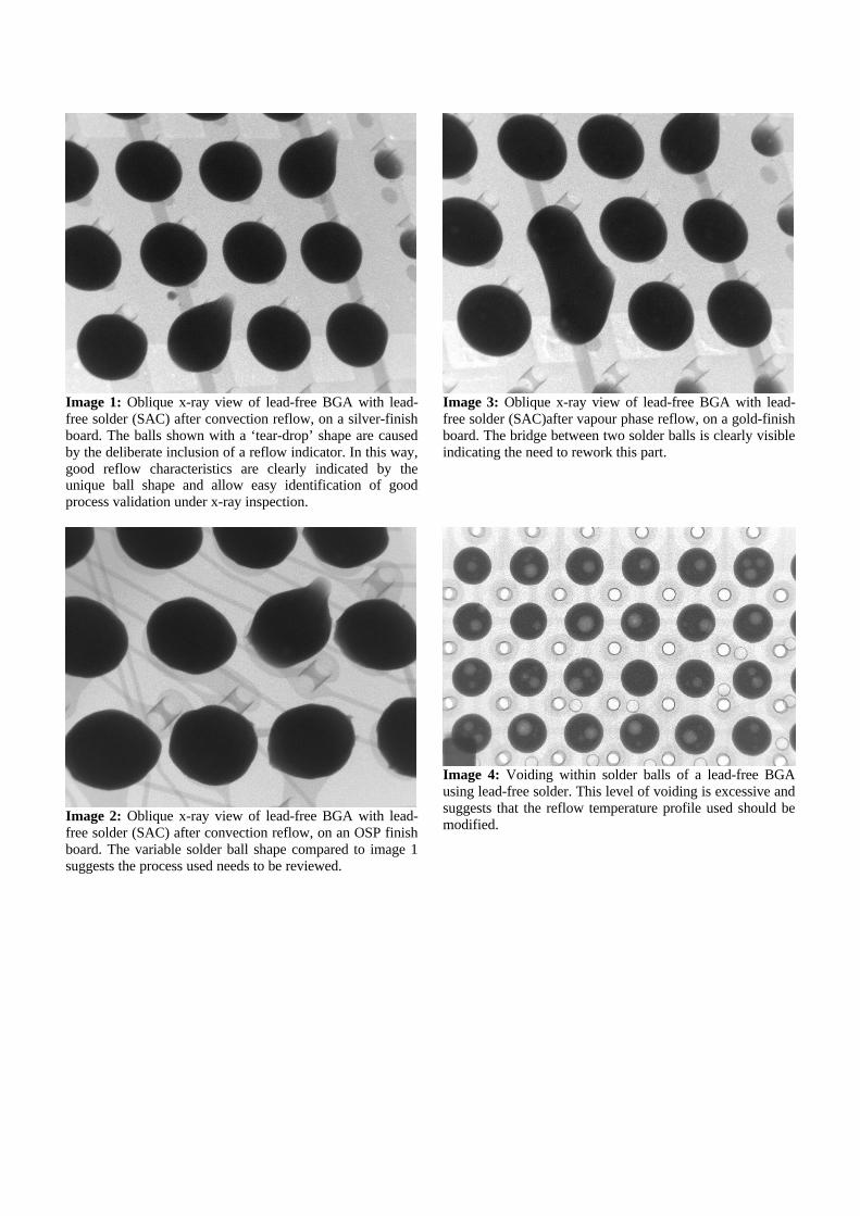
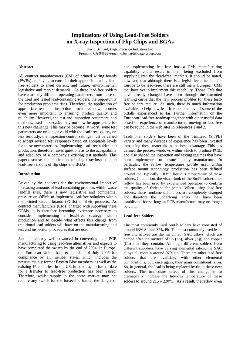
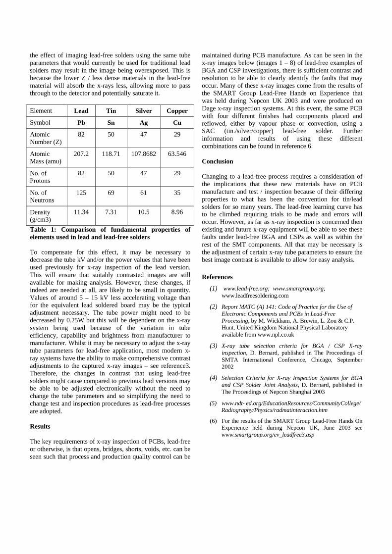
Image 1: Oblique x-ray view of lead-free BGA with lead-free solder (SAC) after convection reflow, on a silver-finishboard. The balls shown with a ‘tear-drop’ shape are causedby the deliberate inclusion of a reflow indicator. In this way,good reflow characteristics are clearly indicated by theunique ball shape and allow easy identification of goodprocess validation under x-ray inspection.
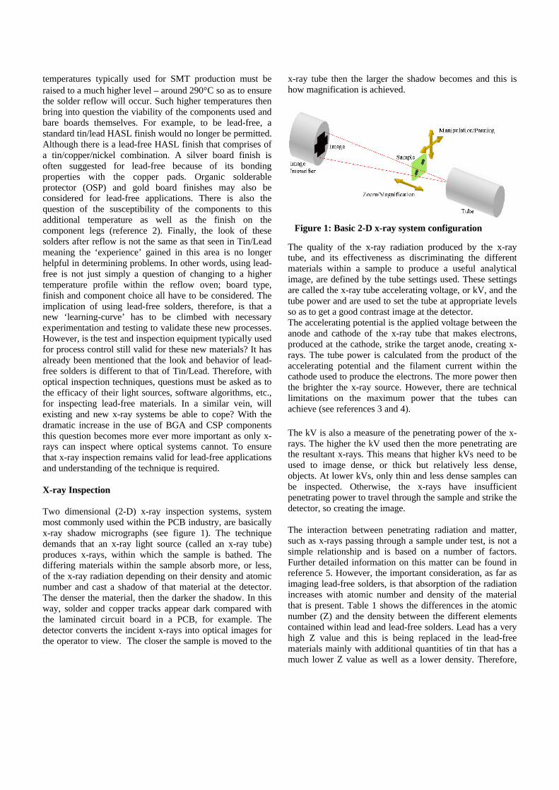
Image 2: Oblique x-ray view of lead-free BGA with lead-free solder (SAC) after convection reflow, on an OSP finishboard. The variable solder ball shape compared to image 1suggests the process used needs to be reviewed.
Image 3: Oblique x-ray view of lead-free BGA with lead-free solder (SAC)after vapour phase reflow, on a gold-finishboard. The bridge between two solder balls is clearly visibleindicating the need to rework this part.
Image 4: Voiding within solder balls of a lead-free BGAusing lead-free solder. This level of voiding is excessive andsuggests that the reflow temperature profile used should bemodified.
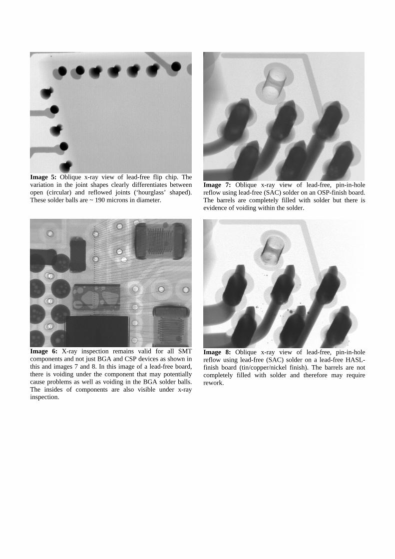
Image 5: Oblique x-ray view of lead-free flip chip. Thevariation in the joint shapes clearly differentiates betweenopen (circular) and reflowed joints (‘hourglass’ shaped).These solder balls are ~ 190 microns in diameter.
Image 6: X-ray inspection remains valid for all SMTcomponents and not just BGA and CSP devices as shown inthis and images 7 and 8. In this image of a lead-free board,there is voiding under the component that may potentiallycause problems as well as voiding in the BGA solder balls.The insides of components are also visible under x-rayinspection.
Image 7: Oblique x-ray view of lead-free, pin-in-holereflow using lead-free (SAC) solder on an OSP-finish board.The barrels are completely filled with solder but there isevidence of voiding within the solder.
Image 8: Oblique x-ray view of lead-free, pin-in-holereflow using lead-free (SAC) solder on a lead-free HASL-finish board (tin/copper/nickel finish). The barrels are notcompletely filled with solder and therefore may requirerework.