
Implication logic gates using spin-transfer-torque ... · Implication logic gates using...
7
Implication logic gates using spin-transfer-torque-operated magnetic tunnel junctions for intrinsic logic-in-memory Hiwa Mahmoudi ⇑ , Thomas Windbacher, Viktor Sverdlov, Siegfried Selberherr Institute for Microelectronics, Technische Universität Wien, Gußhausstraße 27-29/E360, A-1040 Wien, Austria article info Article history: Available online 15 March 2013 Keywords: Logic-in-memory Material implication (IMP) Magnetic tunnel junction (MTJ) Non-volatile logic Spin-transfer torque (STT) abstract As the feature size of CMOS components scales down, the standby power losses due to high leakage cur- rents have become a top concern for modern circuit design. Introducing non-volatility in logic circuits allows to overcome the standby power issue. Magnetic tunnel junctions (MTJs) offer a great potential, because of their non-volatility, unlimited endurance, CMOS compatibility, and fast switching speed. This work proposes current- and voltage-controlled MTJ-based implication (IMP) logic gtes for future non-vol- atile logic-in-memory architecture. The MTJ-based implication logic realizes an intrinsic logic-in-memory known as ‘‘stateful’’ logic for which the MTJ devices serve simultaneously as memory elements and logic gates. Spintronic implication logic gates are analyzed by using a SPICE model for spin-transfer torque (STT) MTJs in order to show the reliability of the IMP operation. It has been demonstrated that the pro- posed current-controlled implication gate offers a higher performance (power and reliability) than the conventional voltage-controlled one. The realization of the spintronic stateful logic operations extends non-volatile electronics from memory to logical computing applications and opens the door for more complex logic functions to be realized with MTJ-based devices. We present a stateful logic circuit based on the common STT-MRAM architecture capable of performing material implication. As an application example, an IMP-based implementation of a full-adder is presented. Ó 2013 Elsevier Ltd. All rights reserved. 1. Introduction The basic structure of a magnetic tunnel junction (MTJ) consists of two ferromagnetic layers separated by a non-conductive tunnel- ing barrier as shown in Fig. 1a. The magnetization of one layer is pinned (fixed layer), while the magnetization of the second one can be switched freely (free layer) using an external magnetic field or the spin-transfer torque (STT) effect [1,2]. In the STT-operated MTJ (STT-MTJ), the spin-polarized electrons induce torque directly on the magnetization of the free layer to enforce switching. There- fore, the STT-MTJ gives pure electrical switching and better scala- bility than conventional MTJs switched by magnetic field. Because of the non-volatility, unlimited endurance, fast-switch- ing speed, and CMOS compatibility of the MTJ devices [3–5], MTJ- based non-volatile logic has received great interest to overcome the significant increase in the leakage currents in CMOS-based cir- cuits [6]. Furthermore, MTJ-based logic can improve the conven- tional CMOS-based logic which combines logic units and memory units to transfer back and forth information between separated lo- gic and memory units, by shortening the interconnection delay and opens the door for a shift away from the Von Neumann architec- ture for innovation in computational paradigms. However, in the previously proposed MTJ-based logic-in-memory and CMOS/MTJ hybrid circuits [7,8], the MTJs are distributed over CMOS logic ele- ments only as ancillary devices for data storage (memory). These architectures require readout schemes for reading the stored logi- cal data as well as providing the next logic stage with properly ad- justed current or voltage signal levels. Furthermore, as the computations are localized, the generalization of the common lo- gic-in-memory circuits to large-scale logic systems is challenging. Here, by using two different circuit topologies of the STT-MTJ- based implication (IMP) gates (Fig. 1b and c), we show the realiza- tion of an intrinsic logic-in-memory architecture (also known as ‘‘stateful’’ logic [9]) for which the MTJ devices are used simulta- neously as the memory elements and the main computing ele- ments (logic gates). Therefore, MTJ-based stateful logic reduces the device counts by eliminating the need for MOS-based logic ele- ments as compared to the common logic architecture. 2. MTJ-Based implication logic gates analysis Material implication, p IMP q, is a fundamental Boolean logic operation which reads ‘p implies q’ or ‘if p, then q’, and is equiva- lent to ‘(NOT p) OR q’ as shown in Table 1. To compute any Boolean 0038-1101/$ - see front matter Ó 2013 Elsevier Ltd. All rights reserved. http://dx.doi.org/10.1016/j.sse.2013.02.017 ⇑ Corresponding author. E-mail addresses: [email protected] (H. Mahmoudi), Windbacher@ iue.tuwien.ac.at (T. Windbacher), [email protected] (V. Sverdlov), Selber [email protected] (S. Selberherr). Solid-State Electronics 84 (2013) 191–197 Contents lists available at SciVerse ScienceDirect Solid-State Electronics journal homepage: www.elsevier.com/locate/sse
Transcript of Implication logic gates using spin-transfer-torque ... · Implication logic gates using...

Solid-State Electronics 84 (2013) 191–197
Contents lists available at SciVerse ScienceDirect
Solid-State Electronics
journal homepage: www.elsevier .com/locate /sse
Implication logic gates using spin-transfer-torque-operated magnetic tunneljunctions for intrinsic logic-in-memory
Hiwa Mahmoudi ⇑, Thomas Windbacher, Viktor Sverdlov, Siegfried SelberherrInstitute for Microelectronics, Technische Universität Wien, Gußhausstraße 27-29/E360, A-1040 Wien, Austria
a r t i c l e i n f o a b s t r a c t
Article history:Available online 15 March 2013
Keywords:Logic-in-memoryMaterial implication (IMP)Magnetic tunnel junction (MTJ)Non-volatile logicSpin-transfer torque (STT)
0038-1101/$ - see front matter � 2013 Elsevier Ltd. Ahttp://dx.doi.org/10.1016/j.sse.2013.02.017
⇑ Corresponding author.E-mail addresses: [email protected] (H
iue.tuwien.ac.at (T. Windbacher), [email protected]@iue.tuwien.ac.at (S. Selberherr).
As the feature size of CMOS components scales down, the standby power losses due to high leakage cur-rents have become a top concern for modern circuit design. Introducing non-volatility in logic circuitsallows to overcome the standby power issue. Magnetic tunnel junctions (MTJs) offer a great potential,because of their non-volatility, unlimited endurance, CMOS compatibility, and fast switching speed. Thiswork proposes current- and voltage-controlled MTJ-based implication (IMP) logic gtes for future non-vol-atile logic-in-memory architecture. The MTJ-based implication logic realizes an intrinsic logic-in-memoryknown as ‘‘stateful’’ logic for which the MTJ devices serve simultaneously as memory elements and logicgates. Spintronic implication logic gates are analyzed by using a SPICE model for spin-transfer torque(STT) MTJs in order to show the reliability of the IMP operation. It has been demonstrated that the pro-posed current-controlled implication gate offers a higher performance (power and reliability) than theconventional voltage-controlled one. The realization of the spintronic stateful logic operations extendsnon-volatile electronics from memory to logical computing applications and opens the door for morecomplex logic functions to be realized with MTJ-based devices. We present a stateful logic circuit basedon the common STT-MRAM architecture capable of performing material implication. As an applicationexample, an IMP-based implementation of a full-adder is presented.
� 2013 Elsevier Ltd. All rights reserved.
1. Introduction
The basic structure of a magnetic tunnel junction (MTJ) consistsof two ferromagnetic layers separated by a non-conductive tunnel-ing barrier as shown in Fig. 1a. The magnetization of one layer ispinned (fixed layer), while the magnetization of the second onecan be switched freely (free layer) using an external magnetic fieldor the spin-transfer torque (STT) effect [1,2]. In the STT-operatedMTJ (STT-MTJ), the spin-polarized electrons induce torque directlyon the magnetization of the free layer to enforce switching. There-fore, the STT-MTJ gives pure electrical switching and better scala-bility than conventional MTJs switched by magnetic field.
Because of the non-volatility, unlimited endurance, fast-switch-ing speed, and CMOS compatibility of the MTJ devices [3–5], MTJ-based non-volatile logic has received great interest to overcomethe significant increase in the leakage currents in CMOS-based cir-cuits [6]. Furthermore, MTJ-based logic can improve the conven-tional CMOS-based logic which combines logic units and memoryunits to transfer back and forth information between separated lo-gic and memory units, by shortening the interconnection delay and
ll rights reserved.
. Mahmoudi), [email protected] (V. Sverdlov), Selber
opens the door for a shift away from the Von Neumann architec-ture for innovation in computational paradigms. However, in thepreviously proposed MTJ-based logic-in-memory and CMOS/MTJhybrid circuits [7,8], the MTJs are distributed over CMOS logic ele-ments only as ancillary devices for data storage (memory). Thesearchitectures require readout schemes for reading the stored logi-cal data as well as providing the next logic stage with properly ad-justed current or voltage signal levels. Furthermore, as thecomputations are localized, the generalization of the common lo-gic-in-memory circuits to large-scale logic systems is challenging.
Here, by using two different circuit topologies of the STT-MTJ-based implication (IMP) gates (Fig. 1b and c), we show the realiza-tion of an intrinsic logic-in-memory architecture (also known as‘‘stateful’’ logic [9]) for which the MTJ devices are used simulta-neously as the memory elements and the main computing ele-ments (logic gates). Therefore, MTJ-based stateful logic reducesthe device counts by eliminating the need for MOS-based logic ele-ments as compared to the common logic architecture.
2. MTJ-Based implication logic gates analysis
Material implication, p IMP q, is a fundamental Boolean logicoperation which reads ‘p implies q’ or ‘if p, then q’, and is equiva-lent to ‘(NOT p) OR q’ as shown in Table 1. To compute any Boolean

Fig. 1. (a) MTJ basic structure. The conventional [9] (voltage-controlled) implica-tion gate, (b) and our proposed (current-controlled) implication gate, (c) circuittopologies.
192 H. Mahmoudi et al. / Solid-State Electronics 84 (2013) 191–197
function, the operations IMP and NIMP (negated IMP) form a com-putationally complete logic basis in combination with any opera-tion from the sets C and C0, respectively, for which C = {NOT,FALSE, XOR, NIMP} and C0 = {NOT, TRUE, XNOR, IMP}.
To enable memristive stateful logic operations, the realizationof the operation IMP has been demonstrated recently [9] usingTiO2 memristive switches [10]. However, the TiO2-based IMP offerslow speed and requires a different fabrication platform than theexisting cost-effective silicon process. In contrast to [9], we useMTJs as the memory elements to build spintronic IMP gates. Inaddition to the conventional (voltage-controlled) IMP circuit topol-ogy (Fig. 1b), we propose and investigate a new topology (Fig. 1c)driven by a current source (current-controlled IMP), which offers amore energy-efficient and reliable implementation.
The electrical resistance of the device depends on the relativeorientation of the magnetization directions of the ferromagneticlayers as shown in Fig. 1a. The parallel (P) magnetization state re-sults in a low resistance state (LRS; RP) across the barrier, while theantiparallel (AP) alignment places it in a high-resistance state(HRS; RAP). The resistance modulation is described by the tunnelmagnetoresistance (TMR) ratio, defined as TMR = (RAP � RP)/RP. Asa non-volatile memory element, the MTJ can store binary logic datavia its low and high resistance states.
In the voltage-controlled topology (Fig. 1b), the material impli-cation can be executed by simultaneously applying the voltagepulses Vcond and Vset to the source MTJ (Mp) and the target MTJ(Mq) for which |Vcond| < |Vset|. According to the polarities, thesevoltage pulses tend to put the MTJs in a low resistance state. Inthe current-controlled topology the material implication can beexecuted by applying the current pulse Iimp as shown in Fig. 1c.In this topology the source MTJ is connected to a conventionalresistance (RG) while the target MTJ (Mq) is connected to theground directly. The current pulse Iimp is in a direction which tendsto put the MTJs in a low resistance state.
Table 1The material implications, IMP and NIMP (negated IMP), truth tables.
State p q p IMP q p NIMP q
1 0 0 1 02 0 1 1 03 1 0 0 14 1 1 1 0
In both voltage- and current-controlled topologies, dependingon the initial resistance states of the source and the target MTJs,a high-to-low resistance switching event is enforced to the targetMTJ (desired switching event) or not (undesired switching event).In fact, a desired switching event is a high-to-low switching eventwhich is enforced to Mq only, when both Mp and Mq are initially athigh resistance states (State 1) and for all three other possible com-binations of the initial resistance states (States 2, 3, and 4), theresistance states of Mp and Mq are left unchanged and there is noundesired switching event as shown in Table 2. This conditionalswitching behavior corresponds to the basic Boolean operationscalled material implications, IMP and NIMP. The initial logic stateof the source and target MTJs act as the inputs, while the final logicstate of the target MTJ is the output of the logic operation. In com-bination with the writing operation (low-to-high resistanceswitching), the material implication forms a complete logic basisto compute an arbitrary Boolean function.
Indeed, as shown in Table 2, if we define the high and low resis-tance states (HRS and LRS) as logical 1 and 0, respectively, the real-ized conditional switching behavior will be equivalent to the logicoperation NIMP for which the result of qn NIMP pn will be writteninto the target device Mq. Here the variables p and q indicate thelogical state of the Mp and Mq, respectively. With this definition,the low-to-high resistance switching is equivalent to writing logi-cal 1 (operation TRUE). In combination with TRUE, the operationNIMP forms a complete logic basis to compute any Booleanfunction.
Opposite to the conventional definition, if we define the highand low resistance states as HRS � 0 and LRS � 1, the realizedconditional switching will be equivalent to the fundamentalBoolean logic operation IMP as qn+1 pn IMP qn. With this defi-nition, the low-to-high resistance switching is equivalent towriting logical 0 (operation FALSE). In combination with FALSE,the operation IMP forms a complete logic basis to computeany Boolean function.
We analyze the implication gates based on the SPICE model ofthe MTJ [11], which uses the equivalent circuit of the STT-MTJshown in Fig. 2. A curve-fitting circuit is used to model the volt-age-dependent effective TMR, which is important to determinethe R–V characteristics of the MTJ and the voltage (current) divi-sion between the source and target MTJs in an implication gate.In this SPICE model the output signals of the decision circuit (V1
and V2) are used to determine that when the device should switchstates based on the critical switching time and current (s0 and IC0))characteristics of the device, which are usually defined correspond-ing to the 50% switching probability. However, the decision signalV1 does not fit the experimental data equally well as shown inFig. 3. Therefore, in order to estimate the MTJ switching character-istics and analyze the logic behavior and the reliability of theimplication gates, we have extended the SPICE model by introduc-ing an error calculation circuit shown in Fig. 2. The theoreticalexpression of the MTJ switching probability (Psw in Eq. (1)) [13]which has been experimentally verified in [12], is now reproducedwell with our extended model as shown in Fig. 3.
Psw ¼ 1� exp � ts0
exp �D0 1� IIC0
� �� �� �ð1Þ
Here D0 is the magnetic memorizing energy without any cur-rent and magnetic field, t is the pulse width, and I is the currentflowing through the MTJ. We therefore use the proposed improvedSPICE model for direct calculation of Psw and an implication reli-ability analysis.
For reliability analysis, according to Table 2, we define theimplication error as:
Eimp ¼ ð1� Pq1swÞ þ Pp1
sw þ Pp2sw þ Pq3
sw ð2Þ
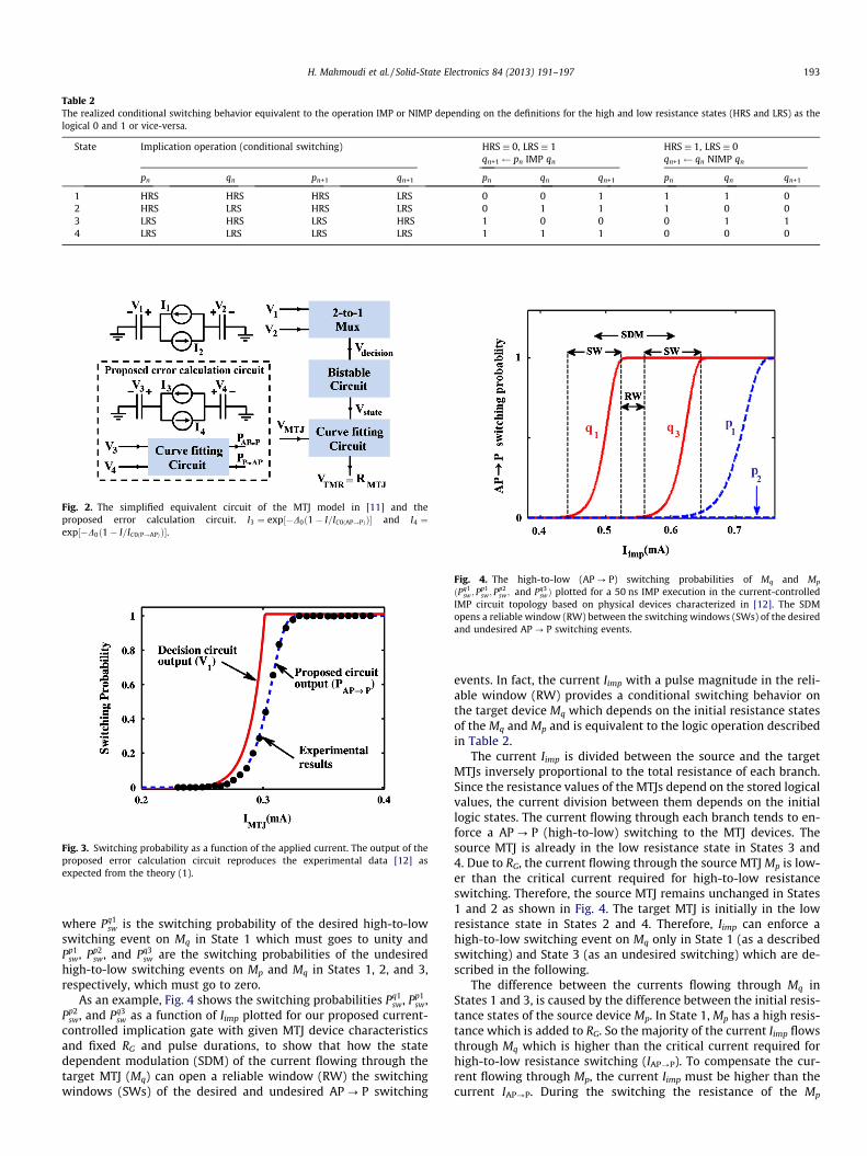
Table 2The realized conditional switching behavior equivalent to the operation IMP or NIMP depending on the definitions for the high and low resistance states (HRS and LRS) as thelogical 0 and 1 or vice-versa.
State Implication operation (conditional switching) HRS � 0, LRS � 1 HRS � 1, LRS � 0qn+1 pn IMP qn qn+1 qn NIMP qn
pn qn pn+1 qn+1 pn qn qn+1 pn qn qn+1
1 HRS HRS HRS LRS 0 0 1 1 1 02 HRS LRS HRS LRS 0 1 1 1 0 03 LRS HRS LRS HRS 1 0 0 0 1 14 LRS LRS LRS LRS 1 1 1 0 0 0
Fig. 2. The simplified equivalent circuit of the MTJ model in [11] and theproposed error calculation circuit. I3 ¼ exp½�D0ð1� I=IC0ðAP!PÞÞ� and I4 ¼exp½�D0ð1� I=IC0ðP!APÞÞ�.
Fig. 3. Switching probability as a function of the applied current. The output of theproposed error calculation circuit reproduces the experimental data [12] asexpected from the theory (1).
Fig. 4. The high-to-low (AP ? P) switching probabilities of Mq and Mp
ðPq1sw; P
p1sw; P
p2sw; and Pq3
swÞ plotted for a 50 ns IMP execution in the current-controlledIMP circuit topology based on physical devices characterized in [12]. The SDMopens a reliable window (RW) between the switching windows (SWs) of the desiredand undesired AP ? P switching events.
H. Mahmoudi et al. / Solid-State Electronics 84 (2013) 191–197 193
where Pq1sw is the switching probability of the desired high-to-low
switching event on Mq in State 1 which must goes to unity andPp1
sw, Pp2sw, and Pq3
sw are the switching probabilities of the undesiredhigh-to-low switching events on Mp and Mq in States 1, 2, and 3,respectively, which must go to zero.
As an example, Fig. 4 shows the switching probabilities Pq1sw, Pp1
sw,Pp2
sw, and Pq3sw as a function of Iimp plotted for our proposed current-
controlled implication gate with given MTJ device characteristicsand fixed RG and pulse durations, to show that how the statedependent modulation (SDM) of the current flowing through thetarget MTJ (Mq) can open a reliable window (RW) the switchingwindows (SWs) of the desired and undesired AP ? P switching
events. In fact, the current Iimp with a pulse magnitude in the reli-able window (RW) provides a conditional switching behavior onthe target device Mq which depends on the initial resistance statesof the Mq and Mp and is equivalent to the logic operation describedin Table 2.
The current Iimp is divided between the source and the targetMTJs inversely proportional to the total resistance of each branch.Since the resistance values of the MTJs depend on the stored logicalvalues, the current division between them depends on the initiallogic states. The current flowing through each branch tends to en-force a AP ? P (high-to-low) switching to the MTJ devices. Thesource MTJ is already in the low resistance state in States 3 and4. Due to RG, the current flowing through the source MTJ Mp is low-er than the critical current required for high-to-low resistanceswitching. Therefore, the source MTJ remains unchanged in States1 and 2 as shown in Fig. 4. The target MTJ is initially in the lowresistance state in States 2 and 4. Therefore, Iimp can enforce ahigh-to-low switching event on Mq only in State 1 (as a describedswitching) and State 3 (as an undesired switching) which are de-scribed in the following.
The difference between the currents flowing through Mq inStates 1 and 3, is caused by the difference between the initial resis-tance states of the source device Mp. In State 1, Mp has a high resis-tance which is added to RG. So the majority of the current Iimp flowsthrough Mq which is higher than the critical current required forhigh-to-low resistance switching (IAP?P). To compensate the cur-rent flowing through Mp, the current Iimp must be higher than thecurrent IAP?P. During the switching the resistance of the Mp
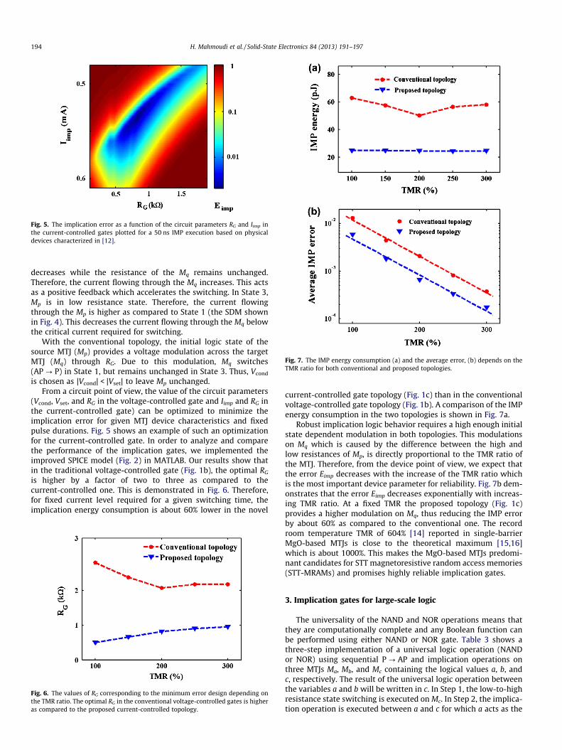
Fig. 5. The implication error as a function of the circuit parameters RG and Iimp inthe current-controlled gates plotted for a 50 ns IMP execution based on physicaldevices characterized in [12].
Fig. 7. The IMP energy consumption (a) and the average error, (b) depends on theTMR ratio for both conventional and proposed topologies.
194 H. Mahmoudi et al. / Solid-State Electronics 84 (2013) 191–197
decreases while the resistance of the Mq remains unchanged.Therefore, the current flowing through the Mq increases. This actsas a positive feedback which accelerates the switching. In State 3,Mp is in low resistance state. Therefore, the current flowingthrough the Mp is higher as compared to State 1 (the SDM shownin Fig. 4). This decreases the current flowing through the Mq belowthe critical current required for switching.
With the conventional topology, the initial logic state of thesource MTJ (Mp) provides a voltage modulation across the targetMTJ (Mq) through RG. Due to this modulation, Mq switches(AP ? P) in State 1, but remains unchanged in State 3. Thus, Vcond
is chosen as |Vcond| < |Vset| to leave Mp unchanged.From a circuit point of view, the value of the circuit parameters
(Vcond, Vset, and RG in the voltage-controlled gate and Iimp and RG inthe current-controlled gate) can be optimized to minimize theimplication error for given MTJ device characteristics and fixedpulse durations. Fig. 5 shows an example of such an optimizationfor the current-controlled gate. In order to analyze and comparethe performance of the implication gates, we implemented theimproved SPICE model (Fig. 2) in MATLAB. Our results show thatin the traditional voltage-controlled gate (Fig. 1b), the optimal RG
is higher by a factor of two to three as compared to thecurrent-controlled one. This is demonstrated in Fig. 6. Therefore,for fixed current level required for a given switching time, theimplication energy consumption is about 60% lower in the novel
Fig. 6. The values of RG corresponding to the minimum error design depending onthe TMR ratio. The optimal RG in the conventional voltage-controlled gates is higheras compared to the proposed current-controlled topology.
current-controlled gate topology (Fig. 1c) than in the conventionalvoltage-controlled gate topology (Fig. 1b). A comparison of the IMPenergy consumption in the two topologies is shown in Fig. 7a.
Robust implication logic behavior requires a high enough initialstate dependent modulation in both topologies. This modulationson Mq which is caused by the difference between the high andlow resistances of Mp, is directly proportional to the TMR ratio ofthe MTJ. Therefore, from the device point of view, we expect thatthe error Eimp decreases with the increase of the TMR ratio whichis the most important device parameter for reliability. Fig. 7b dem-onstrates that the error Eimp decreases exponentially with increas-ing TMR ratio. At a fixed TMR the proposed topology (Fig. 1c)provides a higher modulation on Mq, thus reducing the IMP errorby about 60% as compared to the conventional one. The recordroom temperature TMR of 604% [14] reported in single-barrierMgO-based MTJs is close to the theoretical maximum [15,16]which is about 1000%. This makes the MgO-based MTJs predomi-nant candidates for STT magnetoresistive random access memories(STT-MRAMs) and promises highly reliable implication gates.
3. Implication gates for large-scale logic
The universality of the NAND and NOR operations means thatthey are computationally complete and any Boolean function canbe performed using either NAND or NOR gate. Table 3 shows athree-step implementation of a universal logic operation (NANDor NOR) using sequential P ? AP and implication operations onthree MTJs Ma, Mb, and Mc containing the logical values a, b, andc, respectively. The result of the universal logic operation betweenthe variables a and b will be written in c. In Step 1, the low-to-highresistance state switching is executed on Mc. In Step 2, the implica-tion operation is executed between a and c for which a acts as the

Table 3The realized conditional switching behavior equivalent to the operation IMP or NIMP. The variables cn+2 (a) and cn+3 (b) indicate the target (source) logical values of theimplication operations in Step 2 and Step 3, respectively.
State Three subsequent operation on a, b, c HRS � 0, LRS � 1 HRS � 1, LRS � 0
Input 1: HRS 2: Imp. (a, c) 3: Imp. (b, c) cn+3 a NAND b cn+3 a NOR b
a b cn+1 cn+2 cn+3 a b cn+3 a b cn+3
1 HRS HRS HRS LRS LRS 0 0 1 1 1 02 HRS LRS HRS LRS LRS 0 1 1 1 0 03 LRS HRS HRS HRS LRS 1 0 1 0 1 04 LRS LRS HRS HRS HRS 1 1 0 0 0 1
H. Mahmoudi et al. / Solid-State Electronics 84 (2013) 191–197 195
source variable and c is the target variable. In Step 3, the implica-tion operation is executed between b and c for which b acts as thesource variable and c is the target variable. Therefore, the final re-sult is written in Mc, and Ma and Mb will remain unchanged.
Similar to the operations described in Table 2, if we define thehigh and low resistance states (HRS and LRS) as logical 0 and 1,respectively, the realized universal operation is equivalent to theNAND operation which has been executed in three steps includinga FALSE and two IMP operations. But if we use the opposite defini-tion (HRS � 1 and LRS � 0), the realized operation is equivalent tothe NOR operation which includes a TRUE and two NIMP opera-tions. This example shows that any logic circuit which is designedby using the operations AND, OR, and NOT in the Shannon’s con-ventional logic framework can also be designed by using IMP(NIMP) and FALSE (TRUE) operations.
In order to generalize the MTJ-based implication gates to a largescale logic-in-memory circuit, we use the magnetoresistive ran-dom access memory (MRAM) architecture. In conventional MRAMarchitecture the MTJ is connected to the crossing points of two per-pendicular arrays of parallel conducting lines. The STT switchingtechnique brought significant advantages and eliminates the dif-ference between reading and writing in STT-MRAM architecture[12]. A typical memory cell of the STT-MRAM, which consists ofan access transistor and an MTJ as its storage element (1T/1MTJstructure) is shown in Fig. 8.
Fig. 9 shows simplified implication logic circuit architecturebased on the STT-MRAM architecture to realize the MTJ-based cur-rent-controlled implication gate shown in Fig. 1c. This circuit en-ables MTJ-based stateful logic architecture for which the need ofusing extra charge-based logic gates is eliminated and the memorycells serve simultaneously as logic gates and latches via implica-tion operation.
The implication operation between two memory cells Ci,j and C0i;j(qi;j p0i;j IMP qi,j) can be performed by simultaneous selection ofthe i-th word lines (WLs) and the j-th and the j0-th source line(SL) selectors which connect the SLs to the ground directly and
Fig. 8. 1T/1MTJ structure. Structural (a) and
via RG, respectively, and by applying the current source Iimp tothe j-th and j0-th bit lines (BLs). Then the result of the implicationoperation will be written in Ci,j.
As compared to the STT-MRAM, we have added two work cellsto any WL, while it has been shown that with two additional mem-ristors all Boolean functions on any number of memory cells can beperformed [18]. These work cells can also be used to connect differ-ent WLs. Indeed, in order to perform the implication betweenmemory cells from different WLs, one can copy the logic datastored in one memory cell to a work cell from the other WL. Itshould be noted that the nonzero ON resistance of the access tran-sistors (Ron) decreases the effective TMR of the 1T/1MTJ cells whichcan be defined as:
TMReff ¼RAP � RP
RP þ Ronð3Þ
Therefore, a robust implication operation needs MTJs with suf-ficiently high TMR and electrical resistance. Our simulations showthat the TMR of a 1T/1MTJ including the MTJ devices characterizedin [12] and an access device with a width of about 1–2 lm at the180-nm technology decreases by about 10–30%. Therefore, accord-ing to Fig. 7b, a 99.9% implication correct logic behavior requires aTMR ratio higher than 250%.
3.1. Stateful spintronic full-adder
We consider the implication-based realization of a full-adderwhich is a basic element of arithmetic circuits. As is well known,it adds three binary inputs (q1, q2, and cin) and produces two binaryoutputs, sum (s = q1 XOR q2 XOR cin) and carry (cout = [q1 AND q2]OR [cin AND (q1 XOR q2)]) as shown in Fig. 10. We use the definitionHRS � 0 and LRS � 1, so the basic implication logic operations areequivalent to FALSE and IMP.
Since the implication gates cannot fan out, a logical value whichis required as the target variable for an implication operation hasto be copied in an additional cell, if it is needed as an input for
the equivalent circuit, (b) diagrams [17].

Fig. 9. Simplified spintronic implication logic circuit architecture based on the STT-RAM architecture. Controlling and programming the line drivers and selectorsrequires an external processor similar to the proposed circuit for the TiO2-basedarchitecture [9].
Fig. 10. A logic diagram of a full-adder.
196 H. Mahmoudi et al. / Solid-State Electronics 84 (2013) 191–197
subsequent operations. Therefore, we use the additional cells a1, a2,and a3 to perform two subsequent operations FALSE and IMP, forexample (a1 0 and a1 q1 IMP 0), to write �q1 (NOT q1) in theadditional cell a1 before we use q1 as a target cell. According to(4)–(6), our design involves only 27 subsequent FALSE and IMPoperations on three input cells q1, q2, and cin) and three additionalcells (a1-a3), in contrast to the earlier proposed IMP-based scheme[19] with 19 and 18 operations (37 total) for generating s and cout,respectively, and four additional cells.
fa1 0; q1 IMP a1; a2 0; q2 IMP a2; a1 IMP a2; a3
0; a2 IMP a3; a2
0; q2 IMP a2; a2 IMP a1; a1 IMP a3g � fa3
q1 XOR q2g ð4Þ
fq1 IMP a2; q1 0; a3 IMP q1; cin IMP q1; q2
0; q1 IMP q2; a2 IMP q2g � fq2 coutg ð5Þ
fa1 0; cin IMP a1; q1 0; a3 IMP q1; a1 IMP q1; a1
0; q1 IMP a1; a3 IMP cin; a1 IMP cing � fa3 s
¼ q1 XOR q2 XOR cing ð6Þ
Therefore, our design requires less operations (delay) and de-vices (area). As ‘p IMP 0’ and ‘p IMP q’ are equivalent to ‘NOT p’and ‘(NOT p) OR q’, respectively, some operations can be eliminated
to minimize the total effort. In the logic-in-memory circuit pre-sented in [7], the MTJs are used only as ancillary devices whichstore the result of the logical computations performed by the tran-sistors. Therefore, it requires 34 transistors and four MTJs forimplementing a full-adder, while the stateful architecture usesthe MTJs as the main devices for computations and eliminatesthe need of using extra logic gates and offers superior logic density.
4. Conclusion
We have described MTJ-based implication gates as basic ele-ments which inherently realize a logic-in-memory architecturecalled stateful logic for which the memory and logic computingare combined based on existing STT-MRAM architectures. Thisopens an alternative path towards non-volatile MTJ-based comput-ing devices and systems [20]. The reliability of the IMP operation isbased upon a state dependent modulation (SDM) of the voltage(current) division between the source and target MTJs, which in-creases exponentially with increasing TMR ratio. Due to non-vola-tility and also because of eliminating extra charge-based logicgates, the MTJ-based stateful logic is expected to exhibit low powerconsumption, high logic density, and high speed operationsimultaneously.
Acknowledgment
The work is supported by the European Research Councilthrough the Grant #247056 MOSILSPIN.
References
[1] Slonczewski JC. Current-driven excitation of magnetic multilayers. J MagnMagn Mater 1996;159:L1–7.
[2] Berger L. Emission of spin waves by a magnetic multilayer traversed by acurrent. Phys Rev B Condens Matter 1996;54:9353–8.
[3] Baibich MN, Broto JM, Fert A, van Dau FN, Petro F, Etienne P, et al. Giantmagnetoresistance of (001)Fe/(001)Cr magnetic superlattices. Phys Rev Lett1988;61:2472–5.
[4] Engel BN, Akerman J, Butcher B, Dave RW, DeHerrera M, Durlam M, et al. A 4-Mb toggle MRAM based on a novel bit and switching method. IEEE Trans Magn2005;41:132–6.
[5] Chappert C, Fert A, van Dau FN. The emergence of spin electronics in datastorage. Nature Mater 2007;6:813–23.
[6] Kim NS, Austin T, Baauw D, Mudge T, Flautner K, Hu JS, et al. Leakage current:Moore’s law meets the static power. Computer 2003;36:68–75.
[7] Matsunaga S, Hayakawa J, Ikeda S, Miura K, Endoh T, Ohno H, et al. MTJ-Basednonvolatile logic-in-memory circuit, future prospects and issues. In: Proc desautom test Eur conf (DATE); 2009. p. 433–5.
[8] Gang Y, Zhao W, Klein JO, Chappert C, Mazoyer P. A high-reliability, low-powermagnetic full adder. IEEE Trans Magn 2011;47:4611–6.
[9] Borghetti J, Snider GS, Kuekes PJ, Yang JJ, Stewart DR, Williams RS. ‘Memristive’switches enable ‘stateful’ logic operations via material implication. Nature2010;464:873–6.
[10] Strukov DB, Snider GS, Stewart DR, Williams RS. The missing memristor found.Nature 2008;453:80–3.
[11] Harms JD, Ebrahimi F, Yao XF, Wang JP. SPICE Macromodel of spin-torque-transfer-operated magnetic tunnel junctions. IEEE Trans Electron Dev2010;57:1425–30.
[12] Hosomi M, Yamagishi H, Yamamoto T, Bessho K, Higo Y, Yamane K, et al. Anovel nonvolatile memory with spin torque transfer magnetization switching:spin-RAM. In: IEDM Tech dig; 2005. p. 459–62.
[13] Higo Y, Yamane K, Ohba K, Narisawa H, Besso K, Hosomi M, et al. Thermalactivation effect on spin transfer switching in magnetic tunnel junctions. ApplPhys Lett 2005;87:082502.
[14] Ikeda S, Hayakawa J, Ashizawa Y, Lee YM, Miura K, Hasegawa H, et al. Tunnelmagnetoresistance of 604% at 300 K by suppression of Ta diffusion in CoFeB/MgO/CoFeB pseudo-spin-valves annealed at high temperature. Appl Phys Lett2008;93:082508.
[15] Butler WH, Zhang X-G, Schulthess TC, MacLaren JM. Spin-dependent tunnelingconductance of Fe|MgO|Fe sandwiches. Phys Rev B 2001;63:054416.
[16] Mathon J, Umersky A. Theory of tunneling magnetoresistance of an epitaxialFe/MgO/Fe(0 0 1) junction. Phys Rev B 2001;63:220403.
[17] Li H, Chen Y. An overview of non-volatile memory technology and theimplication for tools and architectures. In: Proc des autom test Eur conf(DATE); 2009. p. 731–6.

H. Mahmoudi et al. / Solid-State Electronics 84 (2013) 191–197 197
[18] Lehtonen E, Poikonen JH, Laiho M. Two memristors suffice to compute allboolean functions. Electron Lett 2010;46:239–40.
[19] Bickersta K, Swartzlander EE. Memristor-based arithmetic. In: Asilomar confon sig sys and comp; 2010. p. 1173–7.
[20] Yao X, Harms J, Lyle A, Ebrahimi F, Zhang Y, Wang JP. Magnetic tunneljunction-based spintronic logic units operated by spin transfer torque. IEEETrans Nanotechnol 2012;11:120–6.


![Gates and Logic: From Transistors to Logic Gates and Logic ......Gates and Logic: From Transistors to Logic Gates and Logic Circuits [Weatherspoon, Bala, Bracy, and Sirer] Prof. Hakim](https://static.fdocuments.us/doc/165x107/5fa95cb6eb1af8231472f381/gates-and-logic-from-transistors-to-logic-gates-and-logic-gates-and-logic.jpg)