Implementing Logic Gates and Circuits Discussion D5.1.
80
Implementing Logic Gates and Circuits Discussion D5.1
-
date post
19-Dec-2015 -
Category
Documents
-
view
224 -
download
4
Transcript of Implementing Logic Gates and Circuits Discussion D5.1.

Implementing Logic Gates and Circuits
Discussion D5.1
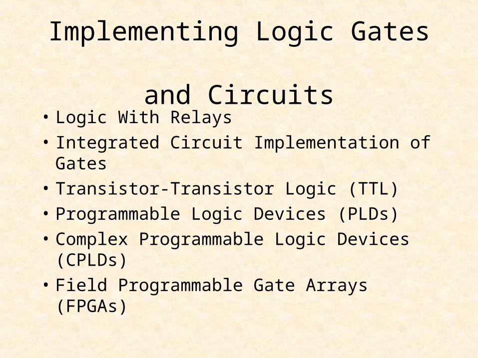
Implementing Logic Gates and Circuits
• Logic With Relays
• Integrated Circuit Implementation of Gates
• Transistor-Transistor Logic (TTL)
• Programmable Logic Devices (PLDs)
• Complex Programmable Logic Devices (CPLDs)
• Field Programmable Gate Arrays (FPGAs)
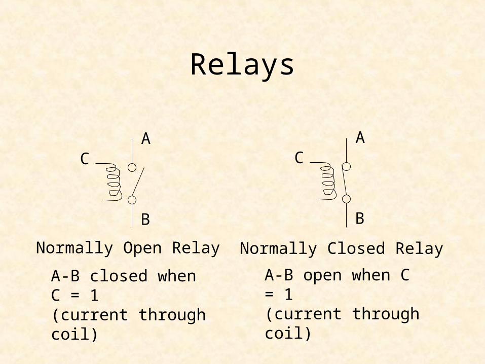
Relays
Normally Open Relay
A
B
CA
B
C
Normally Closed Relay
A-B closed when C = 1(current through coil)
A-B open when C = 1(current through coil)

NOT Gate5V
XY
0 1
closed
openX Y
01
10
X Y
Y
NOTX Y
Y = X’
NOT

NOT Gate5V
X Y01
closed
open
X Y
01
10
X Y
Y
NOTX Y
Y = X’
NOT

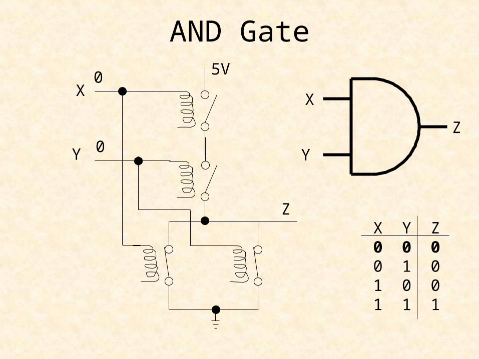
AND Gate
X Y Z0 0 00 1 01 0 01 1 1
X
Y
Z
5V
X
Y
Z
AND Gate
X Y Z0 0 00 1 01 0 01 1 1
X
Y
Z
5V
X
Y
Z
0
0

AND Gate
X Y Z0 0 00 1 01 0 01 1 1
X
Y
Z
0
1
X
Y
Z
5VX
Y
Z
5V
X
Y
Z
5VX
Y
Z
5V
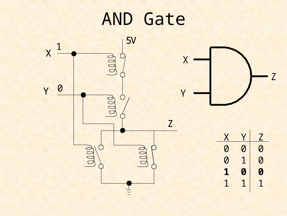
AND Gate
X Y Z0 0 00 1 01 0 01 1 1
X
Y
Z
1
0

AND Gate
X Y Z0 0 00 1 01 0 01 1 1
X
Y
Z
1
1
X
Y
Z
5VX
Y
Z
5V
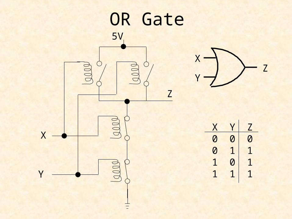
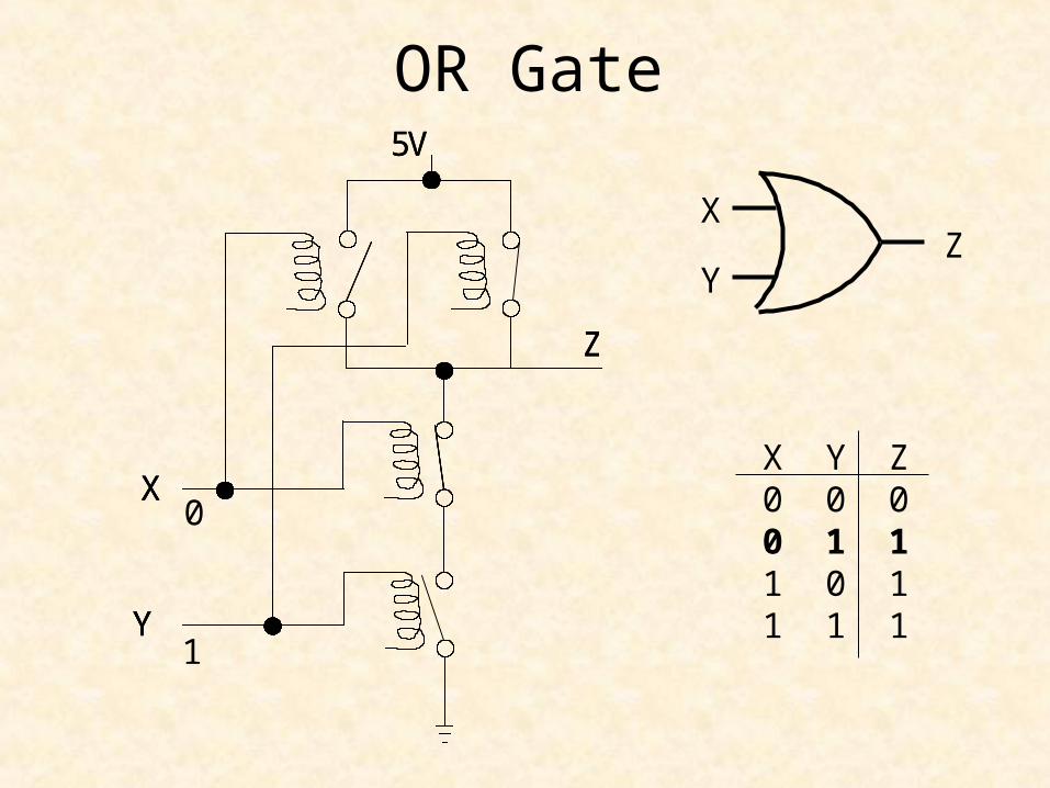
OR Gate
X Y Z0 0 00 1 11 0 11 1 1
5V
X
Y
Z
X
YZ

OR Gate
X Y Z0 0 00 1 11 0 11 1 1
5V
X
Y
Z
X
YZ
0
0
OR Gate
X Y Z0 0 00 1 11 0 11 1 1
X
YZ
0
1
5V
X
Y
Z
5V
X
Y
Z
X
Y
Z

OR Gate
X Y Z0 0 00 1 11 0 11 1 1
X
YZ
1
0
5V
X
Y
Z
5V
X
Y
Z
X
Y
Z

OR Gate
X Y Z0 0 00 1 11 0 11 1 1
X
YZ
1
1
5V
X
Y
Z
5V
X
Y
Z
X
Y
Z

Implementing Gates Using MOSFET Integrated Circuits
Relays
Normally openNormally closed
A
B
C
A
B
C
A
B
C
nMOS transistorA-B closed whenC = 1(normally open)
pMOS transistorA-B closed whenC = 0(normally closed)

NOT Gate5V
X YY = X'
X Y
X Y
01
10

NOT Gate5V
X YY = X'
X Y
0 1
X Y
01
10

NOT Gate5V
X YY = X'
X Y
1 0
X Y
01
10

NAND Gate
X
Y
Z
5V
X
YZ
X Y Z0 0 10 1 11 0 11 1 0

NAND Gate
X
Y
Z
5V
X
YZ
X Y Z0 0 10 1 11 0 11 1 0
0
0
NAND Gate
X
Y
Z
5V
X
YZ
X Y Z0 0 10 1 11 0 11 1 0
0
1
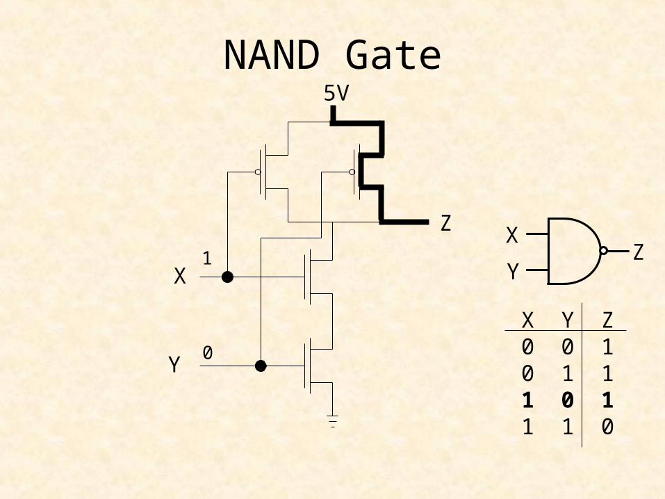
NAND Gate
X
Y
Z
5V
X
YZ
X Y Z0 0 10 1 11 0 11 1 0
1
0
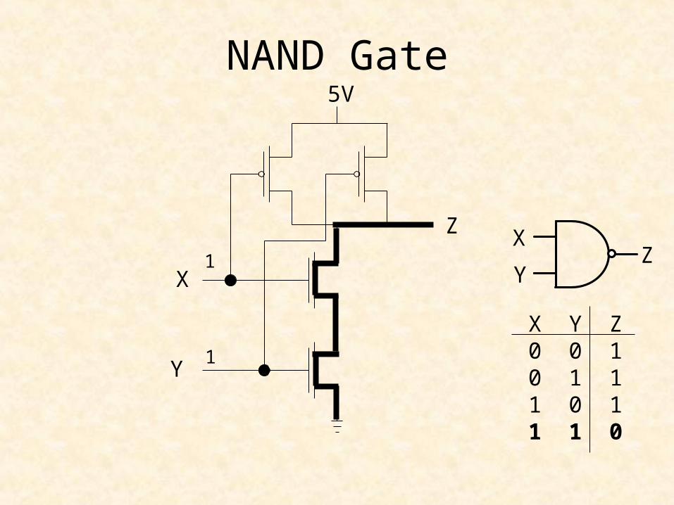
NAND Gate
X
Y
Z
5V
X
YZ
X Y Z0 0 10 1 11 0 11 1 0
1
1
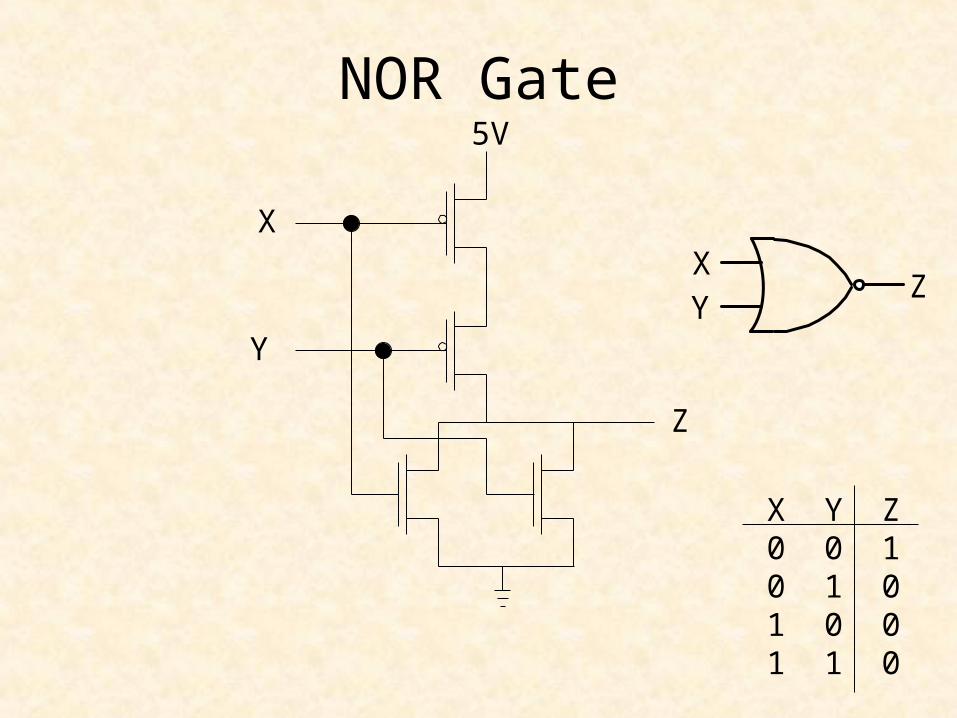
NOR Gate
X
Y
Z
5V
XY
Z
X Y Z0 0 10 1 01 0 01 1 0

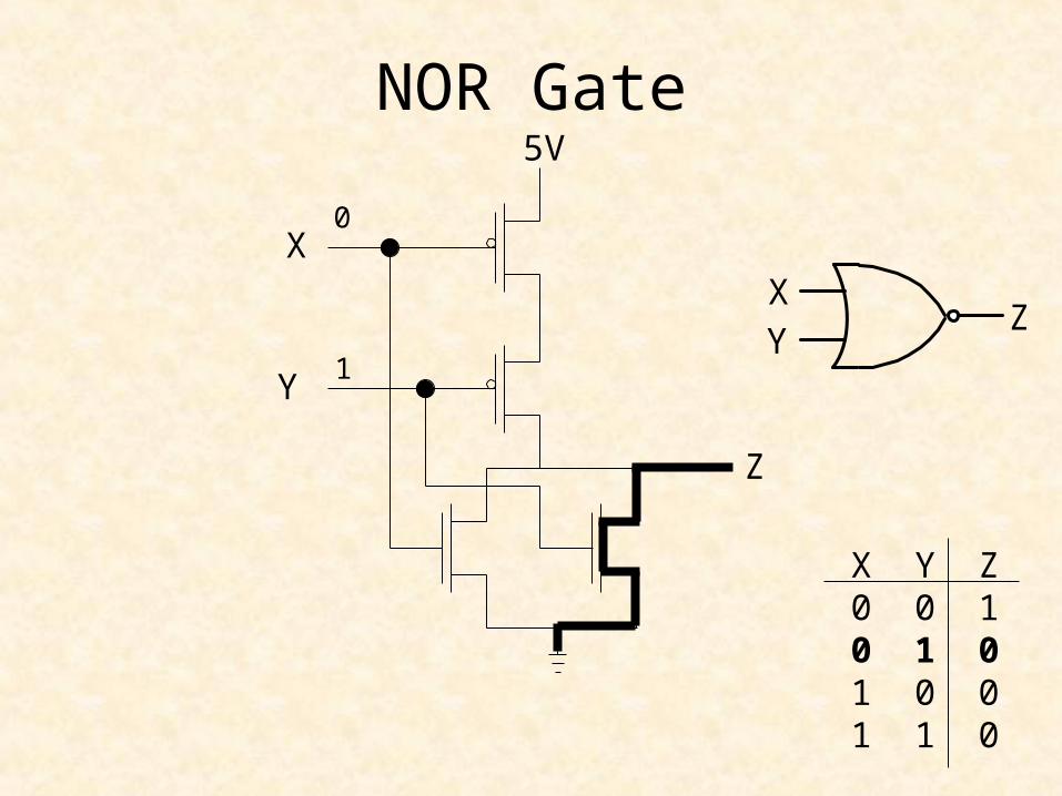
NOR Gate
X
Y
Z
5V
XY
Z
X Y Z0 0 10 1 01 0 01 1 0
0
0
NOR Gate
X
Y
Z
5V
XY
Z
X Y Z0 0 10 1 01 0 01 1 0
0
1
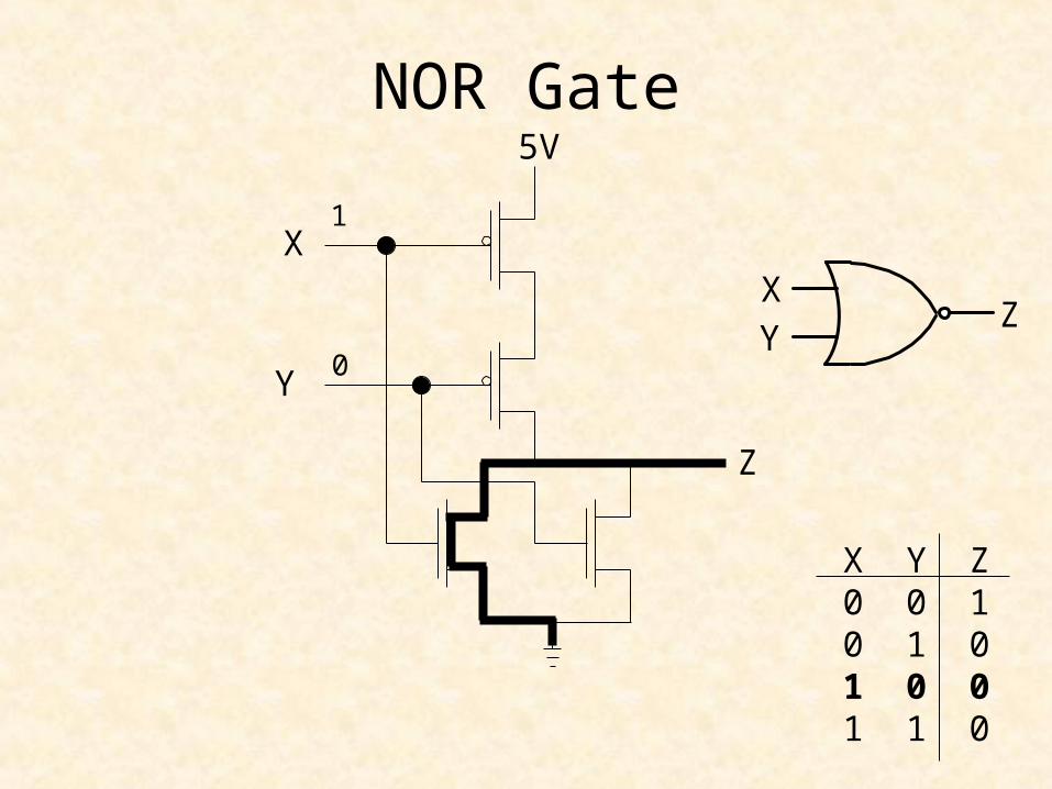
NOR Gate
X
Y
Z
5V
XY
Z
X Y Z0 0 10 1 01 0 01 1 0
1
0
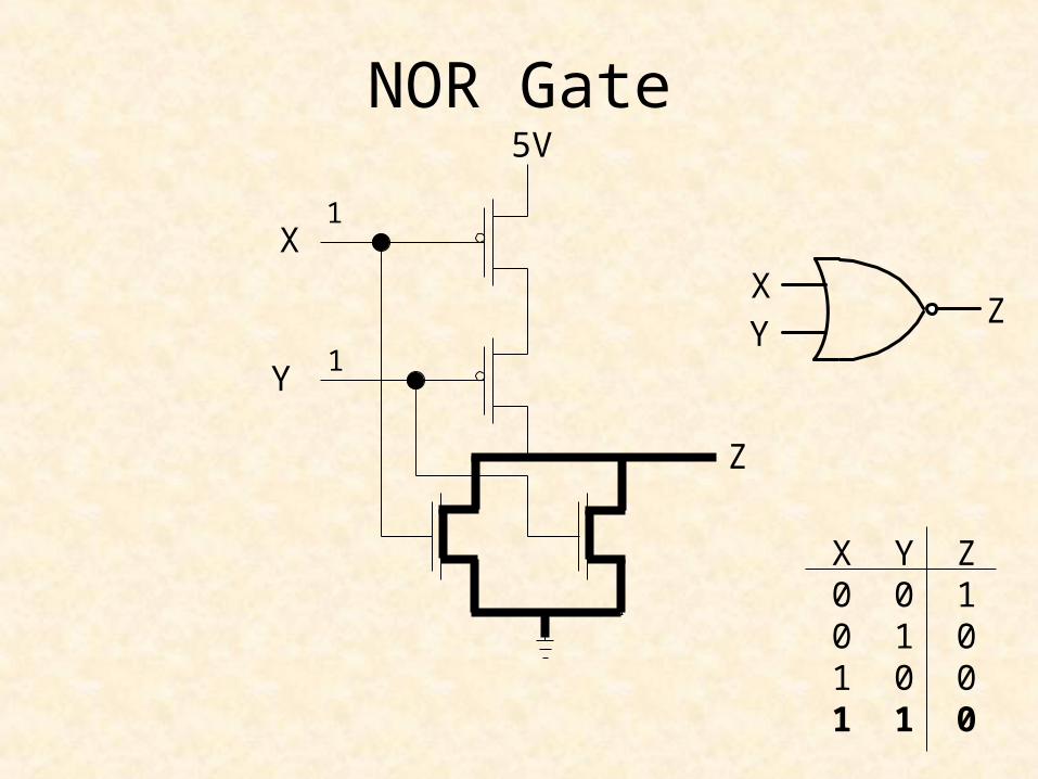
NOR Gate
X
Y
Z
5V
XY
Z
X Y Z0 0 10 1 01 0 01 1 0
1
1
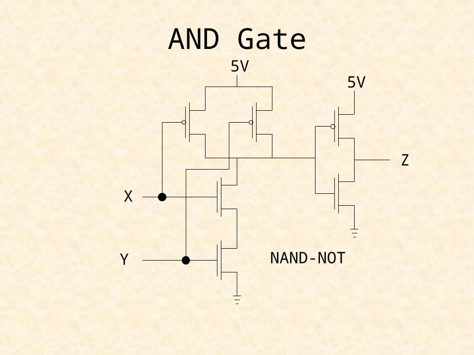
AND Gate
X
Y
5V
Z
5V
NAND-NOT

OR Gate
X
Y
5V
Z
5V
NOR-NOT
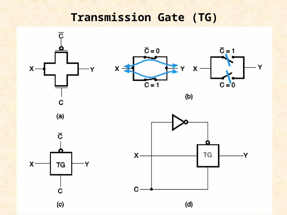
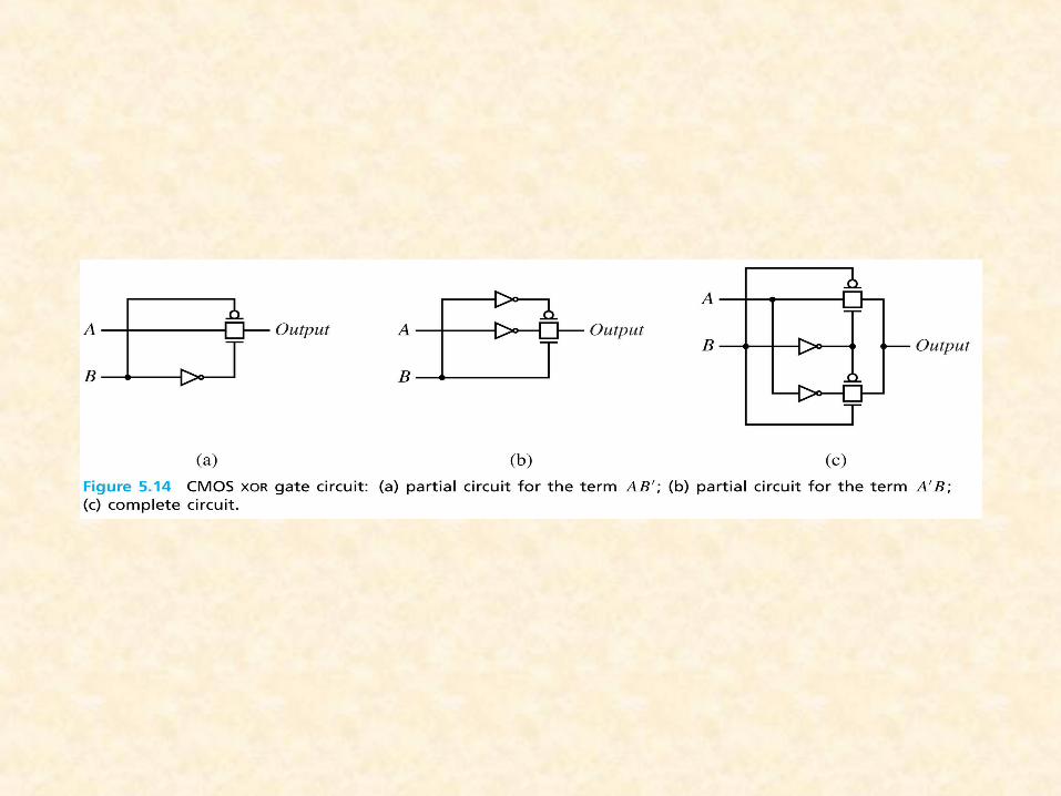
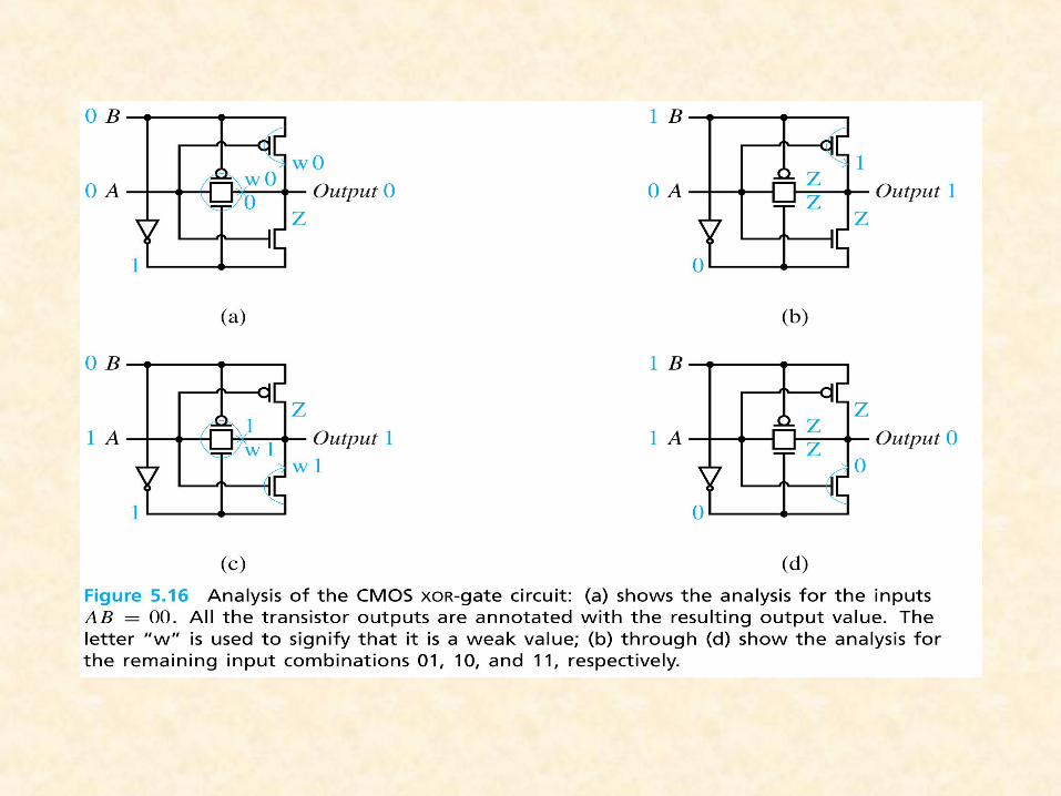
Transmission Gate (TG)
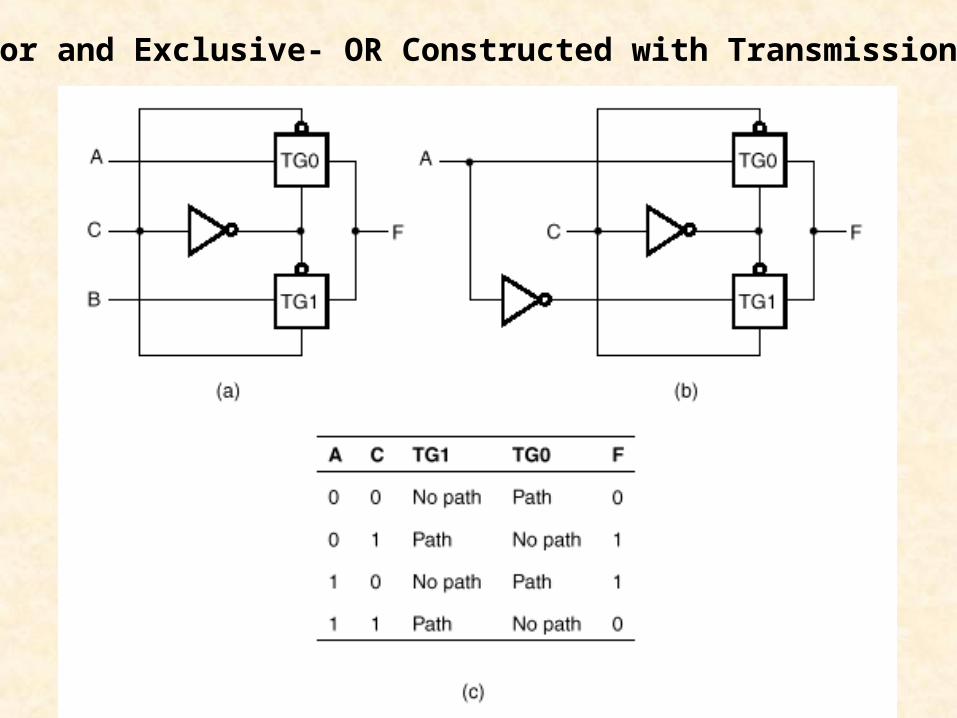
Selector and Exclusive- OR Constructed with Transmission Gates


Transistor-Transistor Logic(TTL)
• Developed in mid-1960s
• Large family (74xx) of chips from basic gates to arithmetic logic units
• Becoming obsolete with the development of programmable logic devices (PLDs)

TTL Chips
1 2 3 4 5 6 7
8 9 1011121314
1 2 3 4 5 6 7
8 9 1011121314
1 2 3 4 5 6 7
8 9 1011121314
7404 Hex Inverters
7408 Quad 2-Input AND Gates
7432 Quad 2-Input OR Gates
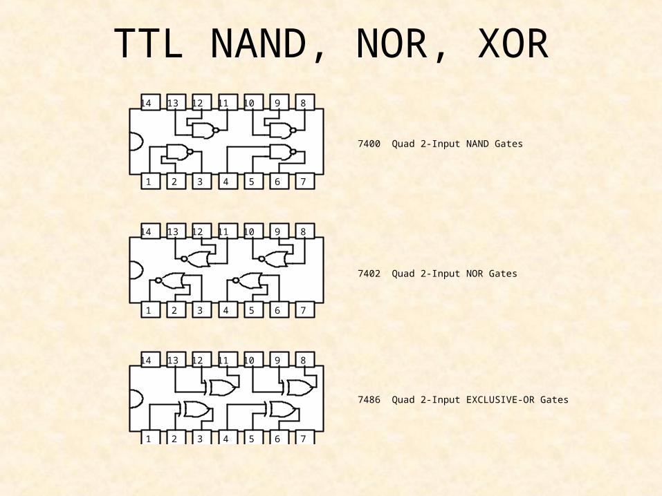
TTL NAND, NOR, XOR
1 2 3 4 5 6 7
8 9 1011121314
1 2 3 4 5 6 7
8 9 1011121314
1 2 3 4 5 6 7
8 9 1011121314
7400 Quad 2-Input NAND Gates
7402 Quad 2-Input NOR Gates
7486 Quad 2-Input EXCLUSIVE-OR Gates

TTL Multiple-input Gates
1 2 3 4 5 6 7
8 9 1011121314
1 2 3 4 5 6 7
8 9 1011121314
7421 Dual 4-Input AND Gates
7430 8-Input NAND Gate

Small-Scale Integrated (SSI) Circuits
• 1 to 10 gates
• NAND gate has 4 transistors

Medium-Scale Integrated (MSI) Circuits
• 10-100 gates
• Adders
• Comparators
• Multiplexers
• Decoders
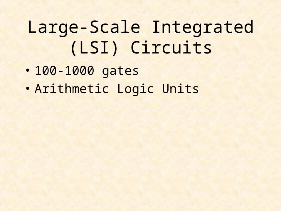
Large-Scale Integrated (LSI) Circuits
• 100-1000 gates
• Arithmetic Logic Units

Very-Large-Scale Integrated (VLSI) Circuits
• >1000 gates
• Microprocessors
• Programmable Logic Devices (PLDs)
• Complex Programmable Logic Devices (CPLDs)
• Field Programmable Gate Arrays (FPGAs)
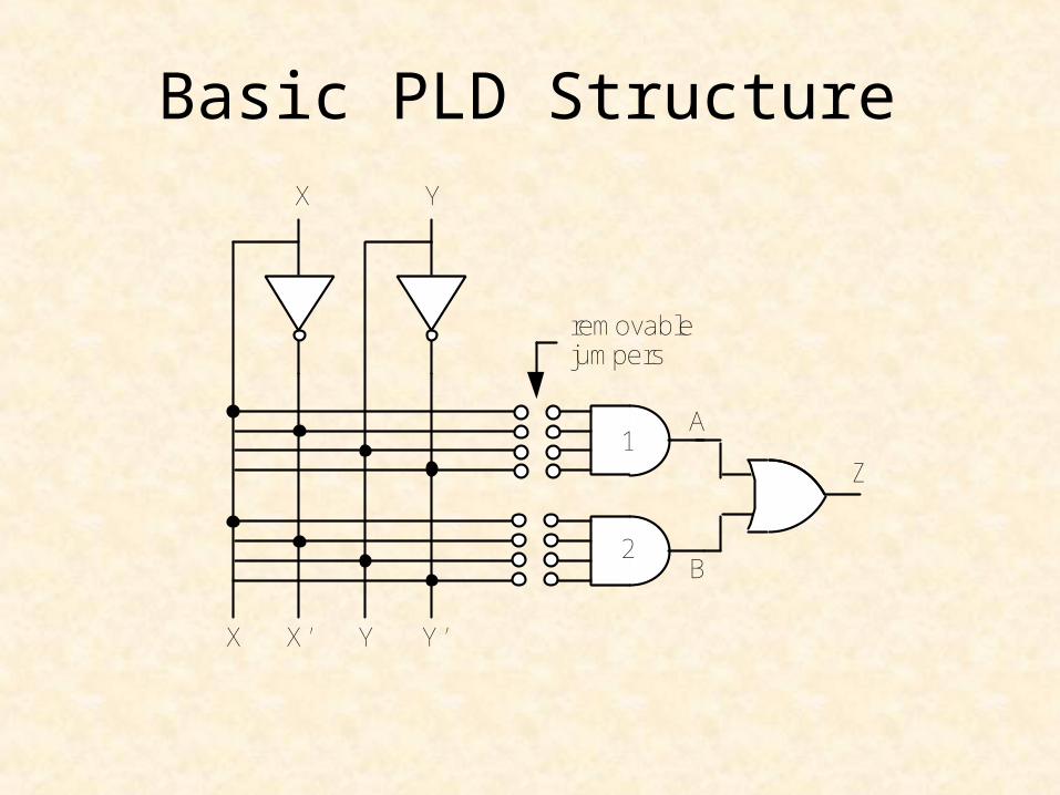
Basic PLD StructureX Y
X X’ Y Y’
A
B
1
2
Z
removablejumpers
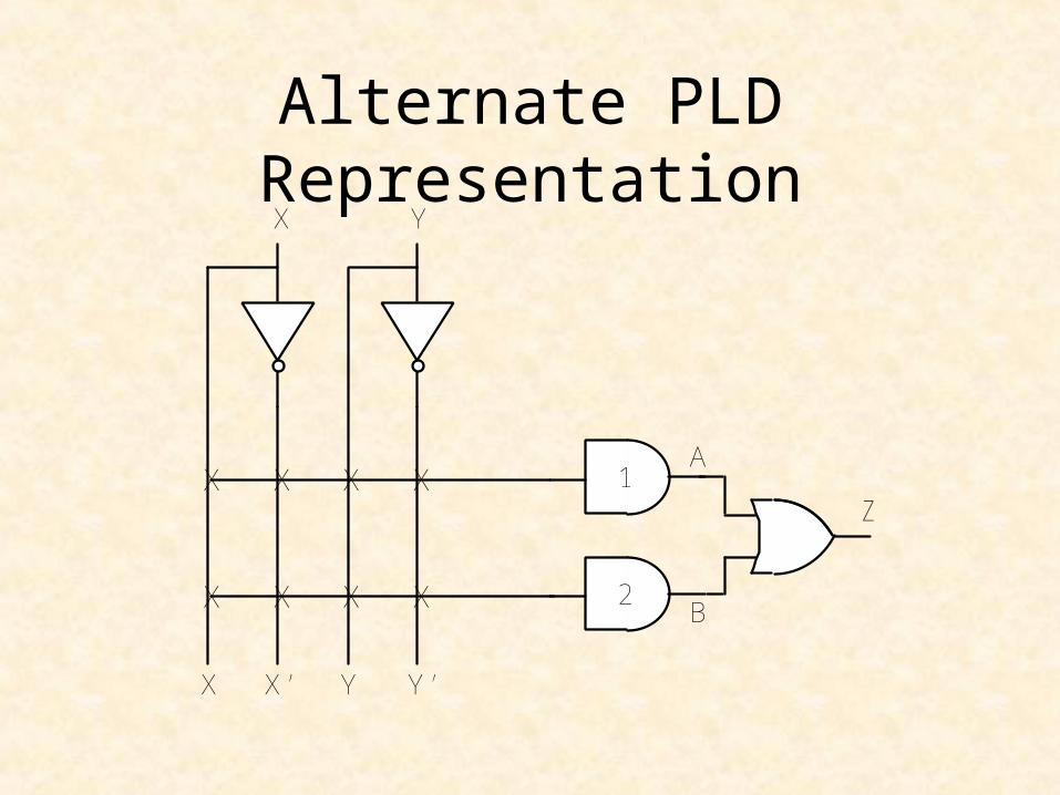
Alternate PLD RepresentationX Y
X X’ Y Y’
A
B
ZX X X X
X X X X
1
2

PLD Connections for XORX Y
X X’ Y Y’
A
B
Z = XY’ + X’Y
X X
X X
1
2

1975 – Signetics invents the FPLA
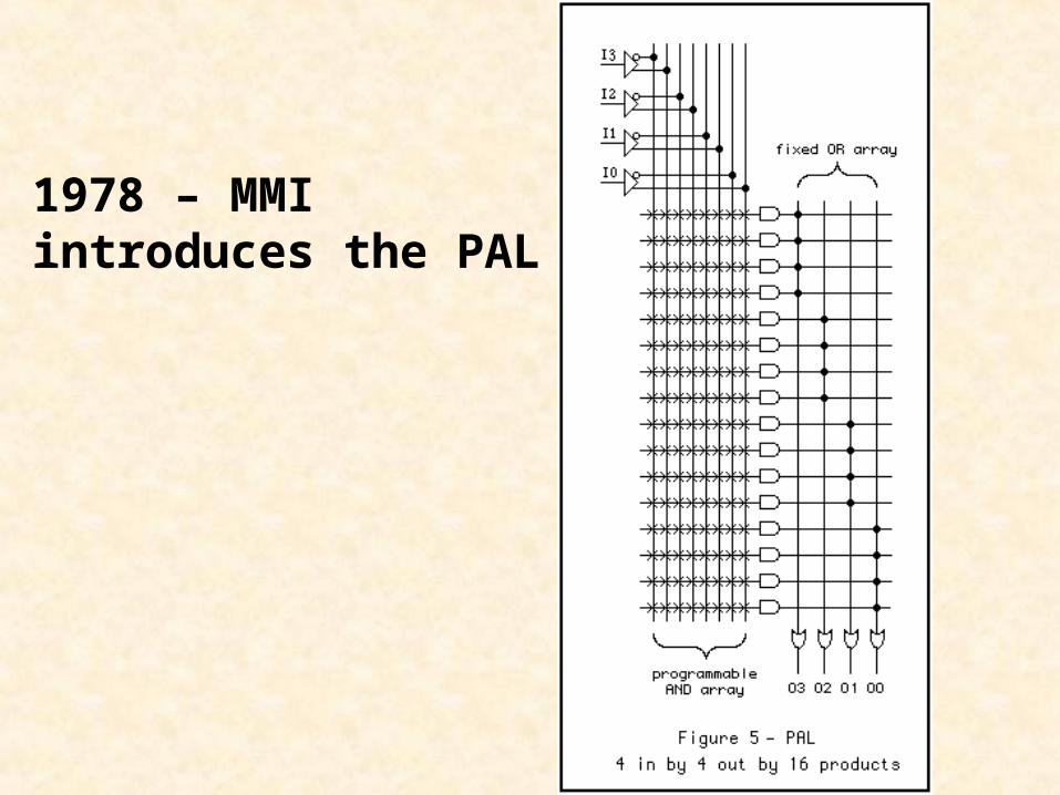
1978 – MMI introduces the PAL

1983 – AMD introduces the 22V10
1984 – Lattice introduces the GAL – an electrically erasable PAL

The GAL 16V8
1
2
3
4
5
6
7
9
10 11
12
8
19
20
17
18
15
16
13
14
GND
Vcc I/CLK I I/O
I I
I
I
I
I
I
I/OE
I/O
I/O
I/O
I/O
I/O
I/O
I/O
GAL 16V8

Structure of the GAL 16V8 PLDX X X X X X X X
X X X X X X X X
X X X X X X X X
X X X X X X X X
X X X X X X X X
X X X X X X X X
X X X X X X X X
X X X X X X X X
Pin 2
Pin 3
Pin 19
X
Y
Z
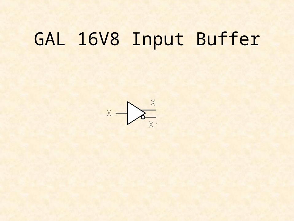
GAL 16V8 Input Buffer
XX
X’
Structure of the GAL 16V8 PLDX X X X X X X X
X X X X X X X X
X X X X X X X X
X X X X X X X X
X X X X X X X X
X X X X X X X X
X X X X X X X X
X X X X X X X X
Pin 2
Pin 3
Pin 19
X
Y
Z
GAL 16V8 Polarity Control
OE
X
A
B
C
X closed B = 0 C = A open B = 1 C = A'
Polarity
Pin

Structure of the GAL 16V8 PLDX X X X X X X X
X X X X X X X X
X X X X X X X X
X X X X X X X X
X X X X X X X X
X X X X X X X X
X X X X X X X X
X X X X X X X X
Pin 2
Pin 3
Pin 19
X
Y
Z
XC9500 CPLDs
• 5 volt in-system programmable (ISP) CPLDs
• 5 ns pin-to-pin• 36 to 288
macrocells (6400 gates)
• Industry’s best pin-locking architecture
• 10,000 program/erase cycles
• Complete IEEE 1149.1 JTAG capability
FunctionBlock 1
JTAGController
FunctionBlock 2
I/O
FunctionBlock 4
3
Global Tri-
States 2 or 4
FunctionBlock 3
I/O
In-SystemProgramming Controller
FastCONNECTSwitch Matrix
JTAG Port
3
I/O
I/O
Global Set/Reset
Global Clocks
I/OBlocks
1
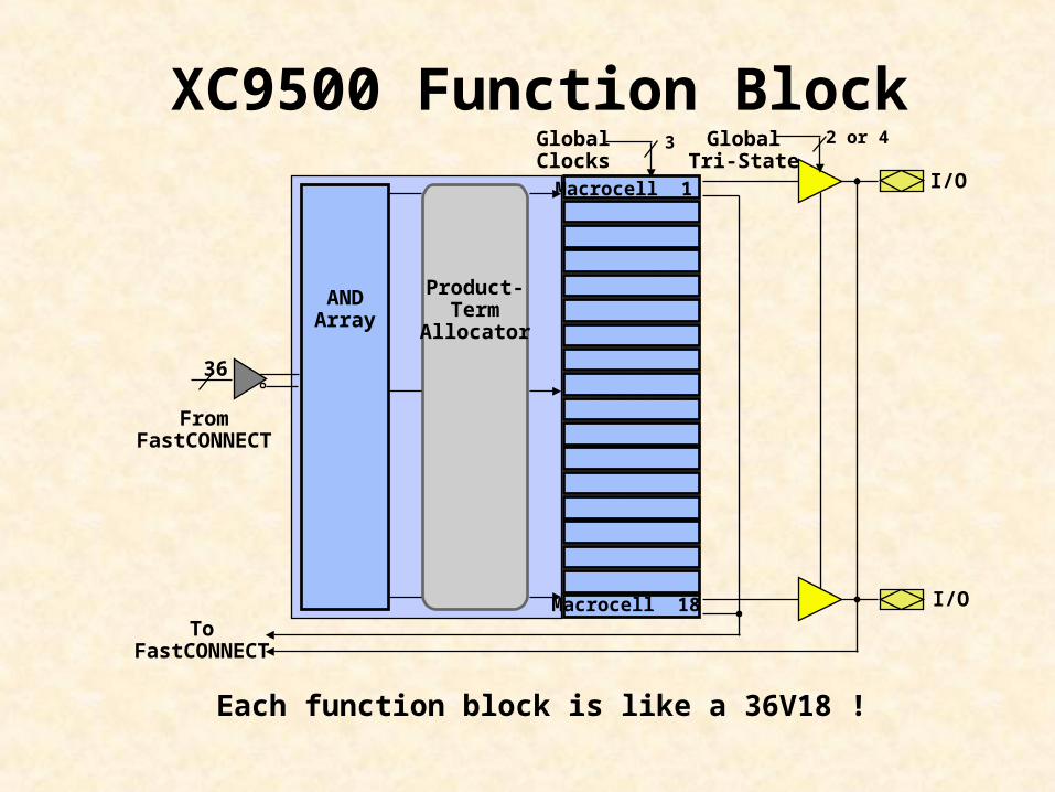
XC9500 Function Block
ToFastCONNECT
FromFastCONNECT
2 or 43 GlobalTri-State
GlobalClocks
I/O
I/O
36
Product-Term
Allocator
Macrocell 1
ANDArray
Macrocell 18
Each function block is like a 36V18 !

XC9500 Product Family
9536
Macrocells
Usable Gates
tPD (ns)
Registers
Max I/O
36 72 108 144 216
800 1600 2400 3200 4800
5 7.5 7.5 7.5 10
36 72 108 144 216
34 72 108 133 166
Packages VQ44PC44 PC44
PC84TQ100PQ100
PC84TQ100PQ100PQ160
PQ100PQ160
288
6400
10
288
192
HQ208BG352
PQ160HQ208BG352
9572 95108 95144 95216 95288

Xilinx 95108
• 6 function blocks– Each contains 18 macro cells– Each macro cell behaves like a GAL32V18
• AND-OR array for sum-of-products
• 32 inputs and 18 outputs
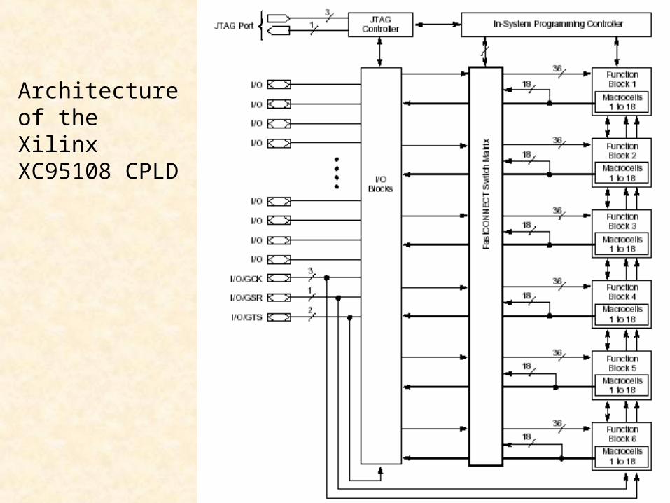
Architecture of the Xilinx XC95108 CPLD
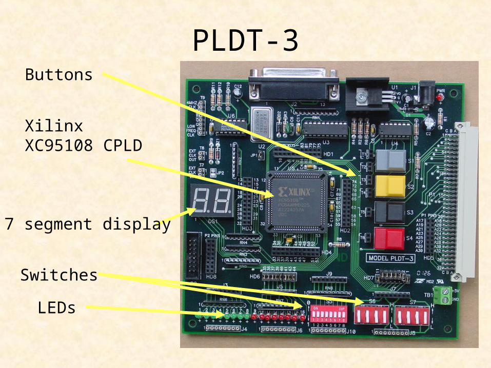
PLDT-3
XilinxXC95108 CPLD
7 segment display
Switches
LEDs
Buttons

PLDT-3
• 12 macro cells connected to I/O pins
• 4 pushbuttons
• 8 toggle switches
• 8 dip switches
• 16 LEDs
• 2 7-segment displays
• On-board clock signals (4 MHz and 1 Hz)

FPGAs
Field Programmable Gate Arrays
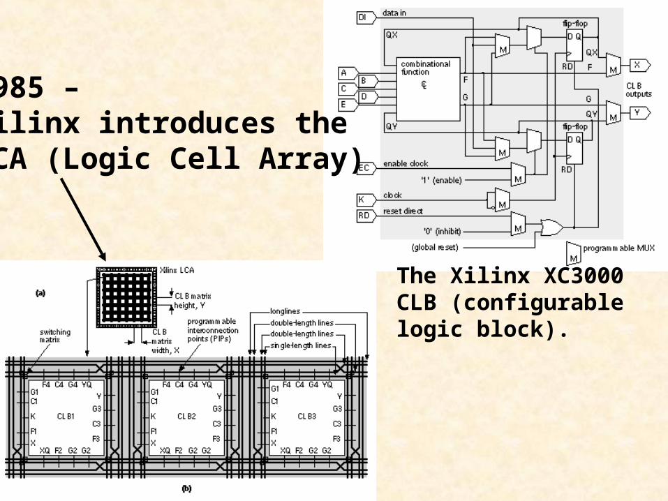
1985 – Xilinx introduces the LCA (Logic Cell Array)
The Xilinx XC3000 CLB (configurable logic block).
CLB
CLB
CLB
CLB
SwitchMatrix
ProgrammableInterconnect I/O Blocks (IOBs)
ConfigurableLogic Blocks (CLBs)
D Q
SlewRate
Control
PassivePull-Up,
Pull-Down
Delay
Vcc
OutputBuffer
InputBuffer
Q D
Pad
D QSD
RDEC
S/RControl
D QSD
RDEC
S/RControl
1
1
F'
G'
H'
DIN
F'
G'
H'
DIN
F'
G'
H'
H'
HFunc.Gen.
GFunc.Gen.
FFunc.Gen.
G4G3G2G1
F4F3F2F1
C4C1 C2 C3
K
Y
X
H1 DIN S/R EC
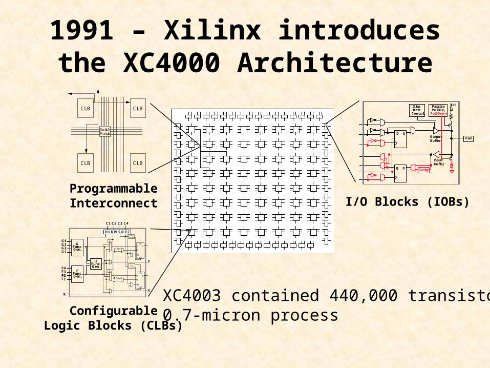
1991 – Xilinx introduces the XC4000 Architecture
XC4003 contained 440,000 transistors0.7-micron process

XC4000E/X Configurable Logic Blocks
D QSD
RDEC
S/RControl
D QSD
RDEC
S/RControl
1
1
F'
G'
H'
DIN
F'
G'
H'
DIN
F'
G'
H'
H'
HFunc.Gen.
GFunc.Gen.
FFunc.Gen.
G4G3G2G1
F4F3F2F1
C4C1 C2 C3
K
YQ
Y
XQ
X
H1 DIN S/R EC
• 2 Four-input function generators (Look Up Tables)- 16x1 RAM or Logic function
• 2 Registers- Each can be configured as Flip Flop or Latch- Independent clock polarity- Synchronous and asynchronous Set/Reset

Look Up Tables
Capacity is limited by number of inputs, not complexity
Choose to use each function generator as 4 input logic (LUT) or as high speed sync.dual port RAM
• Combinatorial Logic is stored in 16x1 SRAM Look Up Tables (LUTs) in a CLB
• Example:
A B C D Z
0 0 0 0 00 0 0 1 00 0 1 0 00 0 1 1 10 1 0 0 10 1 0 1 1 . . .1 1 0 0 01 1 0 1 01 1 1 0 01 1 1 1 1
Look Up Table
Combinatorial Logic
AB
CD
Z
4-bit address
GFunc.Gen.
G4G3G2G1
WE
2(2 )4
= 64K !

What’s Really In that Chip?
CLB(Red)
Switch Matrix
Long Lines(Purple)
Direct Interconnect (Green)
Routed Wires (Blue)
Programmable Interconnect Points, PIPs (White)

1998 – Xilinx introduces the Virtex®™ FPGA family
0.25-micron process

2003 – Xilinx introduces the Spartan®™-3 family of products
Very low cost
World’s first90 nm FPGA
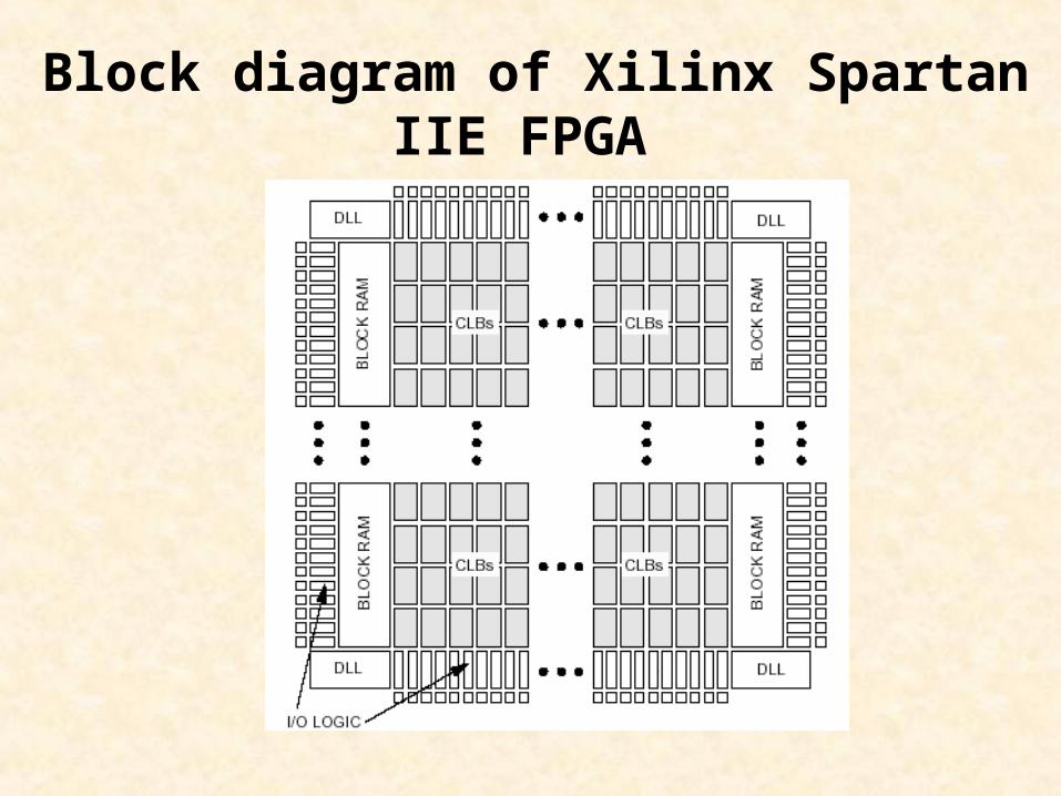
Block diagram of Xilinx Spartan IIE FPGA
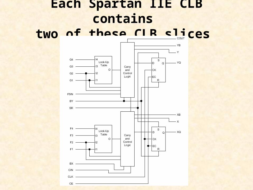
Each Spartan IIE CLB contains two of these CLB slices

Block diagram of Xilinx Spartan-3 FPGA
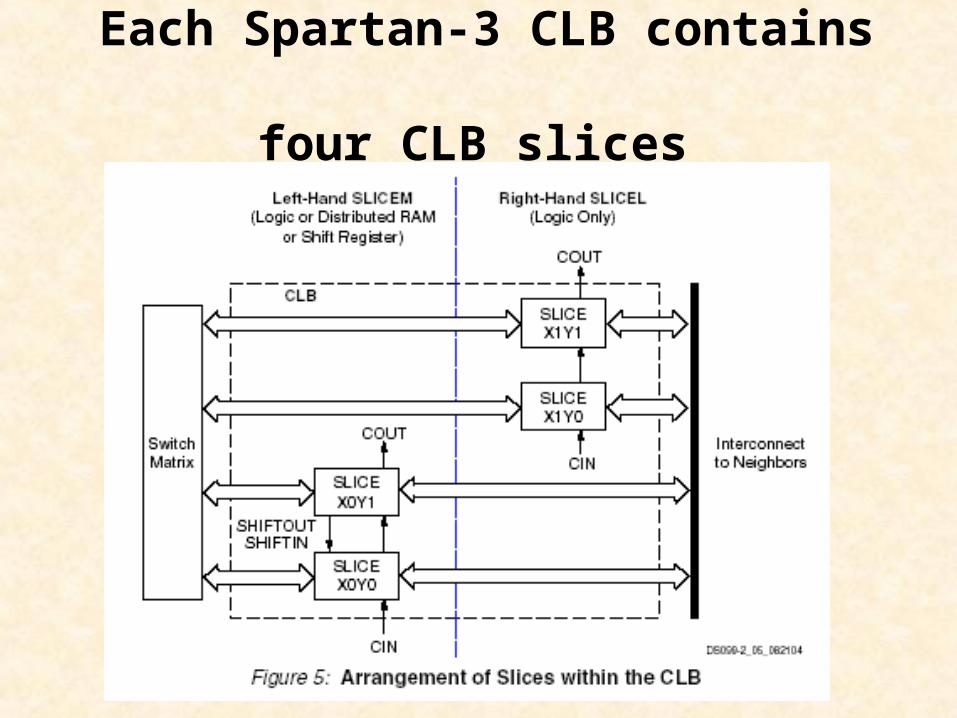
Each Spartan-3 CLB contains four CLB slices

Spartan 3 Board

CPLDs vs. FPGAs

Moore's Law(Doubling every 2 years)
0.001
0.01
0.1
1
10
100
1000
10000
1974 1976 1978 1980 1982 1984 1986 1988 1990 1992 1994 1996 1998 2000 2002 2004 2006 2008 2010
Year
Tra
nsi
sto
rs (
in m
illio
ns
)
8080
286
486 Pentium
Pentium II
Pentium 4
64K
1M
4M
16M
Memory
Microprocessor
x
Xilinx will release the world’s first one-billion transistor device this year