IMPLEMENTATION OF PWM BASED FIRING SCHEME FOR MULTILEVEL ...

Czech Technical University in Prague
Faculty of Electrical Engineering
Department of Control Engineering
DIPLOMA THESIS
Implementation of a new PWM approachfor class-D digital audio amplifier
Author: Bc. Nguyen Hong Quang
Supervisor: Ing. Petr Kujan, Ph.D
Opponent: Ing. Tran Duy Khanh
In Prague December 12, 2010


Declaration
I declare that I have created my Diploma Thesis on my own and I have used only
literture cited in the included reference list.
In Prague,
signature
i

Acknowledgements
First and foremost, I would like to express my deep gratitude to Ing. Petr Kujan, Ph.D,
my supervisor, for carefull leadingand usefull comments in creating this thesis. Discussing
with him is always an interesting experience by which I has broadened my knowledge to
new horizons and realized how prudent a researcher should be. Without his helps, it would
have been very difficult for me in creating of this work. Though being late connected
to my work, he still gave me valuable suggestions for the improvements. His regularly
encouragement and responsibility always raised me up in the progress of doing this work.
This thesis could not have been completed without practical information and materi-
als. Without the opportunity to collect data material by myself, I had to rely completely
on the help of Ing. Tran Duy Khanh. It is hard for me to describe my sincere apprecia-
tion to his efforts to help me despite the difficulties arose during the process, but with his
support and helpful advices, that helped me to develop the understading of the problem.
Last but not least, my deepest gratitude goes to my beloved parents, my brother
and my girlfriend who made it always possible to fulfill my study and non-study related
desires and who are always by my side, encourage me, accept my mistakes, and make me
feel proud whenever I have tried my best.
Then, many thanks to to all friends who helped and gave a hand, without their
support it wouldn’t have been possible for me to finish this work.
ii

Abstract
In this diploma thesis I would like to present a new approach to develop the digital class-D
audio amplifier. Then I will describe one of the alternate implemetations for generating
the optimal pulse width modulation (PWM) of odd bi-level waveform.
The optimal PWM algorithm is used to solve problem of generating the PWM output
switching waveform when the input are well-known frequency spectrums. The main task
of this problem is to determine switching times, where the PWM signal changes its state.
We have also discovered that with using this algorithm we can determine all n numbers
of switching times in O(n log2 n) times.
Further, the algorithm has been implemented off-line in programming language C with
using ARM GNU software/tools, where the coding algorithm is performed by software
routines that wrote to a file switching times instants. Input data are then fed to a very
simple hardware - a microcontroller that generates a PWM-like output signal to directly
drive a high-efficiency switching audio amplifier. The final result of the implementation
shows the hardware architecture is used to implement the algorithm, it requires a hight
frequency speed to generate precisely PWM output conresponding to switching times.
iii

Contents
List of Figures vii
List of Tables ix
1 Introduction 1
1.1 Objectives of the Thesis . . . . . . . . . . . . . . . . . . . . . . . . . . . 2
1.2 Methods . . . . . . . . . . . . . . . . . . . . . . . . . . . . . . . . . . . . 2
1.3 Outline of the Thesis . . . . . . . . . . . . . . . . . . . . . . . . . . . . . 3
2 Requirements analysis and system architecture 4
2.1 Overview of digital class-D audio amplifiers . . . . . . . . . . . . . . . . . 4
2.1.1 History . . . . . . . . . . . . . . . . . . . . . . . . . . . . . . . . . 4
2.1.2 Basic principles . . . . . . . . . . . . . . . . . . . . . . . . . . . . 6
2.2 New strategy to implement the digital class-D audio amplifier . . . . . . 8
2.2.1 Frequency spectrum of odd signal . . . . . . . . . . . . . . . . . . 10
2.2.1.1 Fast Fourier Transform of odd signal . . . . . . . . . . . 10
2.2.1.2 Efficient Fast Fourier Transform (FFT) algorithm . . . . 13
2.2.2 Optimal PWM modulation problem of odd bi-level waveform . . . 14
2.2.2.1 Algorithm of odd bi-level PWM waveform . . . . . . . . 17
2.3 System architecture . . . . . . . . . . . . . . . . . . . . . . . . . . . . . . 20
2.3.1 Architectural design . . . . . . . . . . . . . . . . . . . . . . . . . 20
2.3.1.1 Hardware components . . . . . . . . . . . . . . . . . . . 20
2.3.1.2 Software components . . . . . . . . . . . . . . . . . . . . 21
3 Hardware Support 23
3.1 Hardware componnents . . . . . . . . . . . . . . . . . . . . . . . . . . . . 23
3.1.1 AT91SAM9G20 processor . . . . . . . . . . . . . . . . . . . . . . 23
3.1.2 Embedded modules . . . . . . . . . . . . . . . . . . . . . . . . . . 26
iv

3.1.2.1 The module OC8-S . . . . . . . . . . . . . . . . . . . . . 26
3.1.2.2 The OC8-H header board . . . . . . . . . . . . . . . . . 28
3.2 Software issues for OC8-S . . . . . . . . . . . . . . . . . . . . . . . . . . 28
4 Starting with an embedded Linux 30
4.1 Overview . . . . . . . . . . . . . . . . . . . . . . . . . . . . . . . . . . . . 30
4.2 Configuring the software environment . . . . . . . . . . . . . . . . . . . . 32
4.2.1 Hosting Target Boards . . . . . . . . . . . . . . . . . . . . . . . . 33
4.3 The GNU Toolchain . . . . . . . . . . . . . . . . . . . . . . . . . . . . . 35
4.4 Bootloader . . . . . . . . . . . . . . . . . . . . . . . . . . . . . . . . . . . 37
4.4.1 A Universal Bootloader: Das U-Boot . . . . . . . . . . . . . . . . 38
4.4.2 Building U-boot . . . . . . . . . . . . . . . . . . . . . . . . . . . . 39
4.4.3 Downloading the U-Boot onto OC8-S . . . . . . . . . . . . . . . . 40
4.4.4 Important routines . . . . . . . . . . . . . . . . . . . . . . . . . . 41
4.5 Linux distribution . . . . . . . . . . . . . . . . . . . . . . . . . . . . . . . 44
4.5.1 Getting an embedded Linux . . . . . . . . . . . . . . . . . . . . . 44
4.5.2 Adding new drivers and application . . . . . . . . . . . . . . . . . 45
5 Software 48
5.1 USART device driver . . . . . . . . . . . . . . . . . . . . . . . . . . . . . 48
5.1.1 Overview . . . . . . . . . . . . . . . . . . . . . . . . . . . . . . . 48
5.1.2 Implementation of USART driver . . . . . . . . . . . . . . . . . . 49
5.2 Fast Fourier Transform . . . . . . . . . . . . . . . . . . . . . . . . . . . . 57
5.3 The optimal PWM . . . . . . . . . . . . . . . . . . . . . . . . . . . . . . 60
5.4 Compiling driver and aplication . . . . . . . . . . . . . . . . . . . . . . . 62
6 Testing and final work 63
6.1 Software testing . . . . . . . . . . . . . . . . . . . . . . . . . . . . . . . . 63
6.1.1 The optimal PWM algorithm . . . . . . . . . . . . . . . . . . . . 63
6.2 Embedded PWM generator . . . . . . . . . . . . . . . . . . . . . . . . . 67
6.3 Frequent error scenarios . . . . . . . . . . . . . . . . . . . . . . . . . . . 71
6.4 Final work . . . . . . . . . . . . . . . . . . . . . . . . . . . . . . . . . . . 71
7 Conclusion 73
v

A Algorithms/Mathematical Background I
A.1 QR decomposition . . . . . . . . . . . . . . . . . . . . . . . . . . . . . . I
A.2 A pseudocode algorithm for finding real and complex roots of real polyno-
mials with multiple roots . . . . . . . . . . . . . . . . . . . . . . . . . . . II
B Content of the Attached CD III
vi

List of Figures
1.1 General scheme for the digital class-D audio amplifier. . . . . . . . . . . . 2
2.1 The classification of audio amplifiers class-D. . . . . . . . . . . . . . . . . 5
2.2 A basic audio amplifier class-D with PWM comparator, FET output stage,
and second-order LC output filter . . . . . . . . . . . . . . . . . . . . . . 6
2.3 The PWM process as performed by a differential comparator . . . . . . . 7
2.4 Scheme of h-bridge for audio amplifiers class-D . . . . . . . . . . . . . . . 7
2.5 Familiar versions of filters for h-bridge output . . . . . . . . . . . . . . . 8
2.6 Block diagram of the proposed class-D audio amplifier . . . . . . . . . . . 8
2.7 Main tasks of the block Audio signal/Optimal PWM . . . . . . . . . . . . 9
2.8 Block diagram of the digital class-D audio amplifier implemented by the
optimal PWM algorithm . . . . . . . . . . . . . . . . . . . . . . . . . . . 9
2.9 The principle of audio amplifier class-D using the optimal PWM algorithm
of odd signal. . . . . . . . . . . . . . . . . . . . . . . . . . . . . . . . . . 10
2.10 The tree of input vectors to the iterative calls of the FFT procedure. . . 13
2.11 (a) Frequency spectrum of a separated base-band signal. The base-band
can be recovered by an LPF. (b) Principal scheme for optimal PWM prob-
lem. . . . . . . . . . . . . . . . . . . . . . . . . . . . . . . . . . . . . . . 15
2.12 Odd bi-level PWM waveform. . . . . . . . . . . . . . . . . . . . . . . . . 16
3.1 AT91SAM9G20 Block Diagram . . . . . . . . . . . . . . . . . . . . . . . 25
3.2 The embedded processor module Linux systems OC8-S . . . . . . . . . . 26
3.3 Hardware architecture of the module OC8-S . . . . . . . . . . . . . . . . 27
3.4 The OC8-H header board . . . . . . . . . . . . . . . . . . . . . . . . . . 28
4.1 Cross-development setup . . . . . . . . . . . . . . . . . . . . . . . . . . . 33
5.1 The block diagram of USART . . . . . . . . . . . . . . . . . . . . . . . . 49
5.2 Principle of gpio pwm write() . . . . . . . . . . . . . . . . . . . . . . . . . 54
vii

5.3 A circular buffer . . . . . . . . . . . . . . . . . . . . . . . . . . . . . . . . 54
5.4 Bit reversal process in FFT . . . . . . . . . . . . . . . . . . . . . . . . . 58
6.1 Odd bi-level PWM waveform for n = 20 . . . . . . . . . . . . . . . . . . 65
6.2 Spectrums of odd bi-level PWM waveform for n = 20 . . . . . . . . . . . 65
6.3 PWM output signal for n = 5 . . . . . . . . . . . . . . . . . . . . . . . . 67
6.4 Simulated odd bi-level PWM waveform for n = 5 . . . . . . . . . . . . . 67
6.5 The first period of the real PWM output signal for n = 5 . . . . . . . . . 68
6.6 The measured and computed PWM output signal fo n = 5 . . . . . . . . 68
6.7 PWM output signal for n = 4 . . . . . . . . . . . . . . . . . . . . . . . . 69
6.8 Simulated odd bi-level PWM waveform for n = 4 . . . . . . . . . . . . . 69
6.9 The first period of the real PWM output signal for n = 4 . . . . . . . . . 70
6.10 The real and computed PWM output signal for n = 4 . . . . . . . . . . . 70
7.1 The prototype of the digital class-D audio amplifier. . . . . . . . . . . . . 74
viii

List of Tables
4.1 Display all serial ports . . . . . . . . . . . . . . . . . . . . . . . . . . . . 33
4.2 Detailed info about setial devices on the USB ports . . . . . . . . . . . . 34
4.3 Minicom terminal . . . . . . . . . . . . . . . . . . . . . . . . . . . . . . . 34
4.4 TFTP Configuration . . . . . . . . . . . . . . . . . . . . . . . . . . . . . 35
4.5 NFS Server Configuration . . . . . . . . . . . . . . . . . . . . . . . . . . 35
4.6 Unpacking toolchain . . . . . . . . . . . . . . . . . . . . . . . . . . . . . 37
4.7 Configuration address for CodeSoucery in workstation. . . . . . . . . . . 37
4.8 Create default configuration OC8-S . . . . . . . . . . . . . . . . . . . . . 39
4.9 Configuration U-Boot. . . . . . . . . . . . . . . . . . . . . . . . . . . . . 40
4.10 Cross-compiling. . . . . . . . . . . . . . . . . . . . . . . . . . . . . . . . . 40
4.11 Das U-Boot . . . . . . . . . . . . . . . . . . . . . . . . . . . . . . . . . . 41
4.12 U-Boot’s network settings . . . . . . . . . . . . . . . . . . . . . . . . . . 41
4.13 U-Boot’s network settings . . . . . . . . . . . . . . . . . . . . . . . . . . 42
4.14 Erasing the flash memory . . . . . . . . . . . . . . . . . . . . . . . . . . 42
4.15 Writting uImage to the Flash memory . . . . . . . . . . . . . . . . . . . 42
4.16 Downloading the root file system . . . . . . . . . . . . . . . . . . . . . . 43
4.17 Writting the root file system to the Flash memory . . . . . . . . . . . . . 43
4.18 Reading of the uImage to the RAM . . . . . . . . . . . . . . . . . . . . . 43
4.19 The boot parameter . . . . . . . . . . . . . . . . . . . . . . . . . . . . . 43
4.20 Boot uImage . . . . . . . . . . . . . . . . . . . . . . . . . . . . . . . . . . 44
4.21 Getting the kernel source . . . . . . . . . . . . . . . . . . . . . . . . . . . 45
4.22 Configuration of the Linux kernel . . . . . . . . . . . . . . . . . . . . . . 45
4.23 Creating the Linux kernel . . . . . . . . . . . . . . . . . . . . . . . . . . 45
4.24 Set PATH environtmnet for compiling . . . . . . . . . . . . . . . . . . . . 46
4.25 Creating the Linux kernel . . . . . . . . . . . . . . . . . . . . . . . . . . 46
4.26 Loading the device driver to kernel . . . . . . . . . . . . . . . . . . . . . 46
4.27 Creating a user application . . . . . . . . . . . . . . . . . . . . . . . . . . 47
ix

4.28 Loading application onto OC8-S . . . . . . . . . . . . . . . . . . . . . . . 47
5.1 Define module parameters . . . . . . . . . . . . . . . . . . . . . . . . . . 50
5.2 Define pinout . . . . . . . . . . . . . . . . . . . . . . . . . . . . . . . . . 50
5.3 Peripheral initialization . . . . . . . . . . . . . . . . . . . . . . . . . . . . 51
5.4 File operations structure . . . . . . . . . . . . . . . . . . . . . . . . . . . 51
5.5 File structure . . . . . . . . . . . . . . . . . . . . . . . . . . . . . . . . . 52
5.6 Using mutex . . . . . . . . . . . . . . . . . . . . . . . . . . . . . . . . . . 53
5.7 Interrupt handler . . . . . . . . . . . . . . . . . . . . . . . . . . . . . . . 56
5.8 Bit-reversed function . . . . . . . . . . . . . . . . . . . . . . . . . . . . . 58
5.9 Fast Fourier Transform . . . . . . . . . . . . . . . . . . . . . . . . . . . . 59
6.1 The partial results for case n = 20, nC = 5, nE = 15, A = 10, T = 0.01 and
(bf1 , bf2 , bf3, bf4 , bf5) = (4,−5, 3, 1,−2) . . . . . . . . . . . . . . . . . . . . 64
6.2 The partial results for case n = 5, nC = 1, nE = 4, A = 15, T = 0.0002 and
(bf1) = (15) . . . . . . . . . . . . . . . . . . . . . . . . . . . . . . . . . . 66
6.3 Execute optimalpwm . . . . . . . . . . . . . . . . . . . . . . . . . . . . . 67
6.4 The partial results for case n = 4, nC = 1, nE = 3, A = 6, T = 0.001 and
(bf1) = (3). . . . . . . . . . . . . . . . . . . . . . . . . . . . . . . . . . . . 69
6.5 Show the status of modules in the Linux Kernel . . . . . . . . . . . . . . 71
x

Chapter 1
Introduction
In practice, audio amplifiers class-D use pulse width modulation (PWM) as the preferred
modulation technique to generate the output switching waveform. A controller converts
analog or digital audio to a PWM signal then it is amplified by the maturing of metal-
oxidesemiconductor field-effect transistors(MOSFETs). In fact, PWM presents a signal
into a few discrete levels, with the information represented in pulse duty ratios. The
digital audio signal is perfect for making PWM signal when all digital audio has a finite
resolution. This resolution can be quickly translated into a set pulse width, effectively
eliminating a A/D then D/A conversion which can cause errors in the signal due to re-
sampling. These varying pulse widths can be used to drive the h-bridge circuits present
in the class-D amplifiers to the correct positive or negative state for its given length of
time. Of course we have to account for switching losses and discontinuous states, but
audio amlifiers class-D with a good control algorithm can easily reach 90% efficiency.
Various simplified works have been used to implement a digital audio amplifier that
can be divided into three groups: the first one is the derivation of digital PWM techniques,
the second one is the design of digital controller for audio amplifier class-D and the last one
is the design of digital audio interface. A principle of interpolation methods for sampled
data conversion and noise shaping techniques for improving the spectral distortion are
cause why audio amplifiers class-D have a high reliability. Audio amplifiers class-D use
different kind of h-bridge or full-bridge topologies to reach the hight-efficency goal [1].
1

CHAPTER 1. INTRODUCTION 2
1.1 Objectives of the Thesis
The primary objective of this thesis is to propose a new strategy to implement a digital
class-D audio amplifier. In this diploma thesis, the optimal PWM algorithm of odd bi-
level waveform is used to implement. We will try determine switching times of PWM
output signal when the input are well-known frequency spectrums.
The secondary objective is to propose, develop and implement the algorithm of the
optimal PWM odd bi-level waveform in programming language C for an embedded mod-
ule with using ARM GNU software/tools. Furthermore, the validity of the implemented
algorithm will have to be verified by a selected hardware prototype with platform ARM9.
1.2 Methods
Objectives of this thesis are accomplished via the algorithm of the optimal PWM odd
bi-level waveform from detailed background study of the topic and to develop a general
scheme like Figure 1.1, that uses this algorithm to implement with a prototype of the
digital class-D audio amplifier. To do this, it requires a PC to pass values from well-
known frequency spectrums to the embedded module OC8-S based on the ARM9 ATMEL
AT91SAM9G20, in that is already implemeted the algorithm of optimal PWM odd bi-
level waveform. This module will take these values into a buffer and then release these
bits of information at sampling rate and it will pass the PWM control signal to the h-
bridge power converter. The h-bridge output will be filtered and delivered to a speaker
load. Rather a simple microcontroller will be used, because it is a simple and universal
hardware with a building embedded linux system for development.
Figure 1.1: General scheme for the digital class-D audio amplifier.

CHAPTER 1. INTRODUCTION 3
1.3 Outline of the Thesis
This section will give an overview about the work that was done. The chapters this
document is divided into correspond to phases of development.
• Chapter 1 − Introduction presents the studied topic and proposed goals of the
thesis. It gives insight to a implementation of the optimal PWM of odd bi-level
waveform.
• Chapter 2 − Requirements analysis and system architecture contains a de-
tailed requirements analysis and system architecture for the digital class-D audio
amplifiers. Basic inputs and outputs are determined and a list of required hardware
and software components is made.
• Chapter 3 − Hardware Support presents the embedded hardware Linux sup-
ports to develop the digital class-D audio amplifiers. The hardware components are
introduced and configured. The selected hardware builds upon a ARM9 processor
from ATMEL. Chapter ends with software issues for OC8-S.
• Chapter 4 − Starting with the embedded Linux introduces the embedded
Linux operating system for the ARM9 processor. In this chapter, the exercised of
configuring the software environment will be described and components that are
required for a complete embedded Linux operating system will be specified.
• Chapter 5 − Software is the main chapter of this document because it describes
the software development phase. Device driver is implemented first: For US-
ART(Universal Synchronous Asynchronous Receiver Transceiver) one has to be
implemented for an embedded Linux kernel. Thereafter, two user space applica-
tions are developed: The Fast Fourier Transform and the optimal PWM algorithm.
• Chapter 6 − Testing and final work deals with testing and final work. Accurate
testing is conducted with the main application. Finally, the work is completed by
deploying the software onto the target.
• Chapter 7 − Conclusion summarizes goals and obtained results of the thesis.
Problems are pointed out and a list of imaginable future enhancements of the digital
class-D audio amplifiers is presented

Chapter 2
Requirements analysis and system
architecture
This chapter presents various sections about the planning phase of a prototype audio
amplifier class-D. The requirements elicitation process starts with basic principles of
audio amplifiers class-D where a general idea about the capabilities of the system is
found. Afterwards, a new strategy to implement a prototype audio amplifier class-D is
described. Furthermore, the hardware/software component analysis is detailed described
in section system architecture .
2.1 Overview of digital class-D audio amplifiers
2.1.1 History
The task of a power audio amplifier is to reproduce input audio signals at sound produc-
ing output elements, with desired volume and power levels faithfully, efficiently, and at
low distortion. Audio frequencies range from about 20 Hz to 20 kHz, so the amplifier
must have good frequency response over this range (less when driving a band-limited
speaker, such as a woofer or a tweeter). Power capabilities vary widely depending on the
application, from milliwatts in headphones, to a few watts in TV or PC audio, to tens of
watts for ”mini” home stereos and automotive audio, to hundreds of watts and beyond
for more powerful home and commercial sound systems and to fill theaters or auditoriums
with sound.
4

CHAPTER 2. REQUIREMENTS ANALYSIS AND SYSTEM ARCHITECTURE 5
While principles of audio amplifiers class-D cited in 1947, it is regarded as was invented
in 1950 in th UK by Dr. A. H. Reeves, father of Pulse Code Modulation(PCM). Audio
amplifiers class-D have divided into different cathegories, depending on its topologies,
numbers of audio connector and types of modulator [2].
������������
�� ��
������������� ������������������� �����
�� ������������������
������� ������������������
�����
���������� �� ������������
��������������� �� ������������
�����!"#�������
���������
$"%����&��������
���������
'��(�����)� �(�����
Figure 2.1: The classification of audio amplifiers class-D.
As can be seen in Figure 2.1, the audio amplifiers class-D can be divided into two basic
groups. The first one are analog audio amplifiers class-D that switch amplifiers with an
analog input signal and an analog control system. Usually there is present some degree
of feedback error correction. The second are full digital audio amplifiers class-D that
provide to work directly with a digital input signal. Amplifiers with a digitally generated
control that switch as power stage. No error control is present. Those that do have an
error control can be show to be topologically equivalent to an analog - control class-D
with a DAC convert.
Both groups use switching power stages. While real operating efficiency in class-AB
amplifiers provide around 20%, class-D can be easily reach 90% efficiency without signifi-
cant effort. Higher efficiencies are possible depending on details of the design with higher
power (around 100W or more) amplifiers actually attaining higher efficiencies than their
low power relatives. There are the largest advantages of audio amplifiers class-D.

CHAPTER 2. REQUIREMENTS ANALYSIS AND SYSTEM ARCHITECTURE 6
2.1.2 Basic principles
Audio amplifiers class-D differ radically from the more familiar classes of A, B and G.
In class-D there are no output devices operating in the linear mode. Instead they are
switched on and off at an ultrasonic frequency, the output being connected alternately
to each supply rail. When the mark-space ratio of the input signal is varied, the average
output voltage varies with it, the averaging being done by a low-pass output filter, or by
the loudspeaker inductance alone. Note that the output is also directly proportional to
the supply voltage; there is no inherent supply rejection at all with this sort of output
stage, unlike the class-B output stage. The use of negative feedback helps with this. The
switching frequencies used range from 50 kHz to 1 MHz. A higher frequency makes the
output filter simpler and smaller, but tends to increase switching losses and distortion.
The classic method of generating the drive signal is to use a differential comparator. One
input is driven by the incoming audio signal, and the other by a sawtooth waveform at
the required switching frequency [3].
Basic audio amlifiers class-D are shown in Figure 2.2,
Figure 2.2: A basic audio amplifier class-D with PWM comparator, FET
output stage, and second-order LC output filter
The PWM process is illustrated in Figure 2.3 . Clearly the sawtooth needs to be linear
(i.e., with constant slope) to prevent distortion being introduced at this stage. There are
other ways to create the required waveform, such as a sigma-delta modulator.

CHAPTER 2. REQUIREMENTS ANALYSIS AND SYSTEM ARCHITECTURE 7
Figure 2.3: The PWM process as performed by a differential comparator
When the aim is to produce as much audio power as possible from a low voltage
supply such as 5 V, the h-bridge configuration is employed, as shown in Figure 2.4(for
more see[4] . It allows twice the voltage-swing across the load, and therefore theoretically
four times the output power, and also permits the amplifier to run from one supply rail
without the need for bulky output capacitors of doubtful linearity. This method is also
called the Bridge-Tied Load, or BTL [4].
Figure 2.4: Scheme of h-bridge for audio amplifiers class-D
Familiar versions of filters for h-bridge for audio amplifiers working in class-D are
shown in Figure 2.5. Filter in Figure 2.5a is simplest but allows a common-mode signal
on the speaker cabling; filter in Figure 2.5b and Figure 2.5c are most usual version; in
Figure 2.5d is a 4-pole filter.

CHAPTER 2. REQUIREMENTS ANALYSIS AND SYSTEM ARCHITECTURE 8
Figure 2.5: Familiar versions of filters for h-bridge output
2.2 New strategy to implement the digital class-D
audio amplifier
In the previous section it was introduced to new strategy to implement the digital audio
amplifier working in class-D. It is a brand-new approach to generate a drive signal without
using a differencial comparator. The basic principle of this method is shown in Figure
2.6. This method was developed by Ing. Petr Kujan, Ph.D in his dissertation thesis [5],
namely the optimal PWM algorithm for odd single-phase multilevel problem. In this
project, the algorithm is just applied and implemented for odd bi-level waveform.
����������
� ��������
���������� ���
�����
Figure 2.6: Block diagram of the proposed class-D audio amplifier
Input audio signals are typically introduced into the block Audio signal/Optimal PWM.
Here it is possible to realize with using a microcontroller. And the output PWM will be
generated by FPGA or another microcontroller. The principle is shown in Figure 2.7.

CHAPTER 2. REQUIREMENTS ANALYSIS AND SYSTEM ARCHITECTURE 9
���������
�������� �� �������
���
�������
���
���������
�����
�����
��� ��
�
Figure 2.7: Main tasks of the block Audio signal/Optimal PWM
In this project, the algorithm has been implemented off-line in programming language
C with using ARM GNU software/tools on an PC workstation, where the coding algo-
rithm is performed by software routines that wrote to a file of switching times instants.
Input data are then fed to a very simple hardware - a microcontroller that generates a
PWM-like output signal to directly drive a high-efficiency switching audio amplifier.
�������
��
�� �����
�������
��
� � �����
����
������������
���������
����
���
��� ������ ������ ��
������
Figure 2.8: Block diagram of the digital class-D audio amplifier imple-
mented by the optimal PWM algorithm
Since the digital audio amplifier class-D using the optimal PWM algorithm per se
implies nothing than being able to play audio data, in this phase additional features are
found and a basic concept of device is created. Two questions are important during this
phase:
1. What features should be supported by the system?
2. What are the inputs and outputs of system?
The features of the digital class-D audio amplifier implemented by the optimal PWM
algorithm:
• The audio amplifier class-D should be worked similar to a traditional amplifier.
• Audio playback should also be possible from some mass storage.

CHAPTER 2. REQUIREMENTS ANALYSIS AND SYSTEM ARCHITECTURE 10
• The playback volume should be adjustable.
Figure 2.7 points out the main input and output components that will be needed,
based on the following input/ouput analysis of the system:
Inputs:
• Frequency spectrums from a mass storage device.
Ouputs:
• PWM audio controlled signal directly do h-bridge.
The principle of the digital class-D audio amplifiers implemented by the optimal PWM
algorithm can be illustrated in Figure 2.9
����������� ������ � ���������������
��������
�����
��������� �����������������
Figure 2.9: The principle of audio amplifier class-D using the optimal
PWM algorithm of odd signal.
2.2.1 Frequency spectrum of odd signal
2.2.1.1 Fast Fourier Transform of odd signal
Without loss of generality, we consider the digital sequence xk consisting of 2m samples,
where m is positive integer - the number of samples of digital sequence xk is power of 2,

CHAPTER 2. REQUIREMENTS ANALYSIS AND SYSTEM ARCHITECTURE 11
Nx = 2, 4, 8, 16, etc. We begin with the definition of Discrete Fourier Transform (DFT):
Xk =Nx−1∑
n=0
xnWknNx, for k = 0, 1, . . . , Nx − 1, (2.1)
where WNx= e−j 2π
Nx is the twiddle factor, and Nx = 2, 4, 8, 16, . . . .
Using the Euler’s formula of complex analysis eiφ = cosϕ+ i sinϕ, it follows that
Xk =
Ny−1∑
n=0
xn cos
(
−2πkn
Nx
)
+ j
Nx−1∑
n=0
xn sin
(
−2πkn
Nx
)
, (2.2)
for k = 0, 1, . . . , Nx − 1.
Equation (2.1) can be expanded as
Xk = x0 + x1WkNx
+ · · ·+ xNx−1Wk(Nx−1)Nx
, (2.3)
Again, if we split Equation (2.3) in to
Xk = x0 + x1WkNx
+ · · ·+ xNx/2−1Wk(Nx/2−1)Nx
(2.4)
+ xNx/2WkNx/2N + · · ·+ xNx−1W
knNx,
then we can rewrite it as a sum of following two parts
Xk =
Nx/2−1∑
n=0
xnWknNx
+Nx−1∑
n=Nx/2
xnWknNx
(2.5)
Now we consider the digital sequence yk consisting of odd signal xk. For this digital
sequence, we get :
yk =− yk (Ny − k) , (2.6)
where Ny is the number of samples of digital sequence yk.
Similar to Equation (2.1), the frequency spectrum is given by
Yk =
Ny−1∑
n=0
ynWknNy, for k = 0, 1, . . . , Ny − 1, (2.7)
where WNy= e
−j 2πNy is the twindle factor, and Ny = 2, 4, 8, 16, . . . .

CHAPTER 2. REQUIREMENTS ANALYSIS AND SYSTEM ARCHITECTURE 12
Similarly, if we split Equation (2.7) in two parts as
Yk =
Ny/2−1∑
n=0
ynWknNy
+
Ny−1∑
n=Ny/2
ynWknNy
(2.8)
thus, we obtain
Yk =
Ny/2−1∑
n=0
yn cos
(
−2πkn
Ny
)
+ j
Ny/2−1∑
n=0
yn sin
(
−2πkn
Ny
)
(2.9)
+
Ny−1∑
n=Ny/2
yn cos
(
−2πkn
Ny
)
+ j
Ny−1∑
n=Ny/2
yn sin
(
−2πkn
Ny
)
,
for k = 0, 1, . . . , Ny − 1.
Now, we have the following equations
cos (kπ + ϕ) = cos (kπ − ϕ) ; (2.10)
sin (kπ + ϕ) = − sin (kπ − ϕ) ; (2.11)
for k ∈ Z.
It follows that
cos (kπ (1 + q)) = cos (kπ (1− q)) ; (2.12)
sin (kπ (1 + q)) = − sin (kπ (1− q)) ; (2.13)
for k ∈ Z, q ∈ R.
Equation (2.10) presents the symmetry property of sine and cosine function about
kπ. Thus, Equation (2.9) becomes
Yk =
Ny/2−1∑
n=0
yn cos
(
−2πkn
Ny
)
+ j
Ny/2−1∑
n=0
yn sin
(
−2πkn
Ny
)
(2.14)
−
Ny/2−1∑
n=0
yn cos
(
−2πkn
Ny
)
+ j
Ny/2−1∑
n=0
yn sin
(
−2πkn
Ny
)
,
for k = 0, 1, . . . , Ny − 1.
From Equation (2.14), because real parts reduce to zero, the final result is given by
Yk = 2j
Ny/2−1∑
n=0
yn sin
(
−2πkn
Ny
)
(2.15)
for k = 0, 1, . . . , Ny − 1,
where Yk is the frequency spectrum of odd signal yk.

CHAPTER 2. REQUIREMENTS ANALYSIS AND SYSTEM ARCHITECTURE 13
2.2.1.2 Efficient Fast Fourier Transform (FFT) algorithm
By using the Fast Fourier Transform (FFT), which takes advantage of the special proper-
ties of the comlex roots of unity, we can compute DFTn(a) in time O(n logn), as opposed
to the O(n2) times of the straightforward method. In practice, we can compute the DFT
with recursive or iterative FFT algorithm. In this project, the iterative FFT algorithm
is used to implement.
We now show how to make the FFT algorithm iterative. In Figure 2.10 we have
arranged the input vectors A[0 . . . n − 1] in an iterative invocation to the iterative calls
in a tree structure, where the initial call is for n = 8. The tree has one node for each call
of the procedure, labeled by the corresponding input vector. Each iterative invocation
makes two iterative calls, unless it has received a 1-element vector.
Figure 2.10: The tree of input vectors to the iterative calls of the FFT
procedure.
The pseudocode of FFT algorithm is shown in Algorithm 2.2.1. The code first calls
the auxiliary procedure BIT-REVERSE-COPY (a, A) to copy vector into array A in the
initial order in which we need the values. The twiddle factor wn used in each butterfly
operation depends on the value of s,it is a power of wm, where m = 2s.

CHAPTER 2. REQUIREMENTS ANALYSIS AND SYSTEM ARCHITECTURE 14
Algorithm 2.2.1: ITERATIVE-FFT(a)
BIT-REVERSE-COPY(a,A)
n← length[a] ⊲ n is a power of 2
for s← 1 to log n
do m← 2s
wm ← e2πi/m
comment:Here begins the Danielson-Lanczos Lemma section of the routine
for k ← 0 to n− 1 by m
do w ← 1
for j ← 0 to m/2− 1
do t← wA[k + j +m/2]
u← A[k + j]
A[k + j]← u+ t
A[k + j +m/2]← u− t
w ← w wm
The iterative FFT implementation runs in time O(n logn). The call to
BIT-REVERSE-COPY(a, A) certainly runs in O(n logn) times, since we iterate n times
and can reverse an integer between 0 and n− 1, with log n bits, in O(log n) times.
2.2.2 Optimal PWM modulation problem of odd bi-level
waveform
In the precending section 2.2.1 the optimal PWM modulation is introduced as a new
approach to determine a sequence of switching times α. In this section it will be decribed
detailed and the algorithm to solve it will be shown at the end.
Key issue of the optimal PWM problem is to determine the switching times (angles)
so as to produce the signal portion (base-band) and not generate specific higher order
harmonics (guard band or zero band). This spectral gap separates the base-band which
has to be identical to the required output waveform, from an uncontrolled higher fre-
quency portion. The required output signal can be recovered by means of an analog
low-pass filter (LPF) with cutoff frequency in the guard band. The procedure is depicted
on the Figure 2.11 [5].

CHAPTER 2. REQUIREMENTS ANALYSIS AND SYSTEM ARCHITECTURE 15
Harmonic Number
Har
mon
icM
agni
tude
Signal Frequency SpectrumControlled Eliminated Uncontrolled Harmonics
0 nC n
Signal portion(Baseband)
Zero band(Guard band)
HF portion(Underisable
Higher Harmonics)
(a)
p(t) f(t)LPF
Generated waveform Required output
Baseband&
zero bandinformation
OptimalPWM
(b)
Figure 2.11: (a) Frequency spectrum of a separated base-band signal. The
base-band can be recovered by an LPF. (b) Principal scheme
for optimal PWM problem.
Methods described in this section are based on exploiting appropriate trigonomet-
ric transcendental equations that define the harmonic content of the generated periodic
PWM waveform p(t) which is equal to required finite frequency spectrum of f(t). The
main problem lies in solving these systems of equations.
The solution of the optimal PWM problem is a sequence of switching times α ⋆ =
(α1, . . . , αn). This sequence is obtained from the solution of the system of equations
ap0(α) = af 0 ,
apk(α) = af k
bpk(α) = bf k
for all k ∈ HC ,
apk(α) = 0
bpk(α) = 0
for all k ∈ HE,
subject to 0 < αi < T,
where α = (α1, . . . , αn) are unknown variables, ap0 and apk, bpk are zeroth and k-th

CHAPTER 2. REQUIREMENTS ANALYSIS AND SYSTEM ARCHITECTURE 16
cosine, respectively sine Fourier coefficients of the generated waveform p(t), af 0 and af k,
bf k are zeroth and k-th cosine, sine Fourier coefficients of the required output waveform
f(t). The HC is the set of controlled harmonics and the number of elements is nC . The
HE is the set of eliminated harmonics and the number of elements is nE . The number of
equations is n = 1 + 2(nC + nE).
Without loss of generality, we consider the Fouries series of T periodic odd bi-level
PWM waveform p(t) like Figure 2.12 with amplitude A is sine,
p (t) ∼∞∑
k=1
bk sinwkt (2.17)
where
bk =4A
kπ
(
on+k +
n∑
1
(−1)i coswkαi
)
(2.18)
for k = 1, 2, 3 . . . .
A
−A
p(t)
t0 T
2Tα1 α2 α3
Figure 2.12: Odd bi-level PWM waveform.
The unknown switching times α = (α1, . . . , αn) are subject to 0 < α1 < α2 < · · · <
αn < T/2 and ω = 2π/T is angular frequency. The integer n is number of switching
times in the half period. The parameters are :
Ak =4A
kπ, Bk = on+k, Ck = 1. (2.19)

CHAPTER 2. REQUIREMENTS ANALYSIS AND SYSTEM ARCHITECTURE 17
2.2.2.1 Algorithm of odd bi-level PWM waveform
Algorithm 2.2.2: OptimalPWM: compute optimal PWM problem(α1, . . . , αn)
Input:
n . . . the number of switching times (it is equal to number of
controlled harmonics nC plus number of zero harmonics nE),
(bf1 , . . . , bfnC) . . . the sequence of controlled harmonics,
ω . . . frequency,
A . . . amplitude of PWM waveform.Output:
(α1, . . . , αn) . . . the optimal switching times.
1. Compute the RHS of composite sum of powers pi, i = 1, . . . , n, using
p2i = on + 2−2i+1 π
A
K∑
j=1
(
2i
i− j
)
j bf2j , (2.20a)
K :=
i . . . i < ⌊nc/2⌋ ,
⌊nc/2⌋ . . . i ≥ ⌊nc/2⌋ ,(2.20b)
i = 1, 2, . . . , ⌊n/2⌋ ,
p2i−1 = −on + 2−2i+1 π
A
K∑
j=1
(
2i− 1
i− j
)
(2j − 1) bf2j−1, (2.20c)
K :=
i . . . i < ⌈nc/2⌉ ,
⌈nc/2⌉ . . . i ≥ ⌈nc/2⌉ ,(2.20d)
i = 1, 2, . . . , ⌈n/2⌉ .
where on is the odd parity test:
on =1− (−1)n
2=
0 for even n,
1 for odd n.(2.21)
2. Compute composite sum of powers
yi1 + · · ·+ yi⌈n/2⌉ − yi⌈n/2⌉+1 · · · − yin = pi, i = 1, . . . , n. (2.22)
using Algorithms PadeCSoP 2.2.3.

CHAPTER 2. REQUIREMENTS ANALYSIS AND SYSTEM ARCHITECTURE 18
Set(y+, y−) = XXXCSoP (p1, . . . , pn).
3. if y+ ∈ R(−1,1) ∧ y− ∈ R(−1,1) then continue else exit- no exact solution
4. end if
5. Set y+ = (y+s1, y+s2, . . . , ys⌈n/2⌉) =sort > y+ where y+s1 > y+s2 > . . .
Set y− = (y−s1, y−s2, . . . , ys⌊n/2⌋) =sort > y− where y−s1 > y−s2 > . . .
6. Set x = (x1, . . . , xn) = riffle (y+s1, y−s2) = (y+s1, y
−s1, y
+s2, y
−s2, . . . ).
7. Return α∗ = (α∗1, α
∗2, . . . , α
∗n) =
1ωarccosx

CHAPTER 2. REQUIREMENTS ANALYSIS AND SYSTEM ARCHITECTURE 19
Algorithm 2.2.3: Pade method(y+, y−)
Input:
p1, . . . , pn . . . the right hand side of composite sum of powers, solved according to (2.20).
Output:
(y+, y−) = ((y1, y2, . . . , y⌈n/2⌉), (y⌈n/2⌉+1, y⌈n/2⌉+2, . . . , yn))
. . . the solution of composite sum of powers (2.22).
1. Compute the moments µk, k = 1, . . . , n according to
µ0 = 1, µk = −1
k
k∑
j=1
pjµk−j (2.23)
2. Set p = (−1)n p (* for condition k ≤ ⌊n/2⌋ *)
3. Set k = ⌊n/2⌋
4. if n is odd integer
then
5. Solve linear Hankel system for
µ0· · · µk
... . .. ...
µk· · ·µ2k
·
wk+1,0
...
wk+1,k
= −
µk+1
...
µ2k+1
6. Solve matrix equation with triangular hankel matrix
vk,k−1
...
vk,0
=
0 · · · µ0
... . .. ...
µ0· · ·µk−1
·
wk+1,1
...
wk+1,k
+
µ1
...
µk
7. Set Wk+1 (y) = xk+1 +∑k
i=0wk+1,ixi and Vk (y) = xk +
∑ki=0 vk,ix
i.
8. Return (y+, y−) = ( roots (Wk+1 (y)) ,roots(Vk (y)))
9. else

CHAPTER 2. REQUIREMENTS ANALYSIS AND SYSTEM ARCHITECTURE 20
10. Solve linear Hankel system for
µ1· · · µk
... . .. ...
µk· · ·µ2k−1
·
wk,0
...
wk,k−1
= −
µk+1
...
µ2k
11. Solve matrix equation with triangular hankel matrix
vk,k−1
...
vk,0
=
0 · · · µ0
... . .. ...
µ0· · ·µk−1
·
wk,0
...
wk,k−1
+
µ1
...
µk
12. Set Wk (y) = xk−1 +∑k
i=0wk,iyi and Vk (y) = yk +
∑k−1i=0 vk,iy
i
13. Return (y+, y−) = (roots(Vk (y)) ,roots(Wk (y)))
14. end if
2.3 System architecture
2.3.1 Architectural design
Architectural design of the audio amplifier class-D is the description of a system in terms
of its modules [6]. The system will now be examined from the design perspective. For the
digital class-D audio amplifier device, this step is accomplished by a component-driven
approach: Starting from the requirements defined in the previous section, a thorough
analysis of required input/output components is done 2.9, splitted into hardware and
software parts. The results of this phase are a document listing hardware and software
components.
2.3.1.1 Hardware components
Embedded processor
The processor is the core of the whole system. The two most important aspects are:
Execution speed and manifoldness of hardware interfaces. The required execution speed

CHAPTER 2. REQUIREMENTS ANALYSIS AND SYSTEM ARCHITECTURE 21
primarily depends on the computation switching times but also influences the selection
of software components, e.g. if it is possible to deploy an embedded operating system.
Hardware interfaces must be available to connect all other hardware components, e.g.
display, DAC, RAM, etc.
Memory
Two types of memory are required in the system:
1. RAM is mandatory for program execution on the processor and for buffering the
audio stream. Again, the amount of available RAM influences selection of software
components.
2. Non-volatile memory is required in the system - usually flash memory is used. This
is generally important for stand-alone devices to store its firmware. Additionally,
personal settings like web radio stations are stored here. Memory devices and
processors are mostly interconnected through the data/address bus.
Ethernet controller
For connection to a local network, an IEEE 802.3 compatible Ethernet chip is required.
It should support at least the 10BASE-T standard which allows a maximum transfer
speed of 10 Mbit/s. Ethernet controllers are mostly connected to processors via the
data/address bus
Power supply
The device needs a stable power supply according to the requirements of used hardware
components.
2.3.1.2 Software components
Device drivers
Device drivers are needed for all hardware components that must be dealt with:
1. Embedded module driver
2. PWM generator device driver
3. Ethernet chip device driver, including a TCP/IP network stack

CHAPTER 2. REQUIREMENTS ANALYSIS AND SYSTEM ARCHITECTURE 22
4. Flash memory device driver
Network protocol drivers
For the following network protocols software modules must exist or be implemented:
TFTP and NFS protocols for accessing files over the network; DHCP protocol for dynamic
network configuration.
Main software application
The optimal PWM algorithm is the main software part that has to be implemented. It
computes switching times to generate the PWM output signal.

Chapter 3
Hardware Support
This chapter deals with the basics of embedded hardware Linux systems that is used to
develop audio amplifiers class-D. Hardware decisions have to come at first here, but also
software-related issues must be considered. Regarding the hardware side, it was developed
on available components from the company ATMEL. Processors from AT91SAM9 based
on the ARM9 architecture are often used, and a lot of hardware extension modules
which were specifically designed for development and evaluation of embedded systems
are available. These products are also commercially distributed by Opencontroller with
the brand name ”module OC8-S”. More information, data sheets etc. can be obtained
on the web page http://opencontroller.com.
Determination of hardware components is certainly not made without respect to avail-
able software for a specific processor and peripherals. The progress of this project will
rely on already available software parts or programs to a rather large extent, so the more
software can be relied on, the less has to be implemented from scratch.
3.1 Hardware componnents
3.1.1 AT91SAM9G20 processor
The former is achieved by a 32-bit Advanced RISC Machine (Reduced Instruction Set
Computer) architecture, a basic MMU (Memory Mangment Unit) which allows memory
protection, data and instructions caches, and support for variety of hardware peripherals.
The AT91SAM9G20 is based on the integration of an ARM926EJ-S processor with
fast ROM and RAM memories and a wide range of peripherals. Figure 3.1 shows its
23

CHAPTER 3. HARDWARE SUPPORT 24
block diagram.
The AT91SAM9G20 embeds an Ethernet MAC, one USB Device Port, and a USB
Host controller. It also integrates several standard peripherals, such as the USART,
SPI, TWI, Timer Counters, Synchronous Serial Controller, ADC and MultiMedia Card
Interface.
The AT91SAM9G20 is architectured on a 6-layer matrix, allowing a maximum internal
bandwidth of six 32-bit buses. It also features an External Bus Interface capable of
interfacing with a wide range of memory devices.
The AT91SAM9G20 is an enhancement of the AT91SAM9260 with the same periph-
eral features. It is pin-to-pin compatible with the exception of power supply pins. Speed
is increased to reach 400 MHz on the ARM core and 133 MHz on the system bus and
EBI. More information can be found in the datasheet [7].

CHAPTER 3. HARDWARE SUPPORT 25
Figure 3.1: AT91SAM9G20 Block Diagram

CHAPTER 3. HARDWARE SUPPORT 26
3.1.2 Embedded modules
3.1.2.1 The module OC8-S
The processor introduced in 3.1.1 is plugged into the board OC8-S. With the evaluation
board, it is able to set up a basic embedded environment which can be acted upon by a
connection to apersonal computer. Figure 3.2 shows the module OC8-S.
Figure 3.2: The embedded processor module Linux systems OC8-S
The evaluation board according Figure 3.3 comprises an RJ45 Ethernet plug, a JTAG
plug. There is no stack-up connector for add-onboards, the hardware user manual and
schematic are available from [8].

CHAPTER 3. HARDWARE SUPPORT 27
Figure 3.3: Hardware architecture of the module OC8-S

CHAPTER 3. HARDWARE SUPPORT 28
3.1.2.2 The OC8-H header board
The OC8-H is a header board and it is compatible to OC8-S.The USB FTDI-2232 device
inside the OC8-H has 2 ports. One for JTAG and one for serial. Place the module OC8-S
on the header board. Other products can have the USB-JTAG port integrated. The
hardware user manual and schematic are available from [9]. Figure 3.4 shows a picture
of the OC8-H.
Figure 3.4: The OC8-H header board
3.2 Software issues for OC8-S
In the previous section a embedded processor was selected. This enables the deployment
of a kernel or operating system in this project. Because the prototype audio class-D
firware contains several independent software components (USART driver, Fast Fourier
Transform, Optimal PWM algorithm, etc.), it is necessary to build upon a kernel which
offers basic multitasking functionality. To come to a decision the embedded Linux distri-
bution is used here.
An embedded Linux distribution, which comprises the Linux kernel and GNU soft-
ware/tools. An embedded Linux is a Linux derivative which is adapted to the needs
of embedded microprocessors [10]. A port to the OC8-S architecture is available, in-
cluding the GNU Compiler Collection (GCC) toolchain common in the Linux world. In
this project, I use GNU Toolchain for ARM processors [11] as cross-compiler to compile
software applications (Fast Fourier Transform, Optimal PWM algorithm) onto OC8-S.

CHAPTER 3. HARDWARE SUPPORT 29
The advantages of this solution are first that both an embedded Linux kernel and GNU
software are open source software [12], and second that Linux is a familiar computing
environment whose availability on embedded systems makes it easy to build an embedded
application.

Chapter 4
Starting with an embedded Linux
This chapter introduces an embedded Linux operating system and covers how it is or-
ganized. Thereafter, this chapter presents the outline of embedded development envi-
ronment and hosting target boards. In addition to the Linux, the components that are
required for a complete embedded Linux operating system:
• GNU/Linux ARM cross-compiler toolchain for an embedded Linux and software
applications.
• Bootloader ported to and configured for hardware platform.
• The Linux kernel source tree enabled for particular processor and board.
4.1 Overview
An embedded Linux is Linux operating system for embedded microtroller, short micro-
controller Linux.
An embedded Linux distribution for embedded targets differs in several significant
ways. First, the executable target binaries from an embedded distribution will not run
on your PC, but are targeted to the architecture and processor of embedded system. A
desktop Linux distribution tends to have many GUI tools aimed at the typical desktop
user, such as fancy graphical clocks, calculators, personal time-management tools, email
clients and more. An embedded Linux distribution typically omits these components in
favor of specialized tools aimed at developers, such as memory analysis tools, remote
debug facilities, and many more.
30

CHAPTER 4. STARTING WITH AN EMBEDDED LINUX 31
Another significant difference between desktop and an embedded Linux distributions
is that an embedded distribution typically contains cross-tools, as opposed to native tools.
For example, the GCC toolchain that ships with an embedded Linux distribution runs
on the x86 desktop PC, but produces binary code that runs on the target boards. Many
of the other tools in the toolchain are similarly configured: They run on the development
host (usually an x86 PC) but operate on foreign architectures such as ARM or PowerPC
[13].
Glibc
Another feature which makes Linux suitable for embedded devices is the use of the
Glibc library. It is a C library for embedded Linux and Glibc is the one true C library in
the GNU system, and in most newer systems with the Linux kernel. Glibc is a powerful
set of shared libraries that is used on hundreds of thousands of computer systems all over
the world. Like GCC, Glibc is a living testimonial to the power of open source software
and the insight and philanthropy of its designers and contributors [14].
Linux distribution
Development of the Linux kernel for embedded devices tends to be split according to
the processor architecture involved. For example, Russell King leads a group of developers
who actively port Linux to ARM-based devices [15].
An embedded Linux includes not only the kernel itself, but a huge collection of GNU
tools and programs commonly available in the Linux world. A rather complete list is
avaible at [16]. The following is a briefly list of the main menu options available to all
embedded Linux architectures:
• Networking : Many protocols are supported at client and/or server side: tftp
(TFTP client), portmap (port to RPC3 program number mapper, used also for
mounting of NFSs), ifconfig (network interface configuration), dhcpcd (DHCP client),
etc
• System tools: In an embedded Linux, all of typical Linux commands (for file
manipulation, kernel control, user management, etc.) are also accomplished with
BusyBox. BusyBox is ”The Swiss Army Knife of Embedded Linux.” [17]. This is
a fitting description, for BusyBox is a small and efficient replacement for a large
collection of standard Linux command line utilities. It often serves as the foun-
dation for a resource-limited embedded platform. BusyBox is modular and highly

CHAPTER 4. STARTING WITH AN EMBEDDED LINUX 32
configurable, and can be tailored to suit your particular requirements. The package
includes a configuration utility similar to that used to configure the Linux kernel
and will, therefore, seem quite familiar. For more information is avaible at [18].
4.2 Configuring the software environment
Getting ready for an embedded Linux project is a straightforward process. We need to
collect the tools and install the necessary software components. A typical environment
for an embedded Linux basically consists of the following elements :
• A development host: This is essentially a Linux box, where software for the target
device is developed and cross-compiled. In this project, a PC with the Linux op-
erating system is used. Naturally, it is equipped with an Ethernet card and some
USB ports.
• The embedded target device. Here, development was started just with the evalu-
ation board and the plugged-in core module. Further components were added as
needed. Connections between development host and target device: They are used
to load software onto the target boards and interact with programs running on the
target boards.
• With this project, a serial connection is used over a USB cable with JTAG plug,
and RJ45 Ethernet is used as well as an Ethernet connection via the local network.
Figure 4.1 shows the layout of a typical cross-development environment which was
used for the Prototype Audio Amplifiers Class-D. A host PC is connected to the target
board OC8-S via one or more physical connections. It is most convenient if both serial
and Ethernet ports are available on the target.

CHAPTER 4. STARTING WITH AN EMBEDDED LINUX 33
Figure 4.1: Cross-development setup
4.2.1 Hosting Target Boards
Linux terminal
Linux offers a terminal on the OC8-S’s second UART which is the main communication
facility at beginning of development (later, e.g. Telnet may be used). As mentioned above,
a serial connection from the workstation to the AT91SAM9G20 processor is made via a
USB cable. When the physical connection is made, a Linux workstation detects and
creates the device file /dev/ttyUSB1 or a similar one.
Display the available serial ports after connecting an OC8-H with a module on it:
$ ls -la /dev/ttyUSB⋆
crw − rw − − − − &1 &root d i a l o u t 188 , 0 Jul 26 10 :35 /dev/ttyUSB0
crw − rw − − − − &1 &root d i a l o u t 188 , 1 Jul 26 10 :35 /dev/ttyUSB1
Table 4.1: Display all serial ports
Get detailed info about the attached serial devices on the USB port:
$ sudo cat /proc/tty/driver/usbserial

CHAPTER 4. STARTING WITH AN EMBEDDED LINUX 34
u sb s e r i n f o : 1 . 0 d r i v e r : 2 . 0
0 : module : f t d i s i o name : ”FTDI USB S e r i a l Device ” vendor :0403 product
:6010 num ports : 1
port : 1 path : usb−0000:00 :1a.1−2
1 : module : f t d i s i o name : ”FTDI USB S e r i a l Device ” vendor :0403 product
:6010 num ports : 1
port : 1 path : usb−0000:00 :1a.1−2
Table 4.2: Detailed info about setial devices on the USB ports
The number in the first column resembles the ttyUSB#. The first serial USB port
of each Header board is the JTAG port and the 2nd serial USB port is the debug serial
port. Normally the debug port of the first board will be assigned to ttyUSB1, but this
can change as modules get disconnected and reconnected on the USB port.
Table 4.3 shows the serial setup to connect to this serial debug port used minicom
(terminal application) :
$ minicom
S e r i a l Device : /dev/ttyUSB1
Lo c k f i l e Location : / var/ l o ck
Ca l l i n Program :
Ca l lout Program :
Bps/Par/Bits : 115200 8N1
Hardware Flow Contro l : No
Software Flow COntrol : No
Table 4.3: Minicom terminal
TFTP Server
Table 4.4 contains a TFTP configuration from a Ubuntu development workstation to
enable the TFTP service.
$ vi /etc/xinetd.d/tftp

CHAPTER 4. STARTING WITH AN EMBEDDED LINUX 35
s e r v i c e t f t p {
pro to co l = udp
port = 69
socke t type = dgram
wait = yes
user = root
s e r v e r = /usr / sb in / in . t f tpd
s e r v e r a r g s = −s / t f tpboo t
d i s a b l e = no
}
Table 4.4: TFTP Configuration
NFS Server
Table 4.5 contains llustrates the configuration options for NFS in the kernel.
$ vi /etc/exports
/home/nhq &192 .168 . 8 . 8 (rw , syns , no subtree check , no roo t squa sh )
Table 4.5: NFS Server Configuration
This denotes that the directory is exported to target board with IP address 192.168.8.8
and both read and write access is granted (rw).
4.3 The GNU Toolchain
The software for the target device, i.e. U-Boot and emmbedded Linux, will be compiled
on the development workstation. Due to the fact that the workstation and the target
have different processor architectures, software applications for the OC8-S must be cross-
compiled. Therefore, a dedicated toolchain is required on the workstation. The freely
available GNU toolchain is chosen here because it is provided with Linux and tightly
integrated, and besides that it is the most common one in the Linux world.
The GNU toolchain is a group of related projects: a compiler, libraries, linker, utilities,
and a debugger:

CHAPTER 4. STARTING WITH AN EMBEDDED LINUX 36
• GCC: The GCC (GNU Compiler Collection) is a set of several compilers for different
programming languages (C/C++, etc.).
• Binutils: The GNU Binutils (binary utilities) are a collection of binary tools and
provide low-level handling of binary files, such as linking, assembling, and parsing
ELF files. The GCC compiler depends on these tools to create an executable,
because it generates object files that binutils assemble into an executable image.
• Debugger: The GNU debugger gdb is a symbolic debugger and is the most impor-
tant debugging tool for any Linux system
Cross-Compiler
A cross-compiler is a tool that transforms source code into object code that will run
on a machine other than the one where the compilation was executed. When we are
working with languages that execute on virtual machines (like Java), all compilation is
cross-compilation: the machine where the compilation runs is always different than the
machine running the code. The concept is simple in that when the compiler generates
the machine code what will eventually be executed, that code won’t run on the machine
that’s doing the generating.
Some basic terminology is used to describe the players in the process of building the
compiler:
• Build machine: The computer used to compile the code.
• Host machine: The computer where the compiler runs.
• Target machine: The computer for which GCC produces code.
For more information at [10].
There are many possiblities to get cross-compiller toolchain. Two possiblities exist for
installing the toolchain: First, a pre-compiled toolchain can be downloaded. This is the
fastest method, since no compiling is necessary. Second, the source code of a toolchain
can be downloaded and compiled by oneself. In this case, we need build the supporting
binutils, then a cross-compiler suitable for compiling glibc, and then the final compiler.
For the purpose of illustration, the steps are broken out into several sections. In a real
project, all the steps are combined into a script that can be run without intervention.
Getting toolchain

CHAPTER 4. STARTING WITH AN EMBEDDED LINUX 37
CodeSourcery Sourcery G++ Lite toolchain for ARM GNU/Linux EABI processors
is used for this project. The binary distribution for 2010q1 version is available at [11].
The downloaded file arm-2010q1-202-arm-none-linux-gnueabi-i686-pc-linux-gnu.tar.bz2
has to be unpacked using the command:
ta r −xv j f arm−2010q1−202−arm−none−l inux−gnueabi−i686−pc−l inux−gnu . ta r
. bz2
Table 4.6: Unpacking toolchain
The file is extracted to directory /embedded/arm/install/cross-arm/. After unpacking
of the CodeSourcery G++ Lite toolchain, the PATH environment variable on the work-
station has to be modified to include the toolchain executables so that these can be found
independently of the working directory. This is best done by appending the following line
to the .bashrc file in the home directory:
$ vi /home/nhq/.bashrc
export PATH= $PATH:/ embedded/arm/ i n s t a l l / cros s−arm/arm−gnueabi−gcc/arm
−2010q1/bin
Table 4.7: Configuration address for CodeSoucery in workstation.
4.4 Bootloader
A boot loader isn’t unique to Linux or embedded systems. It’s a program first run by
a computer so that a more sophisticated program can be loaded next. The need for
a bootloader is caused by the fact that most processors can only execute code from
predetermined sources at startup, e.g. from memory. To enhance boot methods, a boot
loader is needed that itself lives in the ROM (usually Flash) memory of the target and
provides more sophisticated functionality [18].

CHAPTER 4. STARTING WITH AN EMBEDDED LINUX 38
4.4.1 A Universal Bootloader: Das U-Boot
The official name for this bootloader is Das U-Boot. It is maintained by Wolfgang Denk
and hosted on SourceForge at [19] . U-Boot has support for multiple architectures and has
a large following of embedded developers and hardware manufacturers who have adopted
it for use in their projects and have contributed to its development.
The following is a briefly list of U-Boot’s functionality:
• Command line : U-Boot provides a command line to the user. Many commands
are available for booting, memory programming and examination, network config-
uration, etc. The command list can be retrieved by entering help at the command
line.
• Loading files : Several loading commands allow for different retrieval of (image)
files. With this project tftp (for loading a file from a TFTP server) and nfs-server
(for making storage storage location (the so-called export) available to other hosts
on the network) are most often used.
• Booting : Several commands support booting of different images. For example:
– bootm is used to boot compressed an embedded Linux images (out of RAM
or ROM), whereas bootelf boots uncompressed ELF images which are usually
stored in RAM due to their size.
– bootp command issues a request that is answered by the DHCP server. Using
the DHCP server’s answer, U-Boot contacts the TFTP server and obtains the
Linux kernel image file, which it places at the configured load address in the
target RAM.
• Networking : U-Boot contains drivers for network devices, among others for the on-
chip Ethernet MAC of the AT91SAM9G20 processor. It supports common protocols
like TFTP and DHCP. Configuration of the Ethernet MAC (media access control)
address is also done via U-Boot.
• Flash programming : U-Boot is the first choice for writing application images to
flash memor.
• Environment variables : These variables contain customizable information for the
target hardware, like IP address, Ethernet MAC address, etc. We can use the
commands:

CHAPTER 4. STARTING WITH AN EMBEDDED LINUX 39
– printenv to display all environment variables,
– setenv to add new variables,
– saveenv to save new variables to flash memory.
4.4.2 Building U-boot
Compiling the U-Boot is rather simple. Optionally, configuration of U-Boot can be
customized prior by editing the file u-boot-2009.11/include/configs/oc8s.h. All default
environment variables are defined therein and can be changed, but his is done more con-
veniently with the U-Boot command line. Important options can only be changed before
compiling: AT91 MAIN CLOCK, CONFIG SYS HZ, and AT91 SPI CLK, which configure
the master clock and the CPU clock. With the default values a CPU clock of 400 MHz
and a master clock of 133 MHz are set. For mor information [7].
Configuration
To configure the U-Boot source code for the OC8-S module, command:
make o c 8 s c o n f i g
Table 4.8: Create default configuration OC8-S
By default the build is performed locally and the objects are saved in the source
directory. One of the two methods can be used to change this behavior and build U-Boot
to some external directory:

CHAPTER 4. STARTING WITH AN EMBEDDED LINUX 40
1 .Add O= to the make command l i n e i nvo c a t i o n s :
make O=/tmp/ bu i ld d i s t c l e a n
make O=/tmp/ bu i ld NAME config
make O=/tmp/ bu i ld a l l
2 . Set environment va r i a b l e BUILD DIR to po int to the d e s i r e d
l o c a t i o n :
export BUILD DIR=/tmp/ bu i ld
make d i s t c l e a n
make NAME config
make a l l
Note that the command l i n e ”O=” s e t t i n g ov e r r i d e s the BUILD DIR
environment va r i a b l e and ”NAME” i s t a r g e t board (OC8S)
Table 4.9: Configuration U-Boot.
Cross-compiling
$ make CROSS COMPILE=/opt/ codesourcery /bin/arm−none−l inux−gnueabi−gcc
After a s u c c e s s f u l compi la t ion the f o l l ow ing b i n a r i e s w i l l be
a v a i l a l e :
(BOARD)−u−boot −2009.11 . bin − U−Boot binary
e . g . oc8s−u−boot −2009.11 . bin
(BOARD)−u−boot−env−2009.11 . bin − U−Boot environment image
e . g . oc8s−u−boot−env−2009.11 . bin
Table 4.10: Cross-compiling.
4.4.3 Downloading the U-Boot onto OC8-S
The JTAG device was described in section 3.1.2. In this project, it is the only possibility
to download U-Boot’s image do OC8-S. Therefore, a JTAG device was connected to the
evaluation board and it was used to download U-Boot’s image into flash memory.
Hitting any key stops the autoboot, U-Boot displays information such as at 4.11

CHAPTER 4. STARTING WITH AN EMBEDDED LINUX 41
U−Boot 2009 .11 ( Jul 21 2010 − 1 3 : 4 4 : 0 4 )
CPU: AT91SAM9G20
Crysta l f r equency : 20 MHz
CPU c lo ck : 400 MHz
Master c l o ck : 133 .333 MHz
DRAM : 64 MB
NAND : 256 MiB
In : s e r i a l
Out : s e r i a l
Err : s e r i a l
Net : macb0
macb0 : l i n k up , 100Mbps f u l l−duplex ( lpa : 0xcde1 )
Hit Enter to stop autoboot : 1
U−Boot >
Table 4.11: Das U-Boot
4.4.4 Important routines
Network settings
The first order of business in enabling most network services (the DHCP client being
the major exception) is the correct configuration of network settings. At minimum, this
includes the target IP address and routing table; if the target will use DNS, a domain
name server IP address needs to be configured. The following commands are entered at
the U-Boot command line:
U−Boot> se tenv gatewayip =192 .168 .8 .1
U−Boot> se tenv netmask=255 .255 .255 .0
U−Boot> se tenv ipaddr =192 .168 .8 .8
U−Boot> se tenv s e r v e r i p =192 .168 .8 .1
Table 4.12: U-Boot’s network settings
Then command savenv to save all variables.

CHAPTER 4. STARTING WITH AN EMBEDDED LINUX 42
Loading a file onto the target
We can use TFTP server on the development host to load file to the OC8-S. Transfers
are fast and simple . Before the loading, the file must exist in the /tftpboot/ directory
on the workstation :
U−Boot> t f t p 0x22000000 uImage
Table 4.13: U-Boot’s network settings
The uImage is downloaded to RAM address 0x22000000.
Writing a Linux image to the Flash memory
After downloading the uImage do RAM at address 0x22000000, I need to write it to
the Flash memory. The reason is simple: During development, it makes no sense to write
each compilation of an embedded Linux into flash memory. Usually, these images are
transferred to the target over the network and bootet from RAM. However, this project’s
goal is to develop a stand-alone device, and hence the uImage gets programmed into
flash memory eventually. Only compressed images of an embedded Linux (usually named
uImage) are small enough to fit into flash memory.
Before the uImage file can be written to the Flash memory, affected sectors must be
erased first:
Boot> nand e ra s e 0x00200000 0x200000
Table 4.14: Erasing the flash memory
Now, we can write the uImage from RAM to the Flash memory at address 0x00200000.
Boot> nand wr i t e 0x22000000 0x00200000 0x200000
Table 4.15: Writting uImage to the Flash memory
The next step is to download the valid root file system image (.jffs2) to RAM at
adrress 0x21000000.

CHAPTER 4. STARTING WITH AN EMBEDDED LINUX 43
Boot> t f t p 0x21000000 myrmica−minimal−oc8 . j f f s 2
Table 4.16: Downloading the root file system
Then such as a previous step, I must to write the root file system to the Flash memory:
Boot> nand wr i t e . j f f s 2 ${ f i l e a d d r } 0x00400000 ${ f i l e s i z e }
Table 4.17: Writting the root file system to the Flash memory
Now I need to change environment variables such that, the boot command will read
the uImage from 0x00200000 into the ram and will boot.
Boot> se tenv bootcmd = nand read 0x23d00000 0x00200000 0x200000
Boot> savenv bootcmd
Table 4.18: Reading of the uImage to the RAM
The setenv command will set the boot command such that the uImage presents in the
Flash memory a address 0x00200000 will be loaded into the RAM at address 0x23d00000.
Booting an embedded Linux image
The boot parameters for the Linux kernel can be set in U-Boot with the bootargs
variable, printenv is used to print the urrent content of environment variables.
bootargs=mem=64M conso l e=ttyS0 ,115200 root=/dev/mtdblock1 rw r o o t f s t yp e
=j f f s 2
ip =1 9 2 . 1 6 8 . 8 . 8 : 1 9 2 . 1 6 8 . 8 . 1 : f
Table 4.19: The boot parameter
To boot a compressed uImage, use bootm :

CHAPTER 4. STARTING WITH AN EMBEDDED LINUX 44
U−Boot> bootm 23d00000
## Booting ke rne l from Legacy Image at 23d00000 . . .
Image Name : Linux −2.6 .34
Image Type : ARM Linux Kernel Image ( uncompressed )
Data S i z e : 1581568 Bytes = 1 .5 MB
Load Address : 20008000
Entry Point : 20008000
Ver i fy ing Checksum . . . OK
Loading Kernel Image . . . OK
OK
Sta r t ing ke rne l . . .
Table 4.20: Boot uImage
Now, board will boot from the uImage at 0x23d00000.
4.5 Linux distribution
In the previous sections the toolchain was installed and the U-Boot bootloader was
brought onto the target board. Now it is time to attend to an embedded Linux it-
self. Since an introduction was already provided in section 4.1, this one concentrates on
practical aspects.
4.5.1 Getting an embedded Linux
In this project, the Linux version 2.6.34 is used to build an embedded Linux for OC8-S.
We can get it from internet or at [20].
Getting the kernel source
If you install the full sources, put the kernel tarball in a directory where you have
permissions (eg. your home directory) and unpack it:

CHAPTER 4. STARTING WITH AN EMBEDDED LINUX 45
gz ip −cd l inux −2 .6 . 34 . ta r . gz | ta r xvf −
or
bzip2 −dc l inux −2 .6 . 34 . ta r . bz2 | ta r xvf −
Table 4.21: Getting the kernel source
Configuration
It is very simple to configure and compilation of the Linux kernel for OC8-S.
$ make o c 8 s d e f c o n f i g
Table 4.22: Configuration of the Linux kernel
In order to create kernel with U-Boot information (uImage). First, it need to make
sure if we have program mkimage installed. The program mkimage is compiled along with
U-Boot bootloader and can be found in u-boot/tools/mkimage 4.4.2 Compile the Kernel
image prepared for the U-Boot loader:
$ make uImage
Table 4.23: Creating the Linux kernel
The image will be compiled in: arch/arm/boot/uImage. The next step is to copy one
of these into the /tftpboot/ directory to be accessible via TFTP.
Now the image can be loaded onto the target and booted with U-Boot. This happens
automatically with the U-Boot setup from section 4.4.4 . So, after hitting the reset button
on the evaluation board, an embedded Linux boots up and displays a lot of information
in doing so.
4.5.2 Adding new drivers and application
Device drivers

CHAPTER 4. STARTING WITH AN EMBEDDED LINUX 46
To add a new device driver, three steps have to be accomplished:
1. The source code file(s) have to be created. This/These will be written in the C
language. (In this example,add driver file.c is used). Set PATH evirontment variable
to include the toolchain executables in the /.bashrc file in the home directory:
$ export LINUX SOURCES=/embedded/arm/152− l inux −2.6 .34
Table 4.24: Set PATH environtmnet for compiling
2. Start compilation add driver file.c with command:
$ make
Table 4.25: Creating the Linux kernel
3. Now we have binary file add driver file.ko, copy it to the target and load it to the
kernel.
$ insmod a d d d r i v e r f i l e . ko
Table 4.26: Loading the device driver to kernel
The kernel add driver file.ko will be loaded into the /dev/ on the OC8-S.
Applications
Adding a user application involves the following steps:
1. The source code file(s) have to be created. This/These will be written in the C
language. (In this example, add app file.c is used). The PATH evirontment variable
to include the toolchain executables was set in the /.bashrc file in the home directory
4.3 and 4.7.

CHAPTER 4. STARTING WITH AN EMBEDDED LINUX 47
2. Start compilation add app file.c with command:
$ make
Table 4.27: Creating a user application
3. Now we have binary file add driver file-arm, it can be loaded onto OC8-S with using
NFS server or TFTP client 4.2.1.
$ cp /home/nhq/ ad app f i l e−arm /opt /app/
Table 4.28: Loading application onto OC8-S
The add app file-arm will be loaded into the /opt/app/ on the OC8-S.

Chapter 5
Software
It’s almost time to begin programming. This is the main chapter of this document because
it describes the software development phase. The following software components must
be developed: The device driver for USART to transfer switching times α to pinout of
OC8-H [9]; the latter is the FFT 2.2.1 and Optimal PWM algorithm 2.2.2. As usual with
Linux development, the C programming language is used exclusively.
5.1 USART device driver
In this project, the time is the deciding variable to develop the ambedded audio amplifier
class-D. Switching times α generated with Optimal PWM algorithm will be stransfered
to pinout on the OC8-H to generate the PWM signal. Switching times are determined
in microseconds, so it requires a hight frequency resolution. One of the solutions to solve
this problem is using USART to receive switching times and transfer them to pinout on
OC8-H.
5.1.1 Overview
The Universal Synchronous Asynchronous Receiver Transceiver (USART) provides one
full duplex universal synchronous asynchronous serial link. Data frame format is widely
programmable (data length, parity, number of stop bits) to support a maximum of stan-
dards. The receiver implements parity error, framing error and overrun error detection.
The receiver time-out enables handling variable-length frames and the transmitter time-
48

CHAPTER 5. SOFTWARE 49
guard facilitates communications with slow remote devices. Multidrop communications
are also supported through address bit handling in reception and transmission. The
USART features three test modes: remote loopback, local loopback and automatic echo
The USART supports the connection to the Peripheral DMA (Direct Memory Access)
Controller, which enables data transfers to the transmitter and from the receiver. The
PDC provides chained buffer management without any intervention of the processor [7].
Figure 5.1: The block diagram of USART
5.1.2 Implementation of USART driver
In the source file of USART driver is main file usart-pwm.c.

CHAPTER 5. SOFTWARE 50
usart-pwm.c
There are defined default module parameters:
static int x ta l = 400000000 / 3 ; /∗ c l o c k (Hz) ∗/
static int baud = 1000000; /∗ baud ra t e ∗/
static int pa r i ty = GPIO PWMPAR NONE; /∗ par i t y ∗/
static int data = 8 ; /∗ data l en g t h ∗/
static int stop = GPIO PWM STOP 1; /∗ s t op b i t l e n g t h ∗/
static int type = GPIO PWM TYPE RS485; /∗ RS−232/RS−485/RS−422 ∗/
static int major = 0 ; /∗ char dev i ce major number ∗/
static int minor = 0 ; /∗ char dev i ce minor number ∗/
static int count = 1 ; /∗ char dev i ce amount ∗
Table 5.1: Define module parameters
The static variable xtal is maximum of the master clock (133.33MHz)) [7]. Variable
baud is the speed that data transmitted per second. In this case it is 1000000bit/s, that
means it can transmite 1bit in.= 1(µs). The next variable is GPIO PWM TYPE RS485,
it defines the type of serial interface. Global variables are declared as static, so are global
within the file.
There I define the GPIO pinout on the OC8-H.
#de f i n e LED3 AT91 PIN PB31
Table 5.2: Define pinout
This pinout is connected to LED3 on the OC8-H, so the LED3 will show when the
PWM signal is generated.
A program usually begins with a main() function, executes a bunch of instructions and
terminates upon completion of those instructions. Kernel modules work a bit differently.
Kernel modules defines: a ”start” (initialization) function which is called init modul()
when the module is insmoded into the kernel, and an ”end” (cleanup) function which is
called cleanup module() just before it is rmmoded. In this case, we specify two functions:
init gpio pwm mod init(void) and exit gpio pwm mod exit(void). There are called in the
module init() and module exit() macros. These macros are defined in <linux/init.h>. The

CHAPTER 5. SOFTWARE 51
only caveat is that init and cleanup functions must be defined before calling the macros,
otherwise it’ll get compilation errors.
Furthermore, for peripherial initialization the function gpio pwm pin init() is called.
static void gp io pwm pin in i t ( struct gpio pwm priv ∗ pr iv )
{
a t 9 1 s e t B pe r i ph (AT91 PIN PB4 , 0) ; /∗ TXD0 ∗/
a t 9 1 s e t B pe r i ph (AT91 PIN PB5 , 0) ; /∗ RXD0 ∗/
a t 9 1 s e t B pe r i ph (AT91 PIN PB26 , 0) ; /∗ RTS0 ∗/
a t 9 1 s e t B pe r i ph (AT91 PIN PB27 , 0) ; /∗ CTS0 ∗/
a t 9 1 s e t B pe r i ph (AT91 PIN PB22 , 0) ; /∗ DSR0 ∗/
a t 9 1 s e t B pe r i ph (AT91 PIN PB24 , 0) ; /∗ DTR0 ∗/
i f ( type == GPIO PWM TYPE RS485)
a t 9 1 s e t gp i o ou tpu t (AT91 PIN PB11 , 1) ; /∗ RS−485 mode ∗/
else
a t 9 1 s e t gp i o ou tpu t (AT91 PIN PB11 , 0) ; /∗ RS−232 mode ∗/
}
Table 5.3: Peripheral initialization
Most of the fundamental driver operations involve three important kernel data struc-
tures, called file operations, file, and inode. Thay are defined in <linux/fs.h>.
• file operations structure: holds pointers to functions defined by the driver that per-
form various operations on the device. Each field of the structure corresponds to
the address of some function defined by the driver to handle a requested operation.
In this case, the file operations structure is initialized as follows:
static struct f i l e o p e r a t i o n s gpio pwm fops = {
. read = gpio pwm read ,
. wr i t e = gpio pwm write ,
. open = gpio pwm open ,
. r e l e a s e = gpio pwm close ,
} ;
Table 5.4: File operations structure
• struct file: is the second most important data structure used in device drivers. Note
that a file has nothing to do with the FILE pointers of user-space programs. A

CHAPTER 5. SOFTWARE 52
FILE is defined in the C library and never appears in kernel code. A file structure,
on the other hand, is a kernel structure that never appears in user programs.
The file structure represents functions gpio pwm open() and gpio pwm close().
static int gpio pwm open ( struct inode ∗ inode , struct f i l e ∗ f i l e )
{
t ry module get (THIS MODULE) ;
}
static int gpio pwm close ( struct inode ∗ inode , struct f i l e ∗ f i l e )
{
module put (THIS MODULE) ;
}
Table 5.5: File structure
where,
– try module get(THIS MODULE): Increment the use count.
– module put(THIS MODULE): Decrement the use count.
These manipulate the module usage count, to protect against removal. Before
calling into module code, we should call try module get() on that module: if
it fails, then the module is being removed and you should act as if it wasn’t
there. Otherwise, you can safely enter the module, and call module put() when
you’re finished. The macro THIS MODULE is defined in <linux/module.h>
Next two function are defined: gpio pwm read() and gpio pwm write().
• gpio pwm read(): The function defines reading data from the serial device. It has
four arguments: struct file *file, char *buf, size t len and loff t *off. First argument is
pointer to struct file defined in <linux/fs.h> . It is the most important data structure
used in device drivers. Argument len is the size of the requested data transfer. The
buff argument points to the empty buffer where the newly read data should be
placed. Finally, off is a pointer to a ”long offset type” object that indicates the file
position the user is accessing. The return value is a ”static int type”.

CHAPTER 5. SOFTWARE 53
• gpio pwm write(): This function has arguments like as functiongpio pwm read(), it
gets requests from user space and put it into transmit serial data queue. it writes
up to len bytes from the buffer starting at buf to the file pointer file at offset off.
static int gpio pwm write ( struct f i l e ∗ f i l e , const char ∗buf ,
s i z e t len , l o f f t ∗ o f f )
{
mutex lock(&gpio pwm priv−>mtx) ;
head = gpio pwm priv−>pwm. head ;
t a i l = gpio pwm priv−>pwm. t a i l ;
space = CIRC SPACE( head , t a i l , BUFSIZE) ;
i f ( ( space ) > 0 && ( l en <= space ) ) {
space to end = CIRC SPACE TO END(head , t a i l , BUFSIZE) ;
/∗ non−wrapping copy ∗/
i f ( l en <= space to end ) {
rv = copy from user (&gpio pwm priv−>pwm. buf [ head ] ,
buf , MIN( space , l en ) ) ;
i f ( rv )
goto out ;
/∗ wrapping copy ∗/
} else {
rv = copy from user (&gpio pwm priv−>pwm. buf [ head ] ,
buf , space to end ) ;
i f ( rv )
goto out ;
rv = copy from user (&gpio pwm priv−>pwm. buf [ 0 ] ,
&buf [ space to end ] ,
l en − space to end ) ;
i f ( rv )
goto out ;
}
gpio pwm priv−>pwm. head = ( head + len ) & (BUFSIZE − 1) ;
s i z e = l en ;
}
out :
mutex unlock(&gpio pwm priv−>mtx) ;
}
Table 5.6: Using mutex

CHAPTER 5. SOFTWARE 54
In this function, I used mutex lock and mutex unlock to control a queue of data to
read/write to circular buffer. The principle of function gpio pwm write() is shown in
Figure 5.2.
Figure 5.2: Principle of gpio pwm write()
Figure 5.3: A circular buffer
The Figure 5.3 shows circular buffer in several states of fill. This buffer has been
defined such that an empty condition is indicated by the read and write pointers be-

CHAPTER 5. SOFTWARE 55
ing equal, while a full condition happens whenever the write pointer is immediately
behind the read pointer.
• irqreturn t gpio pwm intr(): This function handles the interrupt.

CHAPTER 5. SOFTWARE 56
static i r q r e t u r n t gpio pwm intr ( int i rq , void ∗data , struct p t r e g s ∗ r eg s )
{
/∗ d i s a b l e i n t e r r u p t s ∗/
gpio pwm outl ( pr iv , ATMEL US IDR, ˜0) ;
. . .
i f ( pr iv−>t o g g l e ) {
a t 9 1 s e t g p i o v a l u e (LED3, 0) ;
}
else {
a t 9 1 s e t g p i o v a l u e (LED3, 1) ;
}
pr iv−>t o g g l e = ! pr iv−>t o g g l e ;
. . .
i f ( s t a tu s & mask )
goto i n t pend ing ;
return IRQ NONE;
in t pend ing :
/∗ d i s a b l e i n t e r r u p t s ∗/
gpio pwm outl ( pr iv , ATMEL US IDR, ˜0) ;
. . .
i f ( pr iv−>t o g g l e ) {
a t 9 1 s e t g p i o v a l u e (LED3, 0) ;
}
else {
a t 9 1 s e t g p i o v a l u e (LED3, 1) ;
}
pr iv−>t o g g l e = ! pr iv−>t o g g l e ;
/∗ TODO: use spin−l o c k ∗/
head = priv−>pwm. head ;
t a i l = pr iv−>pwm. t a i l ;
cnt = CIRC CNT(head , t a i l , BUFSIZE) ;
i f ( cnt > 0) {
pr iv−>pwm. t a i l = ( t a i l + 1) & (BUFSIZE − 1) ;
gpio pwm outl ( gpio pwm priv , ATMEL US RTOR, pr iv−>pwm. buf [ t a i l ] ) ;
gpio pwm outl ( gpio pwm priv , ATMEL US IER, ATMEL US TIMEOUT) ;
gpio pwm outl ( gpio pwm priv , ATMEL US CR, ATMEL US RETTO) ;
}
/∗ TODO: use spin−un lock ∗/
return IRQ HANDLED;
}
Table 5.7: Interrupt handler

CHAPTER 5. SOFTWARE 57
When the data are copying from user space, the required user-space page may need
to be swapped in from the diskbe fore the copy can proceed, and that operation
clearly requires a sleep. It take long time when the proceed begin again. One of the
solutions is used the spinlock mechanism. Unlike semaphores or mutex, spinlocks
is used in code that can not sleep, such as interrupt handlers. A spinlock is a
mutual exclusion device that can have only two values: ”locked” and ”unlocked”.
Before taking spinlock interrupts were disabled by gpio pwm outl. While the lock is
held, the device issues an interrupt, which causes the interrupt handler to run. The
interrupt handler, before accessing the device, must also obtain the lock. Taking
out a spinlock in an interrupt handler is a legitimate thing to do; that is one of
the reasons that spinlock operations do not sleep. While the interrupt handler is
spinning, the noninterrupt code will not be able to run to release the lock. That
processor will spin forever. If there are data, the interrupt handler run and the
LED3 is disabled (0) else it is always enabled (1). Interrupt handlers should return
a value indicating whether there was actually an interrupt to handle. If the handler
found that its device did, indeed, need attention, it should return IRQ HANDLED;
otherwise the return value should be IRQ NONE.
5.2 Fast Fourier Transform
In the section 2.2.1.2, the FFT was determined using the iterative implmentation [21].
The source code for FFT is contained in the directory /audio/FFT. There one header file
(*.h) and main file (*.c). In this project, the input for FFT are given and well-known
discretely sampled data.
fft.h
This header file contains two functions:
• bitrev(): This function is used to commpute bit-reversed permutation of the output
arrays (see Figure 5.4). The corresponding source code is as follows:

CHAPTER 5. SOFTWARE 58
unsigned int b i t r e v (unsigned int n , unsigned int b i t s )
{
for (n >>= 1 ; n ; n >>= 1) {
nrev <<= 1 ;
nrev |= n & 1 ; /∗ g i v e LSB of n to nrev ∗/
count−−;
}
}
Table 5.8: Bit-reversed function
This function has two arguments, the first one is a lenght of bits; the second argu-
ment is the number of bits that is used to compute bit-reversed.
Figure 5.4: Bit reversal process in FFT
• fft() has two sections: The first section sorts the data into bit-reversed order. The
second section has an outer loop that is executed log2N times and calculates, in
turn, transforms of length 2, 4, 8, ..., N . For each stage of this process, two nested
inner loops range over the subtransforms already computed and the elements of
each transform, implementing the Danielson-Lanczos Lemma. The source code is
defined as follow:

CHAPTER 5. SOFTWARE 59
f f t (double ∗b , double ∗a1 , double ∗a2 , int N, int s i gn )
{
. . .
/∗ reorder input and s p l i t inpu t in t o r ea l and complex par t s ∗/
for ( i =0; i<N; i++) {
j = b i t r e v ( i , log2n ) ;
∗( a1+j ) = ∗(b+2∗ i ) ;
∗( a2+j ) = ∗(b+2∗ i +1) ;
}
/∗ l oop f o f FFT s t ag e s ∗/
for ( s=1; s<=log2n ; s++ ) {
m = 1<<s ; /∗ m =2ˆs ∗/
wm1 = cos ( sgn ∗2∗PI/m) ; /∗ wm = exp (2∗ p i ∗ i ∗k/m) ∗/
wm2 = s in ( sgn ∗2∗PI/m) ;
w1 = 1 ;
w2 = 0 ;
for ( j =0; j<m/2 ; j++) {
for ( k=j ; k<N; k+=m) {
/∗ t = w∗a [ k+m/2] ∗/
k2 = k + m/2 ;
tmp1 = w1 ∗ (∗ ( a1+k2 ) ) − w2 ∗ (∗ ( a2+k2 ) ) ;
tmp2 = w1 ∗ (∗ ( a2+k2 ) ) + w2 ∗ (∗ ( a1+k2 ) ) ;
u1 = ∗( a1+k) ;
u2 = ∗( a2+k) ;
∗( a1+k) = u1 + tmp1 ;
∗( a2+k) = u2 + tmp2 ;
∗( a1+k2 ) = u1 − tmp1 ;
∗( a2+k2 ) = u2 − tmp2 ;
}
/∗ w = w∗wm ∗/
tmp1 = w1∗wm1 − w2∗wm2;
w2 = w1∗wm2 + w2∗wm1;
w1 = tmp1 ;
}
}
. . .
}
Table 5.9: Fast Fourier Transform
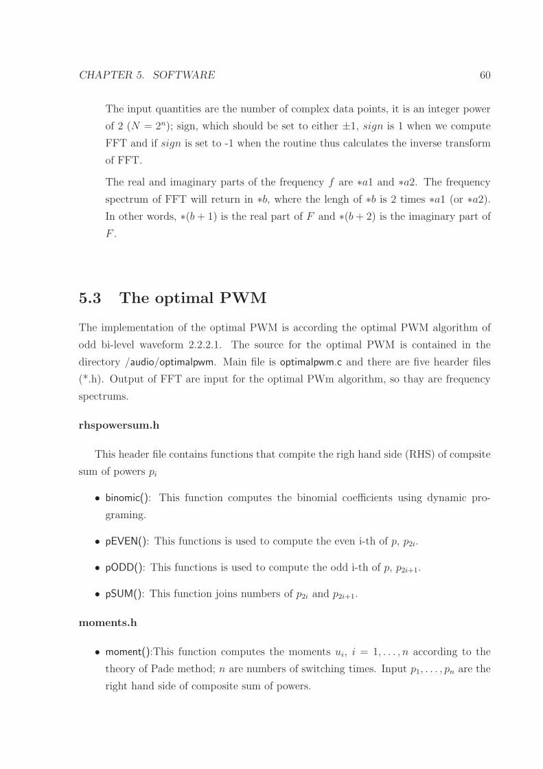
CHAPTER 5. SOFTWARE 60
The input quantities are the number of complex data points, it is an integer power
of 2 (N = 2n); sign, which should be set to either ±1, sign is 1 when we compute
FFT and if sign is set to -1 when the routine thus calculates the inverse transform
of FFT.
The real and imaginary parts of the frequency f are ∗a1 and ∗a2. The frequency
spectrum of FFT will return in ∗b, where the lengh of ∗b is 2 times ∗a1 (or ∗a2).
In other words, ∗(b+ 1) is the real part of F and ∗(b+ 2) is the imaginary part of
F .
5.3 The optimal PWM
The implementation of the optimal PWM is according the optimal PWM algorithm of
odd bi-level waveform 2.2.2.1. The source for the optimal PWM is contained in the
directory /audio/optimalpwm. Main file is optimalpwm.c and there are five hearder files
(*.h). Output of FFT are input for the optimal PWm algorithm, so thay are frequency
spectrums.
rhspowersum.h
This header file contains functions that compite the righ hand side (RHS) of compsite
sum of powers pi
• binomic(): This function computes the binomial coefficients using dynamic pro-
graming.
• pEVEN(): This functions is used to compute the even i-th of p, p2i.
• pODD(): This functions is used to compute the odd i-th of p, p2i+1.
• pSUM(): This function joins numbers of p2i and p2i+1.
moments.h
• moment():This function computes the moments ui, i = 1, . . . , n according to the
theory of Pade method; n are numbers of switching times. Input p1, . . . , pn are the
right hand side of composite sum of powers.

CHAPTER 5. SOFTWARE 61
pademethod.h
This header file is the ”heart” of the optimal PWM algorithm. It contains the method
to determine the swiching times α = (α1, . . . , αn).
• hankel(): This function defines hankel matrix created by moments ui, where i =
1, . . . , n are number of switching times
• qrdec() : This function compute QR decomposition. This is used to solve linear
Hankel system. For more see A.1.
• solvew(): This is used to solve linear system R ∗W = QT ∗B, where U = Q ∗R, U
is a upper matrix.
• solvev(): The function solves matrix equation with triangular hankel matrix.
rfpoly.h
This header file contains functions that are used Bairstow Method to find both the
real and complex roots of a polynomial. Is is based on the idea of synthetic division of
the given polynomial by a quadratic function. This approach can be used to find all the
roots of a polynomial. For more information see [22] and its pseudocode in A.2
• rootsfind(): This function extracts individual real or complex roots from list of
quadratic factors.
• deflation(): It is simply polynomial division. Suppose find a single root of an n− th
order polynomial. The effort of finding a root hopefully decreases in each step. But
the mehod cannot convergen twice to the sam non multiple root.
• quadfinder(): Find quadratic factor using Bairstow’s method (quadratic Newton
method). A number of ad hoc safeguards are incorporated to prevent stalls due to
common difficulties, such as zero slope at iteration point, and convergence problems.
• diff poly(): Differentiate polynomial a returning result in b
• recursive(): This function reduces the order of original polynomial to lower order
of all multiple roots by one, and has no other roots in common with it. If a root
of the differentiated polynomial is a root of the original polynomial, there must be
multiple roots at that location. The differentiated polynomial, however, has lower

CHAPTER 5. SOFTWARE 62
order and is easier to solve. When the original polynomial exhibits convergence
problems in the neighborhood of some potential root, a best guess is obtained and
tried on the differentiated polynomial. The new best guess is applied recursively
on continually differentiated polynomials until failure occurs. At this point, the
previous polynomial is accepted as that with the least number of roots at this
location, and its estimate is accepted as the root.
times.h
• switch time(): This function compute switching times αi according [7] in 2.2.2.
5.4 Compiling driver and aplication
In each directory is Makefile. To compile the driver is used toolchain 152-linux-2.6.34
that is set in PATH environment variable. The binary file will be usart-pwm.ko, we can
copy it to the target and load it to Linux kernel according usage at 4.5.2. The fft.c and
optimalpwm.c are applications, such as in section 4.1 so that must be compiled on the
workstation by cross-compiler toolchain. And its binary files will be loaded onto the
target boad OC8-S.In this project, the cross-compiler toolchain arm-gnueabi-gcc is used
to compile all applications 4.3. Output files are fft-arm and optimalpwm-arm, such as 4.28
we can load them onto the OC8-S.

Chapter 6
Testing and final work
In this chapter, several tests were conducted to ensure if the digital class-D audio amplfier
has any problems. We are starting with software testing: check the correctness of the
optimal PWM algorithm, calculate THD and the USART driver. The possible error
scenarios that may happen in the environment and influence the device are run through
next.
Finally, in the last section, the final embedded Linux will be configured and its image
will be deployed on the target.
6.1 Software testing
6.1.1 The optimal PWM algorithm
The optimal PWM algorithm has been already tested on the PC workstation during the
development of the digital class-D audio amplifier, no error was observed. The correctness
of switching times is proven: Therefore input data are frequency spectrums bfi , output
are switching times αi. In table 6.1 are results of computation,
63

CHAPTER 6. TESTING AND FINAL WORK 64
Table 6.1: The partial results for case n = 20, nC = 5, nE = 15, A =
10, T = 0.01 and (bf1 , bf2 , bf3 , bf4 , bf5) = (4,−5, 3, 1,−2)
i pfi µi wi vi yfi αi
0 - 1 - - - -
1 0.6858 -0.6858 -0.0005 -0.6991 -0.9905 0.0002266
2 0.3927 0.0388 -0.0007 -2.2299 0.9575 0.0004658
3 0.5877 -0.1150 0.0440 1.5471 -0.9167 0.0006929
4 0.3534 0.0283 0.0309 1.6195 0.8402 0.0009123
5 0.6318 -0.0773 -0.5062 -1.1226 0.6532 0.0011667
6 0.3093 0.0366 -0.1125 -0.3995 -0.6328 0.0013670
7 0.6822 -0.0665 1.7470 0.2848 0.4010 0.0016114
8 0.2749 0.0400 0.1004 0.0152 -0.3090 0.0018434
9 0.7239 -0.0600 -2.2778 -0.0151 0.1242 0.0020331
10 0.2485 0.0407 -0.0133 0.0002 -0.1138 0.0023018
11 0.7570 -0.0551 - - 0.9899 0.0024801
12 0.2278 0.0403 - - -0.9713 0.0026815
13 0.7834 -0.0512 - - -0.8956 0.0029176
14 0.2111 0.0394 - - 0.7431 0.0030000
15 0.8046 -0.0480 - - -0.6458 0.0036174
16 0.1974 0.0383 - - 0.5298 0.0035904
17 0.8220 -0.0453 - - 0.9067 0.0042663
18 0.1859 0.0372 - - -0.2594 0.0043457
19 0.8365 -0.0430 - - 0.2892 0.0046177
20 0.1761 0.0361 - - 0.0125 0.0047807

CHAPTER 6. TESTING AND FINAL WORK 65
0.000 0.002 0.004 0.006 0.008 0.010
-10
-5
0
5
10
time @sD
volta
ge@VD
Optimal PWM waveform
Figure 6.1: Odd bi-level PWM waveform for n = 20
0 5 10 15 20 25 30
-4
-2
0
2
4
6
harmonics
volta
ge@VD
Frequency spectrum of optimal PWM waveform
Figure 6.2: Spectrums of odd bi-level PWM waveform for n = 20
Figure 6.1 and 6.2 show the input waveform of odd signal(the symmetry property of
signal about T/2) and its computed PWM waveform for case neven = 20. It really match

CHAPTER 6. TESTING AND FINAL WORK 66
the input spectrums (bf1 , bf2 , bf3 , bf4 , bf5) = (4,−5, 3, 1,−2) plus the cutoff frequency in
the guard band and higher harmonics.
Setting of the values n and T has a big influence on a quality of signal. In table 6.2
are results for case nodd = 5.
Table 6.2: The partial results for case n = 5, nC = 1, nE = 4, A = 15, T =
0.0002 and (bf1) = (15)
i pfi µi wi vi yfi αi
0 - 1 - - - -
1 -0.7854 -0.7854 -0.4003 -0.2446 -0.4792 0.00001550
2 1 0.8084 -0.8058 -0.4221 -0.9453 0.00002135
3 -0.5890 -0.6698 0.5408 - 0.8837 0.00006590
4 1 0.6993 - - 0.7834 0.00006811
5 -0.4909 -0.5943 - - -0.5388 0.00008942
We have equation
THD(α)[%] = 100
√
√
√
√
√
√
∑n+Ni=nc+1
(
api (α)+bpi (α)
i
)2
∑nc
i=1
(
api (α)+bpi (α)
i
)2 (6.1)
It determines the total harmonic distortion (THD). It is an amplifier specification
that compares the output signal of amplifier with the input signal and measures the
level differences in harmonic frequencies between the two. The difference is called total
harmonic distortion. Total harmonic distortion is measured as a percentage, and it means
that how the output of harmonic distortion is different than the input signal. Lower
percentages are better.
The total harmonic distortion is influenced by setting of variables n : with decreasing
n THD increases exponentially that increases the distortion of signal. From Equation
6.1, we achive the minimal THD if the numenator
√
√
√
√
n+N∑
i=nc+1
(
api(α) + bpi(α)
i
)2
(6.2)
is minimal. It means the uncontrolled harmonics must be minimal or zero.
According Equation 6.1 we obtain: for n = 5, THD = [5.59%] and n = 20, THD =
[4.55%].

CHAPTER 6. TESTING AND FINAL WORK 67
6.2 Embedded PWM generator
In this section, the stability of the embedded Linux will be checked. Each test is conducted
with several input data (n, nc, A, T, bf). With the command
. / optimalpwm−arm
Table 6.3: Execute optimalpwm
the binary file of optimal PWM algorithm is executed. On the pinout R37 of OC8H,
we can observe on the oscilloscope monitor
0 2000 4000 6000 8000 10 000-1
01234
Figure 6.3: PWM output signal for n = 5
the PWM output signal with voltage range between 0 and 3.27V .
With using Mathematica to redraw mersured data, we obtain the real odd bi-level
PWM output with periodic generation for case n = 5 in the voltage range from −3.27V
to 3.27V .
0.0002 0.0004 0.0006 0.0008 0.0010
-3
-2
-1
1
2
3
Figure 6.4: Simulated odd bi-level PWM waveform for n = 5
Figure 6.5 shows the first period of the generated odd bi-level PWM waveform for
n = 5.

CHAPTER 6. TESTING AND FINAL WORK 68
0.00000 0.00005 0.00010 0.00015 0.00020
-3
-2
-1
0
1
2
3
Figure 6.5: The first period of the real PWM output signal for n = 5
It really match the odd signal beause it is symmetric about T/2 = 0.0001.
The results of the real and computed odd bi-level PWM waveform are portrayed in
Figure 6.6.
0.00000 0.00005 0.00010 0.00015 0.00020
-15
-10
-5
0
5
10
15
time @sD
volta
ge@VD
Optimal PWM waveform
Figure 6.6: The measured and computed PWM output signal fo n = 5
From the Figure 6.6 above we could see how this PWM output is formed by the
waveform generator base on value of switching times αi. But the real PWMwaveform isn’t
correctly corresponding to the computed PWM waveform. Every pulse of the real PWM
are about 2(µs) delayed than the computed PWM waveform. The reason is explained
that we used the pulse rate 5000(Hz)(period of 200(µs)) for n = 5. So this frequency is
higher than the frequency of OC8-S is used to generate the PWM output.

CHAPTER 6. TESTING AND FINAL WORK 69
Similary, if we use the slower pulse rate f = 1000(Hz) for case n = 4, nC = 1, nE =
3, A = 6 with (bf1) = (3), we obtain
Table 6.4: The partial results for case n = 4, nC = 1, nE = 3, A = 6, T =
0.001 and (bf1) = (3).
i pfi µi wi vi yfi αi
0 - 1 - - - -
1 0.6073 -0.6073 -0.3565 -0.3037 -0.7679 0.0001107
2 0 0.1844 0.3037 -0.3565 0.4642 0.0001732
3 0.7055 -0.2725 - - 0.7679 0.0003268
4 0 0.1485 - - -0.4642 0.0003893
The PWM output with the periodic generation is formed by the waveform generator
base on value of switching times αi according to table 6.4 is shown in Figure 6.7
-0.002 -0.001 0.000 0.001 0.002
-0.10.00.10.20.30.4
Figure 6.7: PWM output signal for n = 4
and Figure 6.8
0.001 0.002 0.003 0.004
-3
-2
-1
1
2
3
Figure 6.8: Simulated odd bi-level PWM waveform for n = 4
It is clear from Figure 6.9, it is really match the odd signal beause it is symmetric
about T/2 = 0.0005.

CHAPTER 6. TESTING AND FINAL WORK 70
0.0000 0.0002 0.0004 0.0006 0.0008 0.0010 0.0012
-3
-2
-1
0
1
2
3
Figure 6.9: The first period of the real PWM output signal for n = 4
The results of the real and computed odd bi-level PWM waveform are portrayed in
Figure 6.10
0.0000 0.0002 0.0004 0.0006 0.0008 0.0010-10
-5
0
5
10
time @sD
volta
ge@VD
Optimal PWM waveform
Figure 6.10: The real and computed PWM output signal for n = 4
In this case for the pulse rate f = 1000(Hz), we coud see that the real PWM output
is conresponding to the computed PWM waveform.
From results for the case n = 4, f = 1000(Hz), correctness of the optimal PWM
algorithm is proven. Using this method, we are able to generate the driven PWM output
signal. But it is limited by the power of selected hardware OC8-S. The PWM output is
generated precisely only at slower frequency, it is about f = 1000(Hz).
No failure has been observed during these tests. Switching times αi were determined
exactly and the PWM output was generated conresponding to the switching times.

CHAPTER 6. TESTING AND FINAL WORK 71
6.3 Frequent error scenarios
In the previous section, we made several tests for software applications. The embedded
Linux system that is used to develop our project isn’t thorough, its less part has to be
implemented from scratch, it has not any where verified. Thus, in the next phase of
testing we continue analyze the system’s behavior if an error occurs in the environment
of the digital class-D audio amplifier that directly influences its operation. It is important
that the system detects these errors and reacts to them by displaying an appropriate error
message and bringing itself in a consistent state.
In the following, the frequent errors scenarios are explained and for each one the
system’s behavior is described.
Loss of an NFS connection
If the device providing the NFS network share respectively the NFS service running
on it is shut down, the user has tried restart network configuration on the PC workstation
and mount again the embedded module OC8-S.
Loading and copying USART driver to kernel
Another error is loading and copying USART driver to the kernel of the embedded
Linux on OC8-S. The command
$ lsmod
Table 6.5: Show the status of modules in the Linux Kernel
shows the status of module in the Linux kernel. If the driver hasn’t been loaded to
the kernel, the user can load it into the kernel. If it already have loaded and it occurred
error,remove it.
6.4 Final work
Before the embedded device can be used as audio amplifier class-D, some steps have
to be accomplished: First, the embedded Linux configuration is cleaned up, i.e. all

CHAPTER 6. TESTING AND FINAL WORK 72
applications that are not needed for proper operation are removed. This makes the audio
amplifier image smaller that will be written to flash memory and thereby allows faster
decompressing at boot and hence faster boot time.
All processes that are automatically started after boot system and they are not re-
quired for operation of the audio amplifier class-D, are terminated. It would even impose
a large risk because it may be cause error of the embedded Linux system on the target.
Finally, this image has to be deployed onto the target. As soon as the image resides
in flash memory, the U-Boot bootloader has to be configured to automatically boot from
there. Both steps are described in section 4.4.4.

Chapter 7
Conclusion
As the final parts of this document, a summary of the work is presented in this chapter.
The aim of the project is to try to develop the digital class-D audio amplifier with a
new approach, using the optimal PWM algorithm to generating PWM like output signal.
The module OC8-S based on ARM processor architecture AT91SAM9G20 was selected
as a hardware prototype. The embedded Linux distribution that is avaible for the ARM
architecture is used here because is was already included several software componnents
inevitable for the project. And it is a familiar computing environment whose availability
on embedded systems makes it easy to build an embedded application
Software development was the main phase of this project. The start was made by
implementing the device driver for USART which provides to receive and transmite data.
We use this feature of USART like PWM controller. The best way to generate PWM
output signal is used the implemented PWM controller on the hardware. But in our
case, the AT91SAM9G20 processor doesn’t provide this PWM controller so we must use
the alterlative way to generate PWM output. It can receive input data and transmite
them to pinout on the header board OC8-H. The advantages of this solution are: First
that easy to handle the PWM output, the PWM module can run independently from the
optimal PWM algorithm. We can compute switching times αi in one program then we
can send them directly to the module. Second that an PWM kernel is developed free as
open source sostfware. Everyone who are interesting in the the optimal PWM problem
can have access to the complete source code.
Development continued with user space applications: The optimal PWM algorithm
to determine swithcing times. Firstly, it was implemeted and compiled by ARM GCC on
the PC workstation, then it was loaded on to the target board.
The aim of this project as stated in the introductory chapter ware clearly fulfilled. A
73

CHAPTER 7. CONCLUSION 74
picture of the device during operation is shown in Figure 7.1
Figure 7.1: The prototype of the digital class-D audio amplifier.
The following conclusions of the work are :
• The advantage of Linux in general is that it is free of royalties because it is open
source software. Everyone has access to the complete source code which is of high
importance when developing embedded systems.
• The embedded Linux system is a fully functional operating system which makes
software development for embedded systems much easier.
• A wide range of drivers, protocols and user space applications are available with
the embedded Linux distribution.
• The version of the embedded Linux ported to the ARM processor that was used
for the digital class-D audio amplifier was very stable, crashes of the kernel did
never happen. However, a few problems were detected in important applications
or tools. For example, the NFS server or DHCP network protocol suffered from a
programming error that leaded to a failure.

CHAPTER 7. CONCLUSION 75
• The conclusion thereof is that thoroughly testing of each application or kernel mod-
ule is a must before it is loaded on to an embedded system.
In the future, the embedded Linux sytem for ARM processor including the applications
is expected to become more and more stable. Development activity in the community is
very high.
Finally, some ideas for future enhancements of the digital class-D audio amplifier are
presented:
• The optimal PWM coding algorithm would be implemeted in programming lan-
guage more optimal.
• The USART driver would be more and more stable.
• We could use another hardware prototype to develop the audio amplifier class-D
that provides more quality and accurate PWM signal than OC8-S. For example,
FPGA.

Apendix A
Algorithms/Mathematical
Background
A.1 QR decomposition
Algorithm A.1.1: Modified Gram Schmidt(R,Q)
for k = 1 to n do
begin
s := 0;
for j := 1 to m do
s := s + a2jk
rkk = sqrt(s);
for j := 1 to m do
qjk = ajk/rkk;
for i := k + 1 to n do
begin
s := 0;
for j := 1 to m do s := s + aji ∗ qjk;
rki := s;
for j := 1 to m do aji := aji − rki ∗ qjk;
end;
end
I

APENDIX A. ALGORITHMS/MATHEMATICAL BACKGROUND II
A.2 A pseudocode algorithm for finding real and
complex roots of real polynomials with
multiple roots
1. Call Bairstow’s method with small initial estimate.
2. If convergence was satisfactory, goto [10].
3. Let D = P’.
4. If the constant term is zero, shift all coefficients down reducing order by [1].
5. If the order of D is 2, estimate is D: goto [10].
6. Call Bairstow’s method on D using estimate.
7. If convergence was satisfactory, goto [10].
8. If wrong root, restore D and previous estimate, goto [10].
9. Goto [3].
10. Deflate polynomial using estimate and save quadratic.
11. Replace original polynomial with reduced polynomial.
12. If the order of the reduced polynomial is greater than 2, goto [1].
13. Get remaining root(s) and return to caller

Apendix B
Content of the Attached CD
1. Directory 1: The sources code of aplication in *.tar.gz archive files.
• U-Boot for module OC8-S
uboot.tar.gz
• uImage for module OC8-S
uimage.tar.gz
• USART-PWM
usartpwm.tar.gz
• optimalpwm for x86
optimalwpmx86.tar.gz
• optimalpwm for oc8s
optimalpwmoc8s.tar.gz
• FFT
fft.tar.gz
2. Directory 2: Thesis
III

Bibliography
[1] Udo Zolzer, Digital Audio Signal Processing, Second Edition. A John Wiley &
Sons, 2008.
[2] P. Kujan, Wikipedia. Class D Amplifier,[Online], Available:
http://en.wikipedia.org/wiki/Class D Amplifier
[3] D. Self, R. Brice, B. Duncan, John L. Hood, I. Sinclair, A. Singmin, D. Davis,
E. Patronis, J. Watkinson, Audio Engineering. NEWNES, 2009.
[4] John Watkinson, An Introduction to Digital Audio, Second Edition. Focal Press,
2002.
[5] P. Kujan, Optimal odd single-phase multilevel problem -homepage, [Online],
Available:
http://support.dce.felk.cvut.cz/pub/kujanp/software/optimalpwm/index.html
[6] D. Self, Audio Power Amplifier Design Handbook, Fourth edition. NEWNES, 2006.
[7] Atmel Corporation: AT91SAM9G20 Preliminary, revision E, updated 2.10.
AT91SAM9G20Preliminary.pdf
[8] Open Controller: OC8S User Manual, [Online]. Available:
http://www.opencontroller.com, June 2010.
[9] Open Controller: OC8H-pinout, June 2010.
OC8H-pinout.pdf
[10] Gene Sally, Pro Linux Embedded Systems. Apress, 2010.
[11] GNU Toolchain for ARM Processors, [Online]. Available:
http://www.codesourcery.com
IV

BIBLIOGRAPHY V
[12] Open Source Initiative, [Online]. Available:
http://www.opensource.org/docs/definition.php
[13] Daniel P. Bovet, Marco Cesati, Understanding the Linux Kernel, 3rd Edition.
O’Reilly, November 2005
[14] William von Hagen, The Definitive Guide to GCC, Second Edition. Apress, 2006.
[15] Embedded Linux kernels, [Online]. Available:
www.arm.linux.org.uk
[16] Karim Yaghmour, Jo Masters, Gilad Ben- Yossef, and Philippe Gerum, Building
Embedded Linux Systems, Second Edition. O’REILLY, August 2008.
[17] BusyBox, [Online]. Available:
http://www.busybox.net
[18] Christopher Hallinan, Embedded Linux Primer: A Practical Real-World Approach.
Prentice Hall, Sept. 18, 2006.
[19] Das U-boot, [Online]. Available:
http://u-boot.sourceforge.net
[20] The Linux kernel, [Online]. Available:
http://kernel.org
[21] Thomas H. Cormen, Charles E. Leiserson, Ronald L. Rivest and Clifford Stein ,
Introduction to Algorithms, Second Edition The MIT Press, 2001.
[22] C. Bond, A Robust Strategy for Finding All Real and Complex Roots of Real
Polynomials , 2002.