IMPLANTABLE SUB-cm WIRELESS RESONATORS FOR MRI: FROM...
119
IMPLANTABLE SUB-cm WIRELESS RESONATORS FOR MRI: FROM CIRCUIT THEORY TO MEDICAL IMAGING a dissertation submitted to the graduate school of engineering and science of bilkent university in partial fulfillment of the requirements for the degree of doctor of philosophy in electrical and electronics engineering By Sayım G¨ okyar December 2017
Transcript of IMPLANTABLE SUB-cm WIRELESS RESONATORS FOR MRI: FROM...

IMPLANTABLE SUB-cm WIRELESSRESONATORS FOR MRI: FROM CIRCUIT
THEORY TO MEDICAL IMAGING
a dissertation submitted to
the graduate school of engineering and science
of bilkent university
in partial fulfillment of the requirements for
the degree of
doctor of philosophy
in
electrical and electronics engineering
By
Sayım Gokyar
December 2017
IMPLANTABLE SUB-cm WIRELESS RESONATORS FOR MRI:
FROM CIRCUIT THEORY TO MEDICAL IMAGING
By Sayım Gokyar
December 2017
We certify that we have read this dissertation and that in our opinion it is fully
adequate, in scope and in quality, as a dissertation for the degree of Doctor of
Philosophy.
Hilmi Volkan Demir (Advisor)
Ergin Atalar
Oguz Gulseren
Hatice Kader Karlı Oguz
Cengizhan Ozturk
Approved for the Graduate School of Engineering and Science:
Ezhan KarasanDirector of the Graduate School
ii
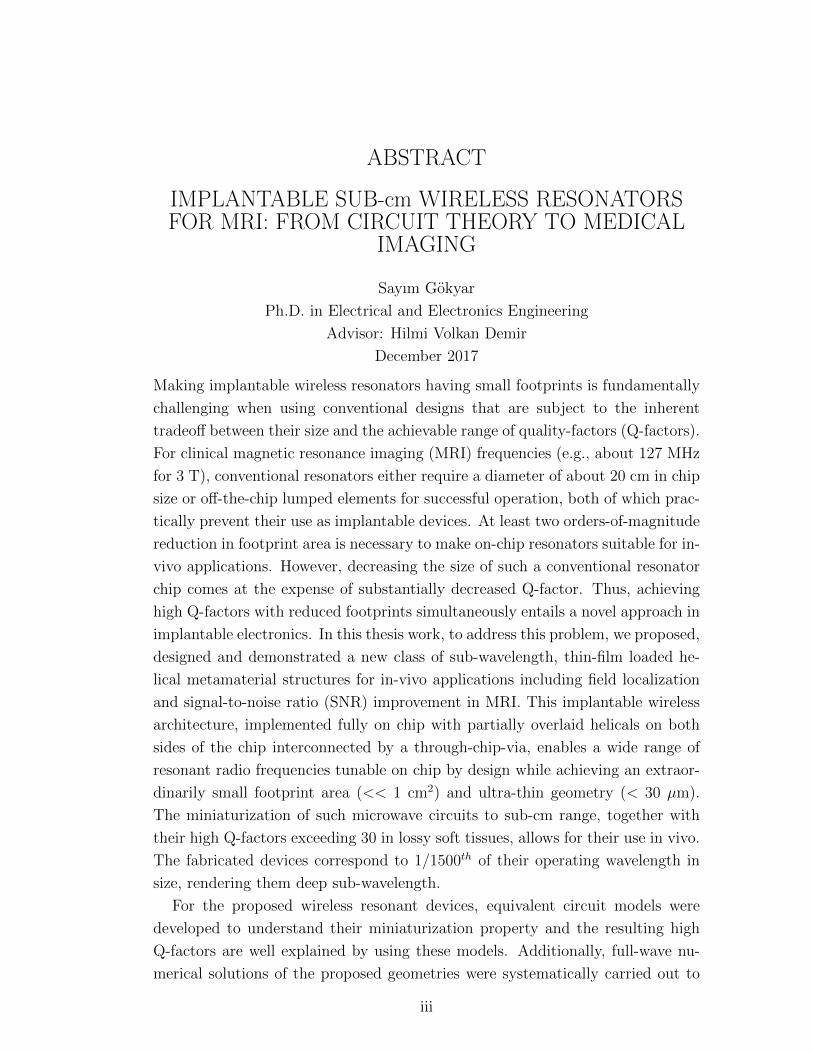
ABSTRACT
IMPLANTABLE SUB-cm WIRELESS RESONATORSFOR MRI: FROM CIRCUIT THEORY TO MEDICAL
IMAGING
Sayım Gokyar
Ph.D. in Electrical and Electronics Engineering
Advisor: Hilmi Volkan Demir
December 2017
Making implantable wireless resonators having small footprints is fundamentally
challenging when using conventional designs that are subject to the inherent
tradeoff between their size and the achievable range of quality-factors (Q-factors).
For clinical magnetic resonance imaging (MRI) frequencies (e.g., about 127 MHz
for 3 T), conventional resonators either require a diameter of about 20 cm in chip
size or off-the-chip lumped elements for successful operation, both of which prac-
tically prevent their use as implantable devices. At least two orders-of-magnitude
reduction in footprint area is necessary to make on-chip resonators suitable for in-
vivo applications. However, decreasing the size of such a conventional resonator
chip comes at the expense of substantially decreased Q-factor. Thus, achieving
high Q-factors with reduced footprints simultaneously entails a novel approach in
implantable electronics. In this thesis work, to address this problem, we proposed,
designed and demonstrated a new class of sub-wavelength, thin-film loaded he-
lical metamaterial structures for in-vivo applications including field localization
and signal-to-noise ratio (SNR) improvement in MRI. This implantable wireless
architecture, implemented fully on chip with partially overlaid helicals on both
sides of the chip interconnected by a through-chip-via, enables a wide range of
resonant radio frequencies tunable on chip by design while achieving an extraor-
dinarily small footprint area (<< 1 cm2) and ultra-thin geometry (< 30 µm).
The miniaturization of such microwave circuits to sub-cm range, together with
their high Q-factors exceeding 30 in lossy soft tissues, allows for their use in vivo.
The fabricated devices correspond to 1/1500th of their operating wavelength in
size, rendering them deep sub-wavelength.
For the proposed wireless resonant devices, equivalent circuit models were
developed to understand their miniaturization property and the resulting high
Q-factors are well explained by using these models. Additionally, full-wave nu-
merical solutions of the proposed geometries were systematically carried out to
iii

iv
verify the findings of the developed equivalent circuit models. All of these theo-
retical and numerical studies were found in excellent agreement with the experi-
mental RF characterization of the microfabricated devices. Retrieval analyses of
the proposed architectures showed that these geometries lead to both negative
relative permittivity and permeability simultaneously at their operating frequen-
cies, which do not naturally exist together in nature, making these structures
true metamaterials. These fabricated wireless devices were further shown to be
promising for the in-vivo application of subdural electrode marking, along with
SNR improvement and field localization without causing excessive heating in
MRI. MR images support that the proposed circuitry is also suitable for MRI
marking of implants, high-resolution MR imaging and electric field confinement
for lossy medium. Although our demonstrations were for the purpose of marking
subdural electrodes, RF characterization results suggest that the proposed device
is not limited to MRI applications. Utilizing the same class of structures enabling
strong field localization, numerous wireless applications seem feasible, especially
where miniaturization of the wireless devices is required and/or improving the
performance of conventional structures is necessary. The findings of this thesis
indicate that the proposed implantable sub-cm wireless resonators will open up
new possibilities for the next-generation implants and wireless sensing systems.
Keywords: Metamaterials, wireless resonators, magnetic resonance imaging
(MRI), MR-compatible implants.

OZET
MRG ICIN IMPLANT EDILEBILIR KABLOSUZcm-ALTI CINLACLAR: DEVRE TEORISINDEN TIBBI
GORUNTULEMEYE
Sayım Gokyar
Elektrik Elektronik Muhendisligi, Doktora
Tez Danısmanı: Hilmi Volkan Demir
Aralık 2017
Kucuk baskı alanına sahip implant edilebilir kablosuz rezonatorlerin (cınlacların)
yapılması, geleneksel tasarımların buyuklukleri ve ulasılabilen kalite faktorleri
aralıgı (Q-faktorleri) arasındaki iliskiye baglı olarak oldukca zorlayıcıdır. Klinik
manyetik rezonans goruntuleme (MRG) frekansları icin (ornegin 3 T icin yaklasık
127 MHz), klasik cınlaclar basarılı bir islem icin ya cip boyutunda yaklasık 20
cm’lik bir capa ya da cipten bagımsız harici elemanlara ihtiyac duyar ki; bun-
ların her ikisi de pratik olarak implant edilebilir cihazlar olarak kullanımı en-
geller. Vucut ici uygulamalarda kullanılabilmeleri icin, yonga boyutunda en az
iki basamak (100 kat) kucultme yapılması gereklidir. Bununla birlikte, boyle
bir geleneksel rezonator cipinin boyutunun bu denli azaltılması, onemli olcude
azaltılmıs Q-faktoruyle sonuclanır. Bu nedenle, baskı alanı azaltılmasının ve
yuksek Q-faktorlerinin aynı anda elde edilmesi, implant edilebilir elektronik icin
yeni bir yaklasımı gerektirir. Bu tez calısmasında, bu sorunu cozmek icin, yeni
bir sınıf olarak dalgaboyunun cok altında, ince film yuklu, sarmal meta-malzeme
yapılar onerip, tasarladık ve bunların MRG′de alan lokalizasyonu ve sinyal-
gurultu oranı (SNR) iyilestirmeyi de iceren vucut ici uygulamalarını gosterdik.
Cipin her iki tarafında kısmen ust uste konmus helezonlar ile tamamen cipte uygu-
lanan bu implant edilebilir kablosuz mimari, olaganustu kucuk bir baskı alanı
elde ederken (<<1 cm2), cok ince geometriye (< 30 µm) ve tasarımı sayesinde
ayarlanabilen genis bir yelpazede rezonant radyo frekans aralıgına olanak tanır.
Bu mikrodalga devrelerinin cm-altı aralıgına kucultulmesi, kayıplı yumusak doku-
larda 30’u asan yuksek Q-faktorleri ile birlikte vucut-ici kullanımına imkan saglar.
Uretilen cihazların boyutu calısma dalgaboylarının 1 / 1500’u buyuklugune
karsılık gelir ve boylece dalgaboyu cok altına erisilmis olur.
Onerilen kablosuz rezonant cihazların minyaturlestirme ozelliklerini anlamak
icin eslenik devre modelleri gelistirildi ve ortaya cıkan yuksek Q-faktorleri bu
v
vi
modelleri kullanarak tutarlı bir sekilde acıklandı. Buna ek olarak, onerilen ge-
ometrilerin sayısal cozumleri, gelistirilen esdeger devre modellerin bulgularını
dogrulamak icin sistematik bir sekilde gerceklestirildi. Butun bu teorik ve sayısal
calısmalar, mikro-uretilmis cihazların deneysel RF analizi ile mukemmel bir uyum
icinde bulundu. Onerilen mimarilerin calısma frekanslarında yapılan analizleri,
bu geometrilerin dogada dogal olarak bulunmayan ve bu yapıları gercek meta-
malzeme haline getiren, hem negatif nispi elektriksel sabite hem de negatif nispi
manyetik gecirgenlige sahip oldugunu gosterdi. Bu imal edilen kablosuz ciha-
zların, MRG’de asırı derecede ısınmaya neden olmadan SNR iyilestirmesi ve alan
lokalizasyonu ile birlikte dura-altı elektrot isaretlemesinin vucut ici uygulaması
icin umut verici oldugu gosterildi. MR goruntuleri, onerilen devrenin implant-
ların MR goruntulemesi, yuksek cozunurluklu MR goruntuleme ve kayıplı or-
tam icin elektrik alan yogunlastırma icin de uygun oldugunu desteklemektedir.
Gosterimlerimiz bu calısmada subdural elektrotları isaretlemek icin yapılmıs olsa
da, RF analiz sonucları onerilen cihazın sadece MRG uygulamaları ile sınırlı ol-
madıgını gostermektedir. Guclu alan lokalizasyonunu mumkun kılan aynı yapı
sınıfını kullanarak, ozellikle kablosuz cihazların minyaturlestirilmesi ve/veya ge-
leneksel yapıların performansını arttırılması gereken yerler gibi sayısız kablosuz
uygulama mumkun gorunmektedir. Bu tezin bulguları, onerilen implant edilebilir
cm-altı kablosuz cınlacların, gelecek nesil implantlar ve kablosuz algılama sistem-
leri icin yeni imknlar acılacagını gostermektedir.
Anahtar sozcukler : Metamalzemeler, kablosuz rezonatorler, manyetik rezonans
goruntuleme (MRG), MR-uyumlu implantlar.

Acknowledgement
I would like to express my appreciation to my supervisor Prof. Hilmi Volkan
Demir for his endless energy and motivating personality that propelled me to
conduct this research. He technically and mentally guided me through this long,
tough and blessed way to keep up the good work.
It is my pleasure to express sincere regards to Prof. Ergin Atalar for his
invaluable contribution to this thesis work. He opened the doors of MRI to this
research work and allowed us to use UMRAM (National MR Research Center)
for our experiments. I would like to thank my committee members, Prof. Oguz
Gulseren, Prof. Hatice Kader Karlı Oguz and Prof. Cengizhan Ozturk for their
valuable comments and guidance.
I would like to express my special thanks to each and every member (past
and present) of Devices and Sensors Research Group for their kind and eternal
friendship. I also want to thank to Biomedical Engineering Group members and
personnel of UMRAM, Department of Electrical and Electronics Engineering,
people of UNAM and ARL, members of Outdoor Sports Society (Bilkent-DOST),
Bilkent Orienteering Team (BOT) and METU Orienteering Team.
Particularly, I would like to express my thanks to Dr. Akbar Alipour, Emre
Unal, Dr. Burcak Bilginer, Dr. Oktay Algın, Dr. Somayyah Fardindoost for their
contributions throughout this thesis work. I also want to express my appreciation
to Muhammet Goncu, Ozan Kanbertay, Murat Can Yıldız, Ceren Ozveri, Elif
Tosun and Muruvet Parlakay for their support during my graduate lifetime.
This is the right time for me to declare my great appreciation to my wife and
family. There is no word to define your sacrifice. You have sustained me, you
have prayed for me and you have loved me. This work cannot be finished without
your blessing support.
This work is partially supported by TUBITAK BIDEB.
vii
Contents
1 Introduction 1
1.1 Motivation of the Thesis . . . . . . . . . . . . . . . . . . . . . . . 1
1.2 Organization of the Thesis . . . . . . . . . . . . . . . . . . . . . . 3
2 Basics of MRI 5
2.1 Electromagnetic Fields and Hardware of MRI . . . . . . . . . . . 7
2.1.1 Direct Current (DC) Field and Its Coil (or Magnet) . . . . 7
2.1.2 Gradient Fields and Their Coils . . . . . . . . . . . . . . . 8
2.1.3 Radio Frequency (RF) Fields and Their Coils . . . . . . . 9
3 Design and Demonstration of a Deep Sub-Wavelength Wireless
Resonator 14
3.1 Achieving Deep Sub-Wavelength Resonance . . . . . . . . . . . . 15
3.2 Circuit Theory Approach . . . . . . . . . . . . . . . . . . . . . . . 20
3.3 Numerical Studies . . . . . . . . . . . . . . . . . . . . . . . . . . . 28
3.3.1 Tuning a Deep Sub-wavelength Resonator . . . . . . . . . 28
3.3.2 Q-factor Analyses . . . . . . . . . . . . . . . . . . . . . . . 31
3.3.3 Loading Effect . . . . . . . . . . . . . . . . . . . . . . . . . 35
3.3.4 E- and H-Field Distributions . . . . . . . . . . . . . . . . . 40
3.4 Microfabrication . . . . . . . . . . . . . . . . . . . . . . . . . . . . 42
3.5 RF Characterization . . . . . . . . . . . . . . . . . . . . . . . . . 47
3.6 Metamaterial Characterization . . . . . . . . . . . . . . . . . . . . 57
4 MRI with Wireless Resonators 60
4.1 Intensity Distribution Maps . . . . . . . . . . . . . . . . . . . . . 61
4.2 B1 Mapping of Wireless Resonators . . . . . . . . . . . . . . . . . 63
4.2.1 Double Angle Method . . . . . . . . . . . . . . . . . . . . 64
4.2.2 Progressive Fit to Multiple Angles . . . . . . . . . . . . . . 65
viii

CONTENTS ix
4.2.3 Bloch-Siegert Method . . . . . . . . . . . . . . . . . . . . . 68
4.3 SNR Mapping . . . . . . . . . . . . . . . . . . . . . . . . . . . . . 69
4.4 SAR Distribution . . . . . . . . . . . . . . . . . . . . . . . . . . . 72
4.5 Temperature Study . . . . . . . . . . . . . . . . . . . . . . . . . . 73
4.6 Proof-of-Concept Demonstration Under 1.5 T . . . . . . . . . . . 75
5 Imaging Applications 77
5.1 MRI Marking of Subdural Electrodes . . . . . . . . . . . . . . . . 77
5.2 SNR Improvement for High-Resolution MRI . . . . . . . . . . . . 80
5.3 Other Applications . . . . . . . . . . . . . . . . . . . . . . . . . . 84
6 Conclusions 86
6.1 Contributions to the Literature . . . . . . . . . . . . . . . . . . . 89

List of Figures
2.1 Illustration of a spin (a), its quantum mechanical representation to
explain energy levels (b) and a schematic of a tissue under external
DC magnetization (c). . . . . . . . . . . . . . . . . . . . . . . . . 6
2.2 A 3 T Siemens Tim-Trio Imaging System located at UMRAM. . . 8
2.3 Illustration of an excited spin with non-zero transverse (xy) and
longitudinal (z) magnetization vectors. . . . . . . . . . . . . . . . 10
2.4 Longitudinal and transverse magnetization of a fat tissue for 1.5
T normalized to initial magnetization. . . . . . . . . . . . . . . . 12
3.1 Schematic representation of the proposed helical ring resonator. . 15
3.2 Schematics of the analyzed structures designed in the same foot-
print area (a×a) with a metallization width of w, a metallization
thickness of tmetal and a gap width of g. In addition to these param-
eters, the proposed architecture (bottom) has a dielectric thickness
of tdielectric. . . . . . . . . . . . . . . . . . . . . . . . . . . . . . . . 16
3.3 Simulation environment to obtain RF and EM characterization of
the analyzed structures. . . . . . . . . . . . . . . . . . . . . . . . 16
3.4 Resonance frequency comparison of different structures. Circle and
rectangle resonators have the same f0 of 10.6 GHz. On the other
hand, circular and rectangular split-ring resonators (SRR) have
the corresponding f0 of 6.1 and 5.2 GHz, respectively. A double
layer SRR structure, with a 0.5 mm polyimide dielectric thickness,
has the f0 of 4.7 GHz and adding a cross-via metallization drops
this resonance frequency to 0.9 GHz. There is a clear one-order-of-
magnitude shift compared to conventional resonators and 5-folds
decrease compared to SRRs and double layer counterparts. . . . . 17
x

LIST OF FIGURES xi
3.5 Frequency characterization of the proposed architecture with dif-
ferent dielectric thicknesses and metallization widths. Although
dielectric thickness has a monotonous effect on the resonance fre-
quency, metallization width has a non-linear effect on it. . . . . . 19
3.6 Schematic representation of a rectangular two-turn helical res-
onator and its equivalent circuit model for a given unit cell. . . . . 24
3.7 Schematic representation of a circular two-turn helical resonator
and its equivalent circuit model n0 unit cells. . . . . . . . . . . . . 24
3.8 Real part of the input impedance for the double-layer helical res-
onator. . . . . . . . . . . . . . . . . . . . . . . . . . . . . . . . . . 26
3.9 Resonance frequency characterization of the circular resonator us-
ing systematically varied overlap area. . . . . . . . . . . . . . . . 27
3.10 Frequency characteristics of the proposed resonator design for dif-
ferent overlapping thin-film regions. It is seen that resonance fre-
quencies of about 120 to 450 MHz is achievable by partial removal
of the overlay. . . . . . . . . . . . . . . . . . . . . . . . . . . . . . 29
3.11 Frequency tuning property of the proposed resonator architecture
for different dielectric thicknesses. It is observed that the resonance
frequencies from 70 MHz to 5.5 GHz is possible using the given
footprint area and varying dielectric thicknesses. . . . . . . . . . . 30
3.12 Q-factors of different designs for an arbitrary resonance frequency
of 250 MHz. (a) Q-factor increases due to increased overlay region.
(b) Q-factor increases due to increased dielectric thickness. . . . . 32
3.13 Schematics of the calculation domain at the resonance frequency of
250 MHz for different design parameters (not drawn to scale). (a)
A thin-film region thickness of 30 µm with a 95% of overlay area,
(b) a thin-film region thickness of 20 µm with a 63% of overlay
area, and (c) a thin-film region thickness of 10 µm with a 33% of
overlay area. . . . . . . . . . . . . . . . . . . . . . . . . . . . . . 33
3.14 Q-factors of different designs for an arbitrary resonance frequency
of 250 MHz. (a) Q-factor increases linearly due to the increased
overlay area and (b) Q-factor increases linearly due to the increased
thin-film region thickness. The overall dielectric region has a con-
stant thickness of 100 µm. . . . . . . . . . . . . . . . . . . . . . . 34

LIST OF FIGURES xii
3.15 Schematic of the calculation domain for a 3-layer resonator at a
resonance frequency of 250 MHz for different design parameters
(not drawn to scale). (a) A thin-film region thickness of 70 µm
with a 95% of overlay area, (b) a thin-film region thickness of 50
µm with a 65% of overlay area and, (c) a thin-film region thickness
of 30 µm with a 19% of overlay area. . . . . . . . . . . . . . . . . 34
3.16 Q-factors of different designs for an arbitrary resonance frequency.
Q-factor increases linearly due to increased turn ratio as expected
from cascaded-equivalent-circuit models. . . . . . . . . . . . . . . 35
3.17 Electric field confinement property of the proposed resonator archi-
tecture. (a) Amplitude of the electric field normalized to incident
field along with the dashed line marked in (b) shows that the elec-
tric field is 6 orders of magnitude higher in the localized region on
resonance with respect to the incident field. . . . . . . . . . . . . 36
3.18 Electric field confinement comparison of the proposed architecture
(a) and the conventional SRR (b). Conventional SRR is loaded
with a capacitor of 30 pF to achieve the same resonance frequency.
Electric field confinement of the proposed structure is more than
two orders-of -magnitude (2 × 10⁶/104) higher than the conven-
tional SRRs. . . . . . . . . . . . . . . . . . . . . . . . . . . . . . . 37
3.19 Electric field spill-over comparison between the proposed architec-
ture (a) and the conventional SRR (b). . . . . . . . . . . . . . . . 38
3.20 Magnetic field (left) and Electric Field (Right) distribution of
the conventional (blue curves in plots) and proposed architecture
(green and red curves) shows that the e-field of the proposed ar-
chitecture is strongly confined in the dielectric region, without de-
grading magnetic field distribution. . . . . . . . . . . . . . . . . . 39
3.21 Field Distributions: Electric field (a), and magnetic field (b) dis-
tribution of the proposed architecture. . . . . . . . . . . . . . . . 40
3.22 Magnetic field to electric field ratio (A/V) of the structure for:
resonant (a), and non-resonant (b), modes. . . . . . . . . . . . . . 41
3.23 Magnetic field to electric field ratio (A/V) of the proposed struc-
ture (a) and the conventional SRR tuned with a lumped capacitor
(b) in a lossy medium for the resonant mode of operation. . . . . 41
LIST OF FIGURES xiii
3.24 Schematic illustration for the microfabrication of the proposed res-
onator architecture onto a rigid silicon substrate by using conven-
tional methods. . . . . . . . . . . . . . . . . . . . . . . . . . . . . 43
3.25 Schematic illustration for the microfabrication of the proposed res-
onator architecture onto a rigid silicon substrate by using simplified
methods. . . . . . . . . . . . . . . . . . . . . . . . . . . . . . . . . 45
3.26 Optical photograph of the microfabricated samples on rigid sub-
strate by using simplified methods. The ease of fabrication comes
at the cost of misalignment that would result in increased reso-
nance frequency discrepancies between the numerical and experi-
mental results. . . . . . . . . . . . . . . . . . . . . . . . . . . . . . 46
3.27 Schematic representation for the microfabrication of the proposed
architecture onto a flexible substrate by using simplified methods. 47
3.28 Optical photographs of the microfabricated samples on flexible
polyimide thin-films by using simplified methods for (a) 14 mm
and (b) 8 mm side lengths. . . . . . . . . . . . . . . . . . . . . . . 47
3.29 Equivalent circuit model to characterize a wireless resonator. The
pick-up coil antenna is inductively (M) coupled to the wireless
resonator and the input impedance, Zin seen through the antenna
is measured by using a network analyzer. . . . . . . . . . . . . . . 48
3.30 Wireless resonator characterization: (a) Real part and (b) imagi-
nary part of the effective impedance and (c) the scattering parame-
ters (S11) seen through the pick-up coil. Note that having a higher
Q-factor does not guarantee to have a sharper S11 dip, which is
conventionally true for wired measurements. . . . . . . . . . . . . 50
3.31 Experimental characterization of the fabricated samples over a 14
mm × 14 mm footprint area using a polyimide thin-film with a
thickness of 12.5 µm. Eight samples (out of nine) are working and
six of them almost have the same characteristics (Samples 2, 3,
4, 7, 8, and 9) and two of them (Samples 1 and 5) have slightly
different characteristics due to fabrication imperfections. . . . . . 51
3.32 Experimental tuning results of the fabricated samples given in Fig-
ure 3.30. All of the working samples were successfully tuned to
about the imaging frequency of a 3 T MRI scanner. . . . . . . . . 52
LIST OF FIGURES xiv
3.33 Experimental characterization of samples over 8 mm × 8 mm foot-
print area using a polyimide film with a thickness of 12.5 µm. Eight
samples (out of nine) are working but three of them (Samples 2,
3, and 4) have different characteristics due to the fabrication im-
perfections. . . . . . . . . . . . . . . . . . . . . . . . . . . . . . . 53
3.34 Experimental results of the fabricated samples with 8 mm × 8
mm footprint area using a polyimide film with a thickness of 7.5
µm. Three samples (out of four) are working with slightly different
characteristics due to fabrication imperfections. . . . . . . . . . . 54
3.35 Sample-3, given in the previous figure is tuned to the targeted
frequency of about 120 MHz by partially removing top layer with
the given percentages. Experimental and numerical results are in
agreement. . . . . . . . . . . . . . . . . . . . . . . . . . . . . . . . 55
3.36 Experimental characterization of the fabricated samples over 6 mm
× 6 mm footprint area using a rigid silicon wafer with a siliconni-
tride thickness of 1 µm. Three samples (out of four) are working
with slightly different characteristics due to the fabrication imper-
fections. . . . . . . . . . . . . . . . . . . . . . . . . . . . . . . . . 56
3.37 Retrieved material parameters of the tuned resonator for MR imag-
ing: (a) the effective relative permittivity, εr, and (b) effective
relative permeability, µr, of this metamaterial architecture have
negative values around its resonance frequency. . . . . . . . . . . 58
4.1 T1 and T2 parameters of the prepared phantom. T1 was measured
to be about 140 ms and T2, to be about 88 ms. . . . . . . . . . . 61
4.2 Intensity distribution of the proposed resonator with a footprint
area of 8 mm × 8 mm. . . . . . . . . . . . . . . . . . . . . . . . . 62
4.3 Flip-angle characterization of the proposed resonator. . . . . . . . 63
4.4 Experimental B1 mapping of the proposed resonator structure by
using double angle method. . . . . . . . . . . . . . . . . . . . . . 64
4.5 MR image of the new imaging set-up with the same phantom. The
same imaging slice was acquired for different flip angles to obtain
intensity pattern. . . . . . . . . . . . . . . . . . . . . . . . . . . . 65
4.6 MRI of the same imaging set-up in the presence of the resonator.
Intensity patterns acquired from 1, 2, and 4 mm away from the
resonator are plotted to understand its characteristics. . . . . . . 66
LIST OF FIGURES xv
4.7 B1 mapping by using multiple angle method shows that Q-factor
of the resonator significantly affects the image intensity. . . . . . . 67
4.8 Bloch-Siegert signaling scheme for B1 map extraction. . . . . . . . 68
4.9 Experimental B1 map of the proposed resonator by using Bloch-
Siegert mehtod. . . . . . . . . . . . . . . . . . . . . . . . . . . . . 69
4.10 Representation of noise calculation for complex valued pixels. . . . 70
4.11 SNR of an image for NA=5 and a pixel size of 178 µm. . . . . . . 71
4.12 SNR performance of the proposed resonator for different imaging
resolution for 80 mm × 80 mm FOV: (left) without and (right)
with the resonator. . . . . . . . . . . . . . . . . . . . . . . . . . . 71
4.13 SAR distribution results of the resonator for the child data set:
(a) 1 g of averaging without resonator, (b) 1 g of averaging with
resonator, (c) 10 g of averaging without resonator, and (d) 10 g of
averaging with resonator. . . . . . . . . . . . . . . . . . . . . . . . 73
4.14 A tuned resonator loaded into a cylindrical phantom and numeri-
cally evaluated for the highest SAR regions (top left). Experimen-
tal set-up was prepared by using the same configuration with a
five fiberoptical temperature sensing lumens located properly (top
right). Here the temperature increase measured by four probes is
not significantly different than the reference probe (the fifth one),
which was located very far from the resonator (bottom). The pro-
posed resonator is expected to be RF safe [48]. . . . . . . . . . . . 74
4.15 Schematic representation of the imaging set-up (left) and the 1.5
T MRI of the resonator that is external to the phantom (right). . 76
5.1 An eight-channel open surface coil system used for ex-vivo animal
studies. . . . . . . . . . . . . . . . . . . . . . . . . . . . . . . . . . 78
5.2 Proposed electrode-marker resonator pairs placed onto the head of
a rabbit (a). These pairs, as well as the subdural electrodes without
resonators, imaged under MRI to localize them. (b) Electrode-
marker pairs are clearly marked in the MRI, where the electrodes
without markers are not visible. . . . . . . . . . . . . . . . . . . . 79

LIST OF FIGURES xvi
5.3 Kiwi fruit imaged to visualize its sub-mm features without (top
panels) and with (bottom panels) using a resonator. Increasing
resolution (decreasing pixel size) is necessary to resolve these sub-
mm features, but this reduces SNR. Hence, smaller features cannot
be clearly resolved due to noise (top row). However, using a wire-
less resonator allows us to image these sub-mm features clearly in
its vicinity (bottom row). . . . . . . . . . . . . . . . . . . . . . . . 81
5.4 MRI characterization of the tuned resonator to resolve the evenly
distributed fibers pillars, each with a diameter of 200 µm. (a) 3
T Siemens Magnetom Trio MR imaging system was used with a
head coil, loaded with a body mimicking phantom to image fibers
immersed into the phantom. (b) MRI image shows that pillars are
clearly visible and can be countable in the vicinity of the resonator
along the blue line (at 0.1 mm away from the resonator), whereas
they are not fully resolvable along the red line (at 5 mm away
from the resonator). (c) B1+ map of the wireless metamaterial
structure. (d) Red curve shows the image intensity pattern at 5
mm away from the device and the blue curve indicates the image
intensity at 0.1 mm away from the device. The blue profile clearly
resolves all 13 of these pillars. . . . . . . . . . . . . . . . . . . . . 83
5.5 MRI of hand without a resonator (left) and with a resonator (right). 84
5.6 Conventional X-ray image of a resonator loaded phantom. Both
phantom and the resonator are visible, and unlike other metallic
implants reported in the literature, the proposed device does not
cause any imaging artifacts in this platform. This guarantees the
use of conventional methods. . . . . . . . . . . . . . . . . . . . . . 85

List of Tables
2.1 Typical relaxation parameters of different tissue types under dif-
ferent magnetic field strengths. . . . . . . . . . . . . . . . . . . . 11
3.1 Comparison of conventional resonators in terms of electrical size
and resonance frequency for wireless operation. . . . . . . . . . . 18
3.2 Numerical results of the proposed equivalent circuit method for
double-layer helical resonator using different discretization order
(n0). . . . . . . . . . . . . . . . . . . . . . . . . . . . . . . . . . . 26
3.3 Resonance frequency characterization of the proposed architecture
for different overlap areas quantified by the radial angle at the
center that sees the overlap area θ(). . . . . . . . . . . . . . . . . 27
3.4 Q-factors of different designs for an arbitrary resonance frequency
of 250 MHz. . . . . . . . . . . . . . . . . . . . . . . . . . . . . . . 32
xvii
Chapter 1
Introduction
Magnetic resonance imaging (MRI) studies of human being started early 1970s,
with the seminal work of Paul Lauterbur [1]. Before MRI, nuclear magnetic
resonance (NMR) had been already in use to characterize different materials.
In 1946, two researchers, Felix Bloch from Stanford University [2] and Edward
Mills Purcell from Harvard University [3], independently reported the first NMR
identification of materials for liquids and solids, which was awarded a Nobel
Prize in Physics [4]. This starting point turned into a medical imaging platform
with the work of Lauterbur, which was also awarded a Nobel Prize in 2003 [5].
The relatively safe nature of MRI made it indispensable part of today′s medical
imaging applications. Additionally, this opened a huge research field and today
MRI practice has been still being developed.
1.1 Motivation of the Thesis
Obtaining high-resolution MRI with a high signal-to-noise-ratio (SNR) and short
acquisition time is a challenging task for clinical applications. In addition to
proper pulses, this requires novel coil designs with improved levels of radiofre-
quency (RF) performance such as a high quality-factor (Q-factor). The motiva-
tion of this thesis is to propose and develop a novel wireless resonator architecture
1

to improve clinical MR imaging practice in terms of SNR improvement and mark-
ing of implantable devices for possible in-vivo applications.
Although the soft tissue contrast of MRI [1] is its ultimate property from
its beginning, which makes MRI the strongest candidate among characteristic
imaging modalities (including X-ray, CT, and PET), positioning of devices under
MRI requires special treatments including the use of wired connections [6–11],
introducing MRI marker materials [12–17] and using wireless passive devices with
inductive coupling [18,19].
Using wired connections to electrically reach devices under MRI is possible
for interventional applications [9], but this comes at the cost of increased RF
heating risk [20]. Using MRI visible marker materials, such as bearings and dyes
[15–17], introduces other disadvantages such as size and non-adjustable relaxation
parameters. These markers have sizes of several mm′s in three dimensions [21]
that limit their in-vivo usage for most of the clinical applications, e.g., in subdural
electrode marking. Additionally, once they are manufactured, longitudinal (T1)
and transverse (T2) relaxation times of these markers are constant and their
visibility will strictly depend on the MR imaging parameters such as repetition
time (TR) and echo time (TE). This may limit the imaging methods; hence,
additional scans with proper TR and TE values should be performed for marking
of these devices. Simultaneous imaging of marking materials and anatomical
features is critical to achieve better registration accuracy [22].
In addition to these methods, multimodal imaging is also used to mark the
locations of these implantable devices [23–26]. However, combined registration of
images that are acquired from different platforms results in reliability problems
due to higher positioning errors from 1 to about 3 mm [27, 28]. In addition to
reliability problems, moving patients from one platform to another would also
decreases the patient comfort and increases the risk of inflammation. The abil-
ity of imaging implantable devices only under MRI would avoid the need for
multimodal imaging platforms that would result in improved clinical practice.
The use of wireless resonant devices is a promising approach to mark im-
plantable devices preventing the need for multimodal imaging. MRI performance
of these wireless markers is loosely dependent on the imaging parameters (e.g.,
TR, TE and pixel volume). However, this class of devices calls for novel resonator
2
designs for proper operation. Physical dimensions of these markers together with
RF safety concerns should be considered for the surrounding tissues [20]. De-
creasing RF power is a good practice to protect patients from the harmful effects
of RF exposure but this lowers SNR on the acquired MR images and decreases
the reliability of the images for diagnosing purposes especially for the regions
with lower proton densities.
In this thesis work, we designed and demonstrated an innovative self-resonating
structure that is intended to alleviate the aforementioned complications of the
previous works in the literature. This proposed structure can be used as a wireless
MRI marking device for potential in-vivo studies such as marking of subdural
electrodes. Although it was demonstrated to mark the subdural electrodes as
a proof of concept in this thesis work, characterization results show that it is
not limited to MRI applications but also other wireless applications including
miniaturization of wireless devices and improving the performance of conventional
structures with field localization.
Here we address the scientific challenge of achieving low footprint area and
high Q-factor at the same time for 123 MHz of self-resonance frequency. As a
proof of concept demonstration we achieved an 8 mm × 8 mm footprint area
with a free-space Q-factor of about 80 for the given operational frequency. We
also report the simulation results of specific absorption rate (SAR) increase in
brain. MR images support that the proposed architecture is a potential candidate
for various applications including MRI marking of implants, high-resolution MR
imaging and E-field confinement for lossy medium applications. These features
may open up new possibilities for the next-generation implants as wells as for
new sensing systems.
1.2 Organization of the Thesis
This thesis starts with a short introduction to MRI presenting its fundamental
operating principles and imaging methods (Chapter 2). This brief introduction
prepares readers to be familiar with the relationship between the material types
and their MRIs. The thesis continues with explaining the electromagnetic fields
of MRI and their coils for imaging. A relatively detailed analysis of RF fields
3
emphasizes the importance of resonance for MRI.
In Chapter 3, methods of achieving deep-subwavelength resonance are ana-
lyzed and for the proposed thin-film loaded helical metamaterial architecture with
comparison to conventional devices reported in the literature. Here, a equivalent
circuit model is also provided to estimate the characteristics of the proposed
structure in this chapter. Numerical studies are reported to verify the results of
this equivalent circuit model. Superiority of the proposed architecture (in terms
of Q-factor, tuning performance, electric and magnetic fields, and the loading
performance) over conventional structures (such as ring resonators, split-ring res-
onators and stacked resonators) are also discussed in a comparative manner. The
microfabrication of the proposed devices is explained with necessary recipes to
highlight the suitability of the proposed architecture for mass-production. Ex-
perimental RF characterization of the microfabricated resonators and numerical
simulations of the proposed structures are included in the end of this chapter.
Chapter 4 introduces the experimental MRI characterization of the proposed
resonator for various imaging configuration. Intensity distribution maps are
provided for qualitative analyses followed by more quantitative characterization
methods including B1 mapping, SNR mapping, specific absorption rate and ther-
mal analyses under MRI. This part also includes an experimental 1.5 T study for
a proof of concept demonstration.
Next, Chapter 5 exploits some of the MRI problems frequently dealt with
in clinical environment. These include MRI marking of implantable devices
(subdural electrode marking for epilepsy treatment), SNR improvement for high-
resolution MRI applications and SNR improvement for extremities. Multimodal
imaging potential of the proposed architecture (such as imaging of this MRI com-
patible architecture with an x-ray platform) is explored to show a proof of concept
demonstration. Finally, in Chapter 6 the thesis is completed with concluding re-
marks, future outlook and a summary of the contributions of the author to the
literature.
4

Chapter 2
Basics of MRI
Early history of NMR, which has led scientists to invent MRI, starts with the
definition of Larmor frequency. Joseph Larmor (1857), an Irish physician, found
a formula to define the relationship between the external magnetic field and the
rotational frequency of a spin as given in Equation (2.1).
w = γ B (2.1)
Here, B is the magnetic field intensity (T), γ is the gyromagnetic ratio (Hz/T)
and ω is the angular frequency (rad/s) of the nuclei. Sensitivity of an atom is
defined as the ratio of MRI signal emitted from an atom to the excitation signal.
It is depicted that the MRI sensitivity of 1H is the highest compared to any other
atom [29]. Abundance of 1H atoms in tissues, together with its higher sensitivity,
makes 1H the strongest candidate to be used for clinical MRI applications. This
dominant character of 1H also has affected the MRI instrumentation with its
specific resonance frequency characteristics. A clear understanding of NMR is
necessary to figure out the basic principles of MRI, which is described as the
behavior of a nucleus under a certain magnetic field. Although the details of
NMR can be accurately explained by quantum mechanics, classical mechanics can
also be used to illustrate this phenomenon. Here, we will use a hybrid approach
to explain necessary details of NMR.
1H atom will possesses a spinning frequency determined by external magnetic
field as described in Equation (2.1). In a non-magnetized tissue, these spins are
5
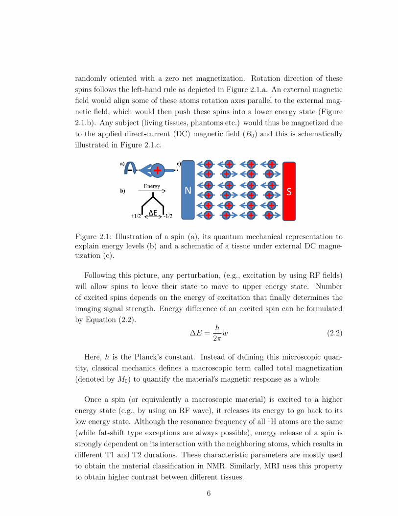
randomly oriented with a zero net magnetization. Rotation direction of these
spins follows the left-hand rule as depicted in Figure 2.1.a. An external magnetic
field would align some of these atoms rotation axes parallel to the external mag-
netic field, which would then push these spins into a lower energy state (Figure
2.1.b). Any subject (living tissues, phantoms etc.) would thus be magnetized due
to the applied direct-current (DC) magnetic field (B0) and this is schematically
illustrated in Figure 2.1.c.
Figure 2.1: Illustration of a spin (a), its quantum mechanical representation toexplain energy levels (b) and a schematic of a tissue under external DC magne-tization (c).
Following this picture, any perturbation, (e.g., excitation by using RF fields)
will allow spins to leave their state to move to upper energy state. Number
of excited spins depends on the energy of excitation that finally determines the
imaging signal strength. Energy difference of an excited spin can be formulated
by Equation (2.2).
∆E =h
2πw (2.2)
Here, h is the Planck’s constant. Instead of defining this microscopic quan-
tity, classical mechanics defines a macroscopic term called total magnetization
(denoted by M0) to quantify the material′s magnetic response as a whole.
Once a spin (or equivalently a macroscopic material) is excited to a higher
energy state (e.g., by using an RF wave), it releases its energy to go back to its
low energy state. Although the resonance frequency of all 1H atoms are the same
(while fat-shift type exceptions are always possible), energy release of a spin is
strongly dependent on its interaction with the neighboring atoms, which results in
different T1 and T2 durations. These characteristic parameters are mostly used
to obtain the material classification in NMR. Similarly, MRI uses this property
to obtain higher contrast between different tissues.
6

Although relaxation parameters are strong clues for material classification,
they are not enough for imaging. This requires additional engineering of electro-
magnetic waves, called gradient fields. In addition to DC fields for magnetiza-
tion of tissues and RF fields for perturbation of spins, gradient fields cause local
magnetic field intensity variation to allow spins to rotate at slightly different fre-
quencies. Thus, the frequency encoding of the acquired signals results in spatially
decoded data, called magnetic resonance image.
2.1 Electromagnetic Fields and Hardware of
MRI
As discussed earlier, 1H atom, which is abundant in all organic tissues, plays the
key role in determining the operating MR frequency with its specific gyromagnetic
ratio (γ = 42.58 MHz/T). Commercially available MRI scanners with B0 field
strengths from 0.1 to 4 T with the corresponding hydrogen resonance frequencies
from 4.26 to 170 MHz are used for todays clinical applications . In addition to
clinical MRI scanners, NMR scanners with B0 field strengths of up to 25 T are
used for material identification.
Depending on typical B0 values of scanners, the imaging frequency falls within
the RF range where the tissue absorption of electromagnetic (EM) power is con-
veniently very low (e.g., compared to X-ray imaging). The photography of a 3 T
Siemens Tim Trio scanner, which was located at National Magnetic Resonance
Research Center (UMRAM [30]), is provided in Figure 2.2. Traditional MRI sys-
tems provide three different magnetic fields known as DC, gradient and RF fields
that are created by three different coil systems.
2.1.1 Direct Current (DC) Field and Its Coil (or Magnet)
In opreation, rotation axes of the spins are oriented in the direction of DC mag-
netic field. Magnetization vector of nuclei under the DC magnetic field B0 will
point the given B0 direction. This configuration, quantum mechanically, means
to have a lower energy state for the spins, resulting in nonzero net macroscopic
7

Figure 2.2: A 3 T Siemens Tim-Trio Imaging System located at UMRAM.
magnetic moment (M0). For the sake of reference, direction of B0 is commonly
taken as the z direction; hence B0 notation will be used to refer to B0. Here,
it is worth pointing out that the given B0 field does not cause any excitation to
spins. At this point, any subject under DC field will only have magnetized spins
rotating with a given Larmor frequency (see Figure 2.1.c).
DC magnetic field strength determines the resonance frequency of the given
MRI system, which is considered as the identity of the system. Since permanent
magnets cannot exhibit higher field strengths, they are mostly used for open coil
scanners employed for the patients with claustrophobia. For higher field strengths
(e.g., above 0.5 T), an electromagnet, which is most commonly in the form of a
superconductor solenoid coil, is used for DC field creation [31]. As a last remark,
these coils should be continuously working during the scanner lifetime. Hence,
they are never turned off after regular operation.
2.1.2 Gradient Fields and Their Coils
After proper excitation of materials, which will be explained in the next section,
classification of these materials can be achieved by using characteristic coefficients
such as γ, T1 and T2. To obtain proper imaging signal, a relationship between
space and signal should be achieved. Any spatial non-uniformity in the DC
magnetic field will result in different resonance frequencies for the consecutive
spins, resulting in non-zero bandwidth for the acquired signals. Corresponding
8

resonance frequency differences will be used to map spins in frequency domain.
The frequency spectrum of the acquired signals will be converted to space domain
images by using Fourier transform.
This phenomenon was first proposed by Paul Christian Lauterbur and Peter
Mansfield that introducing gradient fields into the imaged medium would make
it possible to acquire the locations of emitted signals. It was the beginning of
70s when Lauterbur first obtained the first medical MRI image [1]. The detailed
mathematical expressions related to the gradient fields and RF excitation can be
found in [29].
To provide an arbitrary slice selection profile, gradient coils should be designed
in such a way that the gradient fields can be applied in any direction with any
amplitude. This is achieved by using different gradient coils for different direc-
tions. Arbitrary slice selection profile can be achieved by proper control of these
coils; hence, these coils should be turned on and off very quickly. Dimensions
of these coils are comparable with the DC coils, and thus they have very high
inductance that can create high voltages in the case of instant current deviations.
Sophisticated circuitry and various physical designs including shielding of coils
are used to provide solutions to these problems [32].
2.1.3 Radio Frequency (RF) Fields and Their Coils
Time-varying electromagnetic fields, called RF fields, are used for the excitation of
spins. Without RF fields, we only have the magnetized spins (due to DC magnetic
field), with proper frequency encoding (due to space-dependent gradient fields).
In addition to spinning of nuclei with Larmor frequency, an additional rotation
movement of these spins is added to the system with the same frequency. Now
the combination of these two movements, namely the rotation along with the B0
direction and spinning along with the rotation direction, results in coherent signal
emission from the magnetized material.
This is illustrated in Figure 2.3 that the overall magnetization of spin is now
divided into two parts, namely longitudinal ( ~Mz) and transverse magnetization
9

Figure 2.3: Illustration of an excited spin with non-zero transverse (xy) andlongitudinal (z) magnetization vectors.
( ~Mxy) as expressed in Equation (2.3).
~M0 = ~Mz + ~Mxy (2.3)
where, ~Mxy can be decomposed into its components as given in Equation (2.4):
~Mxy = Mxi+My j (2.4)
Here, ~Mz will determine the amount of signal that will be captured by the
receiver antennas. The received signal, also named as the relaxation signal, will
last for a certain amount of time. The energy stored in the excited material will
be released by the relaxation of the nuclei for a finite period of time. The Bloch
equation to define the overall magnetization in time domain is given by Equation
(2.5):
d ~M
dt= ~M × γ ~B − Mxi+My j
T2− (Mz −M0)~k
T1(2.5)
where ~M is the overall magnetization, ~B is the effective magnetic field strength,γ
is the gyromagnetic ratio of the nuclei, M0 is the initial magnetization due to
static magnetic field, T1 is the longitudinal relaxation time constant and the T2
is the transverse relaxation time constant for the materials. By assuming that
the transverse and longitudinal magnetization vectors are decoupled from each
10

other, Equation (2.5) can be solved by separating these two scalar differential
parts as given in Equation (2.6) and Equation (2.8):
dMz
dt= −Mz −M0
T1(2.6)
with a solution, after 90 excitation:
Mz(t) = M0(1− e−t/T1) (2.7)
anddMxy
dt= −Mxy
T2(2.8)
with a solution, after 90 excitation:
Mxy(t) = M0e−t/T2 (2.9)
Time-invariant magnetic field in the z-direction results in the recovery of initial
magnetization after a certain amount of time. Similarly, transverse magnetization
will die out after a certain amount of time due to the emission of magnetic
resonance signal. Typical relaxation signals for some of the tissues are given in
Table 2.1 for both 1.5 and 3 T magnetic field strengths [29].
Table 2.1: Typical relaxation parameters of different tissue types under differentmagnetic field strengths.
1.5 T 3 TTissue T2 (ms) T1 (ms) T2 (ms) T1 (ms)
Gray matter 100 900 100 1820White matter 92 780 70 1084
Muscle 47 870 45 1480Fat 85 260 83 490
Liver 43 500 42 812
Here, we can see that the T2 parameters of various types of tissues are more or
less the same for different field strengths, which shows that the transverse relax-
ation is mainly dependent on material type and intermolecular interactions rather
than the field strength. On the other hand, T1 relaxation is strictly dependent
on the field strength that is reasonable due to the effect of main magnetic field on
longitudinal direction. As an example, the longitudinal and transverse relaxation
11
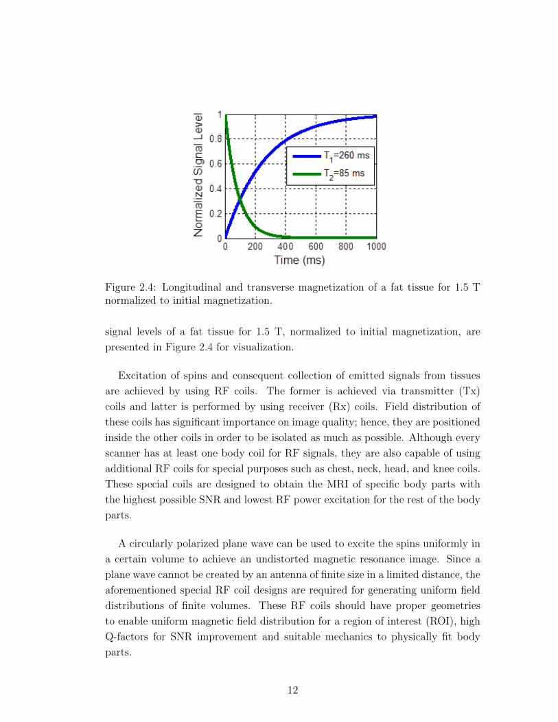
Figure 2.4: Longitudinal and transverse magnetization of a fat tissue for 1.5 Tnormalized to initial magnetization.
signal levels of a fat tissue for 1.5 T, normalized to initial magnetization, are
presented in Figure 2.4 for visualization.
Excitation of spins and consequent collection of emitted signals from tissues
are achieved by using RF coils. The former is achieved via transmitter (Tx)
coils and latter is performed by using receiver (Rx) coils. Field distribution of
these coils has significant importance on image quality; hence, they are positioned
inside the other coils in order to be isolated as much as possible. Although every
scanner has at least one body coil for RF signals, they are also capable of using
additional RF coils for special purposes such as chest, neck, head, and knee coils.
These special coils are designed to obtain the MRI of specific body parts with
the highest possible SNR and lowest RF power excitation for the rest of the body
parts.
A circularly polarized plane wave can be used to excite the spins uniformly in
a certain volume to achieve an undistorted magnetic resonance image. Since a
plane wave cannot be created by an antenna of finite size in a limited distance, the
aforementioned special RF coil designs are required for generating uniform field
distributions of finite volumes. These RF coils should have proper geometries
to enable uniform magnetic field distribution for a region of interest (ROI), high
Q-factors for SNR improvement and suitable mechanics to physically fit body
parts.
12

Although several coil geometries for different body parts have been already
designed for ex-vivo MRI, in-vivo coil designs are limited due to the difficulties
of achieving low resonance frequencies for small sizes and providing high enough
Q-factor in loaded scenarios.
To obtain the magnetic field distribution of a coil with a current distribution
of ~J , one has to solve the Equation (2.10) for every point in space (~R).
~B(~ )r =µ0
4π
∫ ~J × ~R
R3(2.10)
For Tx coils, current distribution can be obtained relatively easily due to the
known conductive geometry of the coils. But, the calculation of induced currents
on receiver coils and tissues does not have closed form solutions for most of the
geometries; thus, the use of numerical methods is unavoidable to derive magnetic
field distribution of different coil geometries.
13
Chapter 3
Design and Demonstration of a
Deep Sub-Wavelength Wireless
Resonator
Designing wireless devices in the form of resonators is of significant importance
for in-vivo applications. These devices can be used for different purposes includ-
ing in-vivo strain sensing [33, 34, 38], stent lumen visualization [19], marking of
implantable devices [18], miniaturization of antennas [39] and SNR improvement
in their close vicinities [40]. Squeezing the electrical size of a resonator down
to 1/1000 of its free space wavelength (λ0/1000) is, however, a challenging task.
One can consider different methods for this purpose including lumped element
loading [41], introducing additional turns for spirals [39], stacking different lay-
ers [42] and creating thin-film capacitances [43]. Although these methods are
acceptable for most of the conventional applications (e.g., printed circuit board
devices, tuning of antennas, waveguides, wired systems and on-board radiative
elements), in-vivo devices requirea a complex set of properties and functionalities
including bio-compatibility, flexibility, elimination of lumped elements, field con-
finement for safer operation, stable operation under lossy medium loading and
proper magnetic field manipulation for MRI among others [44].
We found that all of the above difficulties and complications can be addressed
by conceiving and developing a new class of helical ring resonators, which are
14

expected to be easy to fabricate. Potential applications including in-vivo MRI
marking and SNR improvement can be achieved in certain MRI studies using this
class of resonators [45–48]. A schematic of the proposed design is given in Figure
3.1.
Figure 3.1: Schematic representation of the proposed helical ring resonator.
Following sections provide the detailed analyses of the proposed architecture,
starting from miniaturization to experimental RF characterization along with
detailed numerical studies for better understanding of electromagnetic operation.
3.1 Achieving Deep Sub-Wavelength Resonance
Full-wave solutions are useful for providing a physical explanation to the operating
principles of resonators. This is also a cheap and convenient way to validate a
model before its fabrication. Traditional split-ring resonators (SRR) are analyzed
for their resonance frequencies (f0) to compare the results with the proposed
architecture. Schematics of the analyzed architectures are given in Figure 3.2.
To make a fair comparison among these different designs (e.g., circular and
rectangular resonators, circular and rectangular SRRs, and proposed helical split-
ring resonator architecture), we set the footprint area to 8 mm × 8 mm (side
length, a, equal to 8 mm for rectangular ones and outer radius equals to 4 mm
for circular ones), metallization thickness, tmetal, of 10 µm, a gap width, g, of 0.5
mm and a metallization width, w, of 1 mm. Here, a polyimide material from the
numerical solver library is used as the dielectric layer with a variable thickness
(tdielectric) and gold (Au) is used as the metal layer with a variable metallization
width (w).
15

Figure 3.2: Schematics of the analyzed structures designed in the same footprintarea (a×a) with a metallization width of w, a metallization thickness of tmetaland a gap width of g. In addition to these parameters, the proposed architecture(bottom) has a dielectric thickness of tdielectric.
Figure 3.3: Simulation environment to obtain RF and EM characterization of theanalyzed structures.
16
For numerical solutions, we used CST-Design StudioTM (Darmstadt, Ger-
many) to acquire scattering parameters and deduce resonance frequency from
these scattering parameters. Figure 3.3 depicts the simulation environment for
the proposed structure with two ports located in the z-direction and labeled as
1 and 2 consecutively. To obtain the resonance frequency of the wireless res-
onators, we used two wave-guide ports to acquire scattering parameters (S11 and
S21), with boundary conditions of perfect-electrical-conductor (PEC), perfect-
magnetic-conductor (PMC) and perfectly matched layer (PML) in x, y and z di-
rections, respectively. Simulation environment was extended with the side length
of the resonator (e.g., 8 mm in this case) in all directions.
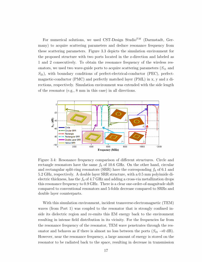
Figure 3.4: Resonance frequency comparison of different structures. Circle andrectangle resonators have the same f0 of 10.6 GHz. On the other hand, circularand rectangular split-ring resonators (SRR) have the corresponding f0 of 6.1 and5.2 GHz, respectively. A double layer SRR structure, with a 0.5 mm polyimide di-electric thickness, has the f0 of 4.7 GHz and adding a cross-via metallization dropsthis resonance frequency to 0.9 GHz. There is a clear one-order-of-magnitude shiftcompared to conventional resonators and 5-folds decrease compared to SRRs anddouble layer counterparts.
With this simulation environment, incident transverse-electromagnetic (TEM)
waves (from Port 1) was coupled to the resonator that is strongly confined in-
side its dielectric region and re-emits this EM energy back to the environment
resulting in intense field distribution in its vicinity. For the frequencies far from
the resonance frequency of the resonator, TEM wave penetrates through the res-
onator and behaves as if there is almost no loss between the ports (S21 →0 dB).
However, near the resonance frequency, a large amount of energy is stored on the
resonator to be radiated back to the space, resulting in decrease in transmission
17

parameter (S21 <0 dB). From the dip of S21, we can clearly determine the reso-
nance frequency of the resonator. Figure 3.4 depicts the results for comparison.
Here, conventional circular and rectangular resonators have the same resonance
frequency of 10.6 GHz, which is due to the traveling wave mode of the E-field.
On the other hand, creating a gap region results in different resonance frequen-
cies for these resonators as reported earlier [49]. These are 6.1 and 5.2 GHz for
the circular and rectangular SRRs, respectively. The mean electrical path for
the induced wave is different for these two geometries, which leads to different
resonance frequencies. For the stacked double-layer rectangular resonator config-
uration, thin-film capacitance between consecutive layers becomes dominant and
decreases the resonance frequency of the overall structure. In addition to thin-
film capacitance, mutual coupling of these consecutive layers can be increased by
adding a cross via metallization to the system. Thus, resulting in much lower
resonance frequency, that is about 5 times (4.7/0.9=5.2) lower compared to the
stacked geometries [51]. These results are summarized in Table 3.1.
Table 3.1: Comparison of conventional resonators in terms of electrical size andresonance frequency for wireless operation.
Resonator Type Resonance Frequency Free Space(8 mm × 8 mm) (GHz) Wavelength Electrical Size
(λ0,mm)Circular 10.6 28.2 λ0/3.5
Rectangular 10.6 28.2 λ0/3.5Circular SRR 6.1 49.3 λ0/6.2
Rectangular SRR 5.2 57.7 λ0/7.2Stacked SRR 4.7 64.1 λ0/8.0Helical SRR 0.9 327 λ0/41.0
The obvious miniaturization property of the proposed architecture makes it
the strongest candidate among other structures for in-vivo applications. To apply
equivalent circuit models, electrical size of a structure should be well below (e.g.,
10 times) of its free space resonance frequency. The most suitable structure, to
be modeled by using equivalent circuits, is the proposed helical SRR geometry.
Although there are several articles in the literature to model SRRs with suitable
equivalent circuits [49,50], they are not suitable for the proposed architecture in
here due to its dominant thin-film characteristics and increased mutual coupling.
18

Hence, the equivalent circuit model of the proposed helical SRR with distributed
thin-film loading scheme is derived from the scratch.
The superiority of the presented architecture compared to conventional struc-
tures motivates us to continue our systematic study to investigate its charac-
teristics in detail. To understand the effect of tdielectric and w on the resonance
frequency, they were systematically swept over a range of values. Figure 3.5 shows
the behavior of the proposed architecture for the same footprint area that was
given previously and with a polyimide dielectric thin film with different thick-
nesses.
Figure 3.5: Frequency characterization of the proposed architecture with differentdielectric thicknesses and metallization widths. Although dielectric thickness hasa monotonous effect on the resonance frequency, metallization width has a non-linear effect on it.
Figure 3.5 shows that decreasing the dielectric thickness allows us to reach the
lower range of resonance frequencies. When we compare these results with the
previous results (500 µm dielectric thicknesses with 1 mm of w leading to 918
MHz), here, 5 µm dielectric thickness with the same metallization width results
19

in 94 MHz resonance frequency. Results show that the resonance frequency of
the structure is linearly proportional to the square root of the dielectric thickness
(f0 ∝√tdiel).
On the other hand, increasing the metallization width does not yield a
monotonous contribution to the resonance frequency. For an infinitely thin met-
allization width, we do not expect any thin-film capacitance; hence, a higher
resonance frequency can be acceptable. When we start increasing the metal-
lization width, we introduce thin-film capacitance to the structure, which is the
main reason of lower resonance frequency. On the other hand, according to the
asymptotical equation of inductance (Leff ∝ ln( lw+tmetal
)), logarithmic term be-
comes dominant and the effective inductance terms starts to decrease. According
to Equation (3.1), combination of these two effects (increase in thin-film capac-
itance and decrease in effective inductance) generate a minimum f0. For the
Figure 3.5, we observed that the minimum resonance frequency can be achieved
for the 1 mm of metallization width. It can be concluded that the w/a ratio of
0.125 is an optimal point for rectangular and circular helical resonators to achieve
the lowest resonance frequency.
3.2 Circuit Theory Approach
For the electrical sizes of less than 1/10th of the operating wavelength (e.g., for
a resonator with a side length < λ0/10), circuit theory approach can be used
to determine the initial characteristics of a resonator. Proper modeling of effec-
tive inductance (Leff ) and effective capacitance (Ceff ) is enough to predict the
resonance frequency of a resonator, whereas the modeling of effective resistance
(Reff ) is necessary for Q-factor determination. Traditional split-ring-resonator
(SRR) designs are modeled with an effective inductance of single turn (Leff ) and
effective capacitance of the overall geometry (Ceff ).
Although asymptotic formulations for the determination of Leff is proposed for
most of the geometries [52], pre-determination of effective capacitance is not that
simple due to gap dimensions, fabrication imperfections, frequency dependent
field localizations on resonators, and fringe field calculation deficiency between
metallization layer and substrate. Since a larger capacitance is required to lower
20

the operating frequency of a resonator, these problems become more dramatic,
due to the dominant effect of capacitance.
Here, we modeled the proposed design as a series resonator with effective
parameters of Leff , Ceff and Reff . Resonance frequency, f0, of such a resonator
is given by Equation (3.1):
f0 =1
2√LeffCeff
(3.1)
and the Q-factor is given by Equation (3.2):
Q =2πf0LeffReff
=1
Reff
√LeffCeff
=f0f3dB
(3.2)
where f3dB is the full-width-half-maximum (FWHM) bandwidth of the resonator.
To design a resonator with higher Q-factors, it is necessary to increase effective
inductance and decrease the effective resistance and capacitance. For a given
frequency, f , effective RF resistance can be calculated using Equation (3.3):
Reff =l
Wσδ(1− e−tmetal/δ)(3.3)
where l is the mean path length along with the resonator, W is the metallization
width, tmetal is the thickness of the metallization, σ is the conductivity of the metal
used for fabrication, and δ is the skin-depth of the metal for the given frequency,
which is formulated as in Equation (3.4):
δ =
√2
2πfµσ(3.4)
Effective inductance can be defined as the amount of magnetic energy stored
in a volume for a given current distribution. Its analytical formulation is given
by Equation (3.5):
Leff =1
I
∮S
B · dS (3.5)
where I is the current on the conductor, S is the surface area covered by the
resonator itself and B is the magnetic flux density passing through the surface
S. A proper inductance formulation for a rectangular loop is given by Equation
(3.6) [52]:
Leff = µ0µr l [ln(l
W + tmetal) + 1.193 +
W + tmetal3l
] (3.6)
21

where µ0 is the permeability of the free space and µr is the relative permeability
of the material used for resonator fabrication (which has to be unity for MRI
operation), W is the metallization width and tmetal is the metallization thickness
for the planar inductors. When the above equation is dimensionally analyzed,
for the constant W and tmetal, the relationship between the inductance and side
length of a resonator becomes as given in Equation (3.7):
L ∝ l ln(l) (3.7)
Equation (3.7) reveals the main point for higher inductance values. If the
size of a resonator is longer, its inductance, thus the Q-factor, becomes higher.
Therefore, having higher Q-factors using smaller resonator footprint area is a
challenging task due to this limitation.
Effective capacitance of a resonator strictly depends on the metallization ge-
ometry and the ground plane location. For the resonators without clear ground
plane, e.g., SRRs fabricated on insulators, effective capacitance comes from the
summation of lumped elements (lumped capacitors if they exist) and thin-film
capacitances (due to gap region and metallization surface). From circuit theory
approach, increasing capacitance is not desired due to the effect of decreased Q-
factor, but it is necessary to achieve lower resonance frequencies. Hence, proper
engineering of capacitive regions have critical importance.
Capacitance of a structure can be defined as the total amount of stored electric
charge (Q) for a given potential difference (V) and can be calculated by using
Equation (3.8):
Ceff =Q
V= ε0εr
A
d(3.8)
where ε0 is the permittivity of the free space and εr is the relative permittivity
of the dielectric used for electric field localization, A is the parallel plate surface
area, and d is the distance between the plates with the voltage difference. Effec-
tive capacitance can be reformulated, in terms of geometric parameters, for the
microfabricated resonators as given in Equation (3.9):
Ceff = ε0εrW l
d(3.9)
Here, the value of d is ambiguous for a single-layer resonator due to ground
plane representation. Thin-film capacitance of a single layer resonator fabricated
22

onto a dielectric is negligible due to missing ground plane. Hence, resonance
frequency of such a resonator mostly depends on the capacitance due to gap
region.
To overcome the size problems for low frequency operation, different method-
ologies can be used including creating spirals [39, 53], multi-turn SRRs, stacked
resonators [42] and helical geometries [54]. Spirals have larger inductances due
to mutual coupling of consecutive loops, but this coupling decreases as the inner
loops become smaller. The effective capacitance of spirals is also not high due to
their electric field distribution. Hence, Q-factor and resonance frequency of spi-
rals are not suitable for in-vivo applications. Similarly, multi-turn SRRs have the
same features with spirals with lower inductances [42]. Hence, their applicability
to clinical MRI problems is not possible in the near future.
Stacked resonators have the advantage of increased thin-film capacitance and
increased inductance due to their geometries. However, helical resonators beat
the stacked geometries in all aspects due to their increased inductance (mutual
inductance of a helical resonator is higher than that of stacked resonators) and
increased distributed thin-film capacitance (thin-film capacitance of a helical ring
is much higher than that of stacked resonators). Stacked resonators without any
connection among consecutive layers cannot create necessary current distribu-
tion to increase mutual coupling between its different layers and cannot have the
necessary voltage differences to confine electric field among its consecutive lay-
ers to create thin-film capacitances. Hence, helical ring geometries become the
most promising candidate among all resonator configurations to achieve lower
resonance frequencies and higher Q-factors simultaneously.
To analyze the proposed helical resonator architecture, we first sectioned the
geometry with the effective unit-cell parameters of dR for resistance, dL for
inductance, dC for capacitance and M mutual coupling between consecutive
layers. Discretization of the proposed structure is schematized in Figure 3.6.
Discretization of the given resonator allows us to analyze its resonance fre-
quency and Q-factor by considering all of its geometrical parameters, instead of
just equivalent circuit value of the overall structure. Proposed method, namely
unit-cell discretization, can also be used for different geometries such as circular
helical rings. Figure 3.7 shows a discretized circular helical ring with a reversed
23

Figure 3.6: Schematic representation of a rectangular two-turn helical resonatorand its equivalent circuit model for a given unit cell.
cross-sectional metallization using n0 number of discretized elements.
Figure 3.7: Schematic representation of a circular two-turn helical resonator andits equivalent circuit model n0 unit cells.
Unlike traditional stacked SRRs, here the first and the last nth0 elements are
connected by using a via-metallization. This is the most critical element of the
proposed architecture to increase its mutual inductance between consecutive lay-
ers and to increase the electric field confinement in the stacked dielectric region.
By using this cross via-metallization, we obtain a positive mutual coupling, M ,
which increases the effective inductance drastically. Here, the value of M is the
same as the value of dL due to strong coupling between consecutive layers.
Starting from the first unit cell, node voltage method can be applied to solve
for the input impedance of overall structure. To do this, unit cells are labeled
starting from 1 to n0. Each unit cell is represented by using two different voltage
nodes (for the ith unit-cell, Vi and Vi+n0 represent the voltages of bottom and
upper nodes, respectively). All of the unit cells are cascaded to consecutive ones
except the first and last ones, which are connected to each other with a via-
metallization. Circuit theory modeling of the proposed geometry results in the
set of Equations (3.10-3.12):
V1(−1
2 ZL+
1
ZC) + V2(
−1
4 ZL) + Vn0+1(
−1
ZC) =
V02 ZL
, for i = 1 (3.10)
24
Vi−1(−1
ZL) + Vi(
1
ZL+
1
ZC) + Vi+1(−
1
2 ZL) + Vi+n0(−
1
ZC) = 0, for 1 < i < n0
(3.11)
Vn0−1(−1
2 ZL) + Vn0(
5
6 ZL) + Vn0+1(−
1
3 ZL) = 0, for i = n0 (3.12)
where V0 is the applied input voltage to acquire input impedance of the structure,
and ZC and ZL are the characteristic impedances of the unit-cell capacitance and
inductances, respectively. To obtain the input impedance of the resonator, one
has to solve Equation (3.13):
V [Y ] = I (3.13)
where V and I are the voltage and current vectors (with vector lengths of 2n0)
and Y is a matrix, which is banded with the band size of n0 due to mutual
coupling elements, resulting in a matrix size of 2n0 by 2n0. For a resonator with
an incomplete-turn ratio, 2n0 terms will be replaced by n0 + n, where the n is
the number of elements with double layer.
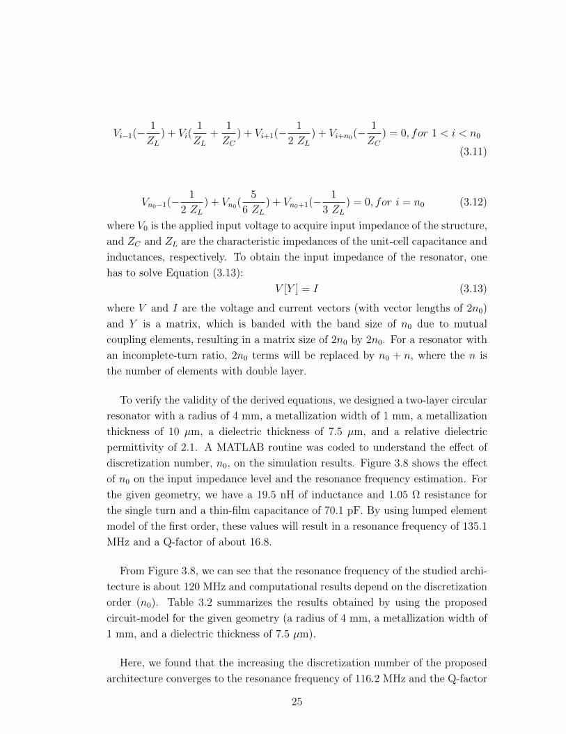
To verify the validity of the derived equations, we designed a two-layer circular
resonator with a radius of 4 mm, a metallization width of 1 mm, a metallization
thickness of 10 µm, a dielectric thickness of 7.5 µm, and a relative dielectric
permittivity of 2.1. A MATLAB routine was coded to understand the effect of
discretization number, n0, on the simulation results. Figure 3.8 shows the effect
of n0 on the input impedance level and the resonance frequency estimation. For
the given geometry, we have a 19.5 nH of inductance and 1.05 Ω resistance for
the single turn and a thin-film capacitance of 70.1 pF. By using lumped element
model of the first order, these values will result in a resonance frequency of 135.1
MHz and a Q-factor of about 16.8.
From Figure 3.8, we can see that the resonance frequency of the studied archi-
tecture is about 120 MHz and computational results depend on the discretization
order (n0). Table 3.2 summarizes the results obtained by using the proposed
circuit-model for the given geometry (a radius of 4 mm, a metallization width of
1 mm, and a dielectric thickness of 7.5 µm).
Here, we found that the increasing the discretization number of the proposed
architecture converges to the resonance frequency of 116.2 MHz and the Q-factor
25

Figure 3.8: Real part of the input impedance for the double-layer helical res-onator.
Table 3.2: Numerical results of the proposed equivalent circuit method for double-layer helical resonator using different discretization order (n0).
n0 Resonance Frequency f3dB Q-factor Computation Time(MHz) (MHz) (s)
2 110.2 2.6 42.4 0.0195 115.4 2.4 48.1 0.06910 116.0 2.5 46.4 0.128100 116.2 2.6 44.7 4.8200 116.2 2.6 44.7 25.6
of about 44.7. We also observed that using conventional equations of resonance
frequency (Equation (3.1)) and Q-factor (Equation (3.2)), do not yield correct
results due to the nature of the proposed architecture. Since we have a thin-
film loaded geometry, it will neither behave like a simple series resonator, nor a
parallel resonator. It is more like a cascaded RLC circuit with proper feedback
(in the electrical model, which corresponds to a physical connection called via-
metallization) to provide better resonance behavior in terms of the feasible sets
of resonance frequency and Q-factor. Hence, instead of using a simple RLC
equivalent circuit, the proposed circuit model characterizes the behavior of our
structure more correctly.
In addition to convergent and correct solutions, computation duration of the
proposed equivalent circuit method is very short compared to traditional full-
wave solvers. When we check Table 3.2 carefully, we see that n0=10 could also be
26
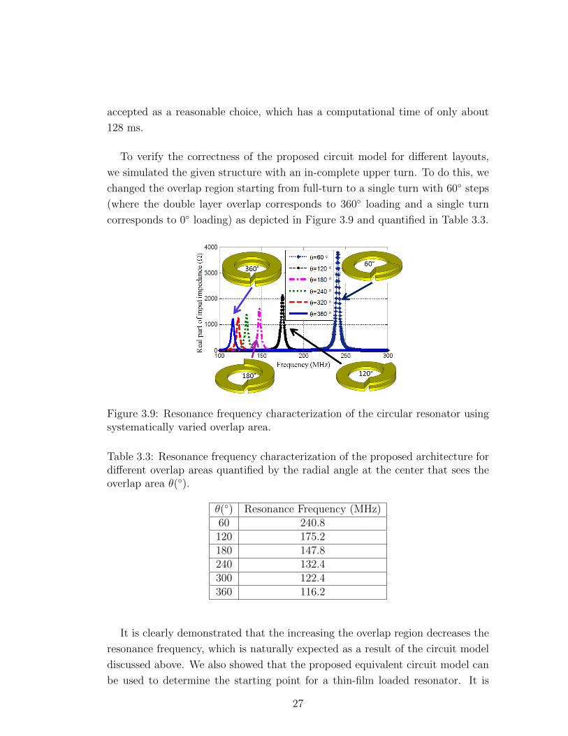
accepted as a reasonable choice, which has a computational time of only about
128 ms.
To verify the correctness of the proposed circuit model for different layouts,
we simulated the given structure with an in-complete upper turn. To do this, we
changed the overlap region starting from full-turn to a single turn with 60 steps
(where the double layer overlap corresponds to 360 loading and a single turn
corresponds to 0 loading) as depicted in Figure 3.9 and quantified in Table 3.3.
Figure 3.9: Resonance frequency characterization of the circular resonator usingsystematically varied overlap area.
Table 3.3: Resonance frequency characterization of the proposed architecture fordifferent overlap areas quantified by the radial angle at the center that sees theoverlap area θ().
θ() Resonance Frequency (MHz)60 240.8120 175.2180 147.8240 132.4300 122.4360 116.2
It is clearly demonstrated that the increasing the overlap region decreases the
resonance frequency, which is naturally expected as a result of the circuit model
discussed above. We also showed that the proposed equivalent circuit model can
be used to determine the starting point for a thin-film loaded resonator. It is
27
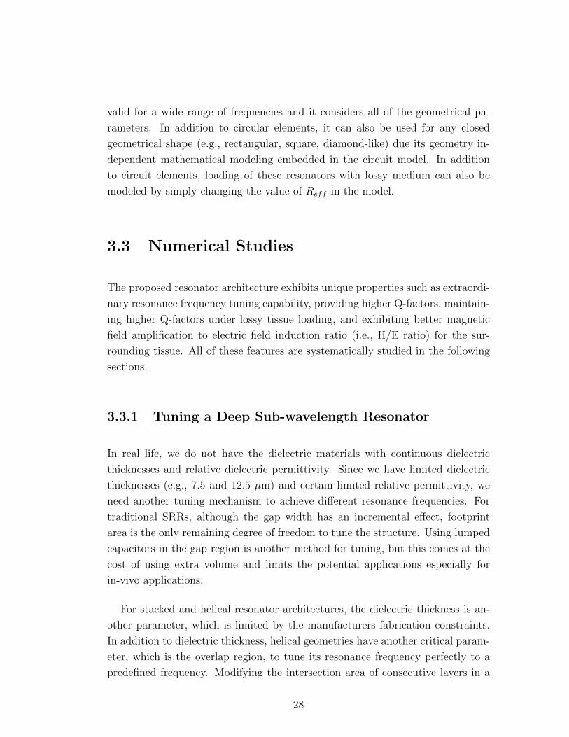
valid for a wide range of frequencies and it considers all of the geometrical pa-
rameters. In addition to circular elements, it can also be used for any closed
geometrical shape (e.g., rectangular, square, diamond-like) due its geometry in-
dependent mathematical modeling embedded in the circuit model. In addition
to circuit elements, loading of these resonators with lossy medium can also be
modeled by simply changing the value of Reff in the model.
3.3 Numerical Studies
The proposed resonator architecture exhibits unique properties such as extraordi-
nary resonance frequency tuning capability, providing higher Q-factors, maintain-
ing higher Q-factors under lossy tissue loading, and exhibiting better magnetic
field amplification to electric field induction ratio (i.e., H/E ratio) for the sur-
rounding tissue. All of these features are systematically studied in the following
sections.
3.3.1 Tuning a Deep Sub-wavelength Resonator
In real life, we do not have the dielectric materials with continuous dielectric
thicknesses and relative dielectric permittivity. Since we have limited dielectric
thicknesses (e.g., 7.5 and 12.5 µm) and certain limited relative permittivity, we
need another tuning mechanism to achieve different resonance frequencies. For
traditional SRRs, although the gap width has an incremental effect, footprint
area is the only remaining degree of freedom to tune the structure. Using lumped
capacitors in the gap region is another method for tuning, but this comes at the
cost of using extra volume and limits the potential applications especially for
in-vivo applications.
For stacked and helical resonator architectures, the dielectric thickness is an-
other parameter, which is limited by the manufacturers fabrication constraints.
In addition to dielectric thickness, helical geometries have another critical param-
eter, which is the overlap region, to tune its resonance frequency perfectly to a
predefined frequency. Modifying the intersection area of consecutive layers in a
28

helical ring allows us to change the thin-film capacitance as well as the mutual
inductance to tune a structure over a wide range of frequencies. This can be
achieved after its manufacturing as well; hence, it is an attractive way of tuning
because of its practicality.
To systematically analyze the effect of overlap area on the resonance frequency,
we used the previously defined rectangular helical resonator with a side length of
8 mm, a gap size of 1 mm, a metallization width of 1 mm, and a metallization
thickness of 10 µm. When a full-turn double-layer helical resonator is manu-
factured, it will have a parallel plate area of 27 mm2. It is expected that this
configuration has the lowest resonance frequency that can be achieved in the given
physical dimensions. Partial removal of one of the layers will result in decreased
thin-film capacitance, as well as decreased effective inductance; hence, a higher
resonance frequency will be observed as shown in Figure 3.10.
Figure 3.10: Frequency characteristics of the proposed resonator design for differ-ent overlapping thin-film regions. It is seen that resonance frequencies of about120 to 450 MHz is achievable by partial removal of the overlay.
According to the obtained results, not only achieving a low resonance frequency
but also tuning this resonance frequency precisely to a predefined value by simply
etching the overlay region is possible. This opens up a wide range of applications
including in-vivo ones.
To broaden our systematic study, we analyzed the resonance frequency of
the provided structures for their different dielectric thicknesses . As mentioned
earlier, provided design has the total thin-film capacitance area of 27 mm2 among
29

consecutive layers for a full turn. This time, we showed the resonance frequency
as a function of percentage ratio of the etched area to the maximum thin-film
area. Figure 3.11 presents the results of this systematic study.
Figure 3.11: Frequency tuning property of the proposed resonator architecturefor different dielectric thicknesses. It is observed that the resonance frequenciesfrom 70 MHz to 5.5 GHz is possible using the given footprint area and varyingdielectric thicknesses.
It is clearly seen that the upper limit for the resonance frequency is about 5.5
GHz, which is independent from the dielectric thickness. This is reasonable due
to the diminishing effect of thin-film capacitance for a single-layer SRR (A %100
percent etch ratio corresponds to complete removal of one of the layers).
From the Figure 3.11, we can observe the effect of dielectric thickness on the
resonance frequency. As the dielectric thickness becomes thinner (decreasing
down to 2.5 µm in this study), thin-film capacitance becomes larger, resulting
in lowered resonance frequencies for all cases. In contrast, increasing dielectric
thickness (increasing to 30 µm in this study) increases the resonance frequency
for all scenarios.
Additionally, there are several possible approaches to reach a predefined res-
onance frequency for the given results. For example, to obtain the resonance
30

frequency of 300 MHz, one can choose a design with a 35% etch ratio and a
dielectric thickness of 30 µm or a 95% etch ratio with a 2.5 µm dielectric thick-
ness, or any solution in between these two. Practically, this property allows us to
use different materials with different thicknesses to achieve the same resonance
frequency. For example, if you need to have a very-thin resonator, it is better to
choose the thinner dielectrics with higher percentage etch ratio. If the mechanical
issues (bending, twisting or inducing strain on the resonator) force us to use the
thicker dielectrics, then we can choose to use the 30 µm scenario with lower etch
ratio.
3.3.2 Q-factor Analyses
Q-factor is one of the key performance indicators of a resonator. The higher the
Q-factor is, the better it is to accomplish its purpose. As previously defined, Q-
factor of a structure can be increased by increasing its energy storage capability
and decreasing losses due to finite conductivity of metallization and non-zero
resistivity of surrounding medium.
To systematically analyze the Q-factor of the proposed resonator design, we
started with an arbitrary resonance frequency of 250 MHz, which can be achieved
by using the dielectric thicknesses given in the previous section. We tuned the
given resonator architecture to this resonance frequency for different dielectric
thicknesses. Q-factor of the overall system is calculated by using Equation (3.14):
Quality Factor = 2πEnergy Stored in the Simulation Domain
Total Power Dissipiated in One Period(3.14)
Here the Power Density and Energy Density monitors with the Time Domain
Solver of the CST Microwave Studio are used for necessary calculations. The
geometrical parameters are reported in Table 3.4 to achieve the same frequency.
Figure 3.12 depicts the parameters provided in Table 3.4.
These two graphs given in Figure 3.12 are exactly the same and acquired from
Table 3.4. Here, we see that the Q-factor of the given resonator is increasing due
to increased overlay region and also due to the thickness of the dielectric region.
31

Table 3.4: Q-factors of different designs for an arbitrary resonance frequency of250 MHz.
Dielectric Thickness (µm) Ovrelaid Area (mm2) Q-factor2.5 2.4 1075 4.3 155
7.5 6 18010 7.8 19120 15 20930 22 217
Figure 3.12: Q-factors of different designs for an arbitrary resonance frequencyof 250 MHz. (a) Q-factor increases due to increased overlay region. (b) Q-factorincreases due to increased dielectric thickness.
As previously explained, increasing overlay region, in other words the turn ratio,
increases the effective inductance given the footprint area and results in the in-
creased Q-factor [55]. Similarly, increasing dielectric thickness also decreases the
capacitance value per unit length, which requires increased inductance to sus-
tain the predetermined resonance frequency. Thus, the Q-factor of the resonator
increases proportional to the overlay area. Additionally, we observed that the
Q-factor seems to asymptotically converge to a value, which we should interpret
using physical explanations.
This issue was previously reported for the conventional structures that their Q-
factor does not increase linearly with their turn ratio due to decreased inductive
coupling between different turns [39]. Although this limitation is not valid for our
design, Figure 3.12 misleads us to draw the correct conclusion (whereas cascaded
32

equivalent circuit model dictates linear relationship between the Q-factor and the
number of turns). The main reason for these results is the improper choice of
calculation domain. In literature, as well as in our method, simulation domain is
filled with free space that is lossless. For thinner dielectric regions, total loss is
small compared to thicker dielectrics. Hence, although it is not fair, the overall
dissipated power increases due to increased dielectric thickness. This seems a
limitation and causes saturation in the Q-factor calculations.
As an ultimate example, let us fill a large simulation domain using a lossy
dielectric (with a loss-tangent of δ) that contains a small resonator and a plane
wave excitation for the calculation. The plane wave solution in this medium (with
negligible resonator effect) will have an effective Q-factor of about 1/tan(δ). For
our case, polyimide film used in the simulations has a loss tangent of 0.003, which
results in the Q-factor of about 330.
Figure 3.13: Schematics of the calculation domain at the resonance frequencyof 250 MHz for different design parameters (not drawn to scale). (a) A thin-film region thickness of 30 µm with a 95% of overlay area, (b) a thin-film regionthickness of 20 µm with a 63% of overlay area, and (c) a thin-film region thicknessof 10 µm with a 33% of overlay area.
To make a fair comparison among different design parameters we determined a
constant volume (a volume that contains the whole resonator) for energy storage
and power dissipation calculations. To do this, we set a region with a thickness
of 100 µm to include the whole design and limited our calculation medium to this
volume (including the dielectric and resistive losses) to eliminate the contribution
of enlarging dielectrics. The overall structures are sketched in Figure 3.13. By
considering field distributions only in the given dielectric volume, we obtained
the curves for Q-factors as reported in Figure 3.14.
Here we see that the overall Q-factor is decreased from about 200 to 20 for 10
µm thin-film layer thickness. This is absolutely in agreement with the expected
33
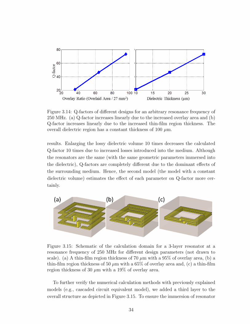
Figure 3.14: Q-factors of different designs for an arbitrary resonance frequency of250 MHz. (a) Q-factor increases linearly due to the increased overlay area and (b)Q-factor increases linearly due to the increased thin-film region thickness. Theoverall dielectric region has a constant thickness of 100 µm.
results. Enlarging the lossy dielectric volume 10 times decreases the calculated
Q-factor 10 times due to increased losses introduced into the medium. Although
the resonators are the same (with the same geometric parameters immersed into
the dielectric), Q-factors are completely different due to the dominant effects of
the surrounding medium. Hence, the second model (the model with a constant
dielectric volume) estimates the effect of each parameter on Q-factor more cer-
tainly.
Figure 3.15: Schematic of the calculation domain for a 3-layer resonator at aresonance frequency of 250 MHz for different design parameters (not drawn toscale). (a) A thin-film region thickness of 70 µm with a 95% of overlay area, (b) athin-film region thickness of 50 µm with a 65% of overlay area and, (c) a thin-filmregion thickness of 30 µm with a 19% of overlay area.
To further verify the numerical calculation methods with previously explained
models (e.g., cascaded circuit equivalent model), we added a third layer to the
overall structure as depicted in Figure 3.15. To ensure the immersion of resonator
34

into the given dielectric, we changed its thickness from 100 to 250 µm. We again
tuned the above structure to an arbitrary frequency of 250 MHz for all scenarios
to eliminate the effect of resonance frequency on the Q-factor calculation. From
Figure 3.16, it is observed that the Q-factor of the proposed resonator increases
almost linearly for the given turn number with a similar slope for each turn. This
allows us to draw a conclusion of increasing Q-factor with an increasing turn ratio
(Q ∝ n) due to the increase in mutual inductance among different layers.
Figure 3.16: Q-factors of different designs for an arbitrary resonance frequency.Q-factor increases linearly due to increased turn ratio as expected from cascaded-equivalent-circuit models.
In conclusion, we successfully modeled the proposed resonator architecture
using full-wave numerical solutions to estimate its Q-factor. The trends found in
these numerical studies are in agreement with our previously reported cascaded-
equivalent-circuit models.
3.3.3 Loading Effect
Designing a conventional resonator for a free-space application is straightforward
and several methods can be used for it. However, using a resonator in living tis-
sues requires special features including maintaining the Q-factor and low electric
field deposition in the surrounding medium. All of these parameters are more
or less related to each other and the physical interpretation to this can be given
usgin the notion of electric field confinement. Although the free-space Q-factor of
35

a resonator can be increased by using conventional methods, maintaining high Q-
factors in a lossy environment requires novel designs. The most important factor
affecting the Q-factor is the electrical losses caused by the resonators. For a given
inductance, which determines the stored inductive energy, a design with a strong
electric field confinement outside the resonator volume will be more vulnerable
to loading [56].
Electric field distribution of conventional structures (including SRRs, spirals
etc.) protrudes from their plane that makes them prone to loading. The proposed
double-layer thin-film geometry has the advantage of electric field confinement in
the low-loss dielectric region that allows for higher Q-factor and lower resonance
frequency shifting. To analyze the superiority of the proposed architecture, we
numerically evaluated its electric field confinement property. Figure 3.17 depicts
the normalized electric field distribution at the resonance frequency of the archi-
tecture.
Figure 3.17: Electric field confinement property of the proposed resonator archi-tecture. (a) Amplitude of the electric field normalized to incident field along withthe dashed line marked in (b) shows that the electric field is 6 orders of magnitudehigher in the localized region on resonance with respect to the incident field.
Figure 3.17(a) presents the normalized electric field profile along with the
dashed line marked in Figure 3.17(b). Here, it is observed that the electric field
is 6 orders of magnitude higher in the dielectric region compared to the incident
field and about 3 orders of magnitude higher compared to off-resonance case.
From Figure 3.17(b), it is clearly observed that the electric field distribution is
strongly localized in the dielectric region between the top and bottom metallic
layers, which is essential to achieving high Q-factor even when loaded with a lossy
medium including biological tissues.
36

The proposed resonator structure exhibits unique properties for wireless oper-
ation that are critical to in-vivo studies. Conventional designs, e.g., single and
stacked SRR without a cross-via metallization, have lowered electric field con-
finement and isolation in the insulator region. On the other hand, the proposed
device properly confines the electric field inside its dielectric material between
its metallic layers to increase the energy storage volume. Thus, this allows us to
store more energy resulting in the increased Q-factor. Additionally, living tissues
exhibit higher conductive losses, e.g., conductivity of 1 S/m, whereas the dielec-
tric losses are radically lower, e.g., conductivity of 10−16 S/m for Kapton. Hence,
confining electric field inside the dielectric substrate, instead of living tissues,
drastically decreases the dissipated resistive power at the given frequency when
this structure is placed in a lossy media. Thus, this helps to keep up the Q-factor
of the proposed resonator significantly higher also when loaded in-vivo.
To make a comparison with a conventional SRR geometry, we numerically
calculated the electric field distribution of the both structures along with the
dielectric region used for metal deposition. Figure 3.18 depicts the comparison
between the proposed structure (a) and the conventional SRR (b) for the same
resonance frequency. The given SRR is loaded with a lumped capacitor of 30
pF from its gap region to achieve this resonance frequency, whereas the proposed
architecture is self-resonant for the previously given layout parameters.
Figure 3.18: Electric field confinement comparison of the proposed architecture(a) and the conventional SRR (b). Conventional SRR is loaded with a capacitorof 30 pF to achieve the same resonance frequency. Electric field confinementof the proposed structure is more than two orders-of -magnitude (2 × 10⁶/104)higher than the conventional SRRs.
Here, it is seen that the electric field distribution of the proposed structure
37

reaches about 2×10⁶ V/m (with the exact value calculated as 2.13×10⁶ V/m)
where the conventional SRR has only the electric field value of about 104 V/m
(with the exact value calculated as 10,970 V/m). Here, over two-orders-of-
magnitude difference in electric field confinement is observed, which is a strong
indicator of high Q-factor under lossy medium loading.
In addition to the electric field confinement property of the proposed structure
outperforming the conventional SRRs, it is also not to spill its confined electric
field over the surrounding medium. Figure 3.19 is provided to depict this property
qualitatively. The proposed structure (Figure 3.19(a)) does not spill over its
electric field into the medium, whereas the conventional SRR (Figure 3.19 (b))
has a wider electric field distribution across the outer plane. This is maximized in
its gap region due to convection currents of the gap capacitor, which is expected
to cause more interaction between the resonator and the surrounding medium.
Figure 3.19: Electric field spill-over comparison between the proposed architec-ture (a) and the conventional SRR (b).
This is also quantified in Figure 3.20 that the proposed structure strongly
confines its electric field in the dielectric region (almost two orders of magnitude
better confinement in e-field distribution) without causing any magnetic field
degradation (left). Magnetic field distribution of a conventional resonator along
with a fictitious curve passing through its geometric center is depicted by a blue
dashed curve and the magnetic field distribution of the proposed architecture
along with a fictitious curve passing through its geometric center is depicted by a
green dotted curve (both in plots and schematic (Figure 3.20-Left). It is seen that
the magnetic field distributions are similar. Similarly, Electric field distribution
of a conventional resonator along with a fictitious curve passing through its split
region is depicted by a blue dashed curve and the electric field distribution of the
proposed architecture along with fictitious curves passing through its metal traces
38
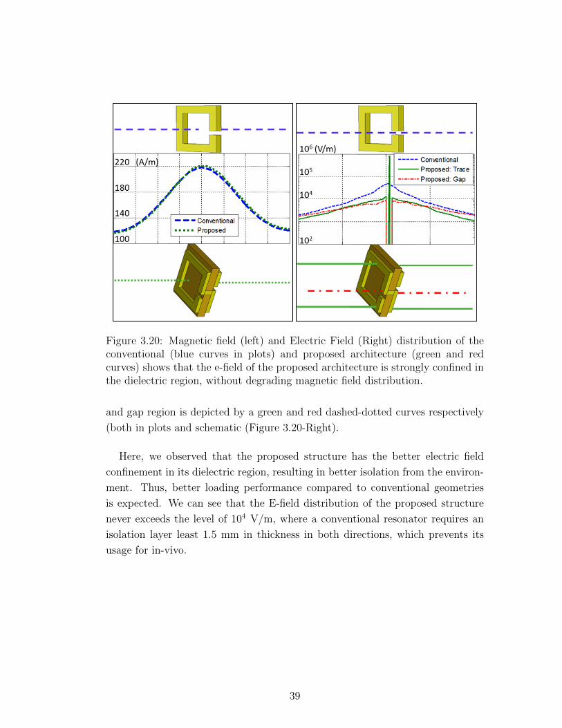
Figure 3.20: Magnetic field (left) and Electric Field (Right) distribution of theconventional (blue curves in plots) and proposed architecture (green and redcurves) shows that the e-field of the proposed architecture is strongly confined inthe dielectric region, without degrading magnetic field distribution.
and gap region is depicted by a green and red dashed-dotted curves respectively
(both in plots and schematic (Figure 3.20-Right).
Here, we observed that the proposed structure has the better electric field
confinement in its dielectric region, resulting in better isolation from the environ-
ment. Thus, better loading performance compared to conventional geometries
is expected. We can see that the E-field distribution of the proposed structure
never exceeds the level of 104 V/m, where a conventional resonator requires an
isolation layer least 1.5 mm in thickness in both directions, which prevents its
usage for in-vivo.
39

3.3.4 E- and H-Field Distributions
Electric field confinement of a resonator shows its energy storage capability and
isolation of this region from the environment implies a better protected perfor-
mance under loading in terms of resistive losses (hence, leading to higher Q-
factors) for the given structure. Although E-field isolation can be achieved by
using non-conducting coatings, magnetic field distribution of the resonator comes
into the picture especially for MRI applications. Not only confining electric field,
but also the amplification of magnetic field in the vicinity of a structure is critical
to make it useful for MRI applications such as marking [46].
Figure 3.21 depicts the electric field and magnetic field distributions of the
proposed resonator structure with the previously defined geometric parameters.
Here, it is seen that the electric field distribution of the proposed structure maxi-
mizes at about 2×10⁶ V/m (while the exact value is calculated as 2.13×10⁶ V/m)
and the magnetic field, at about 1.5×10³ V/m (while the exact value is calculated
as 1,497 A/m). The best point for these two field distributions is the location
of their maxima. The maximum of the electric field is located in the dielectric
thin film, which is important to isolate the structure from loading effect of the
environment and also isolating the environment from the heating effect of the
structure. Similarly, the maximum of the magnetic field is located outside this
dielectric thin-film that is important for magnetic resonance imaging.
Figure 3.21: Field Distributions: Electric field (a), and magnetic field (b) distri-bution of the proposed architecture.
To visualize the superiority of the proposed resonator in terms of the electric
fields for better understanding and quantify the relationship, we calculated the
ratio of magnetic field to electric field values on the same plane as depicted in
40
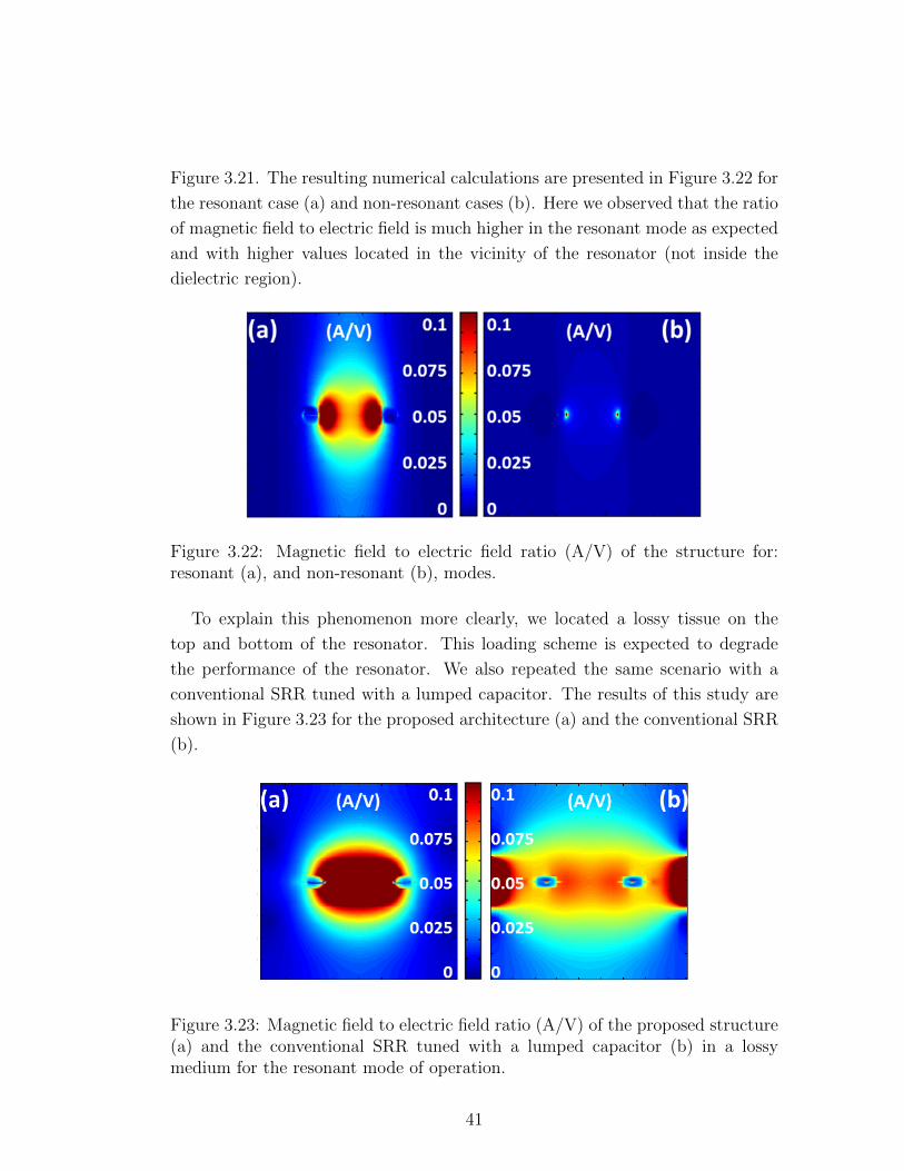
Figure 3.21. The resulting numerical calculations are presented in Figure 3.22 for
the resonant case (a) and non-resonant cases (b). Here we observed that the ratio
of magnetic field to electric field is much higher in the resonant mode as expected
and with higher values located in the vicinity of the resonator (not inside the
dielectric region).
Figure 3.22: Magnetic field to electric field ratio (A/V) of the structure for:resonant (a), and non-resonant (b), modes.
To explain this phenomenon more clearly, we located a lossy tissue on the
top and bottom of the resonator. This loading scheme is expected to degrade
the performance of the resonator. We also repeated the same scenario with a
conventional SRR tuned with a lumped capacitor. The results of this study are
shown in Figure 3.23 for the proposed architecture (a) and the conventional SRR
(b).
Figure 3.23: Magnetic field to electric field ratio (A/V) of the proposed structure(a) and the conventional SRR tuned with a lumped capacitor (b) in a lossymedium for the resonant mode of operation.
41

Here, it is seen that the loading of the proposed architecture does not de-
grade its performance unlike in the conventional SRR and its H/E distribution
ratio is more suitable for MRI applications. From these results, different than
conventional structures (including SRRs), we can foresee that the proposed ar-
chitecture should be operating with little degradation of performance for the
in-vivo applications. For example, its Q-factor performance is expected not to
degrade significantly due to loading with a lossy tissue. Additionally, since the
electric field is confined inside the dielectric region, in the case of using the pro-
posed resonator, we expect comparably lower temperature increases and specific
absorption rates (SAR) for the surrounding medium (compared to conventional
resonators architectures).
3.4 Microfabrication
Although different microfabrication methods for micro-ring resonators have been
proposed previously [57], the fabrication methodology of the proposed resonator
architecture here is carefully designed for high yields for mass production and
lower treatment with chemicals to preserve biocompatibility. A process flow for
microfabrication methodology on a rigid silicon substrate is illustrated in Figure
3.24.
A positive photoresist (AZ 5214, AZ-Microchemicals) was spin coated onto a
Si substrate, followed by ultraviolet (UV) lithography to create features for the
bottom layer of the resonator. A thermal evaporation method was used to deposit
the titanium/gold (Ti/Au) metals and lift-off was applied by using acetone with
1 minute of immersion. At the end of these processes, we obtained conventional
SRR geometry fabricated on a Si substrate with the previously given footprint
area.
To make the capacitive regions, we deposited the silicon-nitride (Si3N4)
onto the whole substrate by using plasma-enhanced chemical vapor deposition
(PECVD) method. The dielectric was then chemically etched to construct the
cross-via metallization by using diluted hydrofluoric acid (HF) solution (about
1% of HF solution).
42

Figure 3.24: Schematic illustration for the microfabrication of the proposed res-onator architecture onto a rigid silicon substrate by using conventional methods.
43
Subsequent fabrication of the second layer was almost the same as the first
one, with proper alignment. Here, the alignment accuracy determines the pre-
cision of targeting a resonance frequency and potential mismatches between the
numerical calculations and the experimental results will stem from this second
layer deposition. After the fabrication of the second layer, Si wafer was rinsed
and dried followed by a 5 min rapid thermal annealing at 250 C.
Although the proposed microfabrication methodology may be suitable for mass
production, it is not preferred due to potential biocompatibility issues. Using
photoresist for in-vivo device fabrication might render dangerous as the remnants
of the HF could be fatal for in-vivo applications.
Using UV photolithography allows us to create features as small as 1 µm with
almost the same alignment accuracy. This level of accuracy is very critical to
fabricate a device with predetermined parameters especially for the structures
without a tuning capability. However, the proposed resonator design is capable
of wide range of resonance frequency tuning. Thus, we can use relatively rough
methods to fabricate the metallization layers and cross-via connection that would
make the fabrication more cost effective and biocompatible.
Here, a new process flow to fabricate the proposed structure is designed by us-
ing hard masks (also known as shadow masks) with complementary SRR shapes.
Using a hard mask prevents us to achieve a µm-level precision, which is not a limi-
tation for our structure, but simplifies the fabrication steps significantly. The new
microfabrication methodology to create the proposed architecture is illustrated
in Figure 3.25.
A shadow mask with asymmetric comb sized SRR shapes was manually placed
on top of a substrate to allow for Ti/Au vapor to penetrate through the open
regions and create SRR shapes. By this method, the usage of UV illumination
can be omitted at a cost of lowered fabrication accuracy. Dielectric coating and
etching were than undertaken by using the same PECVD methodology as de-
scribed earlier. The second layer and the cross-via metallization were coated by
using the same hard mask with complementary side to allow for the creation of
the helical geometry.
This simplified proces flow does not include any photoresist coating and UV
44

Figure 3.25: Schematic illustration for the microfabrication of the proposed res-onator architecture onto a rigid silicon substrate by using simplified methods.
lithography methods, which makes it potentially safer compared to conventional
techniques. Additionally, decreasing the number of steps allows us to increase
the fabrication yield, which makes this process flow more promising for practical
applications. Figure 3.26 shows the optical photography of the microfabricated
samples with different footprint areas onto a rigid substrate by using the simplified
approach.
Fabrication of the proposed helical architecture onto a flexible substrate can
also be achieved by using the same process flow as described above. This time,
one should be more careful to handle the overall sheet of flexible substrate and
alignment of the hard mask will be more difficult. Hence, this alignment problem
will lead to large discrepancies for the resonance frequency between the numerical
solutions and the experimental results. Similarly, replacing a rigid substrate with
a flexible one, one ends up having two layers of dielectric (one is for the substrate
and the other one for the dielectric region) and in principle one of these could
serve the purpose of the other. Hence, at this point our idea was to use a substrate
45

Figure 3.26: Optical photograph of the microfabricated samples on rigid sub-strate by using simplified methods. The ease of fabrication comes at the costof misalignment that would result in increased resonance frequency discrepanciesbetween the numerical and experimental results.
as a dielectric region and to make an ultra-thin helical structure.
Using a flexible substrate, which also serves as a dielectric region, eliminates the
nitride deposition step and further simplifies the microfabrication methodology to
increase yield and biocompatibility. The process flow to create helical structures
using both sides of a polyimide film is illustrated in Figure 3.27.
Here, a shadow mask including complementary SRR shapes with asymmetric
comb sizes was used to deposit a layer of patterns on one side of the polyimide
tape. Then, the tape was turned upside down to coat the second layer and cross-
via metallization. Unlike the conventional HF-based etching of silicon nitride,
the polyimide was etched by using mechanical drilling. The second layer of met-
allization was deposited by using the same hard mask. In the end, the polyimide
substrate was sandwiched between two metallization layers so that it was used
as a capacitive region between the metal levels. This decreases the device thick-
ness significantly, leading to ultra-thin and flexible self-resonant device [47]. The
optical photographs of the fabricated samples are provided in Figure 3.28 for the
side lengths of 14 mm (a) and 8 mm (b).
46

Figure 3.27: Schematic representation for the microfabrication of the proposedarchitecture onto a flexible substrate by using simplified methods.
Figure 3.28: Optical photographs of the microfabricated samples on flexible poly-imide thin-films by using simplified methods for (a) 14 mm and (b) 8 mm sidelengths.
3.5 RF Characterization
Characterization of a wireless circuit component is different than its wired coun-
terparts. Measuring scattering parameters (S11, S21, etc.) clearly defines the
operation of wired circuit elements such as waveguides, transmission lines, induc-
tors, and resonators. However, characterization of a wireless structure requires
designing specific measurements and modeling techniques to determine its char-
acteristic parameters.
As described in Section 3.2, our proposed thin-film loaded helical structure
can be modeled by its cascaded equivalent circuit to determine its characteristic
parameters including the resonance frequency and the Q-factor. For numerical
environments, determining a measurement result without touching or changing it,
47
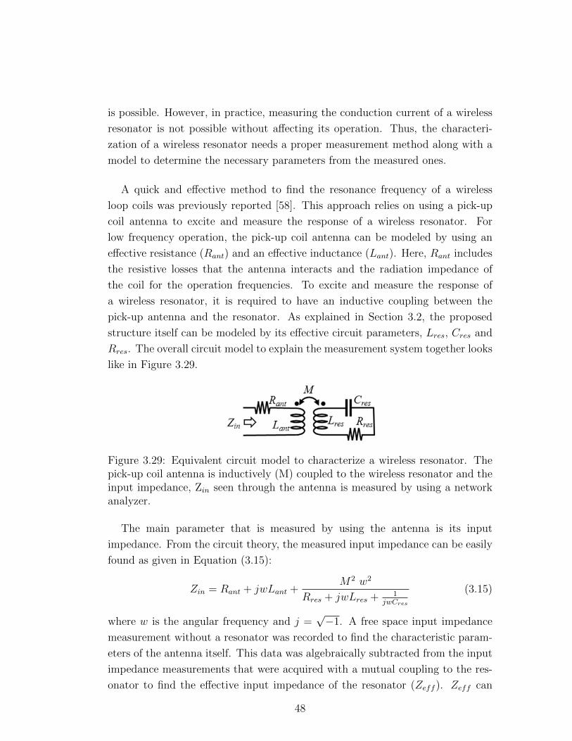
is possible. However, in practice, measuring the conduction current of a wireless
resonator is not possible without affecting its operation. Thus, the characteri-
zation of a wireless resonator needs a proper measurement method along with a
model to determine the necessary parameters from the measured ones.
A quick and effective method to find the resonance frequency of a wireless
loop coils was previously reported [58]. This approach relies on using a pick-up
coil antenna to excite and measure the response of a wireless resonator. For
low frequency operation, the pick-up coil antenna can be modeled by using an
effective resistance (Rant) and an effective inductance (Lant). Here, Rant includes
the resistive losses that the antenna interacts and the radiation impedance of
the coil for the operation frequencies. To excite and measure the response of
a wireless resonator, it is required to have an inductive coupling between the
pick-up antenna and the resonator. As explained in Section 3.2, the proposed
structure itself can be modeled by its effective circuit parameters, Lres, Cres and
Rres. The overall circuit model to explain the measurement system together looks
like in Figure 3.29.
Figure 3.29: Equivalent circuit model to characterize a wireless resonator. Thepick-up coil antenna is inductively (M) coupled to the wireless resonator and theinput impedance, Zin seen through the antenna is measured by using a networkanalyzer.
The main parameter that is measured by using the antenna is its input
impedance. From the circuit theory, the measured input impedance can be easily
found as given in Equation (3.15):
Zin = Rant + jwLant +M2 w2
Rres + jwLres + 1jwCres
(3.15)
where w is the angular frequency and j =√−1. A free space input impedance
measurement without a resonator was recorded to find the characteristic param-
eters of the antenna itself. This data was algebraically subtracted from the input
impedance measurements that were acquired with a mutual coupling to the res-
onator to find the effective input impedance of the resonator (Zeff ). Zeff can
48
then be formulated as given in Equation (3.16):
Zeff =M2 w2
Rres + jwLres + 1jwCres
(3.16)
Having a higher Q-factor ensures the higher input impedance for the real part
of Zeff at the resonance frequency. Similarly, the imaginary part of Zeff is
expected to be zero at the resonance frequency. However, S11 might not have a dip
at the resonance frequency. Hence, tracking the zero crossing for the imaginary
part of Zeff is the most reliable method to determine the resonance frequency.
Similarly, measuring the dip of S11 does not give a reliable result to estimate
the value of Q-factor. Higher Q-factors may result in lowered dips or vice-versa.
Hence, instead of using the curve of S11, we chose to use the complex impedance
values to fit the best curve using equivalent circuit model to estimate its Q-factor
from the effective parameters of Reff , Leff and Ceff based on the formula (3.2).
Figure 3.30 shows the characteristic curves seen through the pick-up antenna
for a resonator with a Leff of 20 nH, a Ceff of 100 pF, a M of 20 nH and Reff
ranging from 1 to 10 Ω. These parameters result in a resonance frequency of
about 112.54 MHz with a Q-factor ranging from 14 to 1.4. This figure proves
the arguments above that the Q-factor of a wireless resonator cannot be deduced
from the tracking of S11 measurement. This task requires proper modeling of
mutual coupling and resonator.
Numerical studies reported in Section 3.3 indicate that a resonance frequency
of about 100 MHz is achievable for the footprint area of 8 mm × 8 mm with a
dielectric thickness of about 10 µm. To achieve the given resonance frequency with
standard polyimide thin-films (e.g., Kapton HN30 has a thickness of 7.5 µm and
Kapton HN50 has a thickness of 12.5 µm), we microfabricated the devices with
14 mm × 14 mm footprint area by using HN50 polyimide thin-film. Resulting
Zeff curves are given in Figure 3.31 for their real parts in (a) and imaginary parts
in (b) separately.
It is clearly seen that the eight samples (out of nine) were microfabricated suc-
cessfully to resonate below 100 MHz, while six of them (Samples 2, 3, 4, 7, 8, and
9) had almost the same characteristic parameters and two of them (Samples 1
49
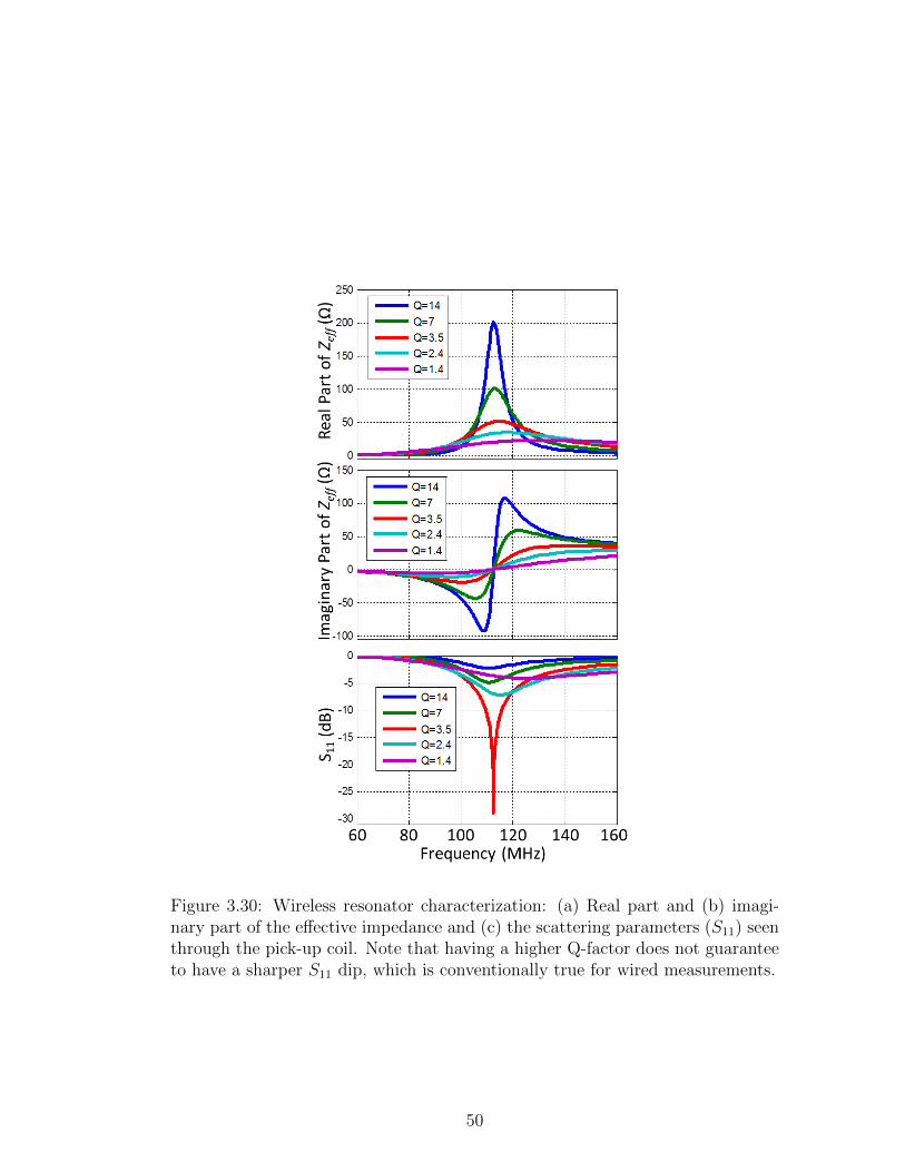
Figure 3.30: Wireless resonator characterization: (a) Real part and (b) imagi-nary part of the effective impedance and (c) the scattering parameters (S11) seenthrough the pick-up coil. Note that having a higher Q-factor does not guaranteeto have a sharper S11 dip, which is conventionally true for wired measurements.
50
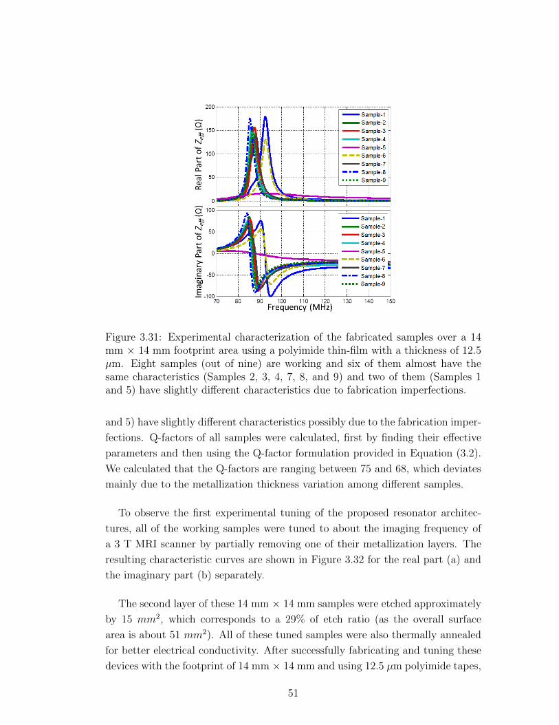
Figure 3.31: Experimental characterization of the fabricated samples over a 14mm × 14 mm footprint area using a polyimide thin-film with a thickness of 12.5µm. Eight samples (out of nine) are working and six of them almost have thesame characteristics (Samples 2, 3, 4, 7, 8, and 9) and two of them (Samples 1and 5) have slightly different characteristics due to fabrication imperfections.
and 5) have slightly different characteristics possibly due to the fabrication imper-
fections. Q-factors of all samples were calculated, first by finding their effective
parameters and then using the Q-factor formulation provided in Equation (3.2).
We calculated that the Q-factors are ranging between 75 and 68, which deviates
mainly due to the metallization thickness variation among different samples.
To observe the first experimental tuning of the proposed resonator architec-
tures, all of the working samples were tuned to about the imaging frequency of
a 3 T MRI scanner by partially removing one of their metallization layers. The
resulting characteristic curves are shown in Figure 3.32 for the real part (a) and
the imaginary part (b) separately.
The second layer of these 14 mm × 14 mm samples were etched approximately
by 15 mm2, which corresponds to a 29% of etch ratio (as the overall surface
area is about 51 mm2). All of these tuned samples were also thermally annealed
for better electrical conductivity. After successfully fabricating and tuning these
devices with the footprint of 14 mm × 14 mm and using 12.5 µm polyimide tapes,
51
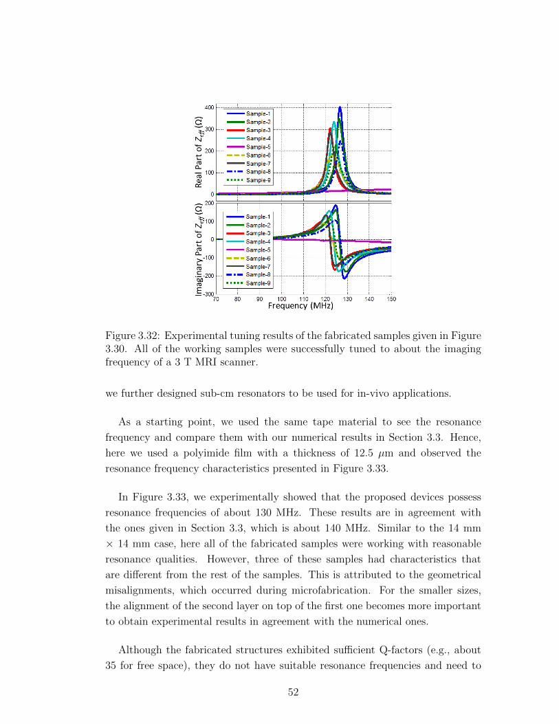
Figure 3.32: Experimental tuning results of the fabricated samples given in Figure3.30. All of the working samples were successfully tuned to about the imagingfrequency of a 3 T MRI scanner.
we further designed sub-cm resonators to be used for in-vivo applications.
As a starting point, we used the same tape material to see the resonance
frequency and compare them with our numerical results in Section 3.3. Hence,
here we used a polyimide film with a thickness of 12.5 µm and observed the
resonance frequency characteristics presented in Figure 3.33.
In Figure 3.33, we experimentally showed that the proposed devices possess
resonance frequencies of about 130 MHz. These results are in agreement with
the ones given in Section 3.3, which is about 140 MHz. Similar to the 14 mm
× 14 mm case, here all of the fabricated samples were working with reasonable
resonance qualities. However, three of these samples had characteristics that
are different from the rest of the samples. This is attributed to the geometrical
misalignments, which occurred during microfabrication. For the smaller sizes,
the alignment of the second layer on top of the first one becomes more important
to obtain experimental results in agreement with the numerical ones.
Although the fabricated structures exhibited sufficient Q-factors (e.g., about
35 for free space), they do not have suitable resonance frequencies and need to
52

Figure 3.33: Experimental characterization of samples over 8 mm × 8 mm foot-print area using a polyimide film with a thickness of 12.5 µm. Eight samples(out of nine) are working but three of them (Samples 2, 3, and 4) have differentcharacteristics due to the fabrication imperfections.
be tuned a pre-defined MRI frequency (123 MHz for this case). Hence, the given
size and dielectric combination (8 mm side length with a 12.5 µm polyimide film)
is not suitable for 3 T MRI applications.
To achieve the lower resonance frequency with sub-cm footprint dimensions, we
replaced our thin-film dielectric with a thinner one, having a thickness of 7.5 µm.
The resonator with the footprint area of 8 mm × 8 mm we discussed previously
was fabricated and its initial characterization curves areshown in Figure 3.34.
Here, three samples (out of four) were working with reasonable resonance
qualities (i.e., Q-factors of about 35-40). Alignment of the second layer on top
of the first one was achieved and these experimental results were in agreement
with the numerical results reported in Section (3.3). It can be concluded that
the proposed size and dielectric combination (i.e., 8 mm side length with a 7.5
µm polyimide thin-film) is suitable for 3 T MRI applications. Additionally, for
the targeted MRI applications, with the resonance frequency of about 120 MHz,
we tuned these structures by partially removing one of their metallization layers.
53

Figure 3.34: Experimental results of the fabricated samples with 8 mm × 8 mmfootprint area using a polyimide film with a thickness of 7.5 µm. Three samples(out of four) are working with slightly different characteristics due to fabricationimperfections.
Results of the experimental tuning steps are shown in Figure 3.35.
Here, one of the fabricated structures (Sample-3 of the Figure 3.35) has been
tuned to the targeted frequency of about 120 MHz by partially removing one of
its layers. Removal of 20% of the top layer, with a corresponding area of about
5.2 mm2 (as the overall top layer has a surface area of 26 mm2 before removal)
results in perfect tuning to 123 MHz in free space. These experimental results
are in agreement with the numerical results reported in Section 3.3. Similarly the
Q-factors of the proposed structures were increased to about 50 after tuning.
It is observed that the tuning of flexible structures from 100 to 120 MHz results
in the increased Q-factor, which is in agreement with the proposed circuit model
(Q-factor= w Leff/Reff ). On the other hand, it is reported that the Q-factor of
the conventional structures, (e.g., spirals, solenoids and SRRs) does not increase
linearly due to the lowered inductance for the consecutive turns [39]. Hence,
this geometry is very special in terms of its improved Q-factor due to the strong
mutual coupling among consecutive layers and the lowered resonance frequency
for the same footprint area.
54
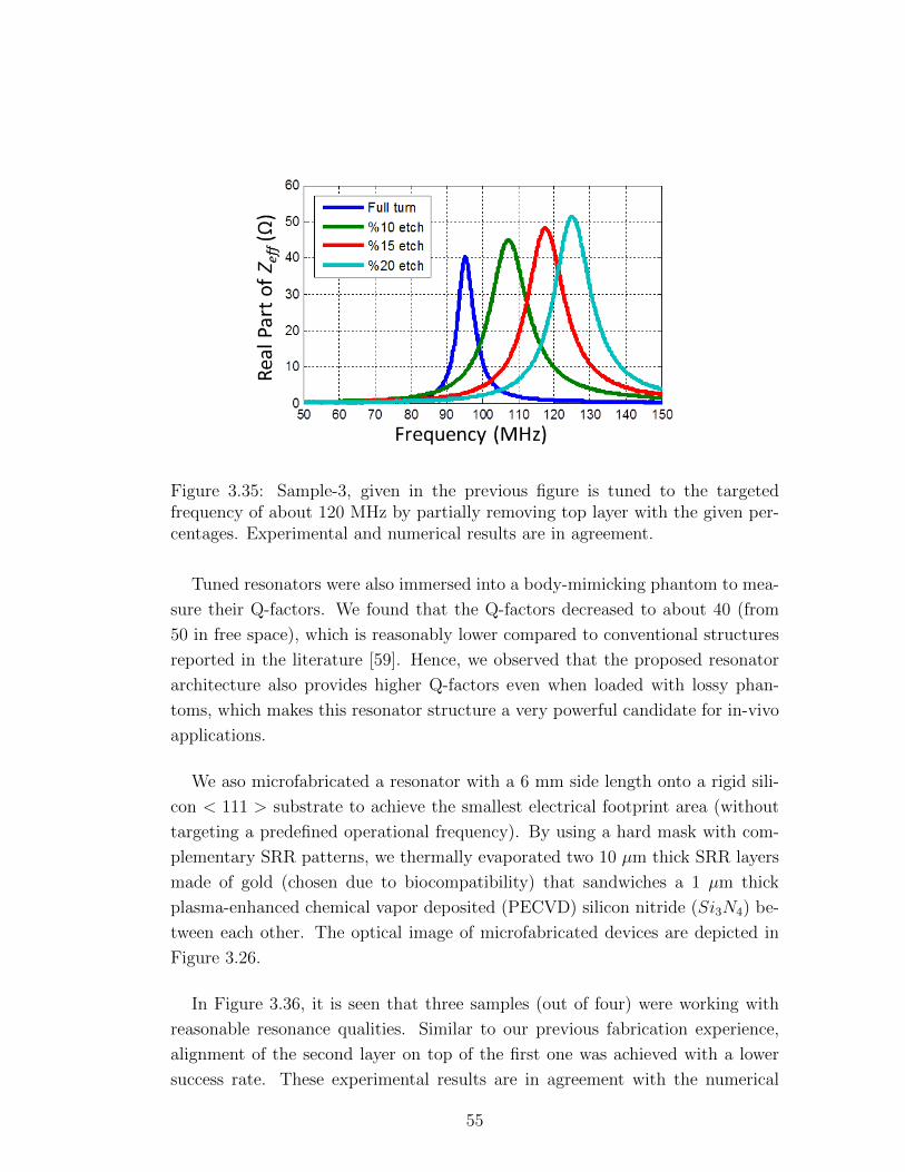
Figure 3.35: Sample-3, given in the previous figure is tuned to the targetedfrequency of about 120 MHz by partially removing top layer with the given per-centages. Experimental and numerical results are in agreement.
Tuned resonators were also immersed into a body-mimicking phantom to mea-
sure their Q-factors. We found that the Q-factors decreased to about 40 (from
50 in free space), which is reasonably lower compared to conventional structures
reported in the literature [59]. Hence, we observed that the proposed resonator
architecture also provides higher Q-factors even when loaded with lossy phan-
toms, which makes this resonator structure a very powerful candidate for in-vivo
applications.
We aso microfabricated a resonator with a 6 mm side length onto a rigid sili-
con < 111 > substrate to achieve the smallest electrical footprint area (without
targeting a predefined operational frequency). By using a hard mask with com-
plementary SRR patterns, we thermally evaporated two 10 µm thick SRR layers
made of gold (chosen due to biocompatibility) that sandwiches a 1 µm thick
plasma-enhanced chemical vapor deposited (PECVD) silicon nitride (Si3N4) be-
tween each other. The optical image of microfabricated devices are depicted in
Figure 3.26.
In Figure 3.36, it is seen that three samples (out of four) were working with
reasonable resonance qualities. Similar to our previous fabrication experience,
alignment of the second layer on top of the first one was achieved with a lower
success rate. These experimental results are in agreement with the numerical
55
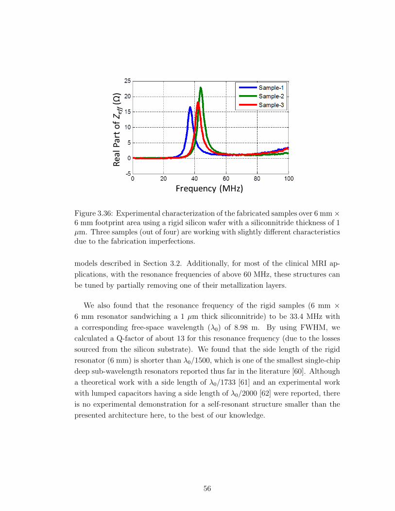
Figure 3.36: Experimental characterization of the fabricated samples over 6 mm×6 mm footprint area using a rigid silicon wafer with a siliconnitride thickness of 1µm. Three samples (out of four) are working with slightly different characteristicsdue to the fabrication imperfections.
models described in Section 3.2. Additionally, for most of the clinical MRI ap-
plications, with the resonance frequencies of above 60 MHz, these structures can
be tuned by partially removing one of their metallization layers.
We also found that the resonance frequency of the rigid samples (6 mm ×6 mm resonator sandwiching a 1 µm thick siliconnitride) to be 33.4 MHz with
a corresponding free-space wavelength (λ0) of 8.98 m. By using FWHM, we
calculated a Q-factor of about 13 for this resonance frequency (due to the losses
sourced from the silicon substrate). We found that the side length of the rigid
resonator (6 mm) is shorter than λ0/1500, which is one of the smallest single-chip
deep sub-wavelength resonators reported thus far in the literature [60]. Although
a theoretical work with a side length of λ0/1733 [61] and an experimental work
with lumped capacitors having a side length of λ0/2000 [62] were reported, there
is no experimental demonstration for a self-resonant structure smaller than the
presented architecture here, to the best of our knowledge.
56
3.6 Metamaterial Characterization
It was previously shown that the full-turn helical structures are a chiral metama-
terials [54] and capacitor-loaded SRRs are also a metastructure [63], but there
has been no study or evidence on the metamaterial characteristic properties of
the partial-turn thin-film loaded resonator architectures. To prove this, we used
CST Microwave Studio to acquire the complex reflection parameters (S11 and
S21). In this simulation environment, we constructed the resonator in the xy
plane with a unitcell boundary conditions in the x and y directions. Simula-
tion ports were located in the z direction with open boundary conditions and
simulation domain was extended over 8 mm in both the positive and negative
z directions. Complex S11 and S21 parameters were exported using the graphi-
cal user interface of the CST Microwave Studio to process with MATLAB. The
acquired scattering parameters were used to retrieve the effective relative permit-
tivity (εr) and permeability (µr) of the metastructure by applying the methods
described elsewhere [64].
To obtain these constitutive parameters, we first calculated the complex re-
flection (Γ) and transmission (T ) coefficients by using the parameter K, as given
in Equations (3.17-3.19):
K =1 + S2
11 − S221
2 S11
(3.17)
Γ = K ±√K2 − 1 = |Γ|ejφ (3.18)
T =S11 + S21 − Γ
1− (S11 + S21)Γ(3.19)
To have a physical meaning, the sign of K was chosen such that the |Γ| < 1,
resulting in the radiation coefficient (γ) given by Equation (3.20):
γ =ln( 1
T)
d+ j
2nπ − φd
for n = 0,±1,±2,±3, ... (3.20)
57

where d is the distance between two waveguide ports. From these propagation
numbers, relative complex permittivity and permeability were calculated as given
in Equations (3.21 and 3.22):
ε∗ =γ
γ0(1− Γ
1 + Γ) (3.21)
µ∗ =γ
γ0(1 + Γ
1− Γ) (3.22)
where γ0 is the complex radiation constant for free space.
Here, we observed that the real parts of the effective permittivity and the
permeability of the proposed metamaterial both exhibit negative values near the
resonance frequency, which does not naturally exist in classical materials.
Figure 3.37: Retrieved material parameters of the tuned resonator for MR imag-ing: (a) the effective relative permittivity, εr, and (b) effective relative permeabil-ity, µr, of this metamaterial architecture have negative values around its resonancefrequency.
We found that the proposed resonator structure with its tuned geometry still
preserves its metamaterial property in terms of its negative constitutive parame-
ters. This is accomplished by properly manipulating EM field within its geometry
58

to have strong resonance characteristics with a high Q-factor. Hence, the pro-
posed resonator architecture is shown to be a tunable metamaterial architecture
with an extraordinary tuning bandwidth and a high Q-factor, suitable for various
applications including in-vivo imaging practices.
59
Chapter 4
MRI with Wireless Resonators
MRI has been attracting increasing interest for the localization of implantable
devices (e.g., subdural electrodes). Although the soft tissue contrast of MRI [1]
makes it the strongest candidate among other imaging modalities (such as X-ray,
CT, and PET), the positioning of devices under MRI requires special treatments
including the use of wired connections [6–11], introducing MRI marker materials
[12–17], and using wireless passive devices with inductive coupling [18,19].
The use of wireless resonant devices is potentially highly promising to mark
implantable devices without requiring multimodal imaging. MRI performance
of these wireless markers is loosely dependent on the imaging parameters (TR,
TE and resolution). However, this requires novel resonator designs for proper
operation. Physical dimensions of these markers together with RF safety concerns
should be considered for the surrounding tissues [20].
In this chapter, we characterized our proposed thin-film resonator architecture
that alleviates the potential complications of the previous works in the literature.
Intensity distribution maps, B1 field distribution, SNR and SAR distribution of
this proposed resonator for various imaging configuration are provided. Exper-
imental temperature studies showed that the proposed devices can be used for
in-vivo applications. This may open up new possibilities for the next-generation
implants that contain their own wireless e-markers integrated on them.
60

4.1 Intensity Distribution Maps
As discussed earlier, MRI signal strength is dependent on the magnetic field
distribution in a tissue. Conventionally, it is mostly accepted that the higher the
signal strength is, the better the signal-to-noise ratio is for a given MR image.
The most primitive method to understand the relative signal quality of a given
MRI image is to characterize its intensity distribution.
MRI measurements were taken using a 3 T Siemens Tim Trio System with
a body-mimicking liquid phantom composed of 2 mM copper sulfide solution
(CuSO4.5H2O, with %98 purity of Merck) and 50 mM of NaCl, which mimics
most of the tissues [65], with a relative permittivity of around 60, conductivity
of 0.5 S/m [66], T1 of 140 ms and T2 of 88 ms. T1 and T2 measurement results
are shown in Figure 4.1.
Figure 4.1: T1 and T2 parameters of the prepared phantom. T1 was measuredto be about 140 ms and T2, to be about 88 ms.
The characteristic parameters of this phantom are suitable to analyze the in-
vivo loading performance of our resonator. Here, initial images were acquired
61

by using a body coil as the transmitter and a standard twelve-channel head coil
as the receiver. We used spoiled gradient echo sequence (also known as the
gradient-recalled echo, GrE), with a 100 mm × 100 mm field of view (FOV)
in the transverse plane, a 256 × 256 image resolution, a 2 mm slice thickness,
TR/TE of 100 ms/10 ms, a 260 Hz pixel bandwidth, a flip angle of 10 and a
total imaging duration of 29 s. Figure 4.2 depicts the intensity distribution of
our resonator with a footprint area of 8 mm × 8 mm.
Figure 4.2: Intensity distribution of the proposed resonator with a footprint areaof 8 mm × 8 mm.
Here we found that the image intensity level, for the applied flip angle of 10,
was amplified from 80 to 1200 for the close vicinity of the resonator. Similarly, at
4 mm away from the resonator, signal intensity was about 600, which is 7.5 times
higher than the original intensity level. Signal intensity drops to about 120 (1.5
times the original intensity level), at a distance 8 mm away from the resonator,
which is also the side length of the resonator itself.
As reported in Figure 4.3, this characterization was extended to different flip
angles for the same imaging parameters as described in Figure 4.2. It is observed
that the signal intensity, within the existence of the resonator, was always higher
than the resonator-free case. But, the intensity amplification of the resonator
was strictly dependent on the imaging angle. This makes the characterization
of the proposed structure difficult. Hence, a more reliable MRI characterization
method, B1 mapping, is needed to give a better explanation for the operating
principle of this resonator.
62

Figure 4.3: Flip-angle characterization of the proposed resonator.
4.2 B1 Mapping of Wireless Resonators
B1 mapping is used in several applications in MRI including T1 mapping [67],
transmit gain adjustment [68–70] and chemical shift imaging. B1 mapping can
be done either by using signal intensity based methods or by using phase based
methods [71]. Intensity based methods strictly depend on the applied RF flip
angle, where the double angle method [72] and fitting progressively increasing
flip angles [73] are two common methods in this category.
These methods suffer from the followings: requirement of large TR to eliminate
T1 effects, higher flip angle to acquire enough signal level (lower flip angles or
180 flip angle cannot be successfully mapped) and higher RF power deposition
for large flip angles or reset pulses to handle T1 dependence. To eliminate these
problems, Bloch-Siegert method is utilized [74].
The relationship between the B1 and flip angle is given in Equation (4.1):
α =
∫ τ
0
γB1(t)dt (4.1)
63
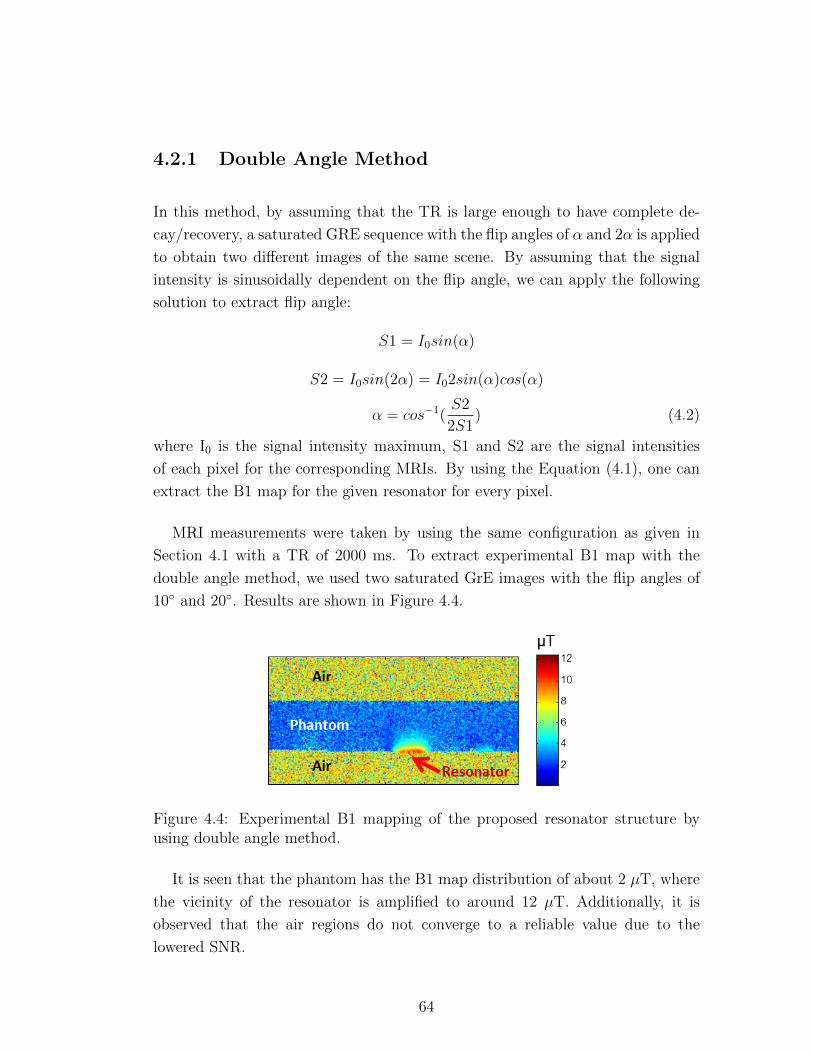
4.2.1 Double Angle Method
In this method, by assuming that the TR is large enough to have complete de-
cay/recovery, a saturated GRE sequence with the flip angles of α and 2α is applied
to obtain two different images of the same scene. By assuming that the signal
intensity is sinusoidally dependent on the flip angle, we can apply the following
solution to extract flip angle:
S1 = I0sin(α)
S2 = I0sin(2α) = I02sin(α)cos(α)
α = cos−1(S2
2S1) (4.2)
where I0 is the signal intensity maximum, S1 and S2 are the signal intensities
of each pixel for the corresponding MRIs. By using the Equation (4.1), one can
extract the B1 map for the given resonator for every pixel.
MRI measurements were taken by using the same configuration as given in
Section 4.1 with a TR of 2000 ms. To extract experimental B1 map with the
double angle method, we used two saturated GrE images with the flip angles of
10 and 20. Results are shown in Figure 4.4.
Figure 4.4: Experimental B1 mapping of the proposed resonator structure byusing double angle method.
It is seen that the phantom has the B1 map distribution of about 2 µT, where
the vicinity of the resonator is amplified to around 12 µT. Additionally, it is
observed that the air regions do not converge to a reliable value due to the
lowered SNR.
64
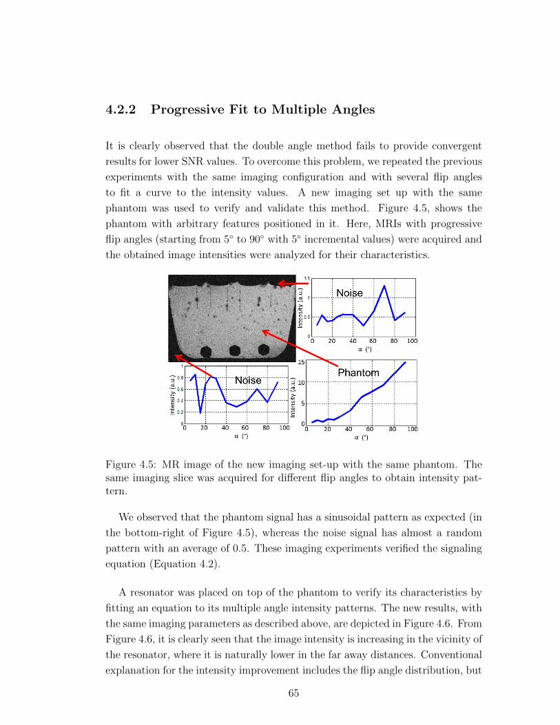
4.2.2 Progressive Fit to Multiple Angles
It is clearly observed that the double angle method fails to provide convergent
results for lower SNR values. To overcome this problem, we repeated the previous
experiments with the same imaging configuration and with several flip angles
to fit a curve to the intensity values. A new imaging set up with the same
phantom was used to verify and validate this method. Figure 4.5, shows the
phantom with arbitrary features positioned in it. Here, MRIs with progressive
flip angles (starting from 5 to 90 with 5 incremental values) were acquired and
the obtained image intensities were analyzed for their characteristics.
Figure 4.5: MR image of the new imaging set-up with the same phantom. Thesame imaging slice was acquired for different flip angles to obtain intensity pat-tern.
We observed that the phantom signal has a sinusoidal pattern as expected (in
the bottom-right of Figure 4.5), whereas the noise signal has almost a random
pattern with an average of 0.5. These imaging experiments verified the signaling
equation (Equation 4.2).
A resonator was placed on top of the phantom to verify its characteristics by
fitting an equation to its multiple angle intensity patterns. The new results, with
the same imaging parameters as described above, are depicted in Figure 4.6. From
Figure 4.6, it is clearly seen that the image intensity is increasing in the vicinity of
the resonator, where it is naturally lower in the far away distances. Conventional
explanation for the intensity improvement includes the flip angle distribution, but
65

this is not enough to explain the behavior in this scenario. If this were the case,
the maximum intensity of all plots should have reach the same value. However,
they are significantly different and the equation of S(α) = I0sin(α) does not
suffice to explain this situation.
Figure 4.6: MRI of the same imaging set-up in the presence of the resonator.Intensity patterns acquired from 1, 2, and 4 mm away from the resonator areplotted to understand its characteristics.
The brightness of certain regions close to the resonator can be seen, which
occurs because of two reasons: the first one is due to the inductive coupling
of transmit-field (B1+ improvement) and the second is due to the receive-field
inductive coupling. Applied RF power induces surface currents proportional to
the resonator Q-factor, which in return creates an effective B1+ field distribution
in its vicinity (B1+Q ∝ Q B1+). The new flip angle (α) distribution will be
proportional to this new B1+Q field distribution (α ∝ γB1+
Q τ , where γ is the
gyromagnetic ratio and τ is the RF signal duration). Hence, the transmit field
contribution to the imaging signal will be proportional to sin(α) ∝ sin(γQB1+τ).
Thus, the image intensity distribution will depend on the Q-factor and the B1+
distribution due to the spatial distribution of this flip angle.
Once the spins are excited in the presence of a resonator, they emit precession
signal that is captured by the resonator and transmitted to the receiver antennas.
This process known as receive-field coupling is a straightforward RF phenomenon,
which is proportional to the Q-factor of the resonator [75]. Hence, the overall
66

Figure 4.7: B1 mapping by using multiple angle method shows that Q-factor ofthe resonator significantly affects the image intensity.
image intensity enhancement profile will be proportional to the multiplication of
these two effects. (SQ=|I0Qsin(Qα)|), here note that Q is position dependent).
The distribution of Q and I0Q is provided in Figure 4.7. We observed that this
method eliminates the effect of noise and resulting in better characterization
results.
Here, a more robust method to obtain the B1 map of a given device is studied.
It is seen that the Q-factor of our resonator is affecting not only the flip angle
distribution but also the reception efficiency of the system due to mutual coupling
between the resonator and the receiver antennas. We observed that the Q-factor
of such a resonator as ours can be estimated by using this method.
67
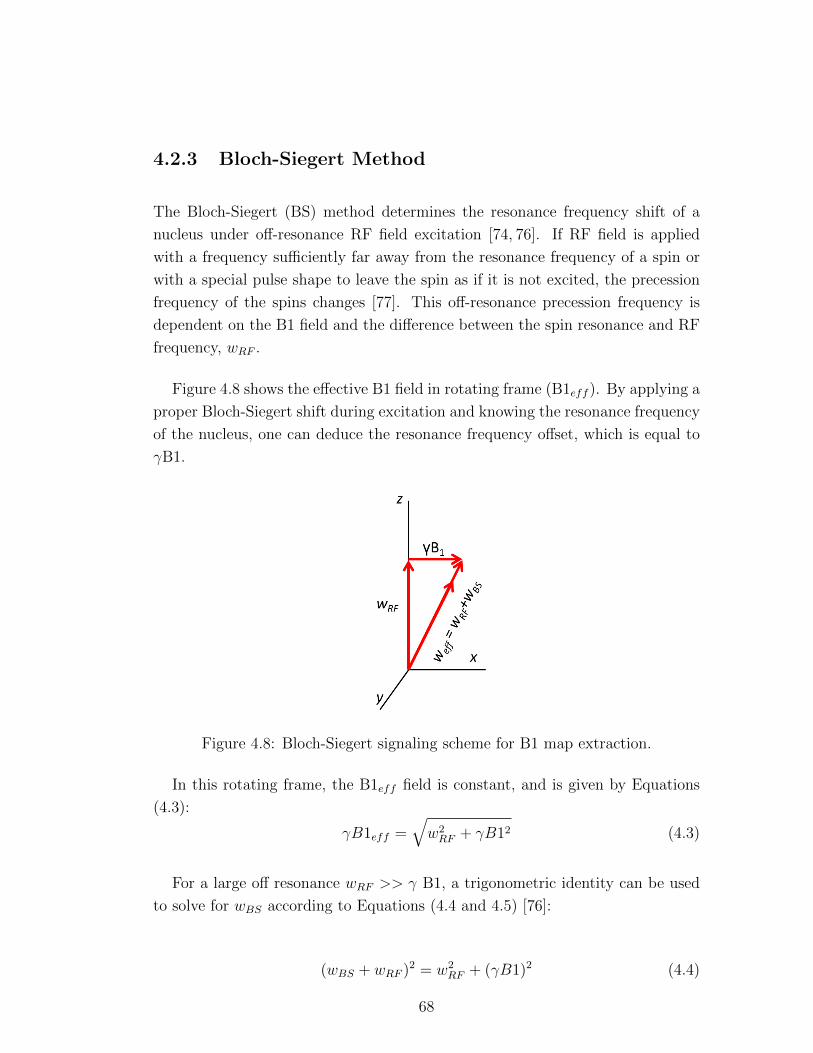
4.2.3 Bloch-Siegert Method
The Bloch-Siegert (BS) method determines the resonance frequency shift of a
nucleus under off-resonance RF field excitation [74, 76]. If RF field is applied
with a frequency sufficiently far away from the resonance frequency of a spin or
with a special pulse shape to leave the spin as if it is not excited, the precession
frequency of the spins changes [77]. This off-resonance precession frequency is
dependent on the B1 field and the difference between the spin resonance and RF
frequency, wRF .
Figure 4.8 shows the effective B1 field in rotating frame (B1eff ). By applying a
proper Bloch-Siegert shift during excitation and knowing the resonance frequency
of the nucleus, one can deduce the resonance frequency offset, which is equal to
γB1.
Figure 4.8: Bloch-Siegert signaling scheme for B1 map extraction.
In this rotating frame, the B1eff field is constant, and is given by Equations
(4.3):
γB1eff =√w2RF + γB12 (4.3)
For a large off resonance wRF >> γ B1, a trigonometric identity can be used
to solve for wBS according to Equations (4.4 and 4.5) [76]:
(wBS + wRF )2 = w2RF + (γB1)2 (4.4)
68
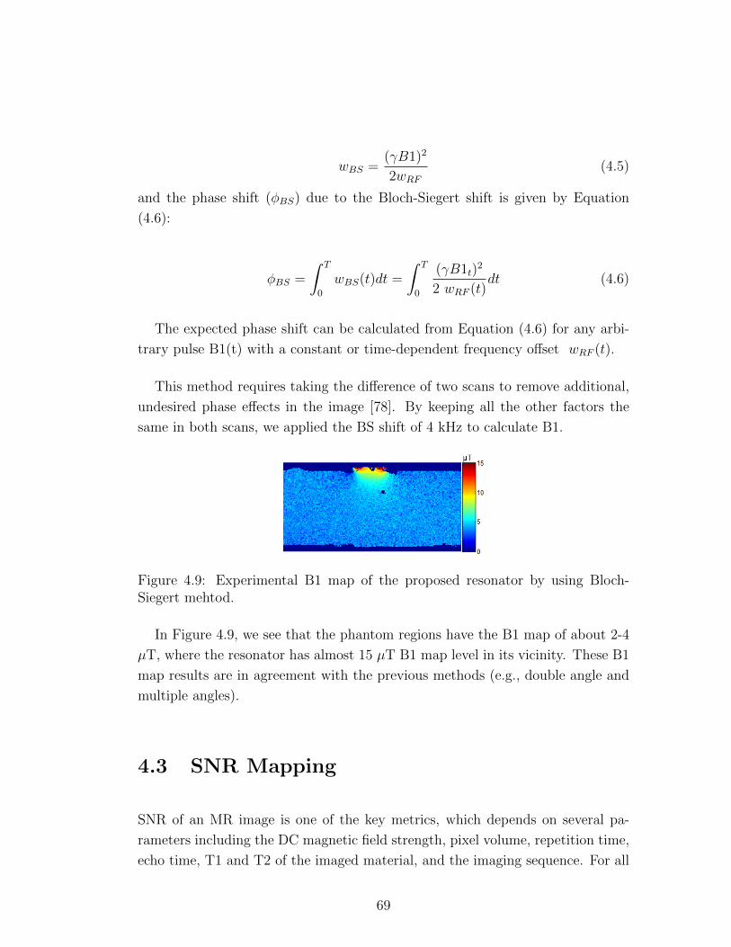
wBS =(γB1)2
2wRF(4.5)
and the phase shift (φBS) due to the Bloch-Siegert shift is given by Equation
(4.6):
φBS =
∫ T
0
wBS(t)dt =
∫ T
0
(γB1t)2
2 wRF (t)dt (4.6)
The expected phase shift can be calculated from Equation (4.6) for any arbi-
trary pulse B1(t) with a constant or time-dependent frequency offset wRF (t).
This method requires taking the difference of two scans to remove additional,
undesired phase effects in the image [78]. By keeping all the other factors the
same in both scans, we applied the BS shift of 4 kHz to calculate B1.
Figure 4.9: Experimental B1 map of the proposed resonator by using Bloch-Siegert mehtod.
In Figure 4.9, we see that the phantom regions have the B1 map of about 2-4
µT, where the resonator has almost 15 µT B1 map level in its vicinity. These B1
map results are in agreement with the previous methods (e.g., double angle and
multiple angles).
4.3 SNR Mapping
SNR of an MR image is one of the key metrics, which depends on several pa-
rameters including the DC magnetic field strength, pixel volume, repetition time,
echo time, T1 and T2 of the imaged material, and the imaging sequence. For all
69

the other parameters kept constant, having a higher B1 value will result in bet-
ter SNR performance. This can be achieved by using improved antenna systems
and/or using passive wireless coils (as proposed in this thesis work) closer to the
imaged volume. Since the B1 performance of the proposed resonator has been
discussed earlier, here we will mainly focus on the SNR improvement performance
of this structure.
SNR calculation of complex valued MR images was proposed by Henkelman
[79]. A predetermined slice is imaged several times to properly see the effect
of noise in the consecutive slices. Graphical representation of this method is
illustrated in Figure 4.10.
Figure 4.10: Representation of noise calculation for complex valued pixels.
Here, Sj is the complex signal strength of the jth pixel and SNj is the noise
signal in that pixel for the given image frame. It is assumed that the noise signal
has a Gaussian distribution with a zero mean. Hence, different images of the same
frame are averaged to find the mean of the signal level of each pixel. Similarly,
the standard deviation of these images for a given pixel represents the complex
noise. For the regions with sufficiently higher signal intensities (e.g., Sj >> SNj),
this method converges to real values quickly.
To implement this method, we prepared an MR imaging set-up with the same
phantom as defined earlier. MR images were acquired by using GRE with an
80 mm × 80 mm FOV in transverse plane, a 2 mm slice thickness, TR/TE of
100 ms/10 ms, a 260 Hz pixel bandwidth, and a flip angle of 10 and applying
different imaging resolution and numbers of acquisition (NA) to observe the effect
of voxel size on SNR. Figure 4.11 depicts the SNR distribution of this set-up with
70
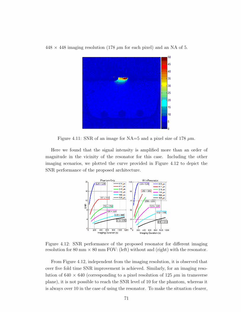
448 × 448 imaging resolution (178 µm for each pixel) and an NA of 5.
Figure 4.11: SNR of an image for NA=5 and a pixel size of 178 µm.
Here we found that the signal intensity is amplified more than an order of
magnitude in the vicinity of the resonator for this case. Including the other
imaging scenarios, we plotted the curve provided in Figure 4.12 to depict the
SNR performance of the proposed architecture.
Figure 4.12: SNR performance of the proposed resonator for different imagingresolution for 80 mm × 80 mm FOV: (left) without and (right) with the resonator.
From Figure 4.12, independent from the imaging resolution, it is observed that
over five fold time SNR improvement is achieved. Similarly, for an imaging reso-
lution of 640 × 640 (corresponding to a pixel resolution of 125 µm in transverse
plane), it is not possible to reach the SNR level of 10 for the phantom, whereas it
is always over 10 in the case of using the resonator. To make the situation clearer,
71
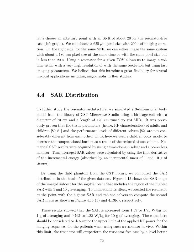
let”s choose an arbitrary point with an SNR of about 20 for the resonator-free
case (left graph). We can choose a 625 µm pixel size with 200 s of imaging dura-
tion. On the right side, for the same SNR, we can either image the same system
with about a 180 µm pixel size at the same time or with the same pixel size but
in less than 20 s. Using a resonator for a given FOV allows us to image a vol-
ume either with a very high resolution or with the same resolution but using fast
imaging parameters. We believe that this introduces great flexibility for several
medical applications including angiographs in flow studies.
4.4 SAR Distribution
To futher study the resonator architecture, we simulated a 3-dimensional body
model from the library of CST Microwave Studio using a birdcage coil with a
diameter of 70 cm and a length of 120 cm tuned to 123 MHz. It was previ-
ously proven that the tissue parameters (hence, RF characteristics) of adults and
children [80, 81] and the performance levels of different solvers [82] are not con-
siderably different from each other. Thus, here we used a children body model to
decrease the computational burden as a result of the reduced tissue volume. Nu-
merical SAR results were acquired by using a time-domain solver and a power loss
monitor. Time-averaged SAR values were calculated by using the time derivative
of the incremental energy (absorbed by an incremental mass of 1 and 10 g of
tissues).
By using the child phantom from the CST library, we computed the SAR
distribution in the head of the given data set. Figure 4.13 shows the SAR maps
of the imaged subject for the sagittal plane that includes the region of the highest
SAR with 1 and 10 g averaging. To understand its effect, we located the resonator
at the point with the highest SAR and ran the solvers to compute the second
SAR maps as shown in Figure 4.13 (b) and 4.13(d), respectively.
These results showed that the SAR is increased from 1.09 to 1.91 W/kg for
1 g of averaging and 0.763 to 1.22 W/kg for 10 g of averaging. These numbers
should be considered to determine the upper limit of the applied RF power for the
imaging sequences for the patients when using such a resonator in vivo. Within
this limit, the resonator will outperform the resonator-free case by a level better
72
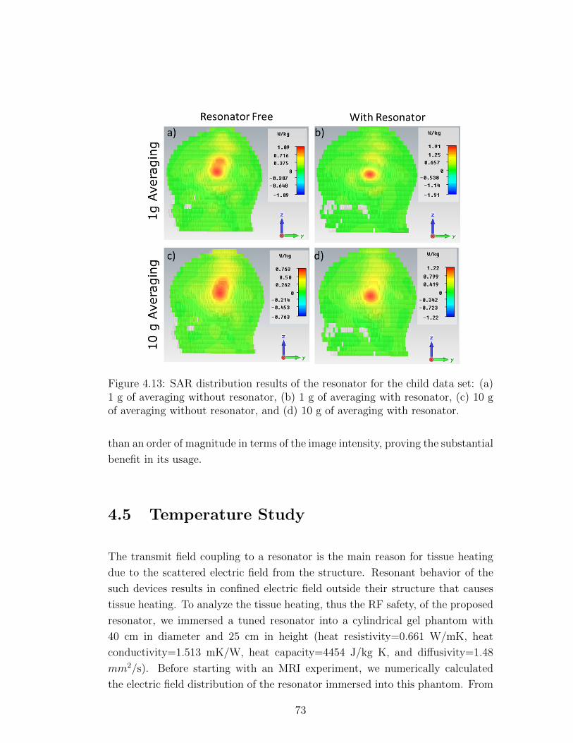
Figure 4.13: SAR distribution results of the resonator for the child data set: (a)1 g of averaging without resonator, (b) 1 g of averaging with resonator, (c) 10 gof averaging without resonator, and (d) 10 g of averaging with resonator.
than an order of magnitude in terms of the image intensity, proving the substantial
benefit in its usage.
4.5 Temperature Study
The transmit field coupling to a resonator is the main reason for tissue heating
due to the scattered electric field from the structure. Resonant behavior of the
such devices results in confined electric field outside their structure that causes
tissue heating. To analyze the tissue heating, thus the RF safety, of the proposed
resonator, we immersed a tuned resonator into a cylindrical gel phantom with
40 cm in diameter and 25 cm in height (heat resistivity=0.661 W/mK, heat
conductivity=1.513 mK/W, heat capacity=4454 J/kg K, and diffusivity=1.48
mm2/s). Before starting with an MRI experiment, we numerically calculated
the electric field distribution of the resonator immersed into this phantom. From
73

these calculations, we determined the possible region with the highest SAR values,
where the highest region has an SAR increase of about %40.
Figure 4.14: A tuned resonator loaded into a cylindrical phantom and numeri-cally evaluated for the highest SAR regions (top left). Experimental set-up wasprepared by using the same configuration with a five fiberoptical temperaturesensing lumens located properly (top right). Here the temperature increase mea-sured by four probes is not significantly different than the reference probe (thefifth one), which was located very far from the resonator (bottom). The proposedresonator is expected to be RF safe [48].
Four fiber tips (P1-P4) of an optical thermometer (Neoptix, RF-04-1, Fiber
optical temperature sensor, Canada) were positioned inside the phantom near
the resonator as depicted in Figure 4.14. The last fiber tip, P5 was used as a
reference electrode that is located 25 cm away from the resonator. The experi-
mental set-up was exposed to a high SAR sequence (GRE: TR=2.6 ms, TE=1.5
ms, FA=50, slice thickness=200 mm, FOV =220× 220 mm2, average=32). The
74

total acquisition time was 16 min at a B1-field strength of 14 µT.
RF heating measurement of the resonator was measured under continuous high
SAR MRI pulse sequence. All the fiber sensors experienced similar temperature
raises (P1 = 2.1C, P2 = 1.7C, P3 = 1.8C, P4 = 1.7C and P5 = 1.6C).
The measured temperature difference was the highest at the point P1 with a
temperature difference of 2.1C. We may claim that the electric field distribution
of the resonator is relatively homogeneous, which is due to its thin-film loading
scheme, to lead to uniform temperature increase along with its geometry. We
experimentally observed that the maximum SAR increase was obtained with 60%
under these circumstances, which is still below the limits of U.S. food and drug
administration (FDA). Although we observed temperature increase in this study,
most of the imaging applications do not require such high SAR sequences; hence,
RF safety of the proposed resonator can possibly be attained easily.
4.6 Proof-of-Concept Demonstration Under 1.5
T
To verify the operation of the proposed resonator, a device with a 14 mm× 14 mm
footprint area was fabricated onto a Kapton polyimide film (which was thinned
down using a reactive ion etching) with an initial resonance frequency of 42 MHz
and a Q-factor of about 21. This structure was tuned to the operating frequency of
a 1.5 T Siemens Scanner located at Hacettepe University, at a resonance frequency
of 63.67 MHz. A GRE sequence with a TR of 580 ms, a TE of 14 ms, a FOV of
120 mm × 120 mm, a resolution of 256 × 256, a slice thickness of 5 mm, a pixel
bandwidth of 121 Hz and a total acquisition time of 192 s were used to determine
the location of the resonator external to a cylindrical phantom. Imaging set-up
and 1.5 T MRI images are depicted in Figure 4.15.
We clearly see that the proposed structure, once tuned to the targeted fre-
quency, can be used with different MRI platforms. Since the operating frequen-
cies of about 60 MHz is easily achievable with the footprint area of about 1 cm
× 1 cm, we believe this architecture can be used for most of the clinical MRI
scanners as an in-vivo and/or ex-vivo imaging device.
75

Figure 4.15: Schematic representation of the imaging set-up (left) and the 1.5 TMRI of the resonator that is external to the phantom (right).
76
Chapter 5
Imaging Applications
This chapter is based on and partially taken from the following publications of
the thesis author: S. Gokyar, A. Alipour, E. Unal, E. Atalar, H. V. Demir,
Magnetic resonance imaging assisted by wireless passive implantable fiducial e-
markers, IEEE Access, vol. 5, issue 1, pp. 19693-19702, (2017), doi: 10.1109/AC-
CESS.2017.2752649; S.Gokyar, A.Alipour, E.Atalar, and H.V.Demir, ”Wireless
deep-sub-wavelength metamaterial enabling sub-mm resolution magnetic reso-
nance imaging”, in revision Sensors and Actuators: A. Physical (2017); and
A.Alipour, S.Gokyar, O.Algin, E.Atalar, and H.V.Demir, ”An Inductively cou-
pled ultra-thin, flexible and passive RF resonator for MRI marking and guid-
ing purposes: clinical feasibility”, Magn. Reson. in Medicine, (2017), doi:
10.1002/mrm.26996.
5.1 MRI Marking of Subdural Electrodes
For the treatment of epilepsy disease, it is a common method to use subdural
electrodes to image defected parts of the brain, where the positioning of the
electrodes has crucial importance for the surgery [83]. Correct positioning and
high performance imaging of problematic regions improve the success rate of
this treatment and help to eliminate excess recession of the brain regions. As
mentioned earlier, clinical MRI scans are not suitable to show these electrodes
77

due to lack of 1H atoms in their content. Some magnetic content could be added
to these electrodes to make them MRI visible (actually darker), but this comes
with a loss of data and increased artifacts near them, which cannot be removed
in real time by any MRI method. Position of a non-magnetic subdural electrode
cannot thus be determined by MRI. Additional imaging modalities, e.g., X-ray,
PET and CT, are therefore required to reveal their locations correctly. The
proposed resonator here can allow for marking in MRI together with enabling
enhancement in imaging resolution without any timing parameter.
As a proof of concept demonstration, we prepared an imaging environment
with an eight-channel open surface coil array, dedicated to animal experiments,
and a rabbit used for ex-vivo imaging was placed at the scanner as shown in
Figure 5.1. Here necessary steps to obey the national laws (5199, February,
2014), ruled by European Union Directive 2010/63/EU, were applied for animal
experiments (Bilkent University, HADYEK permission, 2012/9, ext. 3). The
rabbit was positioned on the patient bed of the scanner and transverse images
were acquired for marking purposes. Images were acquired by using body coil as
the transmitter, surface coil as the receiver with a GRE sequence, 100 mm × 100
mm FOV in the transverse plane, a 256 × 256 image resolution, a 2 mm slice
thickness, TR/TE of 100 ms/10 ms, a 260 Hz pixel bandwidth, a flip angle of 3
and a total imaging duration of 29 s.
Figure 5.1: An eight-channel open surface coil system used for ex-vivo animalstudies.
Although a detailed analysis about the safety of intracranial EEG electrodes
under MRI was previously conducted [84], their magnetic content prevents us to
use them for GRE sequences. Hence, we fabricated an array of mimicked non-
magnetic subdural electrodes. To mimic the operation of subdural electrodes,
we deposited Ti/Au metals onto a 12.5 µm thick flexible polyimide film, Kapton,
with a diameter of 4 mm and combined them with the resonators by sticking them
to each other. The overall electrode-resonator structure was placed external to
78
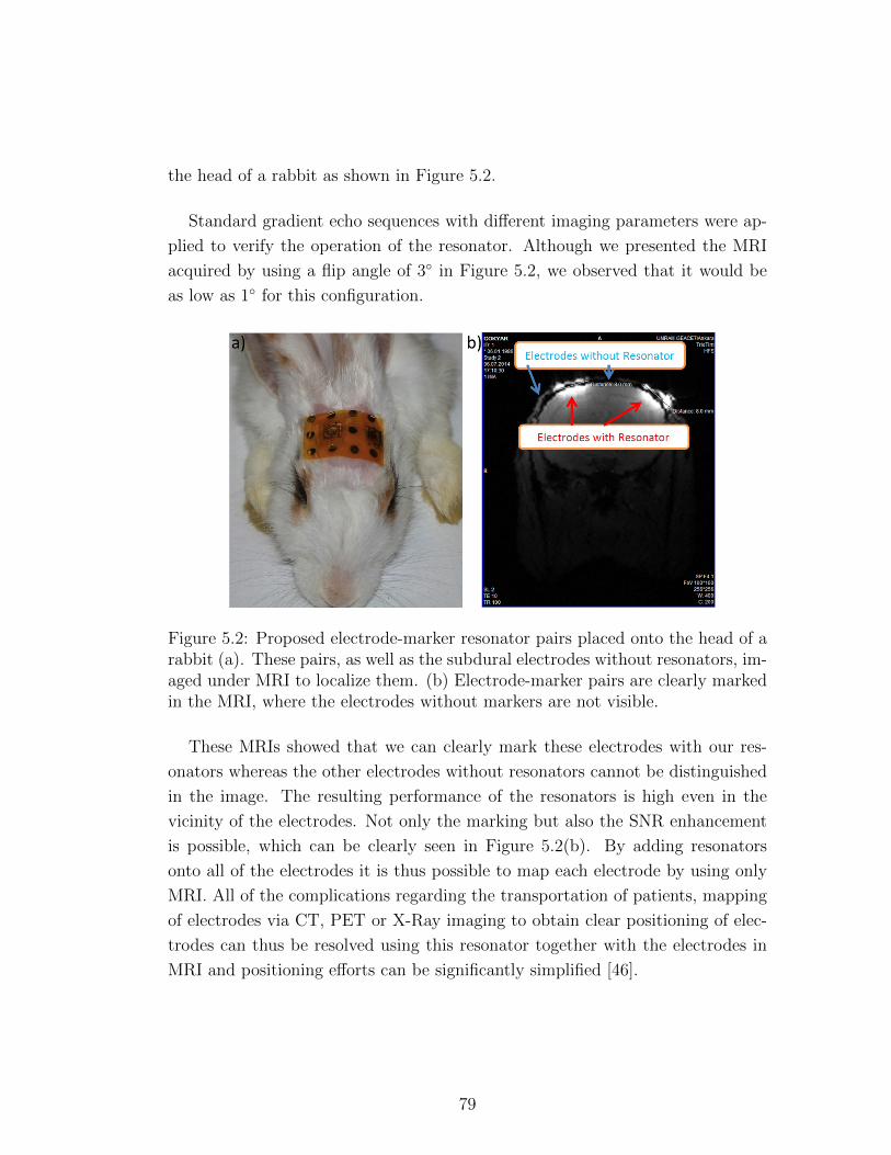
the head of a rabbit as shown in Figure 5.2.
Standard gradient echo sequences with different imaging parameters were ap-
plied to verify the operation of the resonator. Although we presented the MRI
acquired by using a flip angle of 3 in Figure 5.2, we observed that it would be
as low as 1 for this configuration.
Figure 5.2: Proposed electrode-marker resonator pairs placed onto the head of arabbit (a). These pairs, as well as the subdural electrodes without resonators, im-aged under MRI to localize them. (b) Electrode-marker pairs are clearly markedin the MRI, where the electrodes without markers are not visible.
These MRIs showed that we can clearly mark these electrodes with our res-
onators whereas the other electrodes without resonators cannot be distinguished
in the image. The resulting performance of the resonators is high even in the
vicinity of the electrodes. Not only the marking but also the SNR enhancement
is possible, which can be clearly seen in Figure 5.2(b). By adding resonators
onto all of the electrodes it is thus possible to map each electrode by using only
MRI. All of the complications regarding the transportation of patients, mapping
of electrodes via CT, PET or X-Ray imaging to obtain clear positioning of elec-
trodes can thus be resolved using this resonator together with the electrodes in
MRI and positioning efforts can be significantly simplified [46].
79

5.2 SNR Improvement for High-Resolution
MRI
Following the seminal work of Veselago [85], metamaterials were introduced for
different applications including material characterization [86], sensing [33–37,87–
89], compacting devices [90–92], and imaging of sub-wavelength features [93, 94]
from optical frequencies [95,96] to RF region [41]. Operating bandwidth of those
metamaterial devices has been typically narrow due to high Q-factor elements
used in the unit cell of their structures. Since MRI is basically a narrow band-
width imaging technique, metamaterials could be greatly attractive for MRI ap-
plications. It was indeed previously shown that metamaterial structures can
be used for RF flux guiding [97] and SNR improvement purposes [63]. These
metamaterials, in addition to conventional imaging hardware of an MRI scanner,
properly manipulates the EM fields in their vicinity to increase imaging signal
emitted from the imaged objects (e.g., tissues). However, these previous designs
are typically larger in size to be used for medical applications. As such, the design
of wireless sub-cm metamaterials to address in-vivo MRI of sub-mm features has
not been achieved to date.
High-resolution MRI (HR-MRI) suffers the fundamental problem of reduced
SNR due to decreased volume of the imaged voxels. To increase the SNR of an
MR image, several methods can be applied. These include applying a higher
DC magnetic field [98], eploying high density coil arrays with parallel imaging
techniques [99, 100], increasing the number of image acquisition and using high-
sensitivity wired coils [8, 60, 101–109]. Practically, DC field strength is prede-
termined and assumed to be constant after the installment of the main magnet.
Although using high density coil arrays with parallel imaging techniques is one
of the major breakthroughs, their performance can be increased further by using
wireless coils for in-vivo applications. Increasing the number of acquired images
increases the imaging duration and the total RF power exposure of patients, which
is not suitable for clinical imaging practices. Hence, for a predetermined DC field,
increasing SNR without increasing the total RF power exposure and imaging du-
ration becomes possible only with localized coil solutions. However, these coils
include complicated electronics (e.g., matching capacitors, solder, diodes and/or
80

cryo-cooling) and they are connected to the body of the scanner with RF ca-
bles. Thus, their application to in vivo operations is inherently challenging due
to RF heating risks [20]. Using wireless metamaterials for in-vivo MRI applica-
tions would increase the detection performance of an MRI system [40, 110, 111].
Although the previous wireless designs, including some metamaterials, achieved
this purpose to a certain extent, none of them has accomplished an electrical size
smaller than λ0/300 and a Q-factor larger than 50 simultaneously without using
cryo-cooling or lumped element thus far.
In this thesis work, to address the aforementioned problems of HR-MRI, we
showed a wireless deep sub-wavelength metastructure enabling a high Q-factor
of about 80 in free space, while using a highly compact footprint area. Here this
proposed wireless metamaterial architecture, while being electrically very small, is
demonstrated to be an excellent candidate for in-vivo MRI applications including
HR-MRI at sub-mm resolution level.
Figure 5.3: Kiwi fruit imaged to visualize its sub-mm features without (top pan-els) and with (bottom panels) using a resonator. Increasing resolution (decreasingpixel size) is necessary to resolve these sub-mm features, but this reduces SNR.Hence, smaller features cannot be clearly resolved due to noise (top row). How-ever, using a wireless resonator allows us to image these sub-mm features clearlyin its vicinity (bottom row).
To highlight the SNR improvement property (hence, imaging smaller features)
of the proposed structure, we prepared an imaging set-up by using kiwis. We
81
used a GRE sequence with a transverse imaging slice, TR/TE of 170 ms / 10 ms,
a FOV of 90 mm, a flip angle of 25, a slice thickness of 2 mm, a pixel bandwidth
of 260 Hz and resolutions of 128, 256 and 384 pixels in both x and y directions
with pixel sizes of 0.70 mm, 0.35 mm and 0.23 mm, respectively. Then, we put
the pre-mentioned resonators on top of the kiwi to highlight its sub-mm features.
From Figure 5.3, it is observed that increasing the imaging resolution (in-
creasing the imaging matrix size) results in the decreased voxel size, which in
turn reduces the SNR of the pixels. This prevents us to resolve sub-mm features.
However, using a wireless resonator in this experimental set-up allows us to image
these sub-mm features with higher resolution in its vicinity. If the limited FOV is
tolerable, then these resonators serves as a perfect candidate for high-resolution
imaging applications.
Additionally, the proposed architecture was located on a coronal plane (XZ
plane), where immersed pillars were lined in the z-direction located inside a stan-
dard head coil of the scanner as shown in Figure 5.4(a). Transverse images, with
the imaging parameters given in Section 4.1., were acquired to count each pillar
as presented in Figure 5.4. Here, we observed that the pillar array can be visible
only in the vicinity of the resonator that is in agreement with the B1+ map of the
resonator as given in Figure 5.4(c). B1+ results showed that the amplitude of the
RF magnetic field can be amplified significantly in the vicinity of the resonator.
From the MR image depicted in Figure 5.4(b), we obtained the intensity plots
along blue and red lines marked on it. From Figure 5.4(d), we observed that the
average noise level corresponds to about 50 arbitrary units (a.u.), where the signal
intensity in the neighboring region of the resonator seems to be about 1,000 a.u.
Intensity curve in blue drops down to about the noise level for the corresponding
pillars in the vicinity of the resonator. We can clearly count the number of dips
to be 13, which is the number of pillars in the array. Red curve (at 5 mm away)
shows the intensity profile far away from the resonator. It is clearly seen that the
pillars 5 mm away from the resonator are not visually separable from each other.
Here we also observed that the signal intensity is amplified by about one order
of magnitude (1,000/100) in the vicinity of the resonator. For the pillars close
to the resonator metallization, contrast to noise ratio (CNR) reaches about 15.4
(i.e., CNR=(920-150)/50), where CNR drops down to about 6.9 for the 6th and
82

Figure 5.4: MRI characterization of the tuned resonator to resolve the evenlydistributed fibers pillars, each with a diameter of 200 µm. (a) 3 T SiemensMagnetom Trio MR imaging system was used with a head coil, loaded with a bodymimicking phantom to image fibers immersed into the phantom. (b) MRI imageshows that pillars are clearly visible and can be countable in the vicinity of theresonator along the blue line (at 0.1 mm away from the resonator), whereas theyare not fully resolvable along the red line (at 5 mm away from the resonator). (c)B1+ map of the wireless metamaterial structure. (d) Red curve shows the imageintensity pattern at 5 mm away from the device and the blue curve indicates theimage intensity at 0.1 mm away from the device. The blue profile clearly resolvesall 13 of these pillars.
7th pillars. This results from the increased SNR in the proximity of the resonator,
which was also verified from its B1+ map. For the pillars away from the resonator,
CNR drops to about unity. To image smaller objects, e.g., pillars with 200 µm
diameter, SNR should be kept high enough to eliminate noise effects. The pro-
posed metamaterial architecture manipulates EM field strongly in its vicinity to
increase the SNR and this allows for MRI of sub-mm pillars with an unprece-
dented resolution for the 3 T head coils, which is otherwise not possible using
these imaging parameters [112].
83

5.3 Other Applications
The proposed resonator architecture can be used as an SNR improvement device.
This structure increases the signal level in its vicinity and improves SNR of the
image, hence making the features more visible for clinical applications. The device
would increase the signal level of any biological tissue. Operational performance
of this device is not affected by the values of imaging parameters (including the
size of image, applied signal power, imaging bandwidth, imaging duration, applied
signal duration, and echo time). From Figure 5.5, we can see that the proposed
resonator can be used as an SNR improvement device in extremities (e.g., hand
in here) as well as in head. Further systematic studies are needed to explore SNR
enhancement in such body parts.
Figure 5.5: MRI of hand without a resonator (left) and with a resonator (right).
Although the proposed architecture would eliminate the need for multimodal
imaging, it is still suitable for multimodal imaging if wanted and does not put
any direct limitation to conventional imaging practices. To prove this point, we
imaged our resonator located on top of phantom by using conventional X-ray
imaging. X-ray of the resonator, together with phantom, is presented in Figure
5.6. The resonator is: optically visible (due to construction materials of gold,
polyimide, and PDMS), MRI visible (due to the resonance behavior, exhibiting
extra-ordinary benefits as explained in the previous sections), and X-ray visible
(because of containing very thin metallic paths that absorb x-ray and do not
cause any artifacts as can be seen in Figure 5.6). Hence, we can conclude that the
proposed architecture can be used for multimodal imaging practices for clinical
applications, if desired.
84

Figure 5.6: Conventional X-ray image of a resonator loaded phantom. Both phan-tom and the resonator are visible, and unlike other metallic implants reported inthe literature, the proposed device does not cause any imaging artifacts in thisplatform. This guarantees the use of conventional methods.
85
Chapter 6
Conclusions
In this thesis, we have proposed, designed and demonstrated a thin-film loaded
helical metamaterial architecture for wireless RF applications including marking
of implants under MRI and signal level enhancement for high-resolution imag-
ing. This proposed flexible architecture is also a good candidate for replacement
of lumped capacitors and inductors in conventional systems, including interven-
tional applications, thus, leaving a room for device miniaturization and improved
flexibility. Also, the proposed architecture maintains several superior properties
such as low footprint area, high Q-factors, maintaining them even under lossy
medium loading and simultaneous negative permittivity and permeability.
It is proved that the side length of the proposed architecture can be miniatur-
ized to below 1/1500th of its free space resonance wavelength, which is the smallest
self-resonating wireless structure reported thus far to the best of our knowledge.
Additionally, it has ultra-thin vertical height, which is less than 25 µm, allowing
for flexible operation for in-vivo applications. This miniaturization is achieved
because of its cross-via metallization located among consecutive layers. Thanks
to this special geometry, the proposed structure attains high Q-factors and low
resonance frequencies simultaneously (e.g., Q-factor of about 80 for λ0/400 oper-
ation). We have shown that this proposed device has a 25 times smaller footprint
area compared to its conventional counterparts at the same operating frequency
(e.g., stacked SRR architectures). This thesis work also provides the imaging
results using a 1.5 T (64 MHz) MRI to show a proof of concept demonstration. A
86
footprint area of 14 mm × 14 mm thin-film loaded helical resonator architecture
(with a corresponding side length of 1/335th of its free space wavelength) with a
Q-factor of about 20 was demonstrated successfully.
We also observed that the conventional equivalent circuit models proposed
for SRRs are not suitable for the novel resonator architecture developed in this
thesis work. Hence, a proper equivalent circuit model was developed to calculate
the characteristic parameters of the proposed architecture. Here it was proven
that the cascaded equivalent circuit model accurately calculates the resonance
frequency and the Q-factor of the proposed resonator. This equivalent circuit
model also explains the reasoning to achieve a smaller footprint area and higher
Q-factors simultaneously. Results of this circuit model were also verified by using
numerical full-wave solver (CST Microwave Studio) and followed by experimental
RF characterization of the microfabricated devices. With this circuit model,
it was observed that the ultimate Q-factor of such a thin-film loaded helical
resonator is limited by the 1/δ of its dielectric material. We also concluded that
increasing the turn ratio (the overlap area or the turn number) of the resonator
results in the increased Q-factor because of higher effective inductance.
Unlike conventional lumped resonators, tuning of the proposed resonator archi-
tecture is easier and does not introduce complications due to its geometry (e.g.,
no soldering required, no wiring or bonding was used). This was achieved by
changing the overlapping area of the consecutive turns by partial removal of the
metallization layers. Doing so, it was demonstrated that the resonance frequency
range from 30 MHz to 5.5 GHz was achievable for a footprint area of 6 mm × 6
mm. This tuning range is extraordinarily wide compared to the tuning capability
of conventional devices reported in the literature (e.g., for SRRs < 10% tuning
is possible by changing their gap size).
Thanks to the thin-film loading scheme used in our resonator architecture,
we showed that the electric field is strongly confined inside the resonator, which
allows for reduced interaction with the environment. Hence, loading of this res-
onator with a lossy medium does not substantially degrade its performance. We
also showed that the unloaded-to-loaded Q-factor ratio for a footprint area of 8
mm × 8 mm is less than 1.7, which was previously reported to be above 2.5 for
these dimensions and frequencies in the literature.
87

The proposed device architecture was microfabricated in different implemen-
tations and sizes to verify their theoretical models. A simplified microfabrication
methodology was developed to increase the fabrication yield. Here we observed
that over 90% yield is achievable using both rigid and flexible substrates. To main-
tain biocompatibility, all of the constituent of the microfabricated devices were
selected carefully (e.g., titanium, gold, polyimide and nitrides). Additionally, the
adopted fabrication technique decreased the use of hazardous chemicals such as
photoresist, removal chemicals and hydrofluoric acid. This helps to maintain bio-
compatibility for the microfabricated devices without requiring harsh cleaning.
Although all of these steps were carefully designed, biocompatibility of the final
structure should be further verified before its final use for human studies.
In this thesis, we also showed that the proposed resonator architecture exhibits
metamaterial properties including negative εr and negative µr near its operating
frequency. Such metamaterials can be used for various applications including
miniaturization of conventional circuits, remote sensing of physical signals, sensi-
tivity improvement of receiver antennas, other medical imaging applications and
cloacking. We believe that our deep sub-wavelength resonator as a metamaterial
is also a powerful candidate for these applications.
Additionally, MRI characterization of our thin-film loaded helical resonators
showed that one order-of-magnitude B1 field enhancement is possible. This ex-
plains the signal intensity improvement and SNR improvement in the MR images
taken with these resonators. This B1 field improvement comes, however, at a cost
of SAR increase. Although the proposed resonator causes almost 50% of SAR
increase in its vicinity (for 10 g of averaging), it avoids excessive temperature in-
crease due to smaller volume of localization. Additional temperature studies were
conducted to understand their safety of the proposed structure. We found that
the maximum temperature increase was about 2.1 C for a high SAR imaging
sequence, where a reference point experiences a temperature increase of 1.6 C.
WE therefore observed that the proposed resonator architecture would be safe
for most of the clinical MRI sequences.
Finally, the microfabricated devices were also demonstrated for various MRI
applications including subdural electrode marking, SNR improvement and mul-
timodal imaging. Here we demonstrated that the marking of subdural electrodes
under MRI is possible without requiring any other imaging method when using
88

such a resonator. Such compatibility increases the reliability of treatment and
decreases the risks due to multi-platform dependent discrepancies. In addition to
this simplification, we also found that the proposed structure does not put any
limitation to conventional imaging modalities such as X-ray. An x-ray image of
the resonator was provided to show this capability.
In summary, the findings of this thesis work reflect that the proposed thin-film
loaded helical metamaterial architecture is a strong candidate for various appli-
cations including marking, SNR improvement, and improving the performance of
conventional devices by field localization. We believe that this architecture holds
a great promise for future applications such as smart implants and other imaging
technologies.
6.1 Contributions to the Literature
The author of this thesis, Saym Gkyar, made the following contributions during
the time of this thesis. These contributions to the literature are summarized
below one by one, along with the author’s individual contribution. This thesis
including some of these contributions as reported and identified below:
1. S.Gokyar, A. Alipour, E. Unal, E. Atalar, H. V. Demir, “Magnetic reso-
nance imaging assisted by wireless passive implantable fiducial e-markers”,
IEEE Access, vol. 5, issue 1, pp.19693-19702, 2017, doi: 10.1109/AC-
CESS.2017.2752649
In this work, passive wireless resonator architecture, namely resonator e-
marker was proposed, designed and demonstrated for subdural electrode
marking. Sayim Gokyar contributed to the design, microfabrication, and
tuning of the architectures to a predefined MRI frequency. He also con-
ducted the MRI experiments to show the proof of concept demonstration.
2. S.Gokyar, A.Alipour, E.Atalar, and H.V.Demir. “Wireless deep-
subwavelength metamaterial enabling sub-mm resolution magnetic reso-
nance imaging”, in revision, Sensors and actuators A: Physical (2017).
In this work, the wireless metamaterial resonator architecture was studied
and demonstrated with its ultrawide-band tuning properties. Sayim Gokyar
89
contributed to the design, modeling, microfabrication and tuning of the
resonator metamaterial. He also conducted the RF characterization of the
microfabricated devices followed by MRI experiments.
3. H.V.Demir, E. Unal, and S.Gokyar, “Enhancement of magnetic resonance
image resolution by using bio-compatible, passive resonator hardware”,
PCT/TR2014/000083, Republic of Korea-granted, 0157029561
4. A.Alipour, S.Gokyar, O.Algin, E.Atalar, and H.V.Demir, “An Inductively
coupled ultra-thin, flexible and passive RF resonator for MRI marking and
guiding purposes: clinical feasibility”, Magn. Reson. in Medicine, (2017),
DOI: 10.1002/mrm.26996
In this work, wireless thin-film resonator architecture was demonstrated for
passive catheter tracking purposes under MRI. Sayim Gokyar contributed
to the design and modeling of the resonator.
5. A.Alipour, V.Acikel, S.Gokyar, O.Algin, C.Oto, E.Atalar, and H.V.Demir.
“An inductively receive-only passive resonator probe decoupled using lin-
early polarized excitation for endocavity MRI imaging”, submitted to Magn.
Reson. in Medicine, (2017).
In this work, linearly polarized wireless helical resonator architecture was
demonstrated to increase transmit field decoupling for MRI applications.
Sayim Gokyar contributed to the design and modeling of the linearly po-
larized resonator. He finally reviewed the manuscript of this article in con-
junction with the other authors.
6. A. Alipour, E. Unal, S.Gokyar, and H. V. Demir. “Development of a
distance-independent wireless passive RF resonator sensor and a new tele-
metric measurement technique for wireless strain monitoring”, Sensors and
Actuators A: Physical 255, (2017): 87-93. doi:10.1016/j.sna.2017.01.010
In this work, a wireless strain sensing device was proposed, designed and
demonstrated with a distance-independent strain measurement methodol-
ogy. Sayim Gokyar contributed to the design and modeling of the proposed
sensor for numerical studies.
7. V. K. Sharma, S.Gokyar, Y. Kelestemur, T. Erdem, E. Unal, and
H. V. Demir. “Manganese doped fluorescent paramagnetic nanocrys-
tals for dual-modal imaging”, Small 10, no. 23, 4961-966, (2014):
90

doi:10.1002/smll.201401143
In this work, nano-crystals that are suitable for multimodal imaging (T1
and T2) and can be used as a new-generation contrast agents were pro-
posed, synthesized and demonstrated for MRI applications. Sayim Gokyar
designed and conducted the MRI experiments to measure the T1 and T2
parameters of these nano-crystals. He also contributed to the MRI charac-
terization.
8. S.Fardindoost, A.Alipour, S. Mohammadi,S.Gokyar, R.Sarvari, A.Irajizad,
and H.V.Demir, “Flexible strain sensors based on electrostatically actuated
graphene flakes”, Journal of Micromechanics and Microengineering, 25 (7),
075016, (2015).
In this work, nested-comb architectures were microfabricated onto a flexible
substrate by using graphene flakes to increase the Q-factor of resonators.
Hence, better sensitivities were achieved with these flexible sensors. Sayim
Gokyar contributed to the microfabrication and RF characterization of the
proposed graphene sensors.
9. A.Alipour, S.Gokyar, E.Unal, and H.V.Demir, “Thin-film resonator
marker for interventional MRI”, MRI-Balkan, Ankara, (2014).
In this work, thin-film resonator architecture was investigated for interven-
tional MRI applications. The first characterization results of the proposed
architecture were reported. Sayim Gokyar contributed to the design, mi-
crofabrication, and tuning of the device.
10. A.Alipour, S.Fardindoost, S. Mohammadi, S.Gokyar, R.Sarvari, A.Irajizad,
and H.V.Demir, “Ultrasensitive flexible graphene-based resonator sensor for
strain sensing”. IEEE RWW, Austin (2016).
In this work, the resonator architecture was microfabricated with extraordi-
narily high Q-factors to achieve ultrasensitive sensors. Sayim Gokyar con-
tributed to the microfabrication and RF characterization of the proposed
graphene sensors.
91
Bibliography
[1] P. C. Lauterbur, “Image Formation by Induced Local Interactions: Examples
Employing Nuclear Magnetic Resonance”, Nature, 242, 190-191, 16 March
1973
[2] F. Bloch, W. W. Hansen, and M. Packard, “Nuclear Induction”, Physical
Review Letters, 69, 127, 1946
[3] E. M. Purcell, H. C. Torrey and R. V. Pound, “Resonance Absorption by
Nuclear Magnetic Moments in a Solid”, Physical Review Letters, 69, 37, 1946
[4] “Nobel Prize for Physics”, 1952, Nature 170, 911-912, 29 November 1952
[5] https : //www.nobelprize.org/nobelprizes/medicine/laureates/2003/press.html,
Last Accessed: Oct. 2017
[6] Atalar, E., Bottomley, P. A., Ocali, O., Correia, L. C. L., Kelemen, M. D.,
Lima, J. A. C. and Zerhouni, E. Atalar, “High resolution intravascular MRI
and MRS by using a catheter receiver coil”, Magn. Reson. Med., 36: 596-605.
doi:10.1002/mrm.1910360415
[7] K. Segkhoonthod, R. R. A. Syms and I. R. Young, “Design of Magneto-
Inductive Magnetic Resonance Imaging Catheters”, IEEE Sensors Journal,
Vol. 14, No: 5, May 2014
[8] R. R. A. Syms, I. R. Young, M. M. Ahmad, M. Rea, C. A. Wadsworth,
S. D. Taylor-Robinson, “Thin-Film Detector System for Internal Magnetic
Resonance Imaging”, Sensors and Actuators A, 163, 15-24, 2010
[9] R. R. A. Syms, I. R. Young, C. A. Wadsworth, S. D. Taylor-Robinson and
M. Rea, “Magnetic Resonance Imaging Duodenoscope”, IEEE Transactions
on Biomedical Engineering, Vol. 60, No:12, Dec. 2013.
92

[10] K. Segkhoonthod, R. R. A. Syms and I. R. Young, “Design of Magneto-
Inductive Magnetic Resonance Imaging Catheters”, IEEE Sensors Journal,
Vol. 14, No: 5, May 2014.
[11] R. R .A. Syms, I. R. Young, M. M. Ahmad, S. D. Taylor-Robinson and M.
Rea, “Magneto-Inductive Catheter Receiver for Magnetic Resonance Imag-
ing”, IEEE Trans. On Biomedical Engineering, Vol. 60, No:9, Sept. 2013
[12] J. E. Baumgartner, “MRI-Compatible Fiducial Markers and Methods for
Using the Same”, US PATENT NO: US 20150011868 A1, January 2015.
[13] E. R. Cosman, T. S. Roberts, “CT and MRI Visible Index Markers for
Stereotactic Localization”, US PATENT NO: US 6,419,680 B1, July 2002.
[14] C. Guihua, C. Wenjie, W. Zhuang, Y. Renxu, L. Hua, G. Jinming, S. Xintao,
“MRI-visible polymeric vector bearing CD3 single chain antibody for gene
delivery to T cells for immunosuppression”, Biomaterials, 30 (2009): 1962-
1970
[15] P. Pang, C. Wu, M. Shen, F. Gong, K. Zhu, Z. Jiang, S. Guang, H. Shan, X.
Shuai, “An MRI-Visible Non-Viral Vector Bearing GD2 Single Chain Anti-
body for Targeted Gene Delivery to Human Bone Marrow Mesenchymal Stem
Cells”, PLoS ONE 8(10): e76612. doi:10.1371/journal.pone.0076612
[16] C. C. Parker, A. Damyanovich, T. Haycocks, M. Haider, A. Bayley, C. N.
Catton, “MRI in the Radiation Treatment Planning of Localized Prostate
Cancer Using Intra-Prostatic Fiducial Markers for CT Co-Registration”, Ra-
dioterapy and Oncology 66: 217-224, 2003.
[17] J.W. Gilbert, G.R. Wheeler, G.B. Richardson, S.L. Herder, G.E. Mick, K.
Gyarteng-Dakwa, C.M. Kenney, P.G. Broughton, “Guidance of magnetic res-
onance imaging and placement of skin-marker localization devices”, J. Neu-
rosurg. Sci.,55(2):85-8, 2011.
[18] M. Burl, G. A. Coutts and I. R. Young, “Tuned Fiducial Markers to Identify
Body Locations with Minimal Perturbation of Tissue Magnetization”, Magn.
Res. On Med., 36:491-493, 1996.
[19] H. H. Quick, M. O. Zenge, S. Massing, M. E. Ladd, “Wireless Active Catheter
Visualization: Passive Decoupling Methods and Their Impact on Catheter
Visibility”,Proc. Intl. Soc. Magnetic Resonance in Medicine, 13 (2005)
93
[20] Paul A. Bottomley, “Turning Up the Heat on MRI”, J. Am. Coll. Radiol.,
5 (7), 853-855, July 2008.
[21] G. Thormer, N. Garnov, M. Moche, J. Haase, T. KAhn and H. Busse, “Simul-
taneous 3D localization of multiple MR-visible markers in fully reconstructed
MR images: proof-of-concept for subsecond position tracking”, Magnetic Res-
onance Imaging, 30, 2012, 371-381,
[22] M. Rea, D. McRobbie, H. Elhawary, Z. T. H. Tse, M. Lamperth, I. R. Young,
“Sub-pixel Localisation of passive micro-coil fiducial markers in interventional
MRI”, Magn Reson Mater Phy, 22: 71, 2009, doi:10.1007/s10334-008-0143-1.
[23] S. S. Dalal, E. Edwards, H. E. Kirsch, N. M. Barbao, R. T. Knight,
S. S. Nagarajan, “Localization of neurosurgically implanted electrodes via
photograph-MRI radiograph coregistration”, Journal of Neuroscience Meth-
ods, 174 (2008): 106-115
[24] P. S. LaViolette, S. D. Rand, M. Raghavan, B. M. Ellingson, K. M.
Schmainda and W. Mueller, “Three-Dimensional Visualization of Subdural
Electrodes for Presurgical Planning”, Neurosurgery, 68, 152-161, March 2011.
[25] M. A. Silberbusch, M. I. Rothman, G. K. Bergey, G. H. Zoarski and M. T.
Zagardo, “Subdural Grid Implantation for Intracranial EEG Recording: CT
and MR Appearance”, AJNR 19:1089-1093, June 1998
[26] J. X. Tao, S. Hawes-Ebersole, M. Baldwin, S. Shah, R. K. Erickson, J.
S. Ebersole, “The accuracy and reliability of 3D CT/MRI co-registration in
planning epilepsy surgery”, Clinical Neurophysiology, 120 (2009): 748-753
[27] B. J. Erickson, C. R. Jack, “Correlation of Single Photon Emission CT with
MRI Data Using Fiduciary Markers”, AJNR, 14: 713-720, 1993.
[28] M. Nelles, R. Koenig, J. Kandyba, C. Schaller, H. Urbach, “Fusion of MRI
and CT with subdural grid electrodes”, Zentralbl Neurochirurgie, 65(4), 174-9,
November 2004.
[29] Dwight G. Nishimura, “The Principles of Magnetic Resonance Imaging”,
Copyright April 1996 by Dwight G. Nishimura, Stanford University, USA, pp
114, April, 1996
94
[30] National Magnetic Resonance Research center,
http://umram.bilkent.edu.tr/
[31] L. Wen-Tao, Z. Dong-Lin, and T. Xin, “A novel approach to designing
cylindrical-surface shim coils for a superconducting magnet of magnetic reso-
nance imaging”, Chin. Phys., B Vol. 19, No. 1, 018701, 2010.
[32] J. M. Jin, “Electromagnetic Analysis and Design in Magnetic Resonance
Imaging”, CRC Press, September 29, 1998, ISBN 9780849396939
[33] A.Daliri, A.Galehdar, S.John, C.H.Wang, W.S.T.Rowe, K.Ghorbani, “Wire-
less strain measurement using circular microstrip patch antennas”, Sensors
and Actuators: A Physical, 184 (2012), 86-92
[34] R. Melik, E. Unal, N. K. Perkgoz, C. Puttlitz, H. V. Demir, “Metamaterial-
based wireless strain sensors”, Applied Physics Letters, 95, 011106 (2009)
[35] R. Melik, E.Unal, N. Kosku Perkgoz, B. Santoni, D. Kamstock, C. Puttlitz,
and H. V. Demir, “Nested Metamaterials for Wireless Strain Sensing”, IEEE
Journal of Special Topics in Quantum Electronics (special issue on Metama-
terials), 16, 450 (2010)
[36] R. Melik, E.Unal, N. Kosku Perkgoz, C. Puttlitz, and H. V. Demir, “Meta-
material based telemetric strain sensing in different materials”, Optics Ex-
press, 18, 5000 (2010)
[37] R. Melik, E.Unal, N. Kosku Perkgoz, C. Puttlitz, and H. V. Demir, “Flexi-
ble Metamaterials for Wireless Strain Sensing”, Applied Physics Letters, 95,
181105 (2009)
[38] Q.Y.Tang, Y.M.Pan, Y.C.Chan, K.W.Leung, “Frequency-tunable soft com-
posite antennas for wireless strain sensing”, Sensors and Actuators: A Phys-
ical, 179 (2012), 137-145
[39] F.Bilotti, A.Toscano, L.Vegni “Design of Spiral and Multiple Split-Ring Res-
onators for the Realization of Miniaturized Metamaterial Samples”, IEEE
Transactions on Antennas and Propagation, Vol: 55, Issue: 8, Aug. 2007,
DOI: 10.1109/TAP.2007.901950
[40] J. C. Ginefri, A. Rubin, M. Tatoulian, M. Woytasik, F. Boumezbeur, B. Dje-
mai, M. Poirier-Quinot, F. Lethimonnier, L. Darrasse, E. Dufour-Gergam.,
95

“Implanted, inductively-coupled, rf coils fabricated on flexible polymeric ma-
terial: Application to in vivo rat brain MRI at 7T”, Journal of Magnetic
Resonance, 224, (2012), 61-70
[41] M. J. Freire, R. Marques, “Near-field imaging in the megahertz range by
strongly coupled magnetoinductive surfaces: Experiment and ab initio anal-
ysis”, Journal of Applied Physics, 100, 063105 (2006)
[42] E. Ekmekci, K. Topalli, T. Akin and G. Turhan-Sayan, “A tunable multi-
band metamaterial design using micro-split SRR structures”, Optics Express,
Vol. 17, No. 18 (2009)
[43] M. M. Ahmad et al, “Catheter-based flexible microcoil RF detectors for
internal magnetic resonance imaging”, Journal of Micromechanics and Mi-
croengineering, 19 (2009), 074011
[44] F. Taffoni, D. Formica, P. Saccomandi, G. D. Pino and E. Schena, “Op-
tical Fiber-Based MR-Compatible Sensors for Medical Applications: An
Overview”, Sensors, 13, 14105-14120, (2013), doi:10.3390/s13101410105
[45] S. Gokyar, “Novel Implantable Distributively Loaded Flexible Resonators
for MRI”, M.Sc. Thesis, Bilkent University, Ankara, August 2011
[46] S. Gokyar, A. Alipour, E. Unal, E. Atalar, H. V. Demir, “Magnetic
Resonance Imaging Assisted by Wireless Passive Implantable Fiducial e-
Markers”, IEEE Access, Vol. 5, Issue 1, pp.19693-19702, December 2017, doi:
10.1109/ACCESS.2017.2752649
[47] A.Alipour, S.Gokyar, O.Algin, E.Atalar, and H.V.Demir, “An Inductively
coupled ultra-thin, flexible and passive RF resonator for MRI marking and
guiding purposes: clinical feasibility”, Magn. Reson. in Medicine, 17 Novem-
ber 2017, DOI: 10.1002/mrm.26996
[48] A. Alipour, “Wireless Thin Film Microwave Resonators for Sensing and
Marking”, PhD. Dissertation, Bilkent University, Ankara, May 2017
[49] J.D.Baena, J.Bonache, F.Martin, R. Marques Sillero, F. Falcone, T.
Lopetegi, M. A. G. Laso, J. Garcia-Garcia, I. Gil, M. F. Portillo, M. Sorolla,
“Equivalent-circuit models for split-ring resonators and complementary split-
ring resonators coupled to planar transmission lines”, IEEE Transactions On
Microwave Theory and Technology, Vol. MTT-53 (2005), 1451-1461
96

[50] B. Ozbey, A. Altintas, H. V. Demir, V. B. Erturk, “An Equivalent Circuit
Model for Nested Split-Ring Resonators”, IEEE Transactions on Microwave
Theory and Techniques, 65, 3733 (2017).
[51] Khennouche M. S., Gadot F., Lustrac A., Quinot M. P., Darrasse L., Ginefri
J. C., “The use of metamaterials: a solution to improve the performance of Ra-
diofrequency Coil for Magnetic Resonance Imaging (MRI)?”, Metamorphose-
VI, 468-470, 2011
[52] Inder Bahl, “Lumped Elements for RF and Microwave Circuits”, Artech
House, ISBN-13: 978-1580533096, 2003
[53] S.S.Mohan, M.Hershenson, “Simple accurate expression for planar spiral in-
ductances”, IEEE Journal of Solid State Circuits, Vol. 34-10 (Oct. 1999),
1419-1424
[54] R. Marques, L. Jelinek, F. Mesa, “Negative Refraction From Balanced Quasi-
Planar Chiral Inclusions”, Microwave and Optical Technology Letters, Vol. 49,
No. 10 (2007)
[55] F. W. Grover, “Inductance Calculations: Working Formulas and Tables”,
Dover Phoenix Ed., 2004
[56] J. T. Vaughan, J. R. Griffiths, “RF Coils for MRI“, Wiley, 2010, UK, pp
17-25
[57] A.L.Coutrot, E. Dufour-Gergam, E. Martincic, J.P. Gilles, J.P. Grandchamp,
J.M. Quemper, A. Bosseboeuf, F. Alves, B. Ahamada, “Electromagnetic
micro-device realized by electrochemical way”, Sensors and Actuators A, 91
(2001), 80-84
[58] J. C. Ginefri, E. Durand, L. Darrasse, “Quick Measurement of Nuclear Mag-
netic Resonance Coil Sensitivity with a Single-Loop Probe”, Review of Scien-
tific Instruments, 70, 4730, 1999
[59] B. Keil, J. N. Blau, S. Biber, P. Hoecht, V. Tountcheva, K. Setsompop, C.
Triantafyllou and L. L. Wald, “A 64 Channel 3T Array Coil for Accelerated
Brain MRI”, Magnetic Resonance in Medicine, 70: 248-258, 2013
[60] E.M.Kardoulaki, R.R.A.Syms, I.R.Young, M.Rea, W.M.W.Gedroyc, “Thin-
film micro-coil detectors: Application in MR-thermometry”, Sensors and Ac-
tuators: A Physical, 226 (2015), 48-58
97

[61] X. Zhang, E. Usi, S. K. Khan, M. Sadatgol and D. O. Guney, “Extremely
Sub-wavelength Negative Index Metamaterial”, Progress in Electromagnetics
Research, Vol. 152, 95-104, 2015.
[62] C. P. Scarborough, Z. H. Jiang, D. H. Werner, C. Rivero-Baleine and C.
Drake, “Experimental demonstration of an isotropic metamaterial superlens
with a negative unity permeability at 8.5 MHz”, Applied Physics Letters, 101,
014101 (2012)
[63] M. J. Freire, R. Marques, L. Jelinek, “Experimental Demonstration of a u=-1
metamaterial lens for magnetic resonance imaging”, Applied Physics Letters,
93, 231108 (2008)
[64] D. R. Smith, S. Schultz, P. Markos, C. M. Soukoulis, “Determination of
effective permittivity and permeability of metamaterials from reflection and
transmission coefficients,” Phys. Rev. B, Vol. 65, 195104, 2002.
[65] http://niremf.ifac.cnr.it/tissprop/ Last accessed on April, 2017
[66] V. Acikel, O. Ulutan, A. C. Ozen, B. Akin, Y. Eryaman and E. Atalar, “A
Novel MRI Based Electrical Properties Measurement Technique”, Proc. Intl.
Soc. Mag. Reson. Med., 21 (2013)
[67] J.B. Warntjes, O. D. Leinhard, J. West, P. Lundberg, “Rapid magnetic
resonance quantification on the brain: Optimization for clinical usage”, Magn
Reson Med., 2008, 60: 320-329.
[68] U. Katscher, P. Bornert, C. Leussler, J. S. van den Brink, “Transmit
SENSE”, Magn Reson Med., 2003, 49: 144-150
[69] Y. Zhu, “Parallel excitation with an array of transmit coils”, Magn Reson
Med., 2004, 51: 775-784
[70] D. Xu, K. F. King, Y. Zhu, G. C. McKinnon, Z. P. Liang, “Designing mul-
tichannel, multidimensional, arbitrary flip angle RF pulses using an optimal
control approach”, Magn Reson Med., 2008, 59: 547-560
[71] G. R. Morrell, “A phase-sensitive method of flip angle mapping”, Magn
Reson Med., 2008, 60: 889-894
[72] C.H. Cuningham, J.M. Pauly and K.S. Nayak, “Saturated Double-Angle
Method for Rapid B1+ Mapping”, Magn. Reson. Med., 55, 2006, 1326-1333
98

[73] J.P. Hornak, J. Szumowski, R. G. Bryant, “Magnetic field mapping”, Magn
Reson Med., 1988, 6: 158-163
[74] F. Bloch, A. Siegert, “Magnetic resonance for nonrotating fields”, Phys Rev.,
1940, 57: 522-527
[75] S. Wang, J. Murphy-Boesch, H. Merkle, A. P. Koretsky, and J. H. Duyn
“B1 Homogenization in MRI by Multi-layer Coupled Coils”, IEEE Trans Med
Imaging. 28(4): 551-554, 2009
[76] N. F. Ramsey, “Resonance transitions induced by perturbations at two or
more different frequencies”, Phys Rev. 1955, 100(4): 1191-1194
[77] M. Steffen, L. M. K. Vandersypen, I. L. Chuang, “Simultaneous soft pulses
applied at nearby frequencies”, Journal of Magn Reson., 2000, 146(2): 369-
374
[78] L. I. Sacolick, F. Wiesinger, I. Hancu, and M. W. Vogel, “B1
mapping by Bloch-Siegert shift”, Magn. Reson. Med., 63: 1315-1322
doi:10.1002/mrm.22357
[79] R. M. Henkelman, ”Measurement of signal intensities in the presence of noise
in MR images”, Med. Phys., 12(2), March/April 1985
[80] E. Conil, A. Hadjem, F. Lacroux, M. F. Wong and J. Wiart,“Variability
Analysis of SAR from 20 MHz to 2.4 GHz for Different Adult and Child
Models Using Finite-Difference Time-Domain”, Physics in Medicine and Bi-
ology, Vol. 53, 2008
[81] J. Wang, O. Fujiwara,“Comparison and Electromagnetic Absorption Charac-
teristics in Realistic Human Head Models of Adult and Children for 900 MHz
Mobile Phones”, IEEE Transactions on Microwave Theory and Techniques,
Vol. 51, No:3, March 2003
[82] M. Kozlov and R. Turner,“A comparison of Ansoft HFSS and CST Mi-
crowave Studio Simulation Software for Multi-Channel Coil Design and SAR
Estimation at 7T MRI”, PIERS Online, Vol. 6, No:4, 2010
[83] E. Asano, C. Juhasz, A. Shah, S. Sood and H. T. Chugani,“Role of Subdural
Electrocorticography in Prediction of Long Term Seizure Outcome in Epilepsy
Surgery”, Brain, A Journal of Neurology, 2009, 132, 1038-1047
99

[84] D. W. Carmichael, J. S. Thornton, R. Rodionov, R. Thornton, A. McEvoy, P.
J. Allen and L. Lemieux,“Safety of Localizing Epilepsy Monitoring Intracra-
nial Electroencephalograph Electrodes Using MRI: Radiofrequency-Induced
Heating”, Journal Of Magnetic Resonance Imaging, 28:1233”1244 (2008)
[85] Veselago V.G.,”The electrodynamics of substances with simultaneously neg-
ative values of ε and µ,”, Sov. Usp., Vol. 10, 509”514 (1968)
[86] Withayachumnankul, K.Jaruwongrungsee, A.Tuantranont, C.Fumeaux,
D.Abbott,“Metamaterial-based microfluidic sensor for dielectric characteri-
zation”, Sensors and Actuators: A Physical, 189 (2013), 233-237
[87] A.Alipour, E.Unal, S.Gokyar, H.V.Demir,“Development of a distance-
independent wireless passive RF resonator sensor and a new telemetric mea-
surement technique for wireless strain monitoring”, Sensors and Actuators:
A Physical, 255 (2017), 87-93
[88] A.K.Horestani, J.Naqui, Z.Shaterian, D.Abbott, C.Fumeaux,
F.Martin,“Two-dimensional alignment and displacement sensor based
on movable broadside-coupled split ring resonators”, Sensors and Actuators:
A Physical, 210 (2014), 18-24
[89] M. Lapine, D. Powell, M. Gorkunov, I. Shadrivov, R. Marqu”s, Y.
Kivshar,“Structural tunability in metamaterials”, Applied Physics Letters, 95,
084105 (2009), DOI: 10.1063/1.3211920
[90] F.Bilotti, L.Nucci, L.Vegni,“An SRR based microwave absorber”, Microwave
and Optical Technology Letters, 2006, 48.11: 2171-2175
[91] R. Melik, E.Unal, N. Kosku Perkgoz, C. Puttlitz, and H. V. Demir,“Circular
High-Q Resonating Isotropic Strain Sensors with Large Shift of Resonance
Frequency under Stress”, Sensors, 9, 9444, (2009)
[92] R. Melik, N. Kosku Perkgoz, E. Unal, C. Puttlitz, and H. V. Demir,“Bio-
implantable passive on-chip RF-MEMS strain sensing resonators for or-
thopaedic applications”, Journal of Micromechanics and Microengineering,
18, 115017 (2008)
[93] J. B. Pendry,“Negative Refraction Makes a Perfect Lens”, Physical Review
Letters, 85, 3966 (2000)
100

[94] D. R. Smith, J. B. Pendry, M. C. K. Wiltshire,“Metamaterials and Negative
Refractive Index”, Science, 305, 788 (2004)
[95] N. Fang, H. Lee, C. Sun, X. Zhang,“Sub”Diffraction-Limited Optical Imag-
ing with a Silver Superlens”, Science, 308, 534 (2005)
[96] F. Lemoult, N. Kaina, M. Fink, G. Lerosey,“Wave propagation control at the
deep subwavelength scale in metamaterials”, Nature Physics, Vol. 9, 2013.
[97] M. C. K. Wiltshire, J. B. Pendry, I. R. Young, D. J. Larkman, D.J. Gilderdale
and J. V. Hajnal“Microstructured Magnetic Materials for RF Flux Guides in
Magnetic Resonance Imaging”, Science, 291, 849, 51 (2001)
[98] E. Moser, M. Meyerspeer, F. Ph. S. Fischmeister, G. Grabner, H. Bauer
and S. Trattnig,“Windows on the Human Body-in vivo High-Field Magnetic
Resonance Research and Applications in Medicine and Psychology”, Sensors,
10, 5724-5757 (2010)
[99] M. Blaimer, F. Breuer, M. Mueller, R. M. Heidemann, M. A. Griswold and
P. M. Jakob,“SMASH, SENSE, PILS, GRAPPA, How to Choose the Optimal
Method”, Magnetic Resonance Imaging, Vol. 15, Nu. 4, 223-236, (August
2004)
[100] M. A. Griswold, P. M. Jakob, R. M. Heidemann, M. Nittka, V. Jellus, J.
Wang, B. Kiefer and A. Haase,“Generalized Autocalibrating Partially Parallel
Acquisitions (GRAPPA)”, Magnetic Resonance in Medicine, vol. 47, 1202-
1210, (2010)
[101] C. Baltes, N. Radzwill, S. Bosshard, D. Marek, M. Rudin,“Micro MRI of
the mouse brain using a novel 400 MHz cryogenic quadrature RF probe”,
NMR in Biomedicine, 22: 834-842, 2009, doi:10.1002/nbm.1396
[102] T. Dohi, K. Matsumoto, I. Shimoyama,“Flexible Micro Resonator for the
Magnetic Resonance Catheter”, The 13th Int. Conf. on Solid-State Sensors,
Actuators and Microsystems, Seoul, Korea, June 5-9, 2005
[103] J. Gawlitza, M. Reiss-Zimmermann, G. Th”rmer, A. Schaudinn, N. Linder,
N. Garnov, L.C. Horn, D. H. Minh, R. Ganzer, J.U. Stolzenburg, T. Kahn, M.
Moche, H. Bussea, “Impact of the use of an endorectal coil for 3 T prostate
MRI on image quality and cancer detection rate”, Nature, Scientific Reports,
7:40640 (2017), doi:””10.1038/srep40640
101

[104] P. Gonord, S. Kan, A. Leroy-Willig, and C. Wary,“Multigap parallel-plate
bracelet resonator frequency determination and applications”, Review of Sci-
entific Instruments, 65, 3363 (1994), doi: 10.1063/1.1144573
[105] P. Gonord S. Kan, A. Leroy-Willig,“Parallel Plate Split-Conductor Surface
Coil: Analysis and Design”, Magn. Reson. in Medicine, 6, 353-358 (1988)
[106] I. Lin, H. C. Yang, J.H. Chen,“Diffusion tensor imaging using a high-
temperature superconducting resonator in a 3T magnetic resonance imaging
for a spontaneous rat brain tumor”, Applied Physics Letters, 102, 063701
(2013)
[107] T.Matsunaga, Y.Matsuoka, S.Ichimura, Q.Wei, K.Kuroda, Z.Kato,
M.Esashi, Y.Haga,“Multilayered Receive Coil Produced Using a
Non-planar Photofabrication Process for an Intraluminal Mag-
netic Resonance Imaging”, Sensors and Actuators: A Physical,
http://dx.doi.org/10.1016/j.sna.2017.04.021
[108] D. Sakellariou, G. Le Goff, J. F. Jacquinot,“High-resolution, high-
sensitivity NMR of nanolitre anisotropic samples by coil spinning”, Nature,
447, 694-697 (7 June 2007)
[109] E. Laistler, M. Poirier-Quinot, S. A. Lambert, R.M. Dubuisson, O. M. Gi-
rard, E. Moser, L. Darrasse and J.C. Ginefri,“In Vivo MR Imaging of the Hu-
man Skin at Subnanoliter Resolution Using a Superconductor Surface Coil at
1.5 Tesla”, Journal of Magnetic Resonance Imaging, Vol. 41, Issue 2, 496”504
(February 2015), doi:10.1002/jmri.24549
[110] R. Kriegl, J.C. Ginefri, M. Poirier-Quinot, L. Darrasse, S. Goluch, A.
Kuehne, E. Moser, E. Laisler,“Novel Inductive Decoupling Technique for Flex-
ible Transceiver Arrays of Monolithic Transmission Line Resonators”, Mag-
netic Resonance in Medicine, 73: 1669-1681 (2015)
[111] J. A. Lehmann-Horn, J.F. Jacquinot, J. C. Ginefri, C. Bonhomme, D. Sakel-
lariou.,“Monolithic MACS micro resonators”, Journal of Magnetic Resonance,
271, (2016), 46-51
[112] S.Gokyar, A.Alipour, E.Atalar, and H.V.Demir.“Wireless deep-
subwavelength metamaterial enabling sub-mm resolution magnetic resonance
imaging”, In submission to Sensors and actuators A: Physical
102