IMAGING IR SPECTROMETER
65
SBIR Phase II IMAGING IR SPECTROMETER Final Report May 1990 SETS, Inc. Honolulu, HI 96789 Chief, Procurement Branch M/S 180-805 Contract NAS 7-1029 NASA Resident Office-JPL 4800 Oak Grove Drive Pasadena, CA 91109 Reviewed by Project Manager: __-_--_ https://ntrs.nasa.gov/search.jsp?R=19930004236 2019-01-02T20:26:42+00:00Z
Transcript of IMAGING IR SPECTROMETER

SBIR Phase II
IMAGING IR SPECTROMETER
Final ReportMay 1990
SETS, Inc.Honolulu, HI 96789
Chief, Procurement Branch
M/S 180-805Contract NAS 7-1029
NASA Resident Office-JPL4800 Oak Grove Drive
Pasadena, CA 91109
Reviewed by Project Manager: __-_--_
https://ntrs.nasa.gov/search.jsp?R=19930004236 2019-01-02T20:26:42+00:00Z
SBIR Final Report May 1, 1990
PROJECT SUMMARY
The Phase 11 research objective was to design, fabricate and test a prototype Multichannel ImagingSpectrometer for use on groundbased astronomical telescopes. Specifications for the instrument
included simultaneous operation at all channels in the spectral region _. = 1.0 to 2.5 gm at a spectral
resolution (A_/_) of 1% and with a noise equivalent power (NEP) of 10 -16 W/Hz using state-of-the-art two dimensional infrared detector arrays. Additional specifications required that theinstrument be small, transportable, capable of remote operation and provide an innovative opticaldesign to permit operation at a field of view (FOV) of 0.5 arcseconds/pixel in a mapping mode and5 arcseconds per pixel in a spot mode.
The research effort was divided into several stages. The f'n-st stage was to review the specificationsand to develop an engineering design, with associated shop drawings, for the spectrometer optical,electronic and software systems. The second stage of development was to build and test eachsubsystem and subassembly. The major subsystems are (1) the spectrometer mechanical housing(dewar) which provides environmental and mechanical stability and support for the optical bench,(2) the electronics and electronic interfaces which provide the two-way communication with thedetector and internal dewar operations, (3) the computer and interfaces which provide the hardwarefor data storage, control and remote operation and (4) the software and software interfaces which
provide the operating environment for controlling the spectrometer and preforming analysis of thedata. The research was performed primarily at the facilities of SETS, Inc., although themachining, mechanical design and fabrication of certain specialized optical and electroniccomponents were accomplished at other facilities either under contract or under our direction.
The major research result is that a low cost multichannel infrared spectrometer, or IR imagingspectrometer operating across the spectral region _. = 1.0 to 2.5 gm and meeting the specificationsof the Phase I proposal is possible and practical. A prototype IR imaging spectrometer wassuccessfully designed, fabricated and tested in the laboratory. The instrument as fabricatedoperates over the wavelength interval of 0.9 to 2.6 }.tm with an average spectral resolution of 1%.The 128 x 128 Rockwell HgCdTe array performs well within the NEP specifications. A userfriendly and versatile software program (written in C) with pull-down menus controls the operationof the spectrometer.
Other significant research findings are as follows: (1) concave holographic gratings can be used ininfrared imaging spectrometer instruments and can be designed to operate over more than onespectral octave on the same focal plane with the addition of a "step function" order sorting filter;, (2)concave holographic gratings must have the grating etched into their glass substrate for operation atliquid nitrogen temperature; (3) the use of electronic "taxi" communication connections between the
computer and the spectrometer allows for a significant distance between the spectrometer housingand the computer controller; (4) commercially available (at present) two dimensional infrared
detectors can be effective in this type of imaging spectrometer, and (5) the optical design developedunder this research considerably reduced the size of the instrument and has significant commercialapplications.
The commercial applications span private sector and government agencies. The unique opticaldesign has captured the attention of several agencies for possible use in space-basedinstrumentation particularly for planetary missions where small, lightweight, low power and
optically efficient spectrometers are required. The private sector is interested in small lightweightspectrometers for commercial applications in remote sensing from both space and aircraftplatforms. Commercial interest in the optical design has prompted SETS, Inc., to design theVIRIS TM line of imaging spectrometers which operate from 0.4 to 5.0 I.tm.
SETS, Inc. Page 1

SBIRFinal Report May 1, 1990
I. INTRODUCTION
Thisdocumentis thef'malreportby theTechnicalServicesDivision of SETS,Inc., for PhaseII inthedevelopmentof a prototypeimagingspectrometerfor useon a groundbasedtelescope.Thisresearchwascarriedoutundertheauspicesof theSmallBusinessInnovativeResearchprogramoftheNationalAeronauticsandSpaceAdministrationundercontractNAS7-1029.
The prototypeimaging spectrometerdescribedhere wasdesignedanddevelopedin two steps:PhaseI (ContractNAS7 8726)which dealtwith researchcarriedout in responseto NASA SBIRSubtopic08.27,MultichannelInfraredSpectrometerandPhaseII (1986 solicitation)which dealtwith theactualconstructionof aprototypeimagingspectrometersystemperformedin responseto aPhaseII award.
A. Phase I Research and Results
The Phase I research confirmed that a spectrometer capable of sampling simultaneously the
spectral range 1.0 to 2.5 t.tm at 1% spectral resolution with a NEP of 10 16 W/Hz was
feasible. It was found that the opportunity to develop the spectrometer would provideopportunities for research and development in the areas of infrared detector arrays, innovativeoptical designs and microelectronics. Phase I work included:
• a review of existing spectrometer designs.
• an identification and qualification of suitable two dimensional array detectors.• a review and modification of optical designs to permit maximum throughput.• a model of thermal emission from the spectrometer.
• a exploratory review of cooling options for the focal plane and optical bench.• a conceptual design of the analog and digital control electronics.• research into remote operation.• a conceptual design of the mechanical structure of the instrument.• a refined market research.
Phase I results indicated:
• that the instrument was feasible.
• that an operating prototype could be constructed under the schedule and cost constraintsof Phase II.
• that a small and growing market exists for imaging spectromters both in the commericaland government environments.
The details of the Phase I research are reported in the Phase I Final Report, dated August1987.
B. Phase II Technical Objectives
The overall objective of Phase II was to design, fabricate and test a prototype of a multi-channel infrared imaging spectrometer. To reach this goal, the project was divided into fourstages of development, each with its own objectives and schedule.
The objective of the first stage was to review the specifications and to develop an engineeringdesign with shop drawings for the spectrometer. Guidelines and specifications for each of
SETS, Inc. Page 2

SBIRFinal Report May 1, 1990
themajor componentsof the spectrometerwerethendeveloped.Fromtheseguidelinestheoptical configuration was reviewed and usedto define the mechanicaldrawings for thespectrometer.
Thesecondphaseof thedevelopmentwasto buildandtesteachof theindividual subsystemsand subassemblieswhich make up the spectrometer. These subsystemsare (1) thespectrometerhousing(dewar),(2) theelectronicsandelectronicinterfaces,(3) thecomputerand computer interfaces, and (4) the software and operations. Additionally, majorsubassembliesinclude the optical bench (grating), the detector array, the mechanicalfeedthroughs,the guiding cameraand the apertureassembly. The major subsystemandsubassembliesthat were targetedfor specialattention were the detector, the grating, thespectrometerhousing,andthecomputersystem.
C. Potential Commercial Applications
The development of this prototype imaging spectrometer has generated considerable interestamong both private sector and government agencies. The optical design (described below)using holographic optics has captured the attention of the Jet Propulsion Laboratory forpossible use in planetary mission instruments; several federal agencies interested in small,lightweight, low power imaging spectrometer systems, and the private sector which isinterested in small, lightweight, low power imaging spectrometers for use in terrestrialremote sensing from either aircraft or spaceborne platforms.
The commercial interest in imaging spectrometers based upon our optical design hasprompted SETS, Inc., to produce the VIRIS TM line of imaging spectrometer systems whichoperate from 0.4 to 5.0 gm.
II DETAILED PROJECT REVIEW
This section describes in detail the design, construction, testing and operation of the prototypeimaging spectrometer developed under the Phase II effort.
A. General Theory of Operation and Application
An imaging spectrometer produces a series of images of a scene (astronomical, terrestrial,medical, etc.) at a number of wavelengths. Each scene characterizes the photometric contrastin the scene at a particular wavelength so that spectral contrast at a variety of wavelengths canbe coregistered and studied. These scenes can be developed either by scanning throughwavelengths as the two spatial dimensions of the scene are held constant or by scanningthrough one spatial dimension of the scene and holding the other spatial dimension and thesampled wavelengths constant.
The instrument developed here produces 128 scenes at 128 different wavelengths betweenthe wavelengths of approximately 1.0 and 2.5 gm by producing a spectrally dispersed imageof a slit on a two dimensional array. Scanning the slit in the orthogonal spatial dimensionproduces a, two dimensional spatial scene at 128 wavelengths. This data set is commonlycalled an image cube which has two spatial dimensions (a picture) and one spectraldimension (the photometric contrast as a function of wavelength).
The prototype spectrometer is designed for use at an astronomical telescope, although it is notlimited to such. The light from an astronomical scene (the moon for example) is imaged ontothe slit of the spectrometer. The slit is reimaged by way of a holographic grating onto the
SETS, Inc. Page 3

SBIR FinalReport May 1, 1990
two dimensionaldetector.Thegratingproducesspectrallydispersedimagesof the slit, or inessence,128imagesof the slit, eachat a differentwavelength.A readingof thedetector(aframe)yieldsadigital measureof the intensityasa functionof wavelengthalong128pointson theslit. Thetelescopeis thensteppedin adirectionorthogonalto the lengthof theslit to apositionjust adjacentto thefirst frame. Additionalreadingsaretakenuntil a two dimensionalspatialimageis developed.
The actionof dispersingandrecordingthespectral/spatialimageis performedby theopticaldesignof thespectrometer.Thespectrometeris composedof four major subsystems:(1) thespectrometerhousing(dewar),(2) theelectronicsandelectronicinterfaces,(3) thecomputerand computer interfaces,and (4) the software and operations. Thesesubsystemwererequiredto meetthefollowing specificationsandoperatingenvironments:
Spectrometer housing: The spectrometer housing was required to withstand the mechanicalloads of normal astronomical equipment. Three important criteria must be met: (a) maintainvacuum over the course of many days, (b) permit operation of an optical bench in a cryogenicenvironment, (c) be designed to maintain a minimum of thermal loads and optical light leaks,and (d) maintain mechanical durability in the course of normal operation.
Criteria (a) and (b) are required for the operation of the two dimensional detector describedbelow. Criteria (c) is necessary to reduce the cryogenic requirements and the need forbaffling internal to the dewar. Criteria (d) is normal to most astronomical equipment. It is tobe shipped, handled, and placed on the baseplate of a telescope which will move the device toa variety of angles and positions during the course of observations. This mechanical housingmust provide a stable housing for the internal optical components which must remainoptically aligned.
Electronics and Electronic Interfaces:. The electronics and electronic interfaces are importantaspects of the spectrometer since they provide the communication for operating and acquiringdata from the spectrometer housing. Two dimensional array detectors produce a prodigiousamount of data that must be handled rapidly and accurately. The spectrometer housing isdesigned to operate at the baseplate of a telescope generally separated from the computer andother control electronics by several tens of meters. The transfer of data between the dataacquisition and data storage subsystems requires rapid electronic communications protocol.The spectrometer housing and the electronics have similar mechanical environments.
Computer and Computer Interfaces: The computer provides control and data storage for thespectrometer. The computer must be capable of rapid operation, and data acquisition andstorage. Additionally, the option of remote operation must be maintained.
Software and operation: The computer software must be useable by those not familiar withprogramming and computer operations. Also, the computer software must provide enoughprocessing capability to allow the operator to preview the data obtained by the spectrometer.Although the mechanical constraints of the computer are not as severe as those of thespectrometer housing and the electronics, the user is quite intolerant of balky programs.
B. Mechanical Subsystem
1. Mechanical Design
The mechanical design of the spectrometer has been guided by experience gained fromexisting groundbased astronomical instruments with cryogenically cooled (liquid
SETS, Inc. Page 4

SBIR FinalReport Mav 1, 1990
nitrogen,LN2) optical benchesand focal planes. Theseinstrumentsrequire that thespectrometeroptical benchbe housedin a mechanically strongvacuum dewar withnumerousoptical, electrical and mechanicalfeedthruscapableof holding, in spiteofrepeatedhandlingandmotion,a highvacuumfor periodsof at leastdaysandpreferablymonths.Themechanicalhousingmustbeconstructedsothatthermalloadson theopticalbench,andin particularthefocalplane,areminimizedto optimizethesingle-fillhold timeof the cryogenic reservoir. All optical windows must be designedto minimize theamountof scatteredlight (bothvisibleandthermal)thatenterstheinstrumentandreachestheopticalbench.
The mechanicalsystemlayout of the spectrometeris shownin the mechanicaldrawingGENASSY-100. The major mechanical subsystemsof the spectrometer are (a)spectrometerhousing(dewar),(b) thetwo cryogenicreservoirs,(c) theopticalbench,(d)the optical bench heat shield, (e) the selectableaperturesubassembly,(f) the twomechanicalfeedthrus,and(h) theevacuationvalve.
Thespectrometerhousingis madefrom a solidblock of aluminumhollowedout to formfour sidesof thebox, with two endplates,which form the other two sidesof thebox.This configurationis a compromise,minimizing numberof major vacuumtight seals(two), while still allowing greatflexibility for accessto the spectrometeroptical benchandcryogenicreservoirs.
Two copper liquid nitrogen reservoirsand associatedfill and vent tubespermit up-looking and side-lookingoperationat the telescopes.Eachreservoir,after initial cool-down, provides a hold time of about 11 hours. (SeeSection II.F.2 for a detaileddiscussionof hold timetests.)Thesolidcopperopticalbenchis situatedin direct contactwith thetwo liquid nitrogenreservoirs.Thelocationsof theopticalcomponentsandtheirassociatedfine adjustmentsarekeyedto therequirementsof theholographicgratingandthecompactsystemdesign. Factorssuchasthethermalcoefficientsof theoptical benchand themountsfor eachelementhavebeenconsidered,andrepeatedcycling of ambientto liquid nitrogentemperatureshowthe stability of theoptical pathasa result of thesedesignconsiderations.All theopticalelements(exceptnecessarilyfor thewindows andpart of theCCD guidecameratransferoptics)arecooledto the sametemperatureasthedetector.Thisdramaticallyreducesthethermalbackgroundduetotheopticalelements.
To further cut down on thermalbackgroundfrom the dewarwalls, theoptical benchisenclosedby a coppercold heatshield. Thecoppercold shieldsits on top of theopticalbench,andthereforeis cooledby theliquid nitrogenreservoirs. A coppercoversits ontop of thecold shieldwalls andcompletesthecold shieldingof the opticalbench. Theonly two portsin thecold shieldarethespectrometerentranceport andtheguidecameraexitport. To blockoff radiationfrom thecameraexitport, abaffling screenis installedinplace. (SeemechanicaldrawingDET62-100.)
Two handcrankslocatedoutsidethe spectrometerenter the spectrometerhousingbyferrofluidic feedthrus.Oneis for rotation of theaperturewheelandone is reservedforfuture usewith a focal reducer. The aperturewheelhandcrankmechanismallows theoperatorto pick the desiredaperture. Thereareeight rotary positionson the aperturewheelconsistingof four aperturesandfour blockedhalf-positions. Thefocal reducerisnot installed,but a fen-o-motormount is reservedfor this purpose. Motors may beinstalledfor both the currentaperturewheelandfocal reducerassembliesfor motorizedpositioning.
SETS,Inc. Page5

SBIRFinal Report May 1, 1990
2. VacuumHandlingProcedure
This sectiondescribestherecommendedprocedurefor achievingapropervacuumin thespectrometer.
Oncethe spectrometerhasbeenopento the atmospherefor severalhours,after closureandHe-leakcheckedfor possibleleaks,it is recommendedthatthe spectrometerhousingbepumpedfor at least48hourson ahighvacuum(<= 10-6torr) pump stationto ensureremovalof asmuchadsorbedwater vapor aspossible. For openperiodsof anhour ortwo, 12-hourpump-downis usuallyadequate.(Heatingthespectrometerto anelevatedtemperatureto acceleratepurgingof surfaceadsorbedmoleculesis not recommended,asdamageto the detectorwill result and damageto the internalelectronicsand opticalcomponentsis quitelikely. Rockwellhasnot providedsafeuppertemperaturelimits forthe detector.) The amountof outgassingis less the longer the systemis on a highvacuumstation. To help enhancethe holding time with a given chargeof cryogen,a"getter",consistingof a measureof activatedcarbon,hasbeenattachedto the insidesurfaceof the removable lid of the radiation shield. This unit will continue to effectivelycryopump residual vapors from the interior for several hours and thus will ensuremaintenance of a high vacuum (assuming no leaks to atmosphere) while the unit is atliquid nitrogen temperature. When vacuum is maintained but the instrument is allowedto warm up, it is generally good practice to re-pump the spectrometer after warm-up andbefore the next cool-down to re-establish a good base pressure and thus retain theefficiency of the getter. During cool-down the walls may feel quite cool until the getterpumping speed is established; however, if frosting is observed, abort and check forleaks.
Filling the LN2 reservoirs with the cryogen initially is a slow process because of therapid back-flow of gas from the boiling of the liquid as it is being introduced. Onceliquid begins to collect, however, the filling proceeds rapidly. The process usuallyconsumes about 4 litres of liquid. The volume of each of the reservoirs is about 750 ml.
The cryogen hold time is a very sensitive function of the quality of the ultimate vacuumachieved. Prior to closing-up, all surfaces which have been opened should be examinedfor scratches (the aluminum outer box is especially susceptible to dings and scrapes), tinyhairs and particles of dust. Any associated O-ring involved should be regreased to ensurefreedom from tiny hairs and dust particles. While the lids are removed, it isrecommended that they be stored wrapped in aluminum foil and that the exposed edges ofthe box also be so protected. When back-f'flling the instrument, it is recommended thatdry nitrogen be used.
Clean lint-free clothes and clean gloves should be used when handling vacuum surfaces.
C. Optical Design
The instrument designed in this phase emphasizes the use of optical components representingthe latest commercially available technology such as concave holographic gratings (wellcorrected for aberration), order-sorting step filters and a two dimensional array detector foruse at IR wavelengths. A concave holographic grating was used to provide a fiat focal planeand minimize aberrations. The optical components are enclosed in a vacuum coldbox andheld at an operating temperature of 77 ° K, therefore reducing the thermal background noise.The advantages of this design are simplicity, mechanical ruggedness and low mass, all ofwhich are important when designing a transportable instrument. The design is characterized
SETS, Inc. Page 6

SBIRFinal Report May 1, 1990
by a low numberof opticalelements,compactness,easeof alignment,state-of-the-artarraydetectorsandopticalefficiency.
1. OpticalElements
Figure I showsthe final optical layout of the system. The optical componentsof thesystemare: sapphireentrancewindow,pelliclebeamsplitter,apertures(two slits andtwopinholes),transferoptics for CCD camera,glasswindow for CCD cameraexit port,neutraldensityfihers for the CCD camera,folding mirror, holographicconcavegratingandorder sortingfilter. The spectraltransmissionefficiency/reflectivityof the optical
elementshavebeenmeasured.
i
i
f
I I I
1 / _j n r'_&nC" _lnr]OW
t l ! _, I '/. I I'
t It
$1it
t
i
J
Figure I. Optical System Layout
SETS, Inc.Page 7

SBIR Final Report May 1, 1990
The measuredtransmittance/reflectanceareasexpected.Theyareplottedandhavebeenincludedwith thePrototypeInstrumentPackage. Thespecificationsfor eachcomponentaredescribedbelow.
Sapphire Entrance Window." The synthetic sapphire window is the entrance port of thespectrometer. The window allows light to enter the spectrometer which is maintainedunder vacuum.
Manufacturer:.Part Number:Material:Transmission:Diameter:.Thickness:
Cosmetic Surface Quality:
Flatness:
Parallelism:
Birefringence (n o - nc):
Stress Birefringence Coefficient:
Melles Griot02 WSA 012
Anisotropic crystalline synthetic sapphire- 85% from 1-2.5 _tm (see Optics Guide 4 p. 13-2)40 mm + 0.25 mm2 mm+ 0.1 mm80-50
1_. per 25 mm at 632.8 nm over 90% of aperture3 arc min.
0.008 for visible light in direction orthogonal to the
optical axisO. 1 fringe per mm thickness at 632.8 nm and
2.43 kilograms per cm 2
Pellicle Beamspliner: A pellicle beamsplitter is mounted in front of one of the two slit
apertures. The pellicle transmits 90% and reflects 10% of the incident light withoutproducing interference fringes. The reflected light is imaged onto the CCD guide cameraso that the position in the slit of the object under study can be monitored continuously.
Manufacturer:.Part Number:Material:
Index of Refraction (nd):
Coating:
Optical Diameter:.Clear Aperture:Thickness:
Thickness Unifomaity:
Cosmetic Surface Quality:Temperature Range:Humidity Range:Frame:Frame Thickness:
Special Notes:
Melles Griot
03BPL001/01
Select optical grade nitrocellulose1.5
/01 (see Optics Guide 4 p. 13-11)- 85 - 90% transmission from 1-2.5 _m,- 40 - 80% transmission in visible region34.9 mm25.4 mm
5 _tm
2_. per 25 mm40-20-40°C to + 125°C
< 95% relative humidityHard aluminum alloy, black anodized4.8 mm
Very sensitive to acoustical disturbances, should beisolated from severe acoustical noise. Pelliclesurfaces must not be touched. Clean ONLY with a
gentle flow of clean, dry air.
Apertures: The entrance aperture is positioned on a flat reflective surface angled 45°to theincident beam. Four aperture positions are available on the rotating slit mechanism. The
SETS, Inc. Page 8

SBIR Final Report May 1, 1990
four aperturesare: (a)dull surfacedslit with pellicle beamsplitter,(b)bright surfacedslit,(c) dull pinhole, and (d) bright pinhole. The silts are for the mappingmode,and thepinholesare for the point mode. Light passingthroughthe aperturein useenterstheoptical path of the spectrometerfor dispersionand detection. Light incident on theaperturesurroundingtheslit/pinholeis reflectedtoaCCDguidecamera.
Manufacturer:Material:
Diameter:.
Clear Aperture:Slit Size:Pinhole Diameter:.
Surface Quality:
Buckbee-Mears
Bi-Metal, 0.005" copper substrate with bright nickelplating of 0.0005". Nickel surface determines theapertures of slits and pinholes.1.062" + 0.001"0.9680"+ 0.0005"
11 mm+ 0.1 mm x 133 _tm+ 2 _m(a) 140 I_m bright surface(b) 140 _m dull surface
Not specified. Hand polished with metal polish(Brasso) to form reflective surface on nickel side.
Together with the foreoptics, the size of the spectrometer aperture determines the field ofview of the system. A 40 inch (1.016 mm) telescope operated at f/35 has a plate scale of5.8 arcsecond/mm. The effective size of the slit aperture oriented at 45 ° is (taking intoaccount the thickness of the silt) 11 mm x 107 I.tm, which gives a field of view of 64arcsec x 0.62 arcsec. The effective pinhole aperture diameter is 112 _tm along the 45 °tilted spectral direction, and 140 l.tm along the spatial direction, which gives a field ofview of 0.65 arcsec x 0.81 arcsec.
The size of the apertures has been verified to conform to the manufacturer'sspecifications. The aperture sizes were measured by observing the Fraunhofer diffractionpatterns of the slit and the pinhole apertures.
Transfer Optics for CCD Guide Camera: The transfer optics for the CCD guide cameraconsist of two lenses, one inside the spectrometer and one outside the spectrometer. Thetwo lens system images the spectrometer aperture onto the CCD camera. This image isdisplayed on the camera monitor. The specifications for the two lenses are listed below,and Figure lI shows the notation system used. Table I contains the distances between the
components, and Figure IlI is the diagram of the transfer optics system.
Front Principal Plane Rear Principal Plane
ffi--_ _focal length
"_ R1
', \L',/:i I I I
I t i
Figure II. Notation for Lens.
SETS, Inc. Page 9

SBIRFinal Report May 1, 1990
Lens1: l_x)catedinsidethespectrometerdewarBiconvexcrownglasslensf = 75 mm+ 0.5%d = 50 mm + 0.5 mmtc = 10.9 mm + 0.5 mmte = 2.5 mmR1 = R2 = 76.8 mm
vp = 3.4 mmpp' =4.1 mmConcentricity < 0.15 mmCosmetic Surface Quality: 80-50Ealing Electro-optics #30-8130
Lens 2: Located outside the spectrometer dewarPlano-aspheric condenser optical crown lensf = 34.5 mm + 7%d = 38 mm+ 0.4 mmtc= 12mm+7%R1 = 18 mmR2=oo
vp=0pp' = 4.1 mm
Cosmetic Surface Quality: 80-50Maximum Service Temperature: 177°CMelles Griot #01 LAG012
Table I. Distances Between Components of CCD Camera Transfer Optics
Element Distance to next element Marginal ray height
Spectrometer 86.4 mm 0Aperture
Lens 1, vl 166.8 mm 12.8 mm
(front vertex)
Lens 2, v2 35.0 mm 8.3 mm
(front vertex)
CCD 0 0
SETS, Inc. Page 10

SBIR Final Report May 1, 1990
Spectrometer
Slit
,,_.._.- 86 4mm _--
Lens 1 Inside
Spectrometer
Outside
SpectrometerLens 2
CCD
I
166.8mm _ 35mm,.
Figure III. Layout of the CCD Camera Transfer Optics.
Exit Window for CCD Camera Transfer Optics: The glass window is the exit port forlight imaged from the spectrometer aperture onto the CCD guide camera. The window isneeded because the camera is located outside the evacuated spectrometer..
Manufacturer:.Part number:Material:Diameter:.Thickness:
Edmund Scientific CompanyN30,582Sloat optical glass34 mm3mm
Neutral Density Filters: A set of neutral density filters along with a filter wheel isprovided for the CCD guide camera. The filter wheel assembly is located outside thespectrometer, between the camera and the spectrometer.
Manufacturer:.Part Numbers:
Material:
Neutral Densities:
Diameter:.Thickness:Notes:
Oriel Corporation50271, 50272, 50273, 50274, 50275, 50281,50283, 50285
A thin metallic coating on a single glass substrate forND 0.1 - 2.0, and two metallic coatings sandwichedbetween two layers of glass with edges cemented forND 3.0 - 4.0.
ND = 0.1, 0.2, 0.3, 0.4, 0.5, 1.0, 2.0, & 4.0.The average density from 400 - 700 nm is within10% of the nominal density. Density reading from400 - 700 nm is within 5% of the average density(10% for 0.1 and 0.2 D filters).1 inch
1/16"- 1/8"
The coatings on the filter.are supposedly corrosion,scratch, and abrasion resistant. The density data foreach f'flter is supplied at 50 nm increments from400 - 1000 nm along with an average visible density.The data is contained in the neutral density filter box.
SETS, Inc. Page 11

SBIF.Final Report May,1, 1990
Thefollowing filtersarecurrentlyinstalledin thefilter wheel:
Filter Position FilterND1 none2 none3 14 25 4
Folding Mirror: The folding mirror directs light from the spectrometer aperture onto thegrating. The purpose of the mirror is to fold the optical axis to allow for compact designof the spectrometer and small angle between the incoming beam and the dispersed beamon the grating (which reduces off-axis aberrations in the optical system).
Manufacturer:Part Number:Material:
Coating:
Optical Diameter:Clear Aperture:Thickness:
Cosmetic Surface Quality:
Flatness:
Parallelism:
Special Notes:
Janos Technology, Inc.A1510-272
Silicon, single crystal
Protected Silver (see Janos catalog, 1989, p. 164)- 98% reflectance from 1-2.5 I.tm38.1 mm30.5 mm4mm40-20
_./40 at 10.6 I.tm3 min.
Use the following steps in cleaning:1. Blow off loose particles with compressed air.2. Flush surface with spectral grade methanol or
acetone.
3. If 1 and 2 don't work, soak a lens tissue with
acetone and drag tissue across outside (unused)edge of mirror. Not recommended for central(used) region of mirror. Contact manufacturerfor tough stains.
Grating: The incident light is dispersed by a concave holographic grating that is wellcorrected for aberrations over the wavelengths of interest. The object distance from theaperture to the grating is 150 mm, and the image distance from the grating to the HgCdTedetector array is 90 mm. This design allows a 100 gm slit to be imaged onto the 60 I.tmpixel. The grating is designed for operation in the mapping mode at f/15 through f/35 andfor operation in the spot mode at f/3.5. Off-axis images in the spot mode are degraded bythe fast optical system.
Manufacturer:
Grating Number:Part Number:Material:
Groove Frequency, N:Order used, M:Radius of Curvature:
Focal Length:
American Holographic, Inc.490.327399D
Pyrex, fine annealed substrate
Bakelite photoresist, gold top coating51 grooves/mm-1ll2mm56mm
SETS, Inc. Page 12

SBIRFinal Report May 1, 1990
EntranceSlitDistance:Angleof Incidence:RLD bestfit:Diameter:ClearAperture:Thickness:CosmeticSurfaceQuality:
150mm3.6°0.219663e-0.015807knm/l.tm50mm44mm12.3mm60-40concavesurface,commercialpolishbackside
TableII providestheray-tracedcharacteristicsof theIR gratingoperatedat f/35 for threepoints alonga 10mm long slit: center(0 mm), midpoint (2.5 mm), andend (5.0 mm).Table III providesthe characteristicsof the IR gratingat t"/3.5for the centerof the slitonly. Theseconditionscovertherangeof operationof thespectrometerfor bothmappingand point mode. Useat other f numbers,suchas f/10, would fall betweenthesetwoexamples.
In these tables,pixel indicates the height of the pixel (in the spatial dimension orperpendicularto the slit) andprovidesan ideaof the imagequality. The quality in thespectral dimension is given in the column labeled Band Pass. The near constantdispersion,characteristicof gratingsbut slightly modified by this novel approachtogratingtechnology,indicatesthat the bandpassshouldremainconstantacrossthe focalplane. Deviations(increasesin bandpass)from theconstantvalue of 121Angstromsindicatesa degradationof spectralquality dueto residual,uncorrectedaberrations.Thefinal twocolumnscomparetheactualray-tracedperformance(spectralresolution= 1/dl)tothetheoreticalperformanceof thegrating.
SETS,Inc. Page13

SBIR Final Report May 1, 1990
Table II. Grating parameters operated at t"/35 (mapping mode)
Lambda
on slit = 0.0 mm
Disp Pixel
{A/ram)
Elf.
(ram)
Band Pass
(%)Actual
ResolutionTheor.
Resolution
1.00 1£22 0.06 100 120 83 851.25 1936 0.06 100 120 104 1071.50 1949 0.06 100 121 124 1271.75 1961 0.06 100 121 145 1492.00 1973 0.06 100 121 165 1712.25 1983 0.06 100 121 186 1922.50 1993 0.06 100 121 207 213
on slit = 2.5 mm
1.00 1922 0.07 97 123 81 851.25 1936 0.07 97 122 102 1071.50 1949 0.07 96 124 121 1271.75 1961 0.07 97 124 141 1492.00 1973 0.07 96 125 160 171
2.25 1983 0.07 96 125 180 1921993
1922193619491961
2.50
on slit = 5.0 mm
0.07
0.080.080.080.090.090.09
1.001.25
96
929292919191
1.501.75
126
128129131132134135
2.002.25
198
7897
115133149167
19731983
213
85107127149171192
Table III. Grating parameters operated at f/3.5 (point mode)
Lambda Disp(A/mm)
Pixel
(ram)
Eff.
(%)Band Pass i
(A)Actual
ResolutionTheor.
Resolution
Heicjht on slit = 0.0 mm
1.00 1922 O.14 84 154 65 851.25 1936 0.12 87 138 91 1071.50 1949 0.10 90 130 115 1271.75 1961 0.09 93 127 138 1492.00 1973 0.09 96 126 159 1712.25 1983 0.09 95 135 167 1922.50 1993 0.09 94 159 157 213
SETS, Inc. Page 14

SBIR Final Report May 1, 1990
-y,,-
The optical design called for a average spectral resolution of 100 from 1 to 2.5 microns.We see that, except for the spectral region 1.00 to 1.25 gm, this performance is exceededin the mapping mode. Because we can determine the MTF for every detector element,one can, in principal, deconvolve the spectral and spatial mixing and produce spectralmaps at near theoretical performance. This may be warranted when operating in the pointsource mode.
The focal plane image at several f/#s and wavelengths have been measured in a roomtemperature bench top setup outside of the spectrometer. The efficiency of the grating isgiven in Figure IV. The grating may be upgraded by blazing or redesigned for blazing foran improvement in efficiency by a factor of approximately two. The measured spectralresolution of the grating conforms fairly well to the grating specification. However, theimage quality is poor at f/3.5 - f/10. This should not affect the f/3.5 point mode since thespectral resolution at f/3.5 is still fair.
The grating delamination problem due to cold cycling is described in the SBIR 7thQuarter Report. The results are repeated here. The grating has undergone several coldcycles. After the first cold test on the grating for the spectrometer, the edge circumferenceof the grating coating (photoresist and top gold layer) partially flaked off. The damage isbelieved to have been caused by the different thermal expansion coefficients of thephotoresist coating (Bakelite) from the substrate (Pyrex). The photoresist shrunk fasterthan the substrate when cooled; this caused portions of the photoresist to form fracturelines. The damaged portion ranges from 0 - 1 cm around the edge of the grating. Afterfive cold tests, the loose coating (caused by the fracture lines) around the edges peeledoff. However, the central portion stabilized and there does not appear to be significantdegradation further into the central region. The grating is still usable as is for larger f/#s(f/# > f/10).
Jonathan Gradie has visited the grating manufacturer with the damaged grating. Thegrating manufacturer offered several possible solutions. The most promising is to ionetch the grating (including the hologram) onto the substrate itself, foregoing thephotoresist layer. The grating manufacturer can remake the grating with the gratingpattern etched onto the substrate as an upgrade option.
Grating
Efficiency (%)
SETS, Inc.
35
30
25
20
15
10
5
0
Grating Efficiency vs. Wavelength (Grating #7399D)
I I I I I I I I
1.2 1.4 1.6 1.8 2 2.2 2.4 2.6
Wavelength (i.tm)
Figure IV Efficiency of Grating.
Page 15

L
SBIR Final Report May 1, 1990
Order Sorting Long Wave Pass Filter: Covering the detector array is an order sortingfilter which rejects the second and higher orders of wavelengths shorter than 1.6 I.tm fromincidence on the region of the detector where the first order of 1.6 - 2.62 I.tm falls. In theabove region, the filter rejects light of wavelengths shorter than 1.6 I.tm.
Manufacturer:.Part Number:Material:
Coating:
Minimum Average Transmittance:Minimum Spectral Range:Cut-on Wavelength:Slope:Rejection:Optical Diameter:.Minimum Clear Aperture:Thickness:
Surface Quality:Operating Temperature:Humidity:Special Notes:
Etching of Step Filter:
CorionRL-1500-FInfrasil substrate
(as of 11/89, substrate changed to silicon,exclusively, infrasil available at $5000 for20 pieces only)Probably aluminum oxideCoating quality per MIL-O- 13810B, 40-20
Coating hardness and adhesion per MIL-M-13508C75% (see Corion catalog p. 49)1.7 - 3.4 I-tm1.5 I.tm -+ 2.5%-< 6%
< 0.1% from 1.35 I.tm25.4 mm22.4 mmlmm
Per MIL-O- 13830B, 80-50-50°C to +150"CPer MIL-C-675A
Clean with spectral grade methanol and then acetone.
Laser etched. Laser spot diameter -- 50 gm.
The order sorting filter requires special fabrication since it is not a stock item in opticalsupply companies. We have fabricated and tested a prototype order sorting filter. Thefilter is made from a commercial highpass filter etched to produce the spatial step-filter.The original filter had half of its coating etched off such that the filter consists of two halfmoon sides, one half coated and one half uncoated. Because the filter is the fu'st one
made, the initial experimental process left several uneven marks on the clear half (of 50I.tm spot size due to the laser source employed). This is evident when the system is setfor a long integration time. However, with flatfield calibration, this should not present aproblem. Spectral response of the order sorting filter was measured before and after thefilter fabrication, and the results are as desired. After the filter is installed in thespectrometer, the second order diffractions, evident without the filter, are observed to be
successfully blocked out. Furthermore, the modified filter does not seem to significantlyaffect the intensity of the first order signals.
2. Optical Alignment
This section describes the spectrometer optical alignment procedure. The opticalalignment may be performed in several ways. The sequence used to align thespectrometer is by starting at the spectrometer aperture and aligning each optical elementencountered along the beam pathl Thus, the majority of the elements may be alignedbefore the detector is installed, and reducing the number of times the detector must be
handled. This cuts down the risk in handling the detector. The following steps are usedto optically align the spectrometer.
SETS, Inc. Page 16

SBIR FinalReport May 1, 1990
a. A Helium Neon laser is used for centering the optical elements. The laser beam isfn'st centered on the reflective spectrometer pinhole aperture. To ensure that the beamis centered along the optical axis, the laser is moved back and forth on a translationstage along the optical axis (z direction) while making sure that the beam stays at thesame spot on the aperture wheel.
b. The folding minor has two angular degrees of freedom: rotation of angles _ and
g. (See Figure V for the coordinate system layout.) Angle _ is adjusted such that the
mirror stands perpendicular to the optical bench, parallel to the y axis. This is
accomplished by passing the HeNe beam through the slit aperture and adjusting thereflected beam off the minor to the same height as the scattered beam off the frontsurface of the aperture. (The slit aperture scatters the incident laser beam around the
walls of the cold shield in a horizontal line at the same height as the incident beam.)
Adjustment of angle _ of the minor is described in step e.
Y
"'oX
Figure V. Coordinate system for optical alignment. Z is the optical axis.
c. The grating has two rotational adjustments: angles 0 and _. Angle 0 is adjusted
such that the diffracted orders are horizontal across the detector array. This is doneby f'trst mounting the grating on the optical bench and then rotating the grating suchthat the grating orders are parallel to the diffracted beam (off the spectrometeraperture) horizontally around the cold shield walls. Use the pinhole aperture In'st,and then check with the slit aperture. As a final check, shine a flashlight through thespectrometer entrance window and check qualitatively the straightness of the visiblelines.
SETS, Inc. Page 17

SBIRFinal Report May 1, 1990
d. The height (y location) of the grating is adjustedsuch that the grating centercoincidesverticallywith theopticalaxis. Thisis achievedby insertingshimsbetweenthe gratingmountandgratingbasemountuntil the gratingordersareon top of theaperturediffracted beam. As a secondcheck,diffracted orders from the gratingshouldbeatthesameheightastheincidentbeamspot.
e. Angle_ of themirror is rotatedsuchthat the incidentbeamcentershorizontallyon the grating. Theeasiestway to do this is to drawthe outlineof thegratingon apieceof lenstissueandmarkthecenterspotof thegratingon thelenstissue. Rotatethemirror sothat the incidentbeamis centeredon thecentermarkedspotwhenthetissue is held directlyt in front of the grating. Although this methodis not veryprecise,theaccuracyisgoodenoughfor operationof thespectrometer.
f. Angle _ of the gratingadjuststhe spectralrangeincidenton the detector. Toselecttheproperwavelengthregion,thedetectorneedsto bemountedin place. Besureto properlygroundoneselfandthedetectorbeforestartingthisstep. SeeSectionII.D. 1.a CareandHandlingof theDetectorArray. To setthedetectorplaneparallelto the imageplane,usetheHeNelasersourceandline up thereflectionof the imagespotoff thedetectorsurfacewith thereflectionoff theordersortingtriter by rotatingthedetectorclockwiseor counterclockwise.A big bonusof the spectrometeris thatthe detectoroperatesat somelevel when warm. To achieveroom temperatureoperation,adjusttheelectronicbiasvoltage,IG1, to approximately0.4V. Switch thelight sourceto amonochrometer(Oriel model77250in ourcase),andfocusthelighton the spectrometeraperture. When 1 _tmwavelengthlight is selected,thevisible0.5 _tmwavelengthis alsopresent,andmaybeusedto roughlyplacethebeamat theright position. (Thesecondorderof the0.5 _tmbeamis at the samepositionasthef'n'storderof the1gm beam.)Placethesecondorderof the0.5I.tmbeamat theshortwavelengthedgeof thedetector. The slit apertureimageis easierto seethan thepinhole aperturefor this purpose. View the imageby setting the softwarein thedifference wait mode and setting the integration time from 0.1 sec. to 0.25 sec.,depending on the wavelength (assuming the Oriel monochrometer as the source).First take a frame with the signal beam, then block the signal and take a backgroundframe. The software will prompt the user for the right frame to take. (Note, becausethe signal-to-noise ratio is very low at room temperature operation, the signal will not
be visible without background subtraction.) Adjust angle _ of the grating until l_tmis just visible at the short wavelength edge of the detector. Set the monochrometer to
2.5 l.tm and repeat the software procedure to make sure that the long wavelength ispresent at the other edge of the detector. Since the monochrometer gives out multiplewavelengths at a given central wavelength (e.g. at 1 _tm, both 0.5 _tm and 2 Ixm lightare also present), a variety of highpass, lowpass, and bandpass filters would beuseful when trying to determine the wavelength incident on the detector.
g. The focus is the hardest alignment to adjust. Because the detected signal at roomtemperature is very low, the signal is buried in the noise on an oscilloscope trace.Also, the faint signal has a low FWHM (full width half maximum) since themaximum is very small, so the displayed signal line is much narrower than a coldtemperature test would show. Therefore, we set the position of the detector atapproximately the correct position at room temperature, and time adjust the focus bysuccessively adjusting the detector plane to achieve the best performance when thedetector is cold. To set the detector at approximately the right position, expand andfocus a HeNe (Helium Neon) laser such that the final beam is fast (f/3.5 - fH). Align
SETS, Inc. Page 18

SBIR FinalReport May 1, 1990
thefocusof thebeamon thespectrometerpinholeaperture.Adjust thepositionof thegratingalongtheopticalaxissuchthatthebeamcomesto a focusatthemid-travelofthe detectormount. Then,move thedetectormountbackandforth alongits slottedguidewhile observingtheimagespoton the detector. Setthe detectorat a positionwheretheeyejudgesto be thebestfocus. This shouldbecloseenoughto theactualfocusto allow one to fine adjustby successivetrials. Furtheradjustmentsinvolvecoolingthe detector,observingtheimagequality, warmingthe systemback to roomtemperature,adjustingthepositionof thedetectorto a betterfocus,andrepeatingtheprocess.This is a longprocesssinceeachwarm--coolcycle takesaminimumof twodays.
D. Detector and Electronic Subsystems
1. Detector Array
The detector used in the spectrometer is a Rockwell TCM1000C 128x128 switched FET
CMOS Mercury-Cadmium-Telluride Detector Array Multiplexer (HgCdTe). The detaileddescription of this detector is enclosed in the Rockwell manufacture's data sheets included
with the Prototype Instrument Package.
a. Care and Handling of the Detector Array
The spectrometer utilizes a very expensive and fragile detector array that dictates arigorous ESD (Electro-Static Discharge), and mechanical protection program. Anytime the detector is handled or adjusted these safety precautions MUST be taken. Toprevent electrostatic discharge when the chip and/or its container and the spectrometerare moved from one location to another location, (one potential to another potential)the potential change should occur across a very large resistance Ca- 1 Mohm) so thatpotentially damaging voltages are transferred into very small currents. The Rockwelldetector should be prevented from 'floating', and should always be grounded to theDEWAR or other ground reference.
(1) If at all possible, leave the Interface Electronics Box attached to the
spectrometer with the two interconnecting cables at all times.
(2) The main cable, power cable and filter wheel cable should only be connectedto the Interface Electronics Box AFTER the two interconnecting cables areconnected.
(3) All power supplies MUST be powered off when connecting to the InterfaceElectronics Box.
(4) At all times, when the two connections between the spectrometer and the
interface electronics box are disconnected the two black round static foam padsMUST be installed into the two connectors 020 and J21) located on the side ofthe spectrometer.
b. Installation of the Detector into the Spectrometer
The spectrometer MUST be prepared to receive the Rockwell detector before the
detector is installed into the spectrometer. The electrical contact pins in the dewar ofthe spectrometer MUST be brought to the same ground potential as the detector
SETS, Inc. Page 19
SBIRFinal Report May 1, 1990
ground.Performthefollowing stepsto bring thedewar to the spectrometer groundpotential:
(1) Place conductive foam in contact with all the pins in connectors J20 and J21,located on the side of the spectrometer.
(2) Wrap the two connectors with aluminum foil, or put specially terminatedconnector plugs into connectors J20 and J21.
(3) Wrap the aluminum foil with silver bus wire or tie both of the multi-pinconnectors together with silver bus wire, so that both connectors are tied to thesame ground potential.
(4) Tie the silver bus wire to the same ground as the spectrometer.
Before you remove the Rockwell detector from the plastic box, the box should haveconductive strips inside, the installer should tie himself to the spectrometer ground viaa wrist strap and ground wire. Then open the plastic box and take a 1 Mohm resistor,or greater, and while holding one lead of the resistor touch the other lead to theconductive foam strips. This action will slowly bring the Rockwell detector to thesame potential as the spectrometer ground. You can now remove the Rockwelldetector from the plastic box and start the mechanical assembly.
The installation of the Rockwell detectors into the spectrometer is a task that should
not be taken tightly, MUST not be rushed, and should not be done by anyone thathas not received training on the handling and care of electrostatic sensitive electronics.The photosensitive area of the Rockwell detector and its associated logic is mountedonto a multi-layered ceramic package that has side edge contacts for its electricalconnections. These edge contacts are indented to mate with appropriate springcontacts molded into the two blue edge connectors on the detector mounting blocksupplied with the spectrometer.
A thin (.005 inch thick) strip of Indium foil MUST be placed on the detector mountsurface before the detector is installed. This Indium foil MUST also not interferewith the electrical contacts for the Rockwell detector. The soft Indium metal enhances
thermal contact with the cooled copper mounting block.
On the ceramic detector package are two holes (see Configuration Drawing # SUBIS-40A-100); one elliptical hole on the center-fine and one circular hole offset from the
center-line. The two mounting holes must be aligned with the corresponding pins onthe copper detector mounting block to ensure proper contact alignment to the detectorand edge mounting connector.
Once the Rockwell detector is in place, the cover plate (with the order sorting filter inplace) is mounted on top of the detector to form the final layer of the detectorsubassembly. The entire subassembly is now carefully bolted together by the twocap-screws near the ends of the cover plate. Before tightening be sure the bell-viewwashers are under the screw-heads and carefully inspect under magnification that allcontacts on the detector are properly mated and that the detector is properly seated.
SETS, Inc. Page 20
SBIR Final Report May 1, 1990
c. Installationof thespectrometerto atelescope
The spectrometershouldbecarriedfrom its storagelocationto thetelescopeby oneperson. That personshould be connectedto the telescopevia a 1Mohm bleedresistor,andafterfive secondsattachedto thetelescopewith a wire without thebleedresistor. This assuresthat thepersonhandlingthespectrometerandthespectrometeris at the sameelectricalpotential as the telescope.The spectrometercan now bebolted to the telescope.After the spectrometeris mounted,the DetectorInterfaceElectronicsBox canbemountedto thespectrometerin thesamemannerasmountingthespectrometerto thetelescope.Finally, with thepoweroff, thecablesbetweenthespectrometerand theDetectorInterfaceElectronicsBox canbe connected,thenthepower supplycablecanbeconnected,andlastly themaininstrumentcablefrom theHPRS-20computersystemcanbeattached.
2. ElectronicsSubsystems
The instrumentelectronicsconsistsof a Hewlett-Packard(HP)RS-20VectraComputer,the MetrabytePDMA-32 InterfaceBoard,the power supplyassembly,anda RockwellTCM 1000C128x128Mercury-Cadmium-TellurideDetectorArray (HgCdTe),and thenecessaryelectronics to provide clocking, reference voltages, analog to digitalconversion,communicationsbetweenthespectrometerandtheHPRS-20Vectra,andtheMetrabyteHigh SpeedDMA board. Detaileddescriptionsof theof theelectronicsfollowin Sectionsa.throughf.
a. ControlandInterfaceCircuitBoard
The ControlandInterfaceCircuit Boardis a full-length"AT" stylecircuit boardthatplugs into the HP Vectra's backplane. It contains the necessarycircuitry thatgeneratesall of the timing signalsfor operationof the detector,databufferingfor afull frameof data,andlinedriversandreceiversfor themaincable. This boardonlyobtains +5 vdc power from the HP Vectra's bus. Communicationis through aMetrabyteDirect MemoryAccess(DMA) circuit boardin anadjacentslot. Data istransferredupanddownthemaincablein serialformat. Parallelto serialconversionis doneby AdvanceMicro Devices (AMD) TAXIchip devices. TAXI standsforTransparentAsynchronousTransmitter/ReceiverInterface.NOTE: On the Controland lnterface Circuit Board schematic, see Appendix I,the Transmit TAXI pins 1,3, 4, 5, 7, 9, 11, and 23 and the Receive TAXI pins 1, 2, 3, 4, 5, 6, 7, 8, and 24
have pin numbers next to them in parentheses. The pin numbers in parentheses arethe actual pins on the TAXI device ,whereas the other pin numbers are the pinnumbers of the connector on the daughter board.
A 10 MHz oscillator, U1, divided by one section of a 74LS393, U7, provides thetime-base for this circuit. This is further divided down by the other half of U7 toprovide the 6.4 microsecond master clock, MCLCK. A 3.2 microsecond MCLCK
may be obtained by connecting pin 13 of U7 to pin 4 of U7 instead of pin 5 andlikewise a 12.8 microsecond MCLCK by connecting pin 13 to pin 6 of U7. A74F269 8 bit counter, U17, divides MCLCK by 133 to generate the YSYN pulse forthe detector. This division of 133 is selected by a wire-wrapped input to a 74LS6828-bit comparator, U25, whose output is deglitched with a section of a 74HC574 octal
latch, U27, clocked at the MCLCK rate. The deglitched equal to 130, now actually131 after the latch, is fed to the parallel enable input of U17 to preset the counter to255 at count 132. The next clock, 133, increments the counter from 255 to 0 giving
SETS, Inc. Page 21

SBIR Final Report May 1, 1990
the divide by 133. This may beadjusted,if desired,by changingthe wire-wrappedcodeat theQ inputsof U25. Only thepins to bepulledlow needto beconnectedasthe74LS682hasinternalpull up resistorson theQ inputs. TheYSYN signalis putinto thepropertimeslotbydelayingthroughtwo moresectionsof U27.
A similar counter,U16, and comparator,U24, areusedto control the numberofcolumnsthat are readout. Half of a 74LS74flip-flop, U10, controls the parallelenableof counterU16. Pin 6 of U10 is normally low andforcesthecounterto beconstantlypresetto a countof 255. At theendof FRAME pin 6 goeshigh allowingU16 to incrementuntil it reachesacountof 130. ComparatorU24 detects130andisdeglitchedby a sectionof U27 andusedto presetU10 whichagaincausesU16 to bepresetto 255. The otherhalf of U10,onegateof U9, andonegateof U11 combineto produce128columnsof 128A/D startconvertpulses,or 16,384totalpulses.
The FRAME pulse,or integrationtime, is determinedby 74F269 countersU13,U14, andU15 thatform a 24-bitcountdown timer. Thetime baseto this counteristhe YSYN pulsewhoseperiod is 851.2 microseconds.The initial count is loadedfrom three74HC574octal latches,U21,U22,andU23, thatareloadedoneat atimefrom the MetrabyteA databus. A 74LS74 flip-flop, U4, controlsoperationof theFRAME counter. Thefin'sthalf of U4 catchesthe startintegratecommandwhile thesecondhalf synchronizesthisrequestto theYSYN clock. TheFRAME signalis tiedto theparallelenablelinesof thecounters.WhenFRAME is not truethecountersarecontinuouslyloadedwith thecontentsof theoctal latches.WhenFRAME goesmaethe counters count down to zero. The terminal count line, pin 14 of U13, isdeglitchedby a sectionof U27 andusedto presetthef'trsthalf of U4 whichresultsintheendof FRAME oneYSYN periodlater. Thereforetheintegrationtimeis alwaysn+l YSYN periods.Thecontentsof U21,themostsignificantbyteof theintegrationtime, arecomparedto a valueof 1by comparator,U26, to generateaclock shutdownsignal for long integrations. A valueof 1 correspondsto a period of about55.78seconds.U31pins 8,9, and10,logically ORthegreaterthanandequalto outputsofU26, togetherto generatethehalt clockscondition. For longintegrationsthedetectorclocksand on chip preampsmustbe halted,but not before the FRAME pulsehasbeenclockedcompletelyacrossthe array. ThereforeU28, a 74LS393counter,andhalf of U29, a 74LS74 flip-flop areusedto delay this shutdownuntil 256 YSYNperiodshaveelapsed.
Commandsto theControlandInterfaceCircuit BoardaresentthroughtheMetrabyteBoardfrom thecontrol software. Instructioncodesareplacedon theA data bus and
loaded into a 74LS174 hex latch, U19, with the AUX 1 pulse from the Metrabyte.If there is data associated with the instruction it is then placed on the A data bus. Theinstruction is decoded by a 3 to 8 line 74LS138 decoder, U20, and executed by theAUX 2 pulse enabling pin 6 of U20. Instruction codes 0, 1, and 2 are used to load
the three FRAME time latches. Code 5 is used to load the filter wheel control registerU33, a 74LS 174 hex latch. Code 6 is the continuous run command and code 7 is the
single frame start command. Continuous run or single frame operation is controlledby the state of the first half of U2, a 74LS74 flip-flop in conjunction with threesections of a 74LS00 NAND gate, U32. When continuous run operation is desired anormal code 7 start command is issued and followed immediately by a code 6 whichresets U2, allowing a pulse which occurs at the end of the read operation to passthrough pin 10 of U32 and restart the sequence. Continuous mode is terminated byissuing a single frame command.
SETS, Inc. Page 22

SBIRFinal Report May 1, 1990
Communicationbetweenthe Detector Interface Electronicsand the Control andInterfaceCircuit Boardtakesplaceover acableof 9 shieldedtwistedpairs. Most ofthe logic level signalsaresentin a serialdataformatthatutilizesa highperformancechip set from AMD known asthe TAXIchip set. The TAXIchip setconsistsof anAM7968 Transmitter,which takesparalleldataandtransmitsit seriallyat 32 MHz,andanAM7969Receiver,whichconvertstheserialdatastreambackto parallelform.This systemsends8 bit wordsup oneof thetwistedpairs in the maincableat fourtimestheMCLCK rateor oneevery 1.6microseconds.Two of thedatabits sentarerelatedto controllingdatafrom theA/D converterthat is sentdown thereturn link.Bit DOis the byteselectline that goesto theA/D converterandselectswhetherthehigh or low order7 bits of each14bit conversionareconnectedto thereturnTAXItransmitter. Bit D1 is known astheactivebytessignalandcomesfrom pin 6 of a74LS74flip-flop, U30, that is clockedby the trailing edgeof the A/D startconvertsignal. Theconversionstartson thenegativetransitionandis completebythetimeoftherising edge. In theDetectorInterfaceElectronicsthis signalis ANDED with thereceiveddatastrobeandusedto strobethereturntransmittertwice,oncefor thehighbyte and oncefor the low byte. The invertedbyte selectsignal is returnedas theeighthbit of eachbyte. Thesebytesarethenreceivedaftercomingdownthereverseserial link. They aredirectedwith steeringlogic to two IDT7M206S 16K x 9 bitFIFO modules,U5 andU6. Other signalssentup arethe YSYN clock asD2, theFRAME signalasD3, thetwo preampcontrolsignalsasD4 andD5 andamultiplexercontrol signalasD6. At presentD7 is unused.The TAXI may alsobeconfiguredfor up to 10bits if needed.Pleaserefer to theAMD datasheetsincludedwith thePrototypeInstrumentPackage. The MCLCK and A/D start convert signalarenotsentthroughtheTAXI sincethey needto maintainexactphasecoherenceto avoidaddingunwantednoiseto thesamplingof thevideosignal. A 75174differentiallinedriver, U18, sendsthemon two othertwistedpairs.
After thearrayis readoutandtheFIFO'sareriffledthedatais transferredthroughtheMetrabyteDMA interfaceto theVectracomputer'smemory. Thefin'stDMA transferrequestis initiatedby U10pin 9 goinghigh andclockingflip-flop U8. Datafrom thefirst half of U8 ispresentedto thesecondhalf of U8 which is clockedby the 10MHzclock. After it is clockedthroughit is usedto presetthe fast half of U8. Thisgeneratesa 100nanosecondpulseat pin 9 of U8 thatis usedastheXFER REQIN tothe Metrabytewhich respondswith a low goingXFER ACK OUT. Therising edgeof this signal indicatesthat the transferis completeand is usedto initiate the nextrequest. The XFER ACK OUT signal is quite noisy so it is filtered by passing itthrough half of a 74LS74, U34. A short pulse is generated from the rising edge ofthis signal by flip-flop U2 and used to reset the fast half of U8, thus generating anew XFER REQ IN signal. U3, a 74LS74 flip flop, is used to generate the READsignal for the FIFO's. Since this causes the tri-state outputs of the FIFO's to beenabled onto the Metrabyte bus there must be some arbitration. Either the ADIRECTION OUT signal from the Metrabyte or U4 pin 5 will inhibit the FIFO's
from being enabled. The A DIRECTION OUT signal is also quite noisy and istherefore filtered with the other half of U34.
b. Detector Interface Electronics
The Detector Interface Electronics Box is mounted directly to the side of the
spectrometer. It contains circuitry that must be close to the detector. The signalprocessing, analog to digital converter, and bias voltage generators comprise onecircuit board. The second circuit board has the pulse drivers for the detector and the
SETS, Inc. Page 23

SBIR Final Report May 1, 1990
line drivers and receiversfor the main umbihcalcable. Therearealso circuits forparallel to serialand serialto paralleldataconversion. A terminalstrip allows forconnectionto otherconductorsin the main cable. Two Omega Engineering digitaltransmitters connect to platinum RTD temperature sensors located inside the
spectrometer.
There are two video outputs from the detector array that are brought to an HI-387SPDT CMOS analog switch, U3. These two signals correspond to the two halves ofthe array. Columns 1-64 are read out fin'st and then the control of the switch ischanged and columns 65-128 are read out. The output of the switch is applied to thenegative input of the INA110 instrumentation amplifier, U2, and an adjustablepotential is applied to the positive input of U2. The adjustable potential is derivedfrom the voltage divider of R36, R35, and R37 and filtered by C37. This inverts thevideo signal so that increasing signal is positive and zero signal may be placed at asmall positive potential. The gain of the INAll0 instrumentation amplifier, U2, isadjustable from 0.8 to 3.5 by adjusting R34. The range of the gain can be changedby strapping the appropriate pins together on the INAll0 amplifier, U2 (see the
manufacture's data sheet included with the Prototype Instrument Package.). The
output of the instrumentation amplifier is applied directly to the input of the ZAD276414 bit high speed sampling A/D converter. The resolution of the A/D converter asapplied to the Rockwell detector is discussed in Section II.F.4, Test Results
subsection Intensity Resolution. Power for the on chip preamplifiers is supplied by aTSC1427 MOSFET driver, U1, driven by TI'L logic levels. Separate control foreach preamp is provided all the way back to the control logic although they arecurrently driven in parallel as per Rockwell's latest recommendation. There are anumber of separate voltage regulators on board for the various loads. Input power is+/-18 vdc that is regulated to +/-15 vdc by VR5, a LM317H, and VR4, a LM337H,respectively for the A/D converter. VR2, a LM317H, provides +5 vdc through ajumper for the A/D converter. This optional jumper can be installed for a potentiallyquieter supply if needed. The +5 vdc is now provided through J18. VR1, a
LM317H, generates +10 vdc for the bias networks and for the detector VDD supply.VR3, a LM317H, derives its reference from VR1 and also generates +10 vdc for U1,the on chip preamplifier supplies. The bias networks are self explanatory and each issupplied with a test point.
The other circuit board, the Taxi Interface Electronics, interfaces with the maininstrument cable. It contains an AM7969 TAXI receiver, U5, and an AM7968 TAXI
transmitter, U4. Data from the A/D converter is presented as a high order bytefollowed by the low order byte to the TAXI transmitter for transmission down the
main instrument cable. The control signals for byte select and active bytes aspreviously described come from U5. The MCLCK and A/D start convert triggercome from U3, a DS8820 differential line receiver. Two TSC1427 MOSFET drivers
are used to buffer and level shift the MCLCK, YSYN, FRAME, and control signalfor the analog switch on the other board. Power for these drivers is +10 vdc derived
from a LM317H voltage regulator, VR1, that is supplied by the +18 vdc supply. TheOmega digital temperature transmitters and the controls to the filter wheel areconnected via terminal strip T1. T1 is located on one side of the circuit board and isused to extend the remaining shielded pairs in the main instrument cable.
SETS, Inc. Page 24

SBIRFinal Report May 1, 1990
c. PowerSupplies
The power suppliesfor the spectrometerinstrumentarehousedin a separatebox.Two separatelinearpower supplies,onefor the+5 vdc andone for the +/- 18vdc,areutilized to ensurelow noiseoperation.The TexasInstrumentCamerarequiresa+/-15 vdc power supply, not furnished by SETS, Inc., for its operation. Themanufacturer'sdatasheetsfor thecameraareincludedwith thePrototypeInstrumentPackage.The filter wheelassemblyhasits own power supplyandmanualcontrolcircuitry. The I--IPVectra can communicatewith the filter wheel electronics forautomaticselectionof thefilter for theT.I. camera.
d. MetraByteDirectMemoryAccessBoard.
The MetraByte PDMA-32 is an IBM PC/AT 16-bit digital input/output interfaceboard.Theboardhas8-or 16-bitdirectmemoryaccesscapability(DMA). By usingthe full 16bit databusthedatatransferratecanbeup to 200,00016bit wordspersecondin eitherinputor outputmodes.ThePDMA-32 providestwo 8-bit I/O ports.Eachport canbesetasaninput or outputwhile theboardis undersoftwarecontrol,and eachof the ports can be addressedas normal I/O locations. However thespectrometeroperatesthePDMA-32 in thehigh speedDMA mode,sobothportsaresetto operatein thesamedirection.
The actualDMA transfersare initiatedby anexternalsignal (XFER request). Onreceiptof apositiveedgeon theXFER REQ input theXFER ACK outputgoeslow.Completionof thetransferis signifiedbytheXFER ACK outputreturningto thehighstate.This allowsfor simplehandshakingat highDMA speeds.
ThePDMA-32 alsohasthreeauxiliaryoutputbits, calledAUX 1,AUX 2, andAUX3. Thesethree outputsare usedto control the spectrometer,as explainedin theSectionII.D.2.a ControlandInterfaceCircuit Board.
The PDMA-32 also hasoneinterrupt channelprovided. This softwarecontrolledinterruptallows theinterruptto beselectedasactiveor not activewith the interruptlevel betweeninterrupt two through seven. The interrupt is positive or negativeselectablefrom softwarecontrol. An activeinterruptfrom thespectrometercausesaterminalinterruptto begeneratedbythePDMA-32's 8327DMA controller.
e. HewlettPackardRS-20VectraComputerSystem.
TheHewlett-PackardVectraRS-20PersonalComputersystemis ahighperformance,industry-standard, floor-mount personal computer based on the Intel 80386microprocessor.The systemincludesthe Intel 8038620 Mhz microprocessor,theIntel 8038720 Mhz mathco-processor,2 MB randomaccessmemory,a9-pin serialport, a 25-pin parallel port, a 330-watt power supply, a 512K byte VGA Colorgraphicscardwith a VGA Colormonitor, a 1.2MB 5 1/4"floppy disk drive,a two-buttonmouse,anda103MB harddiskdrive with controller.
TheRS-20Vectra is programmedto control andcollectdatafrom thespectrometer.WhentheRS-20is beingusedto controlandcollectdatafrom thespectrometerit cannot be usedto perform othersoftwareor hardwaretasks. The control softwareiswritten in Microsoft C version5.1 and Microsoft Assemblerversion5.1. MS-DOSversion3.20is usedastheoperatingsystemfor theHP RS-20Vectra.
SETS,Inc. Page25
SBIRFinal Report May 1, 1990
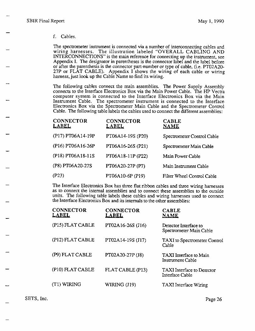
f. Cables.
The spectrometerinstrumentis connectedvia anumberof interconnectingcablesandwiring harnesses. The illustration labeled "OVERALL CABLING ANDINTERCONNECTIONS"is themainreferencefor connectingup theinstrument,seeAppendixI. Thedesignatorin parenthesesis theconnectorlabelandthelabelbeforeor aftertheparenthesisis theconnectorpart-numberor typeof cable,(i.e. PT02A20-27P or FLAT CABLE). Appendix I shows the wiring of each cable or wiringharness,just look up theCableNameto find its wiring.
The following cablesconnectthe main assemblies.The Power SupplyAssemblyconnectsto theInterfaceElectronicsBox via theMain PowerCable. TheHP Vectracomputer system is connected to the Interface Electronics Box via the MainInstrument Cable. The spectrometerinstrument is connected to the InterfaceElectronicsBox via the SpectrometerMain Cableand the SpectrometerControlCable.Thefollowing tablelabelsthecablesusedto connectthedifferentassemblies:
CONNECTOR CONNECTOR CABLE
LABEL LABEL NAME
(P17) PT06A14-19P PT06A14-19S (P20) Spectrometer Control Cable
(P16) PT06A16-26P PT06A16-26S (P21) Spectrometer Main Cable
(P18) PT06A18-11S PT06A18-11P (P22) Main Power Cable
(P8) PT06A20-27S PT06A20-27P (P7) Main Instrument Cable
(P23) PT06A10-6P (P19) Filter Wheel Control Cable
The Interface Electronics Box has three flat ribbon cables and three wiring harnessesas to connect the internal assemblies and to connect these assemblies to the outside
units. The following table labels these cables and wiring harnesses used to connectthe Interface Electronics Box and its internals to the other assemblies:
CONNECTOR CONNECTOR CABLE
LABEL LABEL NAME
(P15) FLAT CABLE PT02A16-26S (J16) Detector Interface to
Spectrometer Main Cable
(P12) FLAT CABLE PT02A14-19S (J17) TAXI to Spectrometer ControlCable
(P9) FLAT CABLE PT02A20-27P (JS) TAXI Interface to MainInstrument Cable
(P10) FLAT CABLE FLAT CABLE (P13) TAXI Interface to DetectorInterface Cable
(T 1) WIRING WIRING (J19) TAXI Interface Wiring
SETS, Inc. Page 26

SBIR Final Report May 1, 1990
(J18)WIRING WIRING (P11) (P14) DetectorInterfacePowerSupplyHarness
The Hewlett-PackardRS-20 Vectra computer systemhasa Megabyte PDMA-32circuit boardandthe Controland InterfaceElectronicscircuit board installedin theVectra'sbackplane.Thesetwo circuit boardsinterfacewith the Vectra,the Vectra'sCommunicationsPort (COM1), and the InterfaceElectronicsBox. The followingTablelabelsthecablesusedto connecttheVectratothethespectrometer:
CONNECTOR CONNECTOR CABLELABEL LABEL NAME
(P3) FLAT CABLE PT02A20-27P (J7) Control Interface to MainInstrument Cable
(P5) FLAT CABLE FLAT CABLE (J6) Serial Interface Cable
(P3) FLAT CABLE FLAT CABLE (P5) Serial Connector to Control
Interface Wiring
(P1) FLAT CABLE FLAT CABLE (P6) COM1 to Serial ConnectorCable
(P2) FLAT CABLE FLAT CABLE (P4) Control Interface to MetrabyteCable
The spectrometer has just one internal wiring harness. This wiring harness connectsthe two Omega RTD's to the Interface Electronics Box and connects the Rockwell
detector to the Interface Electronics Box. This wiring harness is labeled as "DEWAR
WIRING". See this drawing in Appendix I for these connections.
E. Software
The software for the spectrometer was developed on a 20 MHz 80386 computer running MS-DOS. The main functions of the software are:
• The control of the instrument
° Acquisition and storage of both data and status information° Display of the data and status information• Primary data analysis° Communications with other computer systems
1. Instrument Control
Control of the spectrometer is handled through the high-speed I/O board (MetraBytePDMA 32) which is directly coupled to the Spectrometer Control Board via a flat ribboncable. This gives software control of the integration time, start of data collection, controlof the filter wheel, and additional commands for later expansion. The software control ofthe instrument is handled through a set of eight commands which can be sent, with anyassociated data, to the Spectrometer Control Board. These commands are:
SETS, Inc. Page 27

SBIR FinalReport May 1, 1990
Command Description
01234567
LoadLow Byteof theIntegrationCountLoadMiddleByteof the Integration CountLoad High Byte of the Integration CountUnusedUnusedLoad Filter Wheel PositionUnused
Start Integration
The execution of any command involves a set of steps which send that command and itsassociated value to the control board and then execute that command. These steps are:
a. Set the PDMA Port A for output.
b. Load the command into the Port A register.
Co Load the command into the command register of the control board.(1) Set the AUX 1 flag.(2) Clear the AUX 1 flag.
d. If the command has a value associated with it, load that value into Port A register.
e. Execute that command.
(1) Set the AUX 2 flag.(2) Clear the AUX 2 flag.
f. Set Port A back to input mode.
Note that sending any commands during data collection would lead to undeterminedresults and could adversely affect the data collection. Under normal operations, thesoftware doesn't allow this to occur. However, if the operator inadvertently starts along integration, it can be stopped by resetting the computer system and the InterfaceElectronics Power Supply, thereby throwing away the current data collection.
2. Data Collection
The software provides the operator with several modes of data collection depending uponthe experiment and collection conditions. These modes are:
a. Average
The Average mode of data collection allows the operator to average sequential framesof data and to store the results of that average. This mode is useful when thebackground limits the integration time.
b. Difference
The Difference mode of data collection allows the operator to take the average of thedifference between successive frames. This mode is useful for continuouslyswitching between the background and the desired source.
SETS, Inc. Page 28
SBIR FinalReport May 1, 1990
c. Sum
The Summodeof datacollectionallows the operatorto takethe sumof sequentialframesof dataandstoretheaccumulatedvalueof thatsum. Thismodeis identicaltothe Average mode except it does not divide the sum by the number of framesacquired,thereforeincreasingthespeedof thedatacollection.
d. DifferenceSum
TheDifferenceSummodeof datacollectionallowstheoperatorto takethesumof thedifferencesbetweensuccessiveframesandto storetheaccumulateddifference. Thismodeis identicalto theDifferencemode exceptit doesnot divide the sumby thenumber of pairs of frames acquired, thereforeincreasing the speedof the datacollection.
e. DifferencewithWalt
The Differencewith Wait modeof datacollectionallows theoperatorto selectwhenthe sampleand referencedata is collected by using the enter key to start datacollection. This modeis usedin the laboratoryto removethe backgroundand isespeciallyusefulatroomtemperature.
All of thesemodesof datacollectioncanbeusedeitherfor acquiringsingleframesofdataor for mappingof anobject.Thedatais readinto thecomputersystemusingthehigh-speedMetraByteboardvia DMA access.Thisnominaldatatransferratesat upto 200 Kbytes/sec. Thereforeduring normal operationsa frame of data can becollectedatratesup to 2 frames/second,with theadditionaltimedueto theprocessingtimein thecomputersystem.
3. DataDisplay
a. ColorPalettes:An acquiredor previouslystoreddatafile canbedisplayedon themonitor of the computer.Themonitor is a standardVGA color monitor with 480 x640 pixel resolution,using an extendedVGA adaptorwith 512K of memory, toenablethe displayof 256 colorsat a resolutionof 480x 640 pixels. The softwareallowstheoperatorto selectthecolorpaletteusedto displaytheactivedatasetandthelinearscalingusedfor mappingthedatavaluesto color values. Currentlythe systemsupports5 colorpalettes:
(1) Rainbow: The Rainbowpalette displaysthe datavaluesusing the entirespectrumof colors.
(2) Red: TheRedpalettedisplaysthedatavaluesusingvariousintensitiesof red,with thelow datavaluesbeingblackandthehighdatavaluesbeingbrightred.
(3) Green: TheGreenpalettedisplaysthedatavaluesusingvariousintensitiesofgreen,with thelow datavaluesbeingblackandthehigh datavaluesbeingbrightgreen.
(4) Blue: The Blue palettedisplaysthedatavaluesusingvarious intensitiesofblue,with the low datavaluesbeingblackandthehigh datavaluesbeingbrightblue.
SETS,Inc. Page29

SBIRFinal Report May 1, 1990
(5) BW: The BW palettedisplaysthe datavaluesusinga gray scale,with thelow datavaluesbeingblackandthehighdatavaluesbeingbrightwhite.
b. New Palettes: New palettescanbeadded,howeverthis processwould requirecreatingbothapalettefile andaddinganewentryinto thepaletteselectionmenu.Thedatacanbestretchedin severalways:
(1) FixedScale:The FixedScaleof datastretchingallows theoperatorto entertheminimumdatavalueandthemaximumdatavalueto mapthecolor tabletoo.Datavaluesbelow theminimumgetmappedto a minimumcolor valueanddatavaluesabovethemaximumaremappedto maximumcolorvalue.
(2) Dynamic Scale: The Dynamic Scalemode determinesthe minimum andmaximumdatavalueandmapsthecolormaplinearlyoverthatentirerangeof datavalues.
c. Viewing in otherformats: Besidebeingableto displayan imageof thedata,theoperatorcanalsoview thedatain other fashionsto aid in analysis. Thesemethodsill'e:
(1) Plot: The Plot function produces a X-Y plot of any of the three axes of thedata current data set and allows the operator to specify a range in the other twoaxes to be averaged for generating the intensity data for that plot. This functionessentially provides line profile of the data.
(2) Histogram: The Histogram function produces a graph of the number ofpixels having an intensity value within a given range versus intensity. Theresulting graph is useful when setting the scale for displaying the data.
(3) Statistics: The Statistics function calculates the basic statistics on the presentdata set of a specified portion of that data set.
(4) View: The View function allows the operator to look at the actual data valuesfor each of the pixels in the present data set and to modify those values ifnecessary.
4. Data Analysis
The data analysis software allows the operator to perform mathematical operations on thedata for simple calibration data manipulation. The data analysis routines incorporated intothe software package are:
a. Add
The Add function is used to add either a constant or another data set to the current
data set. The resulting data set can then be viewed and stored on the computer.
b. Subtract
The Subtract function is used to subtract either a constant or another data set from the
current data set. The resulting data set can then be viewed and stored on thecomputer.
SETS, Inc. Page 30

SBIRFinal Report May 1, 1990
c. Multiply
The Multiply functionis usedto multiply thecurrentdatasetby eithera constantoranotherdata set. The resulting data set can then be viewed and stored on thecomputer.
d. Divide
The Divide function is usedto divide the currentdataset by either a constantoranotherdata set. The resulting data set can then be viewed and stored on thecomputer.
5. Communications
The computersystemincludesa EthernetcardandTCP/IPsoftwarefor transferringthedatasetsto othercomputersystemsfor furthermanipulationandstorage.
F. Test Results
This section discusses the tests and the results conducted on both the individual
subcomponents and the instrument as a system.
1. Spectral Range
The spectral range of the system is approximately 0.88 - 2.62 p.m. The test source is anOriel monochrometer spectrally calibrated with a Mercury low pressure pencil lamp.Argon and Krypton low pressure lamps were also employed as wavelength standards inthe NIR, e.g., Ar (1.69 & 1.37 microns) and K(2.19 & 1.8 microns).
2. Vacuum and Cold Tests
Two resistance temperature devices, RTDs, are installed in the spectrometer. RTD 1 ismounted in the detector mount, and RTD 2 is mounted on the optical bench at the rear ofthe detector assembly. Two Omega digital transmitters, mounted in the main electronicsbox, interface the temperature sensors with the Vectra's RS-232 input. The temperaturereadout was achieved by using the SCAN program in the HP Vectra's C:\OMEGAdirectory. (The program SCAN was used because at the time of testing the spectrometersoftware program did not have the existing temperature readout function.) At roomtemperature, both RTD 1 and RTD 2 read 29.2 _, and at 77cK (achieved by immersingthe RTDs in liquid nitrogen), RTD 1 reads - 194q2, while RTD 2 reads -193_.
The hold time of the spectrometer box was measured for the up-looking and side-lookingnitrogen tanks. Only one liquid nitrogen tank was frilled for each test. The RTD used tomeasure the hold time is the one mounted in the detector mount, RTD 1. The hold time ismeasured by filling the desired tank with liquid nitrogen, wait until the rate of evaporationof liquid settles (the "smoking" subsides, in about an hour), top off the tank again andstart the time counter. The RTD temperature is then sampled every five minutes and thehold time is from the start time to the time when the RTD temperature raises a degree. Inthe up-looking orientation, the hold time was about nine hours without the getter, andeleven and a half hours with the getter. In the side-looking orientation, the hold time wassix hours without the getter, and nine hours with the getter. Although the hold time for
SETS, Inc. Page 31
L
SBIR Final Report May 1, 1990
the side-looking mode is shorter, the temperature achieved in this mode is I°C lower thanthe up-looking mode: -191°C versus -190°C, as measured by the RTD. Therefore, if wedefine the hold time as the time it takes to get below -190°C for both tanks, then the holdtime for the side-looking tank increases to eleven hours. The fact that the getter made abig difference in the hold time suggests that residual gas is the main factor determining thehold time, and a good vacuum should be achieved by pumping for forty-eight hoursbefore cool down. When two to four layers of superinsulation were wrapped around thecold-shield and the liquid-nitrogen tanks, the hold time did not improve. Since there is
not enough room for more layers of superinsulation, we do not suggest usingsuperinsulation to improve the hold time. Instead, ensure a good vacuum and fill half ofthe unused tank with liquid nitrogen, as well as a full tank of the desired configuration.
The engineering grade detector (new, replacement for the delaminated engineeringdetector) has been cold cycled at SETS 19 times. This includes the cold cycle at the finalreview. No signs of degradation due to cold cycling of this detector have been observed.
3. Background and Dark Current Tests
Background and dark current were measured at the normal operating temperature of77'K. The background current measurements were made (except for 4) with the aperturewheel set at a blocked half-position and under the following conditions: (1) detectorblocked off with a cold stop and presumably "blind" to all external sources to establishthe minimum dark current value, (2) exposed to the spectrometer environment (withstray-light baffle in place) with a test aperture of the same opening as the detector activearea and without the order sorting filter, (3) same as (2) but with the current installeddetector cover plate holding the custom order sorting filter, (4) same as (3) but with theaperture wheel set at the slit aperture and (5) same as (3) but without the baffle screen.
Measurement (4) gives the background and dark current to be expected in the imagingmode. The smaller opening in the test holder of (2) (not supplied with the spectrometer)presents a smaller field of view to the detector and thus the lower derived current value
observed. A series of integration times was conducted to provide the data for the quoteddark and background current values. The background and dark current measurementswere calculated for two regions of the detector, regions A and B, to compare shorterwavelengths with longer wavelengths. Region A consists of rows (the rows andcolumns are in terms of the software nomenclature) 20-60 and columns 10--60. Columns10-60 corresponds to the wavelength region of 2.5-1.8 I.tm. Region B consists of rows75-115 and columns 75-125. Columns 75-115 corresponds to the wavelength region of1.6--0.9 gm. Table IV shows the measurement results.
Table IV. Background and Dark Current Measurements.
Measurement
(1) Detector totally blockedwith cold stop(2) Detector blocked with
small test aperture(3) Detector as in currentsetup(4) Same as 3 but with
aperture wheel at the slit position(5) Same as 3 but withoutthe baffle screen
Ibk+dcSecfi0n A (e-_ec)10
750
1040
5340
19840
Ibk+dc Section B (e-/sec)10
185
400
670
20140
SETS, Inc. Page 32
SBIRFinal Report May 1, 1990
The calculationsin "Iable IV assume that it takes 20 million electrons (fullwell of theRockwell detector) to bring the minimum intensity value of zero counts to the maximumintensity value of 4261 counts at saturation. Note, these measurements were taken with
the gain of the amplifier equal to one.
4. Intensity Resolution
The intensity resolution is determined by the 14-bit A/D converter and can be easilyimproved by replacing the A/D converter with a higher resolution A/D converter. Therange of acceptable input voltages into the A/D converter is from 0 to 10 volts. To use the
full dynamic range of the A/D converter, a variable gain is provided for the amplifier. Thedetector output voltage into the amplifier varies from approximately 0 to 3 volts. Theamplifier gain varies from approximately a factor of 3.5 to less than one. At themaximum gain, the intensity values (as displayed by the software) range from 530 to11766, and at the minimum gain, the intensity values range from 0 to 2024. Thus, theminimum dynamic range to the maximum dynamic range varies by a factor ofapproximately 5.8. (See the electronics section on more details about the gainadjustment.) For a fullwell of 20 million electrons, we then have 1700 electrons/intensitycount at the maximum gain, and 9881 electrons/intensity count at the minimum gain.Since the readout noise of the system is expected to be about 500 electrons, we will notbe able to resolve the readout noise.
G. Operation of the Spectrometer
Before operating the spectrometer, read Section II.D. 1 on care and handling of the detectorand Section II.B.2 on vacuum handling procedure. To operate the spectrometer, attach thefilter wheel-CCD camera assembly to the spectrometer, before the Interface Electronics Boxis mounted. Then, attach the Interface Electronics Box to the lid of the spectrometer box withthe four mounting screws. This brings the interface electronics to the same potential as thespectrometer (and thus the detector). Therefore, if one operates the spectrometer with theInterface Electronics Box detached from the spectrometer box, it is important to bring a leadfrom the ground wire of the interface electronics to a point on the spectrometer dewar housing(for example, one of the two ferro-motor mounts). The next step is to make sure that thepower supply is off and then remove the two circular static foam pads from the spectrometerconnectors and connect the two interconnecting cables from the Interface Electronics Box tothe spectrometer. Then, connect the power cable, main cable and filter wheel cable to the
Interface Electronics Box. Hook up the CCD camera to the video screen and a + 15V powersupply with the cables provided. Turn on the video screen and then the CCD camera powersupply. The CCD camera is very useful for rough alignment of the obiect focus on thespectrometer aperture. Connect the main cable to the HP Vectra computer and turn on thecomputer. After checking all connections, turn the electronics power on.
For room temperature operation, set the bias voltages to the following values (these are forthe Rockwell engineering detector only, since the optimal bias level for each detector is a littledifferent): LG1 = 2.0 V, LG2 = 2.2 V, IG1 = 0.4 V, IG2 = 1.5 V, VC = 6.8 V and VINV =
2.6 V. Because the dark current is so large at room temperature, the best way to detect asignal is by using the diff. wait mode of the software with an integration time of about 0.1second. For liquid nitrogen temperature operation, change IG1 to 1.11 V, and select anintegration time from 1.16 msec to 1.7 hours.
To use the spectrometer control software, type viris at the DOS command prompt. The pull-down menu driven software is relatively straightforward. Set up the desired operation mode
SETS, Inc. Page 33

SBIR Final Report May 1, 1990
by following theinstructionsin the softwaresectionor usethesoftwareHELP function. Tostartdatacollection,typeshift-F3.
If all the connections are correct and all the components are operating correctly there will bean image on the computer display. One can then continually collect data by typing shift-F3 ormodify the setup to perform other types of collection and display of data. If any problemsarise read this entire report for proper operation of the spectrometer. Remember, this is anexpensive scientific instrument and should be treated as such.
III. CONCLUSIONS and RECOMMENDATIONS
The design and operating characteristics of a groundbased imaging spectrometer have beendescribed. The instrument uses a novel approach for an imaging spectrometer. The resultantinstrument is compact and optically efficient.
Although the instrument has been sufficiently tested to determine that the design is successful, theinstrument is a prototype. Before the instrument can become a top-rate groundbased imagingspectrometer, several enhancement tasks are recommended below:
A. The grating should be replaced by one specifically made to prevent the delaminationproblem.
B. The engineering grade detector installed in the spectrometer should be replaced by thescience grade detector.
C. The horizontal line 64 is currently nonoperable and should be fixed.
D. The new elements (grating and science grade detector) should be realigned and fullycalibrated.
E. The baffle and detector cover plate should be f'me-tuned to reduce thermal backgroundcurrent.
F. The temperature sensor diode on the detector chip should be calibrated.
This instrument has significant potential due to its unique design. The instrument is especiallysuitable for commercial applications. SETS, Inc. has taken steps to commercialize the instrument,and we have high hopes for the results of this imaging spectrometer SBIR program.
VIRIS TM is a trademark of SETS Technology, Inc.
SETS, Inc. Page 34

SBIR Final Report May 1, 1990
Page Electronics Drawings Listing
1
2
3
4
5
6
7
8
9
10
11
12
13
14
15
16
17
18
19
20
21
22
23
24
25
26
27
28
Overall Cabling and Interconnections
Dewar Wiring
Spectrometer Control Cable
Spectrometer Main Cable
TAXI to Spectrometer Control Cable
Detector Interface to Spectrometer Main Cable
TAXI Interface Wiring
TAXI Interface Board J9 to T1
TAXI Interface to Detector Interface Cable
Power Supply for Interface Electronics Box
Main Power Cable
Detector Interface Power Supply Harness
Texas Instruments Camera
Filter Wheel Control Cable
TAXI Interface to Main Instrument Cable
Main Instrument Cable
New Vectra Board Layout
Control Interface to Main Instrument Cable
Serial Connector to Control Interface
Control Interface to MetraByte Cable
COM 1 to Serial Connector Cable
Serial Interface
Instructions for IBM AT Plugbord (4617 series)
Taxi Interface Electronics Layout
Detector Interface Electronics Layout
Schematic: Taxi Interface Electronics
Schematic: Detector Interface Electronics
Schematic: Control and Interface Circuit Board (2 sheets)
-- SETS, Inc. Appendix 1

SBIR Final Report May 1, 1990
SETS,Inc.
(D
(D
EoK_
O
o_O0
o¢q
O9n-
K...
O
(D
>
IX.iE
Appendix I Page I
SBIR Final Report May 1, 1990
DEWAR WIRING
TODETECTOR
PRINTED
WIRING
BOARD
3
8-"
9_
10--"
11 ._'_
12 -_'_
13"_
14 .-41--
15--'
16
TEMP
FRAME
MCLCK
YSYN
r
m_--E
ID--H
• ,..-F
I,,,- G
OD1 _vT
VDDm V
T._.. MZ)UT 1
_POD21 _ R
LG,_
LG1
IG1mE
IG2r
VC
J20
A
B
C
J21
TO
ELECTRONICS
INTERFACE
BOX
SETS, Inc. Appendix I Page 2

SBIR Final Report May 1, 1990
SPECTROMETER CONTROL CABLE
PT06A 14-19P PT06A14-19S
P17 P20
A < RED /,_/B < WHT/RED
C < BLK
D < BLK/WHT
E < GRN
F < WHT/GRN
G < WHT
H < WHTIBLK / ]
Vj < SHIELD
A
<B
<c
<.
J
SETS, Inc. Appendix I Page 3

_ SBIRFinal Report May 1, 1990
SPECTROMETER MAIN CABLE
PT06A16-26P PT06A16-26S
P16
AB
P21
M LM
NP
RS
TU
SETS, Inc.
V
Appendix I Page 4W

SBIRFinalReport May 1, 1990
TAXI to
Flat Cable
P12 1 >
o>
SPECTROMETER CONTROL CABLE
PT02A14-19S
H J17
<0
<0N/C
N/C
N/C
N/C
OM EGAD1411
V
OMEGAD1411
J17
J17
<c<o
SETS, Inc. Appendix I Page 5
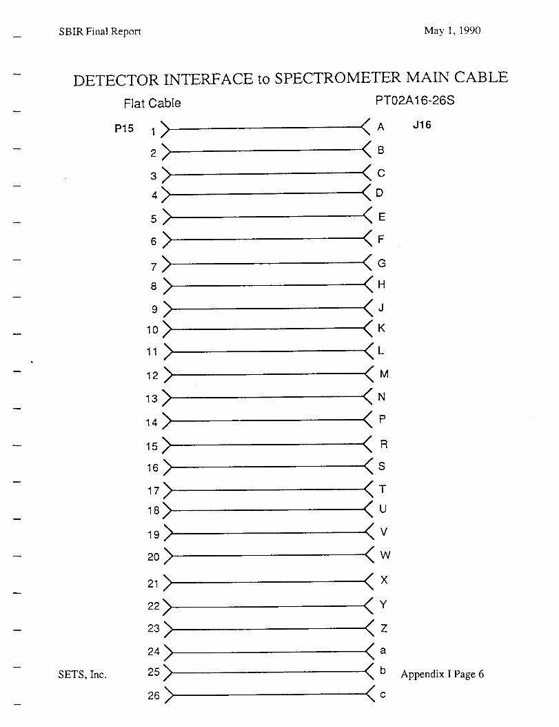
SBIR FinalReport May 1, 1990
SETS,Inc.
DETECTOR INTERFACE to SPECTROMETER MAIN CABLE
Flat Cable
P15 1> <
4> <o
,> <.
lO> <.
13> <.14> <_is> < ._6> <s
1_> <v_o> <w
_,> <a
PT02A16-26S
A J16
B
Appendix I Page 6

_ SBIRFinalReport May 1, 1990
TAXI INTERFACE WIRING
T1
1
2
3
4
5
6
7
8
9
10
11
12
13
14
15
N.C.
>N.C.
>>>>>>
NoCo
NoCo
N°Co
NoC.
NoC.
N.C.
J19 - Pin C
J19- Pin E
J19- Pin B
J19 - Pin A
RCVR - Omega
XMIT- Omega
GND - Omega
SETS, Inc. Appendix I Page 7
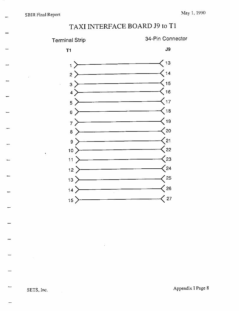
SBIRFinal Report
Terminal Strip
T1
May 1, 1990
TAXI INTERFACE BOARD J9 to T1
34-Pin Connector
J9
,> <,3
4> <,6,> <,76> <_87> <,_8> <_0
,4> <_6,,;> <_7
SETS, Inc. Appendix I Page 8

SBIR Final Report May 1, 1990
TAXI INTERFACE to DETECTOR INTERFACE CABLE
Flat Cable Flat Cable
PIO P13
1) (12) (23) (34) (45) (56) (67) (78) (89) (9
10 ) (1011 ) (1112 ) (1213 ) (1314 ) (1415 ) (1516 ) (1617 ) (1718 ) (1819 ) (1920 ) ¢2021 ) (2122 ) (2223 ) (2.324 ) (2425 ) (2526 ) (2627 ) <2728 ) ¢2829 ) 42930 ) (3031 ) (3132 ) (3233 ) (3334 ) £3435 ) (3536 ) (36
37 ) (3738 ) (3839 ) (3940 ) (40
SETS, Inc. Appendix I Page 9

SBIR Final Report May 1, 1990
POWER SUPPLY for INTERFACE ELECTRONICS BOX
J22
110 VAC
+ 18 VDCPOWERSUPPLY
+18
COM
-18
(A
<B
(C
D<
+ 5 VDC
POWERSUPPLY
+5
COM
(K
LED PILOT LIGHTW/INTERNAL RESISTOR
<L
<J
SETS, Inc. Appendix I Page 10

_ SBIR FinalReport May 1, 1990
MAIN POWER CABLE
PT06A18-11S PT06A18-11 P
P18
A
B
C
D
L
K
• j
ORN
BLK
BLK
GRN
BLK
RED
BLK
>
>
>>
>
>
/
A
B
C
D
L
K
J
P22
SETS, Inc. Appendix I Page 11

SBIR Final Report May 1, 1990
DETECTOR INTERFACE POWER SUPPLY HARNESS
PTO2A18-11P
J18 Pll
A> <1N.C.<2
N.C.< 4
P14
A> "<1
J > <3O> <'
OMEGA Transmitter
GND
+VS
SETS, Inc. Appendix I Page 12

SBIR Final Report May 1, 1990
TEXAS INSTRUMENTS CAMERA
POWER
SUPPLY
TEXASINSTRUMENTS
CAMERA
MONITOR
;-:.%::::::::::::::::::::::
:1..x g_: ::;,__: : :gz_zg:
:i_i_i/_lii!iiiiffii!ii
!_i.k.;,':i..'.:Niii/_iiiii:=i/t!i
,N.'.:,X ::::.. N'l",'k."l'
:)_..... x.:,>z,:.:,:.z.
'_NN!i#i!i!!iiii
SETS, Inc. Appendix I Page 13
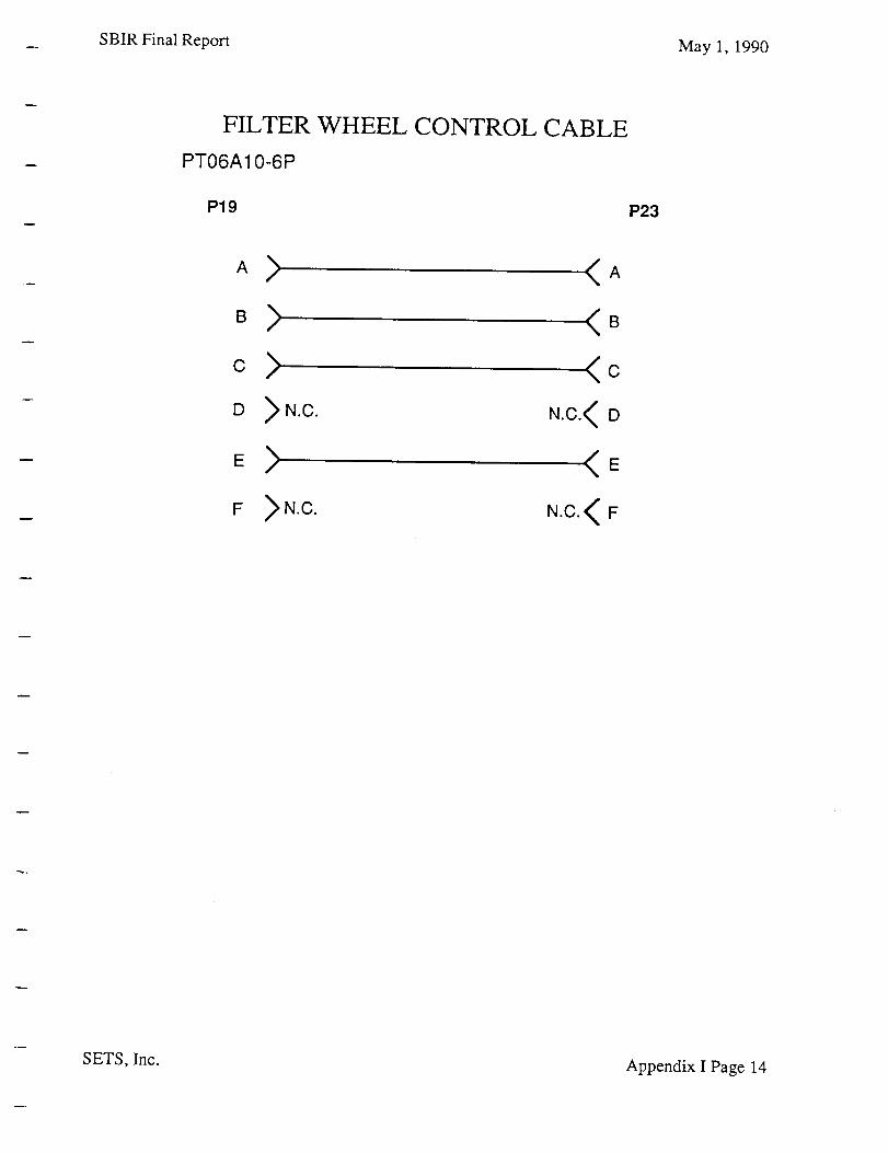
SBIR Final Report May 1, 1990
FILTER WHEEL CONTROL CABLE
PT06A10-6P
P19
c> <oD >N.C. N.C.< D
_> <_
F >N.C. N.C.< F
P23
SETS, Inc. Appendix I Page 14
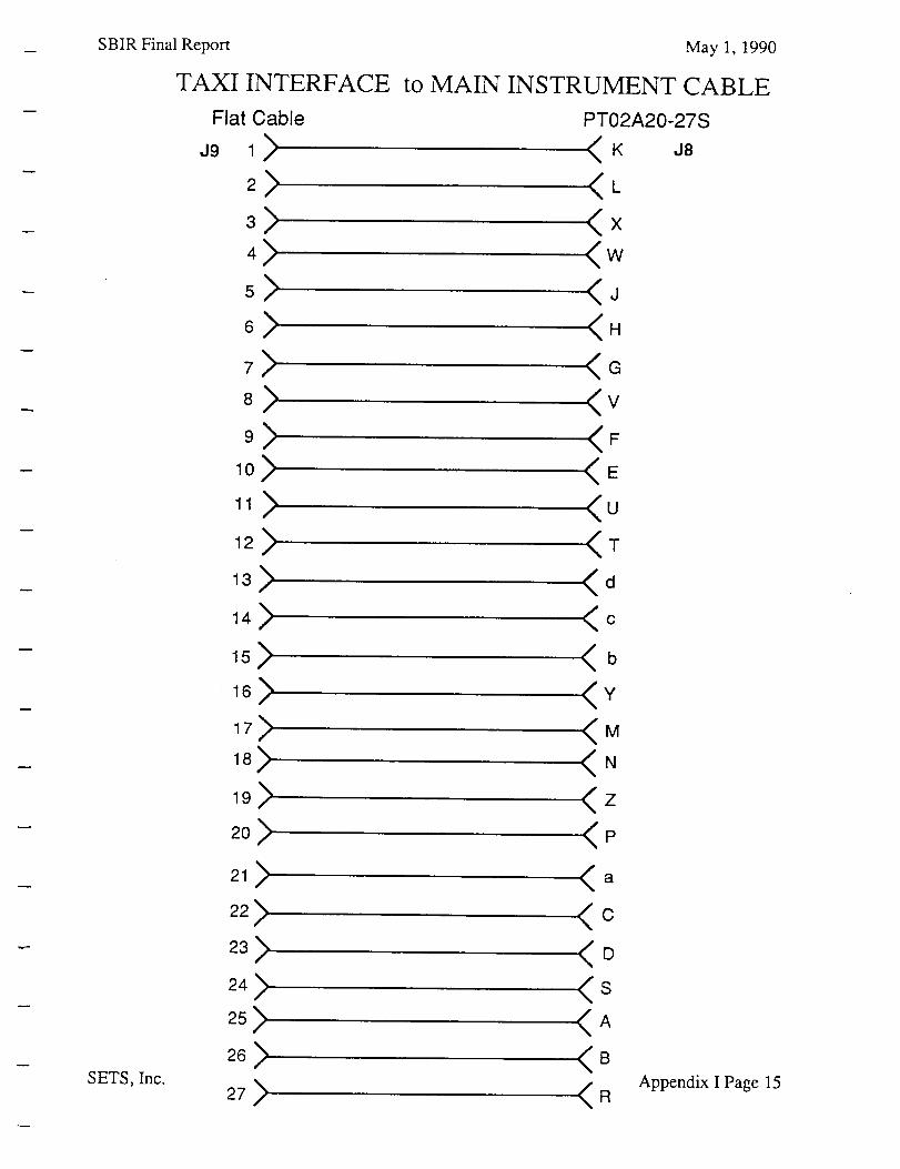
_ SBIR Final Report May 1, 1990
TAXI INTERFACE to MAIN INSTRUMENT CABLE
SETS, Nc.
Flat Cable PTO2A20-27S
J9 1> <K J8
3) <x4;> <w
8;> <_
,0;> <E,, ;> <0,_;> <7
,4;> <c
,6;> <y1_;> <.1_;> <.
_,;> < a
_';> <s
27 > < R Appendix I Page 15

SBIR Final ReportMay 1, 1990
SETS, Inc.
MAIN INSTRUMENT CABLE
PT06A20-27S PT06A20-27 P
P8 X _(_ _ X P7
L
K>JH> r_
J/ kJ
/
u \/ kJ
U
c
d
/
M \/
a \ /-,,,
"Up \/
z>J/\
D /
L
K
J
W
U
G
U
E
C
d
M
Y
P
Z
D
C
Appendix I Page I6

SBIR Final Report May 1, 1990
NEW VECTRA BOARD LAYOUT
(- a4 ")
m
U1
U7
Ull
J3
U12
U18
U19
U20
ITAXIBOARD
J
\=
1
\
m
SETS, Inc. Appendix I Page 17

S]3IR Final Report
CONTROL INTERFACE
Flat Cable
P3
SETS, Inc.
May 1, 1990
to MAIN INSTRUMENT CABLE
1
2
3
4
5
6
>>>>>>
8>
12_>
13_>
14_>
15_>
16_>
17_>18_>
19_>2o_>
21>
22_>
23_>
24_>25_>
26_>
27_>
PT02A20-27P
K J7
>,>x>,,v
>u
>t
>c
>,,>M
>P>a>o>o>s
R Appendix I Page "18

SBIR Final Report May 1, 1990
SERIAL CONNECTOR to CONTROL INTERFACE
Flat Cable Flat Cable
P3 P5
,9) <_
_'2 <'6
7
8
9
10
SETS, Inc. Appendix I Page 19

SBIR Final Report May 1, 1990
CONTROL INTERFACE to METRABYTE CABLE
Flat Cable Flat Cable
P2 P4
1) (12) (23) (34) (45) (56) (67) (78) (89) (9
10 ) (1011 ) (1112 ) (1213 ) (1314 ) (1415 ) (1516 ) (1617 ) (1718 ) (1819 ) (1920 ) (2021 ) (2122 ) ¢,2.223 ) (2324 ) (2425 ) (2526 ) (2627 ) _2728 ) (2829 ) _930 ) (3031 ) ,,'3132 ) #3233 ) _334 ) (3435 ) (3536 ) £3637 ) I"37
SETS, Inc. Appendix I Page 20

SBIR Final Report
COM1 to SERIAL CONNECTOR CABLE
Flat Cable Flat Cable
Pl P6
May 1, 1990
,> <,
3> <3
4) <4
s> <,6> (6
7> <7
8> <8
SETS, Inc. Appendix I Page 21

SBIRFinal Report May 1, 1990
Flat Cable
SERIAL INTERFACE
Flat Cable
P5 J6
1> 1
2> 2
3>
4>
3
<4
5
6
7
8
10 No connection
9
SETS, Inc. Appendix I Page 22
SBIR Final Report May 1, 1990
IN321 RE_, A INSTRUCTIONS FOR IBM * AT PLUGBORD (4617 SERIES)
1.0 BOARD DESCRIPTION
The 4617 series plugboards for the IBM AT computer have a .1 " x 1 "
hole pattern for unrestricted componenl placement. Power and
ground buses surround the grid pattern on both the component and
solder side of the board for all patterns except the 4617-4 power and
ground plane board.
The 4617.4 plugboard allows low inductance power or ground
connections to be made at any location on the .1 " x .1 "hole pattern
area with an eyelel, Vector part number T123. Push the eyelet into
the hole location to be connected, and solder the eyelet flange to the
power or ground foil.
Universal D-subminiature and .1 "x .1 * patterns are provided on the
rear board edge.
A tayoutsheet is provided to aid in I.C. and component placement.
A universal bracket is provided for tour sizes of I/O connectors or to
secure the board into the computer chassis.
2.0 CONNECTOR LOCATION AND NUMBERING
IBM motherboard connector locations are shown in fig. 2-1.
Motherboard pin numbers and signal names are shown in fig. 2-2.
IIO Pin : Signal Name
A1
A2
I A3
A4
A5
A6A7
A8
AgAIO
All
A12
A13
A14
A15
A16
A17
A18
A19
A20
A21
A22A23
A24
A25
A26
A27
A28
A29
A30
A31
-I/O CH CK
SD7
SD6
SD5
SD4
SD3
SD2
SD1
SD0
-I/O CH RDY
AEN
SA19
SA18
SA17
SA16
SA15
SA14
SA13
SA12
SA11
SA10
SA9
SA8
SA7
SA6
SA5
SA4
SA3
SA2
SA1
SAO
II0
B1
B2
B3B4
B5
: B6
B7
B8
B9
B10
Bll
B12
B13
B14
B15
B16
B17
B18
B19
B20
B21
B22
B23
B24
B25
B26
B27
B28
B29
B30
B31
Pin Signal Name
GND
RESET DRV
+5 Vdc
IRQ9
-5 Vdc
DRQ2
•12 Vdc
OWS+12 Vdc
GND
-SMEMW
-SMEMR
-lOW
-IOR
-DACK3
DRQ3
-DACK1
DRQ1
-Refresh
CLK
IRQ7
IRQ6IRQ5
IRQ4
IRQ3
-DACK2TIC
BALE
+5 VdcOSC
GND
3.0 UNIVERSAL BRACKET
A Universal bracket is provided for mounting one of 4 IIO connectors;it can also be used to secure the board without an I/O connector. See
fig. 3-1. The D-subminiature 9-pin AMP no. 745112-2; 15-pin AMP no.745113-2;25-pinAMPno. 745114.2; or 37.pin AMP no 745115-2 or
equivalent connector may be used if their dimensions match fig. 3-2to fit the bracket and computer.
• IBM is a registered trademark of International Business Machines.
"_: T E' b L
E LECTI::IONIC CDMI_ANy
SEf#_ _°dt.°neA_, Sy,=ar.CA9,342 Phooe8,8-3e_-966,
f
,";"K)P:
r:
"c,
n
I10 CHANNELCONNECTORS
REAR PANEL
;.
J.
"IL;
II
P : :
E ::
i: :1
X2 _
-, .4
E" .:,
32
l[J _
0000
FIGURE
_ _ 2-1
r
I/O Pin Signal Name
C1
C2
C3
CA
C5
O5
C7
C8
)C9
C10
Cll
C12C13
C14
C15C16C17
C18
FIGURE
2.2
SBHE
!LA23
LA22
LA21
LA20
LA19
LA18
LA17
-MEMR-MEMW
SD08
SD09
SD10
SD11
SD12
SD13
SD14
SD15
I/O Pin Signal Name
D1
D2
D3
D4
D5
D6
D7
D8
[:)9
DIO
D11
D12
D13
D14
D15
D16
D17
D18
-MEM 0S16
-I/O CS16IRQ10
IRQ11
IRQ12
IRQ15
IRQ14
-DACK0
DRQ0
-DACK5
DRQ5
-DACK6
DRQ6
-DACK7DRQ7
+5 Vdc-MASTER
GND
I FI,-,,R _ l--_;i:Pi"--'_ L .... , 1
_ = I I I_-ts.i.-.-I c ..... to, i
FIGURE I
3.2 _p_.,J.I
l J,"_$7"°"_ -- "" '=="
p¢ -- "-- Dimensions + .010"
.247":_,-_ From Eclge OfBrace To Centerline
7E x: ,0 soo-,2k: p, y

SBIR Final Report May 1, 1990
crl
SETS, Inc.
<
\
b_
l I I I t t
0 0 0 0 0 [i]!,'-h
0
_ _ F- r- -7 r-
_ _ LO _ _D II
r_
o i-r1 .'-.t_
Appendix I Page 24

SBIR FinalReport May 1, 1990
-tv
2.trl
tl)
bta"l
©
©
©
©
SETS, Inc. Appendix I Page 25

SBIRFinal Report May 1, 1990
SETS,Inc.
_.I[ t
..-.a_-...¢ o ,r
o • Kr .'
H!
I-:,;--r
---.-i;--J"
I=1
Ti
°=.u_
, I;--t
',_,"._ -..,......--+.._
I.J 2:.
IiiffJ
.--t"
[I
i: !i:; - __;_
r *_ -'¢
Appendix g 6

SBIRFinal Report
u. •
° o
• o
w
o ,.D
na
m m
N:z n
o
n
I ! '
_-----_I---
¢-------_ e.-.- °on
-" _z
"_,
g-..ir--
May 1, 1990
_n
on
l--------_b----D_
o
-_ 7_
SETS, Inc. Appendix I Page 27

SBIR FinalReport May 1, 1990
SETS,Inc.
I
i
o
I
II
_Tiiii_,
II
I-3 "l
-: _ _" I
I
I
"o_
Appendix I Page 28
ulI'-
H
U]
t---i.d
U]
m
u
m
c

SBIR Final Report May 1, 1990
o
(13
LJ -r"
H
¢.
e
c
c
! o
SETS, ,ppenct x I Page !*