DTIC Im Av 9 "fit cial-~ r, ... thankful for her cheerful encouragement and companionship. ... 2.10...
134
I~ F-- App'ove REPORT DOCUMENTATION PAGE OMI _ . 0704-0188 PjabC 'eei'.r.- b~ur~ln 'ot rt C on Of 0, etOr" eIrr-.ted to .verqe I -Ou W, w o, rW. ,Wd, u t"e tt le for revsewll nstuC IOn%. swear ct exstt; data sourmtI. galt".",rt and rarrtannq I'dt t d n d €otodC t'q nd reto rf. tht <oft,t=on Of ntorrfrao c60n S o eft" e r t bts urden t'tmr*te Of dny Oxt r * 10 v, Of ir cOfle",on 0, ,Pto . to t ,. "gnc u oq $ fon, Ore" -n tnt OruaOt to Wai,ttrqton reosuarer v. c t r, ot r r of ,or tt'On OO.a-iOr and ReDOr. 2 I efffnon Oa4- 1,9%r~a. So1e ' 204 a -to,. 'A 1120JA302 - dtO tr Onitae of Mt qeent AnM Suaget. ftoetwort RedorlO ProjeCt (07C'-0198), Watn~r9to. OC 20503 1. AGENCY USE ONLY (Leae Wn)2. REPORT DATE 3. REPORT TYPE ANO DATES COVERED 1990 Thesis x 4. TITLE AND SUBTITLE S. FUNDING NUMBERS o SECONDARY SIDE CMOS FEEDBACK CONTROI INTEGRATED CIRCUIT Ln ,AUTHOR(S) WILLIAM P. VILKINSON I PERFORMING ORGANIZATION NAME(S) AND ADDRESS(ES) 8. PERFORMING ORGANIZATION C~%1 REPORT NUMBER AFIT Student at: Massachusetts Institute of Technology AFIT/CI/CIA -90-051 I SPONSORING, MONITORING AGENCY NAME(S) AND AOORESS(ES) 10. SPONSORING" MONITORING AFIT/CI AGENCY REPORT NUMBER Wrighc-Ptatterson AFB OH 45433 11. SUPPLEMENTARY NOTES 12a. DISTRIBUTION/AVAILABILITY STATEMENT 12b. DISTRIBUTION CODE Approved for Public Release IAW AFR 190-1 Distribution Unlimited ERNEST A. HAYGOOD, Ist Lt, USAF Executive Officer, Civilian Institution Programs 13. ABSTRACT Maermurm 200 words) DTIC SELEC T EVQ 14. SUBJECT TERMS 15. NUMBER OF PAGES 1 2 16. PRICE CODE 17. SELURITY CLASSIFICATION 18. SECURITY CLASSIFICATION 19. SECURITY CLASSIFICATION 20. LIMITATION OF ABSTRACT OF REPORT OF THIS PAGE OF ABSTRACT UNCLASSIFIED I I_ NSN 7540-01-290-5500 f.Stanord ;O .'198 'u 2 991 r~j~,, ",~ S tt r." b, AN, %td t.
Transcript of DTIC Im Av 9 "fit cial-~ r, ... thankful for her cheerful encouragement and companionship. ... 2.10...

I~ F-- App'ove
REPORT DOCUMENTATION PAGE OMI _ . 0704-0188PjabC 'eei'.r.- b~ur~ln 'ot rt C on Of 0, etOr" eIrr-.ted to .verqe I -Ou W, w o, rW. ,Wd, u t"e tt le for revsewll nstuC IOn%. swear ct exstt; data sourmtI.galt".",rt and rarrtannq I'dt t d n d €otodC t'q nd reto rf. tht <oft,t=on Of ntorrfrao c60n S o eft" e r t bts urden t'tmr*te Of dny Oxt r * 10 v, Of ircOfle",on 0, ,Pto . to t ,. "gnc u oq $ fon, Ore" -n tnt OruaOt to Wai,ttrqton reosuarer v. c t r, ot r r of ,or tt'On OO.a-iOr and ReDOr. 2 I efffnon
Oa4- 1,9%r~a. So1e ' 204 a -to,. 'A 1120JA302 - dtO tr Onitae of Mt qeent AnM Suaget. ftoetwort RedorlO ProjeCt (07C'-0198), Watn~r9to. OC 20503
1. AGENCY USE ONLY (Leae Wn)2. REPORT DATE 3. REPORT TYPE ANO DATES COVERED
1990 Thesis x4. TITLE AND SUBTITLE S. FUNDING NUMBERS
o SECONDARY SIDE CMOS FEEDBACK CONTROI INTEGRATED CIRCUIT
Ln ,AUTHOR(S)
WILLIAM P. VILKINSON
I PERFORMING ORGANIZATION NAME(S) AND ADDRESS(ES) 8. PERFORMING ORGANIZATIONC~%1 REPORT NUMBERAFIT Student at: Massachusetts Institute of Technology AFIT/CI/CIA -90-051
I
SPONSORING, MONITORING AGENCY NAME(S) AND AOORESS(ES) 10. SPONSORING" MONITORING
AFIT/CI AGENCY REPORT NUMBER
Wrighc-Ptatterson AFB OH 45433
11. SUPPLEMENTARY NOTES
12a. DISTRIBUTION/AVAILABILITY STATEMENT 12b. DISTRIBUTION CODE
Approved for Public Release IAW AFR 190-1Distribution UnlimitedERNEST A. HAYGOOD, Ist Lt, USAFExecutive Officer, Civilian Institution Programs
13. ABSTRACT Maermurm 200 words)
DTICSELEC T EVQ
14. SUBJECT TERMS 15. NUMBER OF PAGES
1 216. PRICE CODE
17. SELURITY CLASSIFICATION 18. SECURITY CLASSIFICATION 19. SECURITY CLASSIFICATION 20. LIMITATION OF ABSTRACTOF REPORT OF THIS PAGE OF ABSTRACT
UNCLASSIFIED I I_NSN 7540-01-290-5500 f.Stanord ;O .'198 'u 2 991
r~j~,, ",~ S t t
r." b, AN, %td t.

Secondary Side CMOS Feedback Control
Integrated Circuit
by
William P. Wilkinson
B.S. Electrical Engineering, United States Air Force Academy
(1988)
Submitted in Partial Fulfillment
of the Requirements for the
Degree of
Master of Science
in Electrical Engineering and Computer Science
at the
Massachusetts Institute of Technology
June, 1990
Massachusetts Institute of Technology, 1990
Signature of AuthorDepartment of Electrica' Engineering and Computer Science
Certified byProfessor Martin F. Schlecht
Associate Professor, E.E.C.S. Thesis Supervisor
Accepted byProfessor Arthur C. Smith
Chairman, Departmental Committee on Graduate Students
9;: 'i3

DISCLAIMER NOTICE
THIS DOCUMENT IS BEST
QUALITY AVAILABLE. THE COPY
FURNISHED TO DTIC CONTAINED
A SIGNIFICANT NUMBER OF
PAGES WHICH DO NOT
REPRODUCE LEGIBLY.

I I
Secondary Side CIOS Feedback ControlIntegrated Circuit
by
William P. Wilkinson
Submitted to the
Department of Electrical Engineering and C-mputer Science
on May 11, 1990 in partial fulfillment of the requirements
fcr the Degree of Master of Science.
Abstract
This thesis describes the development of a CMOS secondary side feedbackcontroi integrated circuit for a power converter. The feedback controller wasdesigned for use in miniaturized point-of-load DC-DC switching power con-verters. The integrated circuit compares the output of the converter to anon-chip reference voltage and encodes the resuiting error signal on an ampli-tude modulated carrier square wave.
The circuit was designed and verified with extensive computer simulationsbefore being fabricated through the MOSIS program in the 2g, nwell CMOSprocess. Errors in the integrAted circuit layout were repaired using a FocusedIon Beam, demonstrating the beam's ability to make both connections and
detachments on integrated circuits.
The design included four major subcells, a temperature independent bandgapvoltage reference, an error amplifier, an oscillator, and an amplitude modu-lator. Subcell testing demonstrated the suitability and versatility of CMOSfor high-density power converter control circuitry.
Thesis Supervisor: Professor Martin F. Schlecht slon ?or
Title: Associate Professor of Electrical Engineering and Computer Science 0nee 3•ne 0 N
I..... ---
J;.t rt i :) den
Av 9 "fitI Im cial
-~ r,

Acknowledgements
I would first like to thank Pro.. Schlecht. His guidance and insightful ques-tions provided direction and motivated my work.
I would also like to thank the Fannie and John Hertz Foundation for spon-soring mv research. Without the financial support of a Hertz fellowship, mygrad'uate work at M I.T. would not have been possible.
I express special thanks to my fellow graduate students and colleagues ofBldg. 29 who have shared their talents with me these lst two years. I wishto thank: Andy Karanicolas for those many ',ate night sessions at the black-board; Joe Lutsky, Shujaat Nadeem, and Jeff Gross for their assistance andencouragement in the lab; Tao Tao for his willingness to attempt IC repairwith the Focused Ion Beam; and Kathy Krisch for her help in the testing ofthe FIB repair work.
I am grateful to Patrice Parris, Vince McNeil, and Curtis Tsai for draggingme out of bed in the morning and encouraging me to get some much neededexercise. I woula also like to express my appreciation toJulie Bratvold and Ray Ghanbari for their friendship and lunchtime con-versations.
I would like to thank Gee Rittenho,,se for his patieTt assistance and vatuableadvice in the laboratory. In addition to his help with my research, I alsoappreciate the times we spent pursuing our shared pastimes of computers,basketball, and sailing, especially sailing. Our catamaran adventures andBoston Harbor sailing trips were some of the most enjoyabl_ moments of mylife.
Outside of M.I.T., I would like to thank the members of Park Street ChurchChoir. Their fellowship and music provided a balance to the technical en-vironment presented by M.I.T. My three roommates and fellow Air Force
3

officers, John Ullmen, Tom Dennedy, and Todd Dierlam, deserve a specialthanks for putting up with me for th : last two years. We came as secondlieutenants, we left as first lieutenants, we must have done something right.
Of all the people who assisted m work that is culminated in this thesis, I ammost grateful to my close friend and officemate, Beerly Ford. She sharedin the day to day struggles and triumphs of my graduate study and I amthankful for her cheerful encouragement and companionship.
Finally, I would like to thank my father, mother, and sisters, Jane andMary Beth. Their faithful prayers and assistance helped me through mystudies at M.I.T and continue to uplift me in my future endeavors.
4

Contents
1 Introduction 14
1 i Feedback Controller 16
: 2 Outline ........ .............................. 18
2 Design 20
2.1 Background ....... ........................... 20
2.2 Voltage Reference ............................... 22
2 2.1 Circuit Implementation ........................ 25
2.2.2 Design Considerations .. ... .......... . 28
2.3 Oscillator .... ...... .. . . ............... 30
2.3.1 Schmitt Trigger Oscillator .... ................ 31
2,3.2 D ivider . . . .. . . . . . . . . . . . . . . 35
2.3.3 Phase Splitter ..... ............. 41
2.4 Error Amplifier ...... .......................... 44
2.4.1 Smahl signal analysis ........................ 45
2.4.2 Frequency response ......................... 49

2.4.3 Design Considerations ..... .................. 50
2.4.4 Startup Criteria ........................... 56
2.5 Modulator ....... ............................. 61
2.5.1 Circuit Implementation .... ................. 61
2.5.2 Design Considerations ..... .................. 62
3 Simulation 65
3.1 Bandgap Voltage Reference ....................... 66
3.2 Oclator ........ ............................ 70
3.2.1 Schmitt.trigger Osciator .... ............... 70
3 2.2 Divider ................................. 70
3 2.3 Phase Splitter ..... ....................... 76
3.3 Error Armpifier ...... .......................... 77
3.4 Modulator ....... ............................. 82
4 Layout 84
4. Circuit Performance ...... ....................... 85
4 1.1 Body Effect ...... ........................ 85
4.1.2 Parasitic Capacitances ..... .................. 87
4.2 Circuit Elements ...................... 89
4.2.1 Bipolar Transistors ........................ 90
4.2.2 Capacitors ............................... 92
4.2.3 Resistors ................................ 93
6

4.3 Focused Ion Beam Circuit Repair .. .. .. ... ... ... .. 94
5 Testing 102
5.1 Bandgap Voltage Reference. .. .. ... ... ... ... ... 102
5.2 Oscillator. .. .. ... ... ... .. ... .... ...... 109
5.3 Error Amplifier. .. .. .. ... .... ... ... ... .... 116
5.3.1 Folded Cascode Operational Amplifier .. .. .. .... 116
5.3.2 Analog Inverter. .. ... ... ... . .... ... 121
5 4 Modulator. .. ... ...... ..... .... ..... 123
6 Conclusion 1 25
A M.Nicrophotographs of Integrated Circuits 128
7

List of Figures
1.1 Point-of-Load Power Supply Architecture ................ 15
1.2 Switching Power Supply Topology .................... 17
2. Typical Feedback Controller Application . ............. 21
2.2 Bandgap Reference Circuit Topology .................. 23
2.3 Bandgap Voltage Reference Schematic ................ 26
2.4 Actual Current-Voltage Characteristics of an n-channel MOS-
FET ........ ................................ 29
2.5 Oscillator Block Diagramn . ................... 31
2.6 Schmitt Trigger Oscillator Block Diagram . ........ 32
2.7 Current Source Circuit ...... ...................... 32
2.8 Schmitt Trigger Topology ...... .................... 34
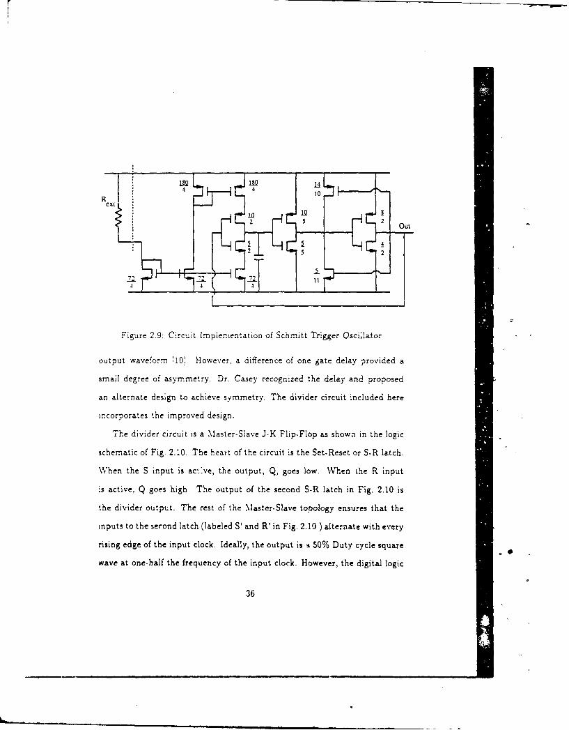
2.9 Circuit Implementation of Schmitt Trigger Oscillator ..... .. 36
2.10 Master-Slave J-K Flip-Flop ..... ................... 37
2.11 Asymmetrical Divider Output ....................... 37
2.12 NOR Gate S-R Latch ............................ 39
2.13 Scaled NAND Gate S-R Latch ....................... 40
8

2.14 Improved Master-Slave J-K Flip-Flop ................. 41
2.15 Block Diagiam of Phase Splitter ..................... 43
2.16 Phase Splitter Circuit ............................ 43
2.17 Standard CMOS Operational Amplifier Topology ......... 45
2.18 Folded Cascode Operational Amplifier ............... .. 6
2.19 Simplified Common Source Arrpiifier Circuit ............. 46
2.20 Incremental Model of Common Source Amplifier ........... 47
2.21 Cascoded Common Source Amplifier Circuit ............ 47
2.22 Incremental Model of Cascoded Common Source Amplifier 48
2.23 Small signal model used to determine output resistance . 49
2.24 Frequency Response ....... ...................... 50
2.25 Cascoded Current Mirror ...... .................... 52
2.26 Improved Cascode Current Mirror .................... 54
2.27 Experimental Folded Cascode Operational Amplifier ...... .57
2 28 Typical Error Amplifier Configuration ................ 58
2.29 Integrators with Additional Inverter Required for Startup . . . 59
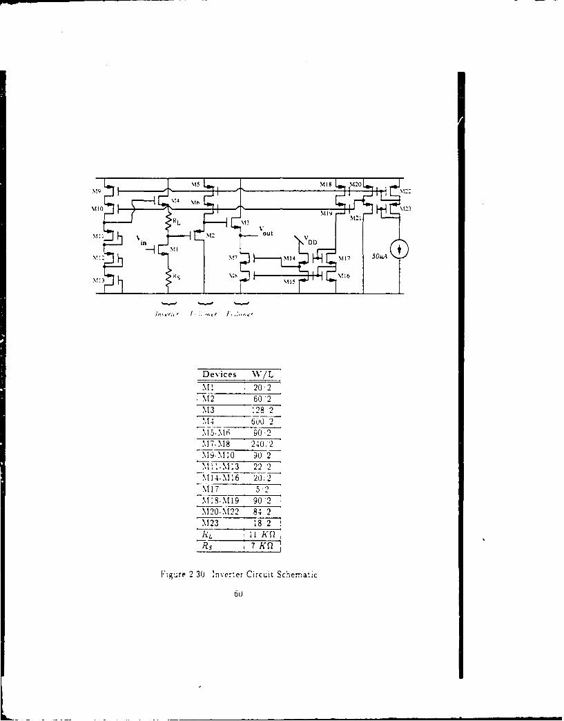
2.30 Inverter Circuit Schematic ..... .................... 60
2.31 Modulator Circuit Schematic ....................... 63
3,1 Simulated Temperature Dependence of Magic Voltage ..... .67
3.2 Simulated Frequency response of Operational Amplifier used
in Bandgap Voltage Reference ....................... 68
3.3 Simulated Temperature Dependence of Voltage Reference . . . 69
9

3.4 Schmitt Trigger HSPICE Simulatior. ... .............. 71
3.5 Simulated Schmitt-trigger Oscillator Output ............. 72
3.6 Two Gate Delay Transition .... ................... 73
3.7 One Gate Delay Transition .... ................... 74
3.8 Superimposed Transitions ...... ................... 75
3.9 Simulated Phase Splitter Output ..................... 76
3.10 Error Amplifier Simulated Frequency Response ........... 78
3.11 Inverter Simulated Frequency Response ................ 79
3.12 Simulated Frequency Response of Cascaded Operational Am-
plifier and Inverter ...... ........................ 80
3.13 Simulated Power bupply Rejection Ratio ............... 81
3.14 Simulated Modalator Output ....................... 83
4 ! Bandgap Reference Circuit ......................... 86
4.2 Error Amplifier Circuit ...................... . 87
4.3 Minimizing Drain Capaci:ance (W/L = 10/2) ........... 88
4.4 Cross.Sectional View of Parasitic Bipolar Transistor ...... .90
4 5 Scaled Bipolar Transistors ..... .................... 91
4.6 Cross-Sectional View of Capacitor Sandwich .......... 92
4.7 Trimmable Polyslicon Resistor Structures ........... 94
4.8 Layout error in the Bipolar Transistor repaired with Focused
Ion Beam Cutting ............................... 95
4., Bipolar Transistor before (top) and after (bottom) FIB repair 97
10
*1 .. ._-__d /ia mdii~ ••n

|1
4.10 I-V characteristics of Diode-connected Transistor after FIB
repair ....... . .............................. 98
4.11 Platinum Jumper Interconnect of two Parallel Aluminum lines 100
4.12 I-V characteristics of Jumper Connection ........... 101
5.1 Experimental Temperature Dependence of Untrimmed Bandgap
Circuit ....... ............................... 104
5.2 Experimental Temperature Dependence of Bandgap Circuit
with x Trimmed to 2.56 .......................... 105
5.3 Experimenta; Temperature Dependence of Bandgap Circuit
trimmed to 1.193 Magic Voltage .................... 107
5.4 Experimental Temperature Dependence of Bandgap Circuit
over Expanded Temperature Range ........... ...... 108
5.5 Schmitt-trigger Oscillator Circuit .................... 109
5.6 Experimental Results of Schmitt-trigger Oscillator ....... ... 11
5.7 Overshoot Voltage on Internal Capacitor .. ............ 112
5.8 Experimental Divider Wavefo.ms .................... 113
5.9 Experimental Divider Driven by Schmitt-trigger Gjcillator . 114
5.10 Experimental Phase Splitter Transitions ............... 115
5.11 Circuit used to Test Open Loop Gain ................. 116
5.12 Experimental Results of DC Gain Measurements ........ .117
5.13 Improved Cascode Current Mirror ................... 119
5.14 Biasing Point of Improved Cascode Current Mirror ....... 119
11

I I I
5.15 Folded Cascode Amplifier Circuit .................... 120
5.16 Input and Output Waveforms of Experimental Inverter . . . 122
A.1 Fabrication of Separate Funictional Blocks .............. 129
A.2 Fabrication of Bandgap Circuits ... ................. 130
12

List of Tables
3.1 Error Amplifier Simulation Results . ....... ........ 82
41 Foc.sed Ion Beam Milling Conditions ........... . 96
5.1 Rejection Ratio Degradation Due to Decreased Differential Gain 121
5.2 Error Amplifier Test Results . .............. 124
13

Chapter 1
Introduction
I. recv.:" years. VLSI nicroprocessirig techniques have greatlY reduced the
size Of computer logic circuits, resulting in faster, smaller computers. How-
ever, power conversion technology has not kept pace with electronic circuit
miniaturization. Computer power supplies continue to adhere to a central-
ized architecture and a low voitage d;stribution system. Consequently, the
power supp., • and disti-butior system no'." occupy as much as one-third of
the computer's total volume.
Currently, researcners at MlT are de'e'oping smaller power supplies that
would be located directvy on the computer logic boards 1o. The point-of-load
conversion arch:tecture shown in Fii 1. 1 would replace the single, large power
supply used in computers today. Since each point-of-load converter supplies
only a fraction of the computer's total power, its power handling capabilities
can be much less than a centralized power supply. Smaller power handling
requirements allow fabrication techniques which yield a higher component
14

pc board
Vac fromt andI 30-A0 VOC:
PC board
Figure 1.1: Point-of-Load Power Supply Architecture
packing density. Furthermore, once voltage regulation is accomplished at
the logic board by a point-of-load converter, the voltage on the distribution
bus can be raised. With a higher voltage, the bus can deliver the same power
at a lower current, which permits smaller distribution busswork.
In order for a point-of-load conversion architecture to be viable, the in-
dividual power modules must be very small to minimize the required space
on the computer logic boards. The largest components of the power modules
are the capacitors and inductors which provide passive filtering. In order to
reduce the size of the filtering elements while still maintaining the required
filtering, the switching fr,'quency of the module must be raised. The gains
15

achieved by raising the switching frequency and reducing the size of the fil-
tering elements are lost if the requircd control circuitry must be implemented
with numerous discrete components.Therefore, the modules' control circuitry
must be integrated on a single chip. The first prototype point-of-load con-
verters developed at MIT incorporated commercially available control chips.
However, more recent research is considering even higher switching frequen-
cies to further decrease the size of passive filter components. Consequently.
:.e c:rrent research outstrips the performance capabilities of commercial'.
availabe control IC's Not wanting to 'ose the size and performance ad-
vantages of integrated control devices, the need arises for the design and
fabrication o custo:n in'tgrated control IC's.
1.1 Feedback Controller
Figure 1.2 depicts the general topoog; of the point-of-load DC-to-DC switch-
ing power supp!ies des:gned at MIT The modules convert an input power
at 30-50 Volts DC "o an output power at 5 Volts DC. Primary side switches
produce a square-wave waveform that is applied to the primary winding of a
transformer Diodes on the secondary side then rectify this waveform to get
a DC waveform for the output. The output filter removes the unwanted AC
components of the switching frequency and delivers only the DC component
to the load. A feedback loop is closed around tne system to keep the output
voltage constant at 5 Volts regardless of changes in load conditions.
16
Isolation
Boundary
Input
PowerutOuSwitches: Trnsorer Filtput Load
PVM Coupling FeedbackCon'rol:er Element Controller
,7
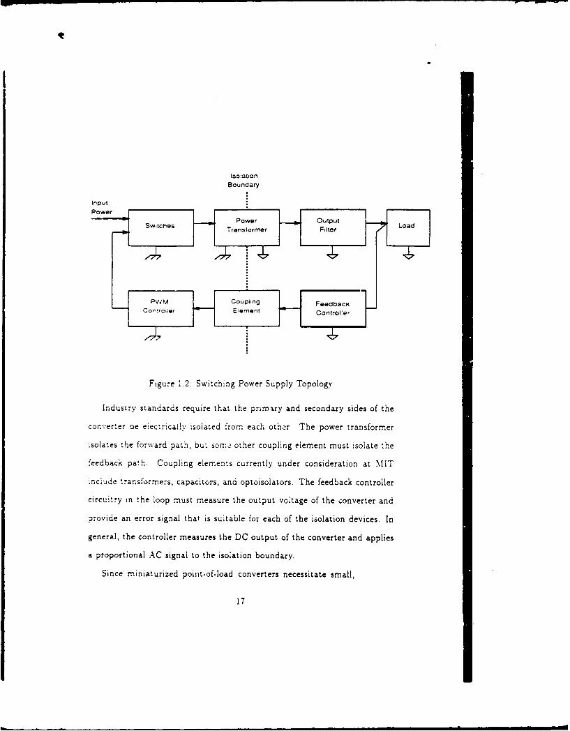
Figure 1.2: Switching Power Supply Topology
Industry standards require that the primary and secondary sides of the
converter be eiectrical!v isolated from each other. The power transformer
isolates 'he forward path, but some other coupling element must isolate the
feedback path. Coupling elements currently under consideration at MIT
include transformers, capacitors, and optoisolators. The feedback controller
circuitry in the loop must measure the output voltage of the converter and
provide an error signal that is suitable for each of the isolation devices. In
general, the controller measures the DC output of the converter and applies
a proportional AC signal to the isolation boundary.
Since miniaturized point-of-load converters necessitate small,
17

FEB-26-91 TUE 15 " FIT.-IQ L.PAFB OH P. 02
high-performanlce components, the feedback controller circuitry must be in-
'.egratcd on a single chip. The commercially available feedback controller IC's
utilize a bipolar technology. Another available technology used cxtensively
in VLSI applications is Complementary Metal Oxide Silicon, or CMOS. In
order to encourage the development of prototype IC's, the Defense Advanced
Research Projects Agency (DARPA) created the Metal Oxide Semiconduc-
tor Implementation Servicc, commonly referred to as MOSIS. MOSIS collects
designs from multiple users and then fabricates a small number of parts for
each user. Thus, by sharing the mask and wafer fabrication costs, MOSIS
can quickly producc a small nu:nber of prototype IC's for each user at about
one-tenth the normal cost. MOSIS supports primarily the CMOS technology.
Thus, given the need for custom control IC's and the availability and con-
venience of the MOSIS program, this thesis investigates the implementation
of a feedback controller in the CMOS technology. The feedback controller
provides a means to understand the capabilities and limitations of CMOS
technology for power supply control circuitry, and also affords a comparison
between CMOS control IC's and the commercially available circuits imnple.
mented in bipolar technology.
1.2 Outline
This document reports on the design, simulation, and testing of a CMOS
secondary-side feedback control IC. The next chapter presents the design
18

goals and circuit topologies chosen to meet those goals. Chapter 3 reviews
the results of HSPICE simulations ot the IC's functional sub-cells. Chap-
ter 4 addresses ,avout and fabrication concerns and presents results of some
innovative IC repeir using a focused ion beam. Chapter 5 details the per-
formance o" the circuits fabricated by MOSIS. Chapter 6 draws conclusions
about the suitabilit" of CMOS integrated circuits for power supply cnntrol
and provdes recornmendat:ons for future work.
19

Chapter 2
Design
2.1 Background
The 'unction of the control circuitry in a switching DC-to-DC power supply
.s to maintain a constant output voltage. In order to regulate the output
voltage with changes in load requirements, the converter output must be
compared to an accurate reference voltage. The resulting error voltage must
be amplified and fed back to the converter's control circuitry which will
then correct tne sensed error In this way, as the load demand changes, the
converter adapts to meet the new demand. The role of the feedback control
IC can best be understood by considering the typical example as shown in
Fig 2.1 '2.
The primary and secondary sides of the converter are electrically isolated
from each other by means of a power transformer in the forward path and
a small coupling transformer in the feedback path. The converter's 5 Volt
output is divided down and compared to an on-chip precision 1.5 Volt refer-
20

iul. Po*- rh,nd voluag
e
Relt... .... ................... !......VDD
To DmiIMrAwpiho.4e
iv
Figure 2.1: Typical Feedback Controller Application
ence. Before the error signal is applied to the amplitude modulator, it must
be inverted for startup reasons. Since the Feedback Control IC is powered
from the output voltage, when there is no output voltage (i.e. startup) the
IC cannot send a signal. Thus, zero signal from the secondary side must
correspond to the application of full power at the primary side. Hence, the
need for an inverter before the amplitude modulator. The amplitude modu-
lator receives a carrier signal from the on-chip oscillator and modulates the
amplitude of that carrier wave based on the magnitude of the error signal.
The amplitude-modulated AC signal is then transmitted across the isolation
boundary via the coupling transformer. On the primary side, the error signdl
is demodulated and utilized to make corrections to the switching duty cycles
of the converter.
21

Thus, the feedback controller IC consists of four main functional blocks: a
precision voltage reference, an error amplifier, an oscillator, and an amplitude
modulator. The design of the feedback controller investigates the suitability
of CMOS for power supply control applications while striving to achieve
design goals for each major functional block. The entire IC will be located on
the secondary side of the converter and must thus function with a single 5 volt
power supply and operate down to 4.5 Volts for proper converter startup. The
precision reference must be both temperature and supply independent. The
error amplifier must exhibit high common mode and power supply rejection
and have reasonably large gain and bandwidth. Since a high frequency carrier
signal reduces the required size of the coupling devices (transformers and
capacitors), the oscillator must generate up to a 20 MHz carrier square wave
with a 50% duty cycle. The frequency of oscillation must be externally
controllable Finally, the modulaLor must be capable of 20 MHz operation
and have a high output current driving capability. These design goals strive
to achieve in CMOS technology the performance of commercially available
bipolar IC's while inc:easing the frequency of oscillation and output driving
capabilities.
2.2 Voltage Reference
The first major component of the feedback controller is the voltage reference.
The voltage reference determines the output voltage of the entire point-of-
22

VT
Lor
IIN >', / "
Figure 2.2: Bandgap Reference Circuit Topology
load power converter. Hence, the voltage reference circuitry.must prov:de a
very stable voltage over temperature. A circuit that is to fir-t order temper-
ature independent is a bandgap reference, shown in Fig. 2.2. The bandgap
reference cancels the negative temperature coefficient of a p-n junction with
the weighted positive temperature coefficient of the thermal voltage, VT [3].
Although the CMOS process does not include bipolar devices, parasitic p-
n junctions make implementation of bandgap references possible f6]. The
output voltage is the sum of the two voltages,
V., = VBE+ KVT (2.1)
Neglecting base current, the base-emitter voltage, IBE, can be expressed
23

in terms of the bandgap voltage of silicon ext',apolated to zero degr'ees Kelvin
VBE = Vcu - VT{(- -a)I In EG] (2.2)
where V0o is the bandgap voltage, V- is the thermal voltage (N), a is the
temperature dependence of the bias current, -f is the temperature dependence
of the electron mobility, and E and G are temperature independent constants.
Substituting Eq. 2.2 into Eq. 2.1,
, = IVCo - I T(- - c,) it T -- VK(" -. In EG) (2.3)
The goal of the bandgap reference is temperature independence. Thus,
the derivative of V0/t with respect to temperature is set to zero.VTO(KV To(7 Q.
"(K - in EG) - -:° a) In To - - -,)dT 16 TOo To
which gives
(K - InEG) = (y -- a)ln To -(' - a) (2.4)
Substituting Eq. 2.4 back into the expression for V, in Eq. 2.3 results in
Vu(T) = Vco + VT (-I - a) (I + In L)(2.5)
Typically, (-y - a) = 2.2 t5i
As Eq. 2.5 shows, V.. is still a function of temperature. However, the
temperature coefficient is small and there exists one temperature where the
temperature coefficient is zero, namely To. At T = To, - = 0. The2T
24

smallest temperature dependence occurs when To corresponds to the operat-
ing temperature of the circuit. Designing to achieve first order temperature
independence at 25°C, the "magic voltage" value of Va is:
V.g(T)iT=2s.c = VGo + 2.2VTO = 1.2622 V
2.2.1 Circuit Implementation
The standard CMOS bandgap reference circuit in Fig. 2.3 cancels the nega-
tive V1 E temperature coefficient with the positive temperature coefficient of
the thermal voltage to achieve the "magic voltage" of 1.2622 volts [5j. The
circuit was designed with a magic voltage of 1.2622 in order to be temperature
independent at 25°C
The left-hand side of the circuit generates a Vr-reierenced current. Writ-
ing KVL equations around the loop as shown in Fig. 2.3
'Bs. + VGs, = VGS, + ,-V + l"BE (2.6)
The rest of the circuitry above this loop is a current mirror that ensures
that the current in the two legs are equal. Since the currents are equal,
Ts= S Vcs, and
V R = BE, - E. (2.7)
In terms of the bias current, I , Eq. 2.7 becomes
25

M5 M6 I10 M1 I
M4M20
MI5 M16
MI M2 Node A
MR2
Ige Mu Mi
n n
Devices !W/L]
M1-M4 400/3M5-MI0 900/3
MI1-M14 450/3M15-M16 100/2M17-MI8 32/2
M19 64/2M30 270/2
Figure 2.3: Bandgap Voltage Reference Schematic
26

kT I kT IIR=-In- _ -In- (2.8)
q I., q I,.
IR= kT In - (2.9)q I.,
V In_ (2.10)R
This current is mirrored to the third leg to generate the actuai voltage
.e~eren co.
- (z In n)l r (2.11)
In order to make this output voltage ternperature independent at 25°C ,
the values of n and z were calculated to set V,,, equal to 1.2622 Volts, the
"magic voltage" calculated in the previous section. A bias current of 4511A
results in a IBE = 0.5 V. Choosing n = 49 for layout convenien-e results in
x = 7 85 in order to achieve the design voltage of 1.2522 volts.
Given the temperature independent voltage of 1.2622 Volts, the op amp
follower circuit generates a temperature independent voltage of 1.5 Volts.
The resistor ratio, R2 = 5.3R 1 , insures that the 1.2622 Volts at node A
produces a final output voltage of 1.5 Volts.
27

2.2.2 Design Considerations
In additi,-r tu choosing the size ratios necessary to implement the "magic
voltage", design of the bandgap reference involves two other major consid-
erations, namely biasing and matching [71. Because the feedback control IC
is loca,ed or. the secondary side of the transformer and is hence powered by
the very 5 V signal it is regulating, startup conditions present added difficul-
ties :n biasing. In order to provide adequate control at startup, the reference
vo.age needs to operate with a power supply down to 4.5 V The large-signal
dev:ce be.'avior of a MOSFET can be approximately modeled by 8;
D'd < (,,' ) (a) (2.12)
where l is the threshold voltage, and K' is a measure of the conductivity of
the inversion layer of the device that can be expressed as
K' = o (2.13)tox
In order for transistors MI-M8 to behave properly as current mirrors, they
must be biased in the saturation or pinch-off region, with VD.S greater than
(1,s - 1v). For a given current, a larger W/L ratio facilitates a smaller value
of (1's - 1.) Hence. a !arge W "L ratio is required for devices MI-M8 to be
biased in saturation with a power supply rail down to 4.5 volts.
The second important design consideration is matching. The bandgap
circuit theory hinges on the assumption that the currents in the three cir-
cuit legs are equal. Transistor nonidealities affect this assumption. Ideally,
28

D
GS
L t' '" ... .. I
Figure 2. Ac:uai Current-Vol'age Characteristics of an n-channtl MOSFET
MOSFETs in saturation will have the same drain current for a given VCs,
regardiess of 1Vs. However, actual ID v-. Vps curves exhibit a slope that is
characterized by the Early voltage, 1,, as shown in Fig. 2.4 '91. Since not
all of the transistors in the current mirrors have the same Vs, the solution
is to set the bias at a very low Io where the slope is minimal. Ccnveniently,
low bias current also helps the 4.5 V biasing problem.
Process variations also affect current matching. Theoretically, identical
t ransistors should mirror identical currents. However, manufacturing pro-
cess variations produce non-identical transistors. The lengths of the current
mirror devices were increased to 3 microns rather than the minimum possi-
ble length of 2 microns In this way, the Wi/L ratios are less susceptible to
variations in the processing parameters.
29

2.3 Oscillator
As the high-density power conversion program at MIT strove to achieve
greater packing density at higher frequencies, the need for custom con-
troller IC's became apparent. Early researchers realized that as the program
evolved, the required control IC's would have to be developed and optimized
for each converter application. However, in order to avoid unnecessary du-
poication of IC design effort, the ear!y MIT IC designers created a library
of standard .unct:ona. buiiding blocks which could be readily included in
subsequent designs ".0'. The library, developed and pioneered primarily by
Dr. Leo Casev, contained a variety of functional circuits implemented in the
3 micron C.MOS process. However, due to the scalable nature of CMOS, the
existing circuits could be readily implemented in a 2 micron process as well.
The oscillator used in this work is a combination of standa-J an-. r, '-.
subcells drawn from Dr Casey's control circuit library. The library assrn,. d
a 10 V power supply and so it required slight modification to operate with a
5 V supply.
The internal oscillator of the feedback control IC must supply a two-phase
square wave with a 5C';% duty cvcle. Dr. Casey successfully accomplished
this task using three components from the control circuit library: a Schmitt
trigger oscillator, a divider, and a phase splitter [101. Fig. 2.5 shows his
oscillator architecture schematically. The Schmitt trigger oscillator produces
a simple square wave at twice the desired frequency. The divider divides the
30

S0hm111 Phase
Figure 2.5: Oscillator Block Diagram
frequercy of oscillation by two while insuring a 50% duty cycle. The phase
sp.:tter produces two square waves 180 degrees out of phase with each other.
2.3.1 Schmitt Trigger Oscillator
F:gure 2.6 depicts the Schmi:t trigger oscillator Initially, the Schmitt trig-
ger outiu; is a low signal and the top current source is charging the capac-
itor. When the voltage on the capacitor reaches the upper threshold of the
Scrnitt trigger, the output switches from low to high, the top current source
:s sw :tchec out and the bottom current source is switched in The bottom
source discharges th'e capacitor until the voltage on the capacitor falls below
the lo''er threshoWd of .:., Schmitt trigger and the cycle starts again. Since
tn.e value of C is f:xed ly the on-chip capacitor, the frequency of oscillation
is controcled by th- current sources.
Current Source Design
The goal of the current sources in the Schmitt trigger oscillator is to provide
a means of externally varying the frequency of oscillation. Figure 2.7 shows
31

Schmitt
T C
Fig-,re 2 6. Sc--mrt: Trigger Oscillator Block Diagram
R 100 uA
IOOuA
, 4
Figure 2 7 Current Source Circuit
32

the current source topolog. The voltage drop across the external resistor
provides a reference current that is then mirrored to the top and bottom
current sources. The external resistor provides a means to vary the current in
the current sources and directly vary the frequency of oscillation. Assuming
a 3 V diference in switching levels of the Schmitt trigger and a 400 fE
capacitor, a current of 00 IA is required for 40 MHz operation. The voltage
across the resistor and diode-connected MOSFET equals the supply voltage,
'DD = IDR- Ucs (214)
Using Eq 2 12 to eliminate V,.,
I 21DI'DD = IDR - 2 1 (! (2.15)
Choosing an exterr.al resistor of 33kQ and setting ID equal to 100,uA results
in 18 iS as shown in Fig. 2.7. The ViL of the p-channel devices reflect the
K' A P rati of approximately 2.5 which is typical of MOSIS fabrication.
Schmitt Trigger Design
As depicted 'n FIg 2 6 the current source charges or discharges the capacitor
as determined by the output of the Schmitt trigger. Figure 2.8 shows the
basic Schmitt trigger topology. The Schmitt trigger consists of two inverters
with pullup and pulldown transistors to separate the low-to.high and high-
to-low transitions. Stepping through the operation of the circuit, when the
33

P1 P2OUIN I' UT
Figure 2.8: Schmitt Trigger Topology
.npu: :s low, the output of the second inverter is also low, turning on the
pu.up cev:ce P2. Conversei., when the input is high, the output is also high,
turning on the puildown device N2. It is the pullup and pulldown devices
that sepa-ate the switching thresholds of the Schmitt trigger. Starting with
the output low and P2 on, when the input goes from low to high, Node X
cannot decrease in voltage until N1 picks up all of the current in both PI
and t.-e pul,.;) device, P2. Or. until
INI = IP1 - 'P2 (2.16)
Likewse with the output high and N2 on, when the input goes low, Node X
cannot increase in voltage unt:. the current in P1 equals that in both NI and
and the pulldown device, N2.
IIP = I'N - IN2 (2.17)
Substituting the large signal current relationships of Eq. 2.12 into Eqs. 2.16 and 2.17
results in
34

(+) N 11,g (Vc-n) 2 !i K,(DDVG )+(~P ,VDV)L 1 T L,,:,
(2.18)
( K K_1DD---';P) 2 = (2))""N K"(VDD--V' ) 2
(2.19)
Choosing s;-itching levels of 4 V and I V and assuming V;, a- _ 1V
and A' K'= 25, Ecs. 2 18 and 2.19 reduce to
"'N 1. IVP2 (.0
T~ L
P1 - 4.4 ) (2.21)
These rough sizing calculations were confirmed by a more accurate HSPICE
simulation. The ratios were similar to those developed by Dr. Casey, but,
the different power supply requirements and subsequent changes in switching
thresholds scaled the ratios slightly [101. Figure 2.9 shows the complete
Schmitt trigger oscillator.
2.3.2 Divider
The goal of the divider circuit is to obtain a completely symmetric output
signal. The divider circuit implemented in the feedback control IC is based
on a very similar divider circuit in Dr. Casey's circuit library. By a combina-
tion of digital logic circuits, the library circuit nearly attained a symmetric
35
4 4'1
Figure 2.9: Circuit Impiementation of Schmitt Trigger Oscillator
output waveform 10. However, a difference of one ate delay provided a
srail degree of asymmetry. Dr. Casey recognized the delay and proposed
an alternate design to achieve symmetry. The divider circuit included here
incorporates the improved design.
The divider circuit is a Master-Slave J-K Flip-Flop as shown in the logic
schematic of Fig. 2.10. The heart of the circuit is the Set-Reset or S.R latch.
\Vhen the S input is actve, the output, Q, goes low. When the R input
is active, Q goes high. The output of the second S-R latch in Fig. 2.10 is
the divider output. The rest of the Master-Slave topology ensures that the
inputs to the second latch (labeled S' and R' in Fig. 2.10 ) alternate with every
rising edge of the input clock. Ideally, the output is • 50% Duty cycle square
wave at one-half the frequency of the input clock. However, the digital logic
36
R mm mm m m

INOU
R Q R' R Q
Fgure ',10: Master-Slave J-K Flip-Flop
d T d T
'H L
H = T-d + d
L =T d2 i di
t H -L 2(dI - d2 )
Figure 2.11: Asymmetrical Divider Output
V. 37

circuits introduce a delay between input an output. Asymmetry is the result
of the delays as shown in Fig. 2.11. The difference in duration of a high and
low output signal is twice the difference in delays. Examining the Master-
Slave J-K Flip-Flop reveals that the delays of the final latch determine the
delays of the divider. If the delay from an S input to a low output is not the
same as the delay from an R input to a high output, the output signal will
be asymmetric.
The S-R latch originally used in Dr, Casey's divider circuit utilized a pair
of cross-coupled NOR gates as shown in Fig 2.12 '10]. Assuming an identical
dela - of d for each NOR gate, the delay from an S input to a Q output is d,
the delay through gate 1. However, the delay from a R input to a Q output
;s 2d, the delay througl' gate 2 and and the delay through gate 2. The result
is an asymmetrical output.
The improved design incorporates cross-coupled NAND gates appropri-
ately scaled to match delay times, as shown in Fig. 2.13. Assuming a
K, ,'K,' -= 2, the on-state resistance, R, of a p-channel MOSFET will be
approximately twice that of an n-channel. Thus, the delay from an R input
(active low) to a Q output is
(2R)C. 4 + (R + R)Cl,.d = 4RCI~d (2.22)
Without additional scaling, the pullup delay of an S input to a Q output
would be 2RClod. However, halving the width of the pullup transistor (as
38

R 2
S
R
JdJ djdj IdI
Figure 2.12: NOR Gate S-R Latch
39 $

s2 2LL
W WTCIoad
L
L WL
RL L
w Cload
L
wL
L wLwL
Figure 2.13: Scaled NAND Gate S-R Latch
40

OUTIN
Figure 2.14: improved laster-Slave J-K Flip-Flop
seen in Fi'z. 2.13) doubles the resistance resulting in a time delay of 4RCI .d,
balancing the delays. The improved S-R latch slightly modifies the logic
diagram of the Master-Slave J-K Flip-Flop, as shown in Fig. 2.14.
2.3.3 Phase Splitter
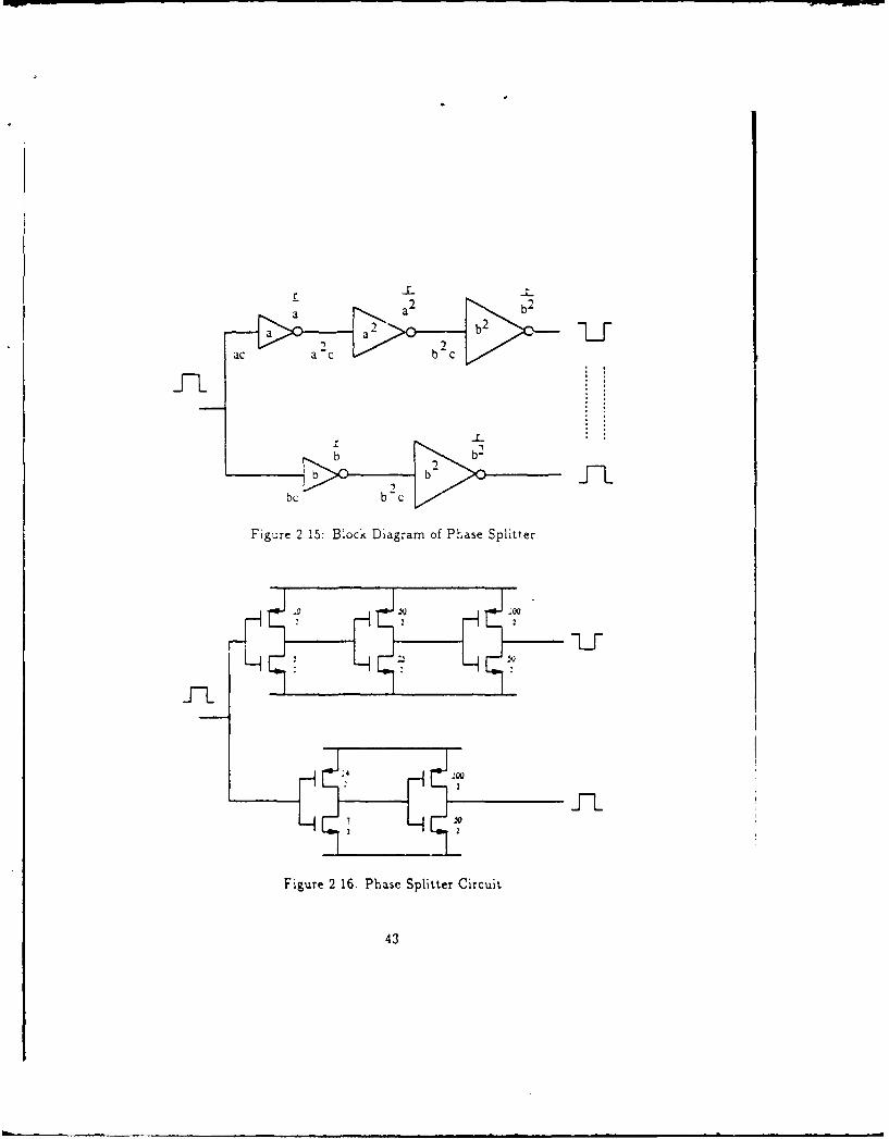
The goal of the phase splitter i; to extract two perfectly out-of-phase square
waves from a single input square wave. The block diagram of the phase
splitter is shown in Fig 2.15. Because one path has one more inverter than
the other, the two outputs are out of phase. If the delays of the two signal
paths are equal, the signals will be exactly 180 degrees out of phase. The
objective of the design was to balance the two delay paths.
The proper scaling ratios were determined by considering each unit-width
of an inverter stage to have a resistance, r, and capacitance, c. The in, erters
in the two-inverter path were scaled equally making 'he first inverter b units
41

wide and the second inverter b2 units wide. Likewise, the first two inverters
in the three-inverter path were scaled equally, a and a2 , as shown in Fig. 2.15.
In order to make the output impedance of both paths equal, the third inverter
was given a unit width of b2, as well. Given these scaling factors, Fig. 2.15
shows the input capacitance of each inverter as the product of its width and
tn'e unit capacitance, c. The output resstance is the unit resistance divided
by tke "idth.
An est:,ate of the total de;'," through each path is the sum of the RC
prod-c's o: eac% stage Eq.aturng the dla','s in the two paths .v-eds
( a2c- b2 (r) bc (2.23)
arc- ( rc= brc (2.24)
Factoring out an rc product and simpiing
a3 -a 2 b - b, = 0 (2.25)
Many pairs of numbers, (a b), satisfy Eq. 2.25. Layout design rules
dictate whole number solutions such as (4:8), (5:7), (5:18), and so on. Since
the absolute value of the time delay is proportional to the value of b, the pair
with the smallest value of b, (5:7), was chosen. The resulting phase splitter
circuit is shown in Fig. 2.16
42
r
J-FL
Figure 2 Blck6. gmo Phase Splittert
0 43

2.4 Error Amplifier
The error amplifier is s high performance operational amplifier with a mod-
erate gain and large bandwidth. The gain must be high enough to accommo-
date DC offsets in tho feedba - path. A large bandwidth gives the power sup-
ply designer flexibility in closing the feedback loop. Additionally, a primary
concern in the amplifier design is the power supply rejection. The positive
pov',Cr suppiy of the amnpl:f;lr is t-e 5 V output of the power converter-
:-.e :' signal it is measuring Thu, the amplifier must have high power
suppiy rejection. Similarly, the common mode rejection of the amplifier is
also an important design consideration The amplifier output must reflect a
difference in the input signals while rejecting common inputs.
The standard CMOS op amp as show.. Fig. 2.17 does not adequately
reject power supply noise '4. The compensation capacitor, C,, is required
to ensure closed-loop stability However, the compensation capacitor results
in poor rejection of power supply noise Ji 7 . At high frequencies, the com-
pensation capacitor 2early shurts the drain and gate of M5 together. The
'ncremental output voltage to a power supply noise signal, v., is
Av" = v, -+ AVGS. (2.26)
A constant bias current, I, dictates a constant Is, thus Avcs, 0 so that
A, =" V, (2.27)
44

VCC + vn
M 5
1~M M2
+ Cc
II 12
F~gure 2 .7 Standard CMOS Operational Amplifier Topology
and the power supply noise is coupled directly to the output signal.
An alternate op a.rp topology shown in Fig 2.18 avoids the compensation
capacitor degrada:, .",.e power s'lppl, rejection .The modified circuit
requires c' mpersat.-:. ::.cans of the load capacitor, CL, which does not
affect the power sun.:..v rcc ,n at high frequencies. This folded cascode
topology was selected for trte er.-r amplfier
2.4.1 Small signal analyik
The folded cascode topology achieves a high bandwidth by utilizing the fa-
miliar cascode configuration to overcome the Miller capacitance. The cas.
code advantage can best be demonstrated by considering the simple common
43

M9 NIO
l bias 1
M7 N181V out
"12 m I bias L
L 4 V bas
Figure 2.18 Folded Cascode Operational Amplifier
R
Figure 2 19 S=,mp.iXd Cummon Source Amrplifier Circuit
source amplifier shown in Fig 2.19 Assuming the device is biased in satura-
tion, the simplified small signal rnodei of the circuit shown in Fig. 2.20 results.
The dominant time constant associated with the gate to drain capacitance,
C~d, (also known as the Miller capacitance) is !5
TC,= Cod(Rs RL, gmRsR[L) (2 28)
However, the cascode topology shown in Fg. 2 21 decreases this time con-
46

Cgd
G D
+
Rs Vgs Cgs RL. Vgs
S
Figure 2.20: Incremental Model of Common Source Amplifier
RL
Vou
Rs
Figure 2 21. Cascoded Common Source Amplifier Circuit
stant signiF.cantv. The resulting small signal model is shown in Fig. 2.22.The
two resut ng time constants due to Cgd are
c = Cg1 (Rs - - - g, -Rs) - C,,d(2Rs) (2.29)Pri
=Co,= Cgd2(RL) (2.30)
rc, - Cgd(2Rs + R) (2.31)
47

Cgd 2
Cgs J Vgs2 R LRCgs L 2g
Rs g 2Vgs2
Cgs s 1IVgs1
Fig:re 2 22. Incremental Model of Cascoded Common Source Amplifier
The cascode configuration avoids the RLRS product, greatly reducing the
assoc:ated time constants and hence, increasing the bandwidth.
The folded cascode operational amplifier shown in Fig. 2.18 combines a
p-channel device, M1, with the n-channel device, M6, in a common base
stage to form a "folded-over" cascode stage. Similar to the common source
amp'fier of Fig 2.21, the gain of the folded cascode amplifier is 9gRL. The
load resistance, RL, is the output impedance, Ro. Figure 2.23 shows the
incremental model of MI and M6 used to determine the output impedance.
InJecting a test current, 1.,
= 1 + g,,,oVg, (2.32)
l= +1 +. (2.33)
48

ix
gM 6 vs 6 I! r°
Fgure 2.23: Small signal model used to determine output resistance
Soiving 'or z1
= (1 -gfroj? )(2.34)
The output resistance is the output voltage divided by the test current.
Solving for U
Vo = ixro, -- i ro, (2.35)
Vo = , ro, -r z,( + gnro, )r, (2.36)
Ro r , - (1 - gm ro, )ro _- g.,ro, r. (2.37)1
The gain of the amplifier is then
A,. = g jI R. :- 9., .,r ., (2.38)
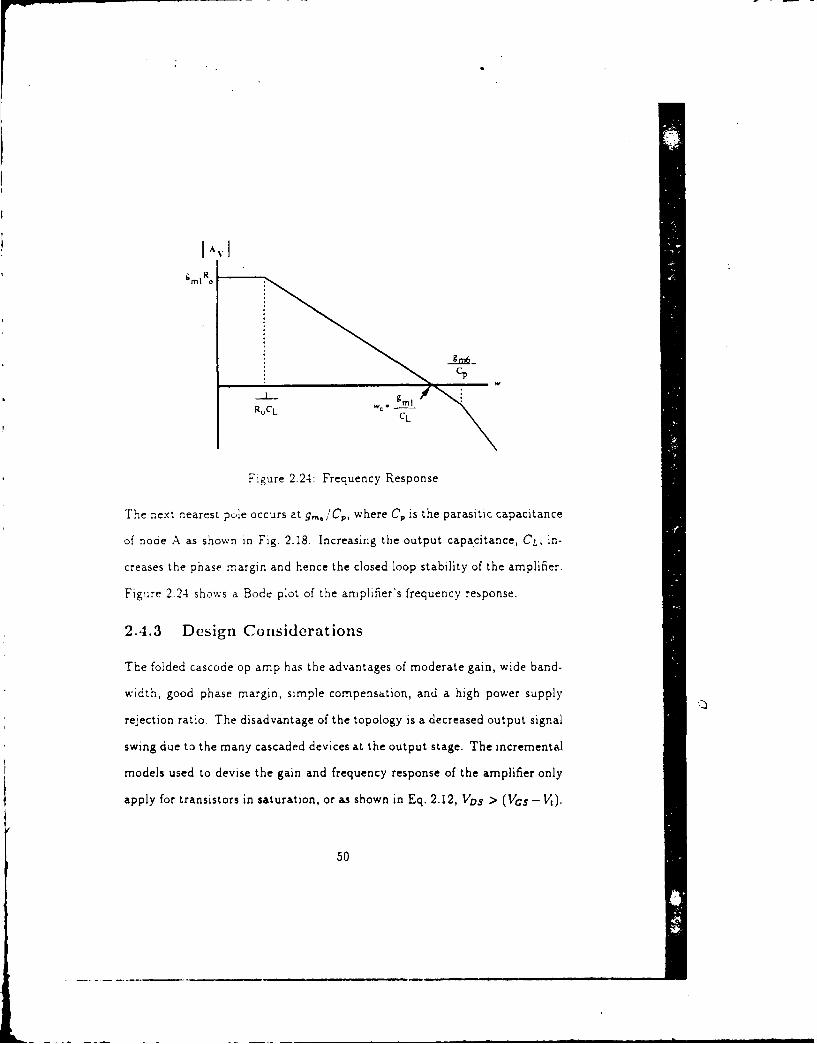
2.4.2 Frequency response
The high output impedance, R, and the compensation capacitor, CL, com-
prise the dominant time constant in the frequency resporse of the amplifier.
49
A".,
Rw
CL
9MI
Figure 2.24: Frequency Response
The next nearest pole occurs at go/Cp,, where C, is the parasitic capacitance
of node A as shown in Fig. 2.18. Increasing the output capacitance, CL, in-
creases the phase margin and hence the closed loop stability of the amplifier.
Figure 2.24 shows a Bode plot of the amplifier's frequency response.
2.4.3 Design Considerations
The folded cascode op amp has the advantages of moderate gain, wide band-
width, good phase margin, simple compensation, and a high power supply
rejection ratio. The disadvantage of the topology is a decreased output signal
swing due to the many cascaded devices at the output stage. The incremental
models used to devise the gain and frequency response of the amplifier only
apply for transistors in saturation, or as shown in Eq. 2.12, VDs > (VGS- 0.
50

Thus the output signal swing is limited by the VDS needed to keep both sides
of the output stage in saturation.
Cascode Biasing
The required V',s bias voltage needed for the current mirror load of the am-
plifier is best understood by considering the cascoded current mirror shown
in Fig. 2.25. Assuming the devices are in saturation, the drain current is
governed
1) = K( (Vs - V)2 (2.39)
In order to be in saturation, VDS > (Vs - V). Rearranging Eq. 2.39 gives
=t ID (2.40)
From Eq. 2.40, the gate to source voltage, I's is defined as
IGs = l't -- A V (2.41)
Considering the cascoded Lurrent source of Fig. 2.25, the diode connected
transistor, M1, is, by it's configuration, guaranteed to be in saturation, thus
its ls is determined by Eq. 2.41 Assuming identical curro.nt in device, M2,
the VDS needed to keep it in saturation is
VDs > V"bs - V/, (2 42)
51

Vt + AV
M 3) M4
AV
Vt + AVN NFJI \ +4 2
Figure 2,25: Cascoded Current Mirror
,DS > (I'I- AV) - V, (2.43)
IOS > A V (2.44)
Similarly, identical current and identical size means that the the VGS of device
M3 is the same as MI. or , s = (t; AV). As shown in Fig 2.25, the gate
Voltage of the top mirror is then
Vcs, - VGs, = 2(1;- AV) (2.45)
Thus, in order for device, M4, to remain in saturation
V Ds > VOS - Vt (246)
YVs > 2(l4 + AV) - AV - V (2.47)
ID S > 1 4 A AV (2.48)
52
~0 S

Combining Eq. 2.44 and Eq. 2.48, in order for both M2 and M4 to remain
in saturation, the output voltage, Vt, is limited by
V. , > V, + AV + AV = Vt + 2AV (2.49)
With a reasonably 1. rge current a typical value for AV might be .4 V. With
a threshold voltage of about a volt, V , must be no less than 1.8 volts. If the
cascoded stage is biased with a similar cascoded current mirror, the output
sng of the amplifier would be limited to only 1.4 volts with 5 volt power
supply rails. In order to achieve a larger output swing, an alternate biasing
scheme must be utilized.
Improved Cascode Biasing
The improved cascode topology is shown in .'ig. 2.26. The gate voltage of the
bottom transistors is the same as the previous topology, VGs = (V + AV).
The difference in the two biasing networks is in the sizing of M3. As shown
in Fig. 2.26, the size of M3 is W/4L. The current ir M1 and M3 is the same,
.esulting in
1 K' W 2 K'WV A I)4 2 (') 2 - 2 (v 2 )2 (2.50)
-(A 3 ) = (A )2 (2.51)4
A 3 = 2A V (2.52)
53

th sourc volag ofM4no
+2 26 (2 AV
2 + 6AV -~ V(.4
VS A V + e(2.53)
2V 3AV-Vs= , V54.4

Thus, for the improved cascode biasing network, the output signal swing is
limited by
"U, > 2-V (2.59)
The elimination on the threshold voltage by using this configuration provides
an added volt of signal s;'ing.
The inprcved cascode current source also benefits the common mode
rejection of the amplifier. If the current source that biases the differential pair
was a perfe, current s, irce, the current in .M1 and M2 would be independent
of tl-e common mode voltage. Cascoding a simple one transistor current
mirror increases the output impedance and decreases the mirror's sensitivity
to changes in common mode voltages. Using a similar improved cascode
current mirror biasing scheme for the differential current source pro':ides a
cascoded current source while still keeping the differential pair in saturation
Sizing
As can be seen from the frequency response in Fig 2.24, large values for
both g.... and g,,0 contribute to a iarge gain and increased bandwidth. The
transconductance of a MOSFET can be approximated by
= K' ID (2.60)
55

Equation 2.60 shows that increasing the bias current, ID, would increase
g.. However, as Eq. 2.38 shows, the gain is also dependent upon the output
impedance, R., which is governed by the output impedance of transistors MI
and M6. The output resistance of a MOSFET decreases with increasing bias
current as evidenced by the increased slope of ID - 111S curves of a nonidea"
MOSFET shown in Fig. 2.4. In terms of the Early voltage of the transistor,
VA, the output resistance is
I - (2.61)ID
Thus. increasing current does not necessarily increase gain. The g, of both
.M: and M6 can be increased, however, by increasing the W/L ratios. Sint-
ulation shows that the gain can be optimized with a large c.urrent in Ml, a
smaller current in M6, and large %',iL ratios for both M1 and M6. The final
amplifier circuit is shown in Fig 2.27.
2.4.4 Startup Criteria
The startup conditions require that an additional component be added to the
error amplifier. The error amplifier is generally configured as an integrator,
as shown in Fig. 2.28. As the converter is starting up, and the secondary
side feedback control IC is powering up, the 1.5 bandgap reference voltage
stabilizes before the converter output reaches 5 volts. Thus, the positive
input to the op amp will be greater than the negative input, driving the
56

NF NIsS7 I NI2 h .2..
ii ~CL
N13 I I
M17-M18Dc v i ces NV/L
.N3-NIIO 2 4 OLI2M I I-M12 270,;21M 13.M 13 80/2
_______18,2
N9.M21 84/2M22 18/2
Figure 2.27: Experimental Folded Cascode Operational Amplifier
57

V Fn'or Signal
Convcner O u!
Figure 2.2S Typical Error Amplifier Configuration
outptt ti tre posit'.:'e saturation of the op amp, since
1",l= A'(V. - V-) (2.62)
where .4, is the open loop gain of the amplifier. The very large positive
error signal is appiied to the modulator and fed back across the isolation
boundary to the pr:r.ar,' side. The primary side switch controller interprets
the high signal as an overshoot in the output and takes action to reduce the
converter output voltage, effectively shutting the converter down. Proper
startup requires that a low signal is returned when the input is below the
desired voltage. Hence, the error amplifier signal must be inverted as shown
in Fig. 2 29al.
However, the folded cascode topology of the error amplifier produces a
high-impedance output node. This is acceptable for driving the gates of suc-
cessive stages since the input impedance of a Mosfet is essenti-lly infinite.
But in order to present a low impedance output node to the user for compen-
sation purposes the output of the error ampifier must be buffered. Pushing
58

V f
(a) (b)
F.g'.re 2 2) Integrators w;t' Additional Inverter Required for Startup
t:.e :nverter into the feedback .oop as shown it, Fig. 2.29(b) provides both
the necessary buffering and inverting functions.
The three stage 1-plementation of the analog inverter is shown in Fig. 2.30.
The gain of the first stage is RL !Rs, slightly greater than one so that when
combined with the followers, the overall gain is unity. The top transistor
of the gain stage isolates the :nverter from power supply fluctuations. The
pair of followers buffer the output while nulling offset voltages. Although the
inverting stage closely resembies the common source amplifier of Fig. 2.19,
Mil:er capacitance does not significantly limit the bandwidth of the inverter
stage due to its low , and near unity gain The bandwidth limiting factor
in the error amplifier-inverter combination is the error amplifier.
59
.M5 M 8 N120
NM! 0 4 \113M19
M2 602.M3 1N122
NI n W- Iot vDD
N!I \17 M14 \1 7 ow
RS Ms5 \116
Dev ices 'N/LM. 20 2M2 60 2M3 8 22.,14 600 2M5f:; .Mt1 90,2N 17-.M8 240,2M9 -Ml 0 902M01.M23 22 2
M17 5 2M 1 -M 19 90'2M20-M22 84 2M23 18 21k. ii K 2:
iLI
Rs 7 KO
Figure 2 30 Inver:er Circuit Schematic
60

2.5 Modulator
The error amplifier compares the input signal to the bandgap reference volt-
age to produce an error signal. Based on the error signal, the modulator must
provide an AC signal which can then be applied to the isolation boundary.
To implement t-e chosen amplitude modulation scheme, the modulator must
impress tne error signa. on a carrier square wave generated by the oscillator.
To take advantage of t-e oscillator design, the modulator rrust be able to
operate vih a 2,' NIliz carrier signal. The modulator could also augment the
moderate ga:n of the amp>.4er by providing gain to the error signal. Finally,
the mod.ator should have an output swing capability of at least 2.5 volts
peak-to-peak and be able to sink and source at least 1.5 mA of current in
order to be compatible with the isolation devices (transformers, capacitors,
and optoisolators).
2.5.1 Circuit Implementation
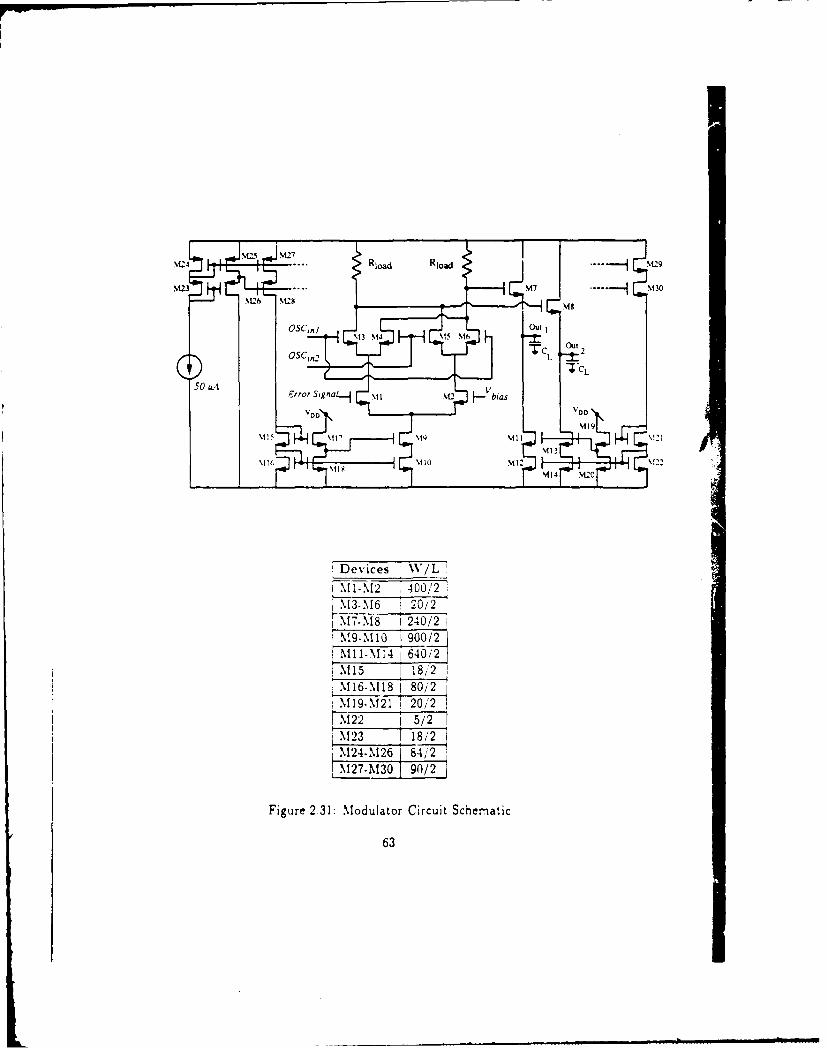
Figure 2.31 depicts the double-balanced modulator circuit. The differential
pair splits the bias current between the to legs of the modulator. The
cifference between the error amplifier operating point voltage and the bias
voltage unbalances the current in the two legs of the modulator. The cross-
coupled switches on top of the differential pair switch the currents back and
forth between the Icad resistors to produce an AC signal. Changes in the
error signal are reflected by changes in the amplitude of the signal. The
61
amplitude-modulated carrier signal is then buffered by an output stage and
provided to external pins.
2.5.2 Design Considerations
The desired 2.5 volt output swing involves trading off bias current and load
resistance. The maximum output swing occurs when one leg carries nearly
all the bias current
, = ]bo.Ri od = 2 5 (2.63)
A large resistance vaiue, R, increases the time constant associated with the
resistor and the parasitic capacitance of the node, slowing the circuit oper-
ation. A large current degrades signal swing as it decreases the range that
the differential pair remains in saturation. Utilizing the improved cascode
current source to bias the differential pair helps to widen the basing margin.
Simulation demonstrated the best results with a current of 500A and 5Kf
resistors. With large differential devices, the modulator achieves a gain of
gRL "- 16.
The load resistor and output current requirement present a tradeoff sit
uation in the sizing of the output devices. The output pads add a 5pF
capacitance to the output pins. The resistance seen by that capacitance is
1 1Rou, = - = (2.64)
9-n V4 K' TVID
Thus, increasing the W/L ratio will decrease the resistance and decrease the
62
Nt ,, , , ,27:: .
125-2R,d Rj40 M,
MI.3- 7 -.130Nub k~Ls M8
osc',,jOut
1, M.M M5 M6 out
-CL
AErrop Si9aL - II ,, bias
1113
i 191 O ! 20\1I M22 M5/
Devices \N'/LI M1 TO 0 -0,'2
%13..\ 1 20/2
VM2-M26 240/2
%l92%110 J900/2M11-M14 j 640-/2M15 1 18/, 2%116-.%18 180/M19-%121 20/2
7 2 2- 5/2
%124-%126 9 4/2
Figure 2.31: Modulator Circuit Schematic
63

associated time constant
'r= CLOAR.,, (2.65)
However, the gate capacitance of the output stage increases with size
C'9 = 2 W LCo. (2.66)
where C., = .86fF/lu2 for the MOSIS process. Ihus, increases in size in-
crease the time constant
r2 = Cqat Rloa (2.67)
Equating the two time constants prevents either time constant from domi-
nating. A sizing ratio of 240/2 results in nearly equal time constants
= .illns (2.68)
,r2 1.37ns (2.69)
The output drivers are also biased with the improved cascode current sources
to ensure that the current mirrors can sustain the high bias current and
remain in saturation.
64

Chapter 3
Simulation
The circuit topologies presented in Chapter 2 were initially derived using
rough hand calculations and first order MOSFET models. Although first or-
der calculations provided some understanding of circuit operation, they did
not provide an estimation of periormance suitable for integrated circuit de-
sign. A thorough design requires higher order models and a consideration of
the parasitic circuit elements associated with integrated circuits. Such anal-
ysis requires computer simulation. Furthermore, utilizing computer s~mula-
tion as a design tool quickly reveals how manipulating device sizes and circuit
topologies affected many different responses of the system. Thus, HSPICE, a
circuit simulator, was used to further develop the basic topologies presented
in chapter 2. HSPICE was produced by Meta-Software, Inc., and was imple-
mented on a DEC VAXstation II/GPX. MOSIS provided several HSPICE
models which characterized the devices produced by different vendors par-
ticipating in the MOSIS program. Using the typical models in the simulator,
65

the rough circuit topologies were modified and adjusted to meet the design
goals. The final schematics presented in Chapter 2 were developed via this
iterative simulation/design process. This chapter presents the results of the
simulation of these final designs.
3.1 Bandgap Voltage Reference
As previously described, the bandgap voltage reference consists of a bias
network that produces a temperature independent "magic voltage" and an
operational amplifier followe. circuit which scales that voltage to a 1.5 volt
reference ;'oltage. Both the bias network and the operational amplifier were
simulated with 1 4.5 volt power supply to ensure that the bandgap voltage
reference i5 fully operational and providing a stable reference before the power
converter reaches its final output voltage. Figure 3.1 shows the simulation
results of the magic voltage over a 0-%7C temperature range. This reference
voltage is applied to an operational amplifier voltage follower circuit. The
frequency response shown in Fig. 3.2 derronstrates that the amplifier is stable
with a 60' phase margir The operational amplifier follower circuit scales
the temperature independent voltage to produce a 1.5 volt reference. The
temperature dependence of the 1.5 volt reference voltage is shown in Fig. 3.3
Simulation results show a stable reference voltage of 1.5 V ± 1% over the
0-70*C temperature range.
66

1.3
1.29
1.28
1.27
0> 1.26
1.25
1.24
0 20 40 60 80Temperature (Celcius)
Figure 3.1. Simulated Temperature Dependence of Magic Voltage
67
*MON

80 -. 0
70 4-30
60-
-60 _
50-S
• 40 -" -90
030,
" -120
-15010b magnitude (dB)
phase (degrees)0 .."A .. J .. .. ....- 180
1 10 100 1000 1E4 1E5 1E6 1 E7Frequency (Hz)
Figure 3.2: Simulated Frequency response of Operational Amplifier used inBandgap Voltage Reference
68

1.53
1.52
o 1.51
> 1.5
0 1.49
1.480 20 40 60 80
Temperature (Celcius)
Figure 3.3. Sln.ulateo Ternperature Dependence of Voltage Reference
69

3.2 Oscillator
The Schmitt-trigger oscillator, divider, and phase splitter drawn from Dr. Casey's
library of subcefls were modified to accommodate a 5 volt power supply and
resimulated using HSPICE. Thie results closely resembled the simulations
performed by Dr. Casey.
3.2.1 Schmitt-trigger Oscillator
Figure 3.4 por:rays thre s'i:chng eve.s of the Schmitt trigger component of
tne osci'2aor. The switching threbholds of 2.9 volts for the low to high tran.
sitten and 2 volts for the high to low transition differed from the thresholds
assumed in the rough hand calculations. However, the circuit still exhibited
the Schmitt trigger behavior necessaiy for oscillator operation as demon.
strt.ed in the simuiation results of the Schmitt-trigger oscil!ator shown in
Fig 3 5. The duty cycle of the square wave was unimportant because the
divider circutr;" triggers off the rising edge of the signal produced by the
Schmitt-trigger oscillator
3.2.2 Divider
The divider c:rcuit incorporated an improvement over the the divider cir-
cu;t used by Dr Casey The divider utilize. a scaled NAND gate S-R latch
rather than a NOR gate latch Figur- 3 7 shows the high-to-low transi-
tion of the output in response to a RESET input command The RESET
70

4-43
0.
a--
CnC
0 1 2 3 4 5Schmitt Trigger Input (Volts)
Figure 3 4; Schmitt Trigger lISP ICE Simulation
transi on involved two gate delays from input to output. Figure 36 shows
the low-to-high transition of the latch output corresponding to a SET input
command The SET com mand oct~vated the output with only a sing!V gate
delay. However, the gate delay was increased to match the two ga-te delays
of the RESET command by scaling the transistor widths. The two outputs
are superimposed in Fig 3.S, ditplaying crossover at 2.5 volts for a 507-c duty
cycle
71

5-
4
- 3 -
- 2 -0
0. 0Co 2
U
-1 , . . 1 . . . . .
20 30 40 50 60Time (nanoseconds)
Figure 3 5: Simuiated Schmitt-trigger Oscillator Output
72

5r
4-
0> 3-
2-0M1
0- - - - Input
-- Output-I.1 I I
0 5 10 15 20 25 30Time (nanoseconds)
F;gure 3 6 Two Gae Deiay Transition
73

- -- - -- - -
4-
|0
> ~3-
20
1ICI
0 - -- - -- - -- -
cC
InputOutput
-1I I I
0 5 10 15 20 25 30Time (nanoseconds)
Figure 3 7. One Gate Delay Transition
74

5
4-
3-
2-
00
0 5 10 15 20 25 30Time (nanoseconds)
F~ge 3 S Super~m,.)-sbd Tranbitlon's
75

6
5
4
3-
0 2-
CLC
0.0
0 5 10 15 20 25 30 35 40 45 50Time (nanoseconds)
-.g.re 3.9 Si:nu'ated Phase Splitter Output
3.2.3 P ha.c Splitter
The phase spl:ter produced two uut of phase square waves from a single
square wave input. The two outputs are shown superimposed in Fig. 3.9.
The s;mulated waveforms exibibted an acceptable delay of 0.5 ns.
76

3.3 Error Amplifier
The error amplifier design strove to achieve a high bandwidth with moderate
DC gain, as well as high power supply and common mode rejection ratios.
The small signal analysis of the amplifier resulted in a DC gain of
.4, = g,, Ro = (903 -7 )(2.54 Af Q) = 2,294 (3.1)
The 'ow frequency pole occurred at
P= (I1~ () = 10 kHz (3.2)
resulting a unity gain crossover frequency of
f, = ( I ) = 23.2 MHz (3.3)
Layout techniques minimized the parasitic capacitance which dominated
the next significant pole,; = g,.iCP, resulting in a phase margin of 90
degrees. The Bode diagram of Fig. 3.10 summazizes the frequency response
simulation of the t rror implifier.
In order to preserve the high frequency characteristics of the opera-
tional amplifier, the analog inverter required for startup needed a bandwidth
'hat exceeded that cf the error amplifier. The simulation results shown in
Fig. 3.11 show how the inverter achieves unity gain inversion with a unity
gain crossover frequency a decade above the operational amplifier.
77

80 0
70-
0 -60 0400
20-
10- magnitude (dB)---- phase (degrees) '~-120
1 10 100 1000 1E4 1ES 1E6 1E7 lEBFrequency (Hz)
Figure 3 '0: Error Amplifier Simulated Frequency Response
78

2 .0 111I,180
, - 210
o
0 240 A
' 270
- magn!tude (Volts)----- phase (degrees)
0 -- j ." j ... J 3001 10 100 1000 1E4 1E5 1E6 1E7 1E8 1Eg1E1OFrequency (Hz)
Figure 3.11: Inverter Simulated Frequency Response
79

80 0
70"
-3060-
"50 -60" 40
30 " - ---
20 .120
10_ magnitude (dB)phase (degrees)
I0 -1-J ....J ..... 'J 1...... J . . I .. -J . . . 1501 10 100 1000 1E4 !E5 1E6 1E7 1E8
Frequency (Hz)
Figure 3.12: Simulated Frequency Response of Cascaded Operational Am-plifier and Inverter
Cascading the inverter and operational amplifier produced the frequency
response shown in Fig. 3.12. The operational amplifier limited the bandwidth
while the inverter decreased the phase margin by 30 degrees.
Figure 3.13 shows the power supply rejection ratio of the error amplifier
as a function of frequency. The power supply rejection ratio is defined as f11]
PSRR Ap (3.4)AP
80

80
70-
00, 50-
" 40-
S 3o-
2o-
10"Cl
1 10 100 1000 1E4 1E5 1E6 1E7 1E8Frequency (Hz)
F'Z:gre 3,13: Simulated Power Supply Rejection Ratio
where AD is the armplifiers differential gain and Ap is the ratio of the response
at the armpifier output to a signal on the power supply rail. Thus the PSRR
of the error amplifier decreases with frequency as shown in Fig. 3.13
The remaining simulation results of the error amplifier are summarized
in Table 3.1.
81

Parameter I Test Condition unitsInput Offset Voltage V, , = i.5V 0.238 mVInput Bias Current 1,, = 1.5V 0 a.AInput Offset Current V,, = 1.5V 0 MASmall Signal Open Loop Gain 68 dBCMRR V,, I - 3.5 V 98 dBPSRR DC 69 dBOutput Swing 1.5 VMax Sink Current 500 uAMax Source Current 5 mA
Unity Gain Bandwidth 23 MHz
Table 3.1: Error Amplifier Simulation Results
3.4 Modulator
The complete simulation of the modulator combined a1 of the feedback gen-
erator elements. The error amplifier input to the modulator was a 0.4 V,,-,
I MHz sine wave. The 20 MHz carrier wave was supplied from the phase
splitter outputs. The moduiator outputs were driving 5 pF load capacitances
to simulate the capacitance of the IC bonding pad Figure 3.14 shows the
simulation results of the modulator output.
8?

4h
0 2-
0 100 200 300 400 500 600Time (nanoseconds)
Figure 3 1.1 Simulated Modulator Output
83

Chapter 4
Layout
B'c ,re ,'-e feedback contr J.xr circuitry could be submitted to MOSIS for
fabrication, the pnh s c- arrangement and implementation of "he circuit ele-
ments had to be deined by means of an integrated circuit layout. Although
this chapter addresses the layout separately, layout considerations were an
integral part of the dcesignsmu..:.on process. In addition to modeling the
device parameters of :'pca .OSIS fabrication facilities, IISPICE also sim-
• .ata the cffects of d,7- ren 1a:.'out geometries and device placement This
chapter addresses layout-dependcrnt abpects of circuit performance Trans.
lat:ng the simulated circuits into an integrated circuit mask al. ; involved
ac' ; :.g s,"~.,, features c., the :IOSIS fabrication process. The M')SIS pro-
ce.,s ;s ta:',,red to accornrodate CMOS digital logic circuits. This chapter
discusses the adaptations requ,:red to utihze the MOSIS facility fo analog in-
tegrated circuit design Finally, the fabricated circuits receved from MOSIS
contained a layout error which was repaired using an innovative applh tion
84

of a Focused Ion Beam (FIB). Repair work on the feedback controller IC
demonstrated the suitability of the FIB for both detaching and connecting
metal lines on integrated circuits.
4.1 Circuit Performance
4.1.1 Body Effect
In The .,OS IS:n- ,e' proce,. :.e i.-ci.an:.vi transist,,rs are fabricated d:-
rect.. on t'e p-tve substra:e. w .v t.e p-channel cevices are p'aced n n-
,vpe wei-s T -ek or we.l subtrate vot-Age directly :mpacts the threshoid
voltage of the MOSFET The threshold voltage is defined as '8
= ;- - (Vs)' 3 (4.1)
where Vsj :s the source to buk voltage, 1 o is the zero bias threshold voltage
and I is a constant wh:ch depends upon processing parameters such as the
doping concentrations and the ox.de thickness. Typically, -r = 0.5 for MOSIS
fabrication processes
The increased threshoWd ,'.nae due to the bdy effect greatly impacts the
biasing of the baigap ,,.':. c;7cuit sE:)wn in F:g 4 1. The bodv effect
increases the thresliuid v,,tages of .M1-.MS which increases the required rail
voltage necessary to bias the current M.irrors. However, the body effect for
the p-devices MS-MS was eli inated by placing those devices in separate
wells and tying Ole source of each transistor to the well.
85

SIII
\.cA
F gu:re 4 Bandgap Rf ference Cl"cuit
86

'biias
Figure 4 2. Error Arnp>fer Circuit
4.1.2 Parasitic Capacitances
The MOSFET source and drain diffusions g:ve rise to junction-depletion ca-
pacitanceswiichdi:rectlyimnpactperfoimnce As was shown in Section 2,4.2,
the sec-..d do0:7nant pce of the ?!rr ampliFer is determined by 9, 'Cp,
where CP :s the paraslt:c capacitance of Node A, as shown in Fig. 4 2 In.
creasing the bdndwidth of the arnp,;Fier equates to pushing the secondary
pc,,e out tu higher frequenc;es Thus, the drar,-to.bulk parasitic capacitance
of transistors MI and M4, and the source-to-bulk parasitic capacitance of
tra isistor M6. decrease the bandwidth of tht amplifier. A transistor-folding
layout technique can decrease the parasitic junction-depletion capacitance
without decreasing the W!L ra':os of the devices.
The sourre and drain diffasion areas form a p-n junction with the sub.
87
a

4 ORC ]DALI ransistur A T ransistor B
Figure 4 3 MmInmzing Drain Capacitance (W/ L = 10,2)
s r at e The s'.des of th~e diffrusion and the bottom area of the diffusion al"
cor.:r;bute to th. e para-;Lic 2 urnclion capacitarce. Thus the capacitance to
th-e S.;su .-tr e .:,r ''e dramn is
C' -C,;.ra~ of but.um, - C,.,(Peri7riacr) (4.2,
wreC, is the 'U ru :1- ulk "uniction caipac~tarnce and C,,~, is the side-wail
per:pher. capacitance T-,p:cal M.OS!S parameters are
C, = 0.29 fF/jim (4.3)
Cjw=0.34 fF,'jum (4 4)
Thus, to ninimize parasitic capacitauices the :avout should minimize drain
or source perimeter and area Figure 4.3 sh~ows two transistors, both with
88

W/L ratios of 10.2. Transistor A has a drain and source area of 60 'm2
and a perimeter of 22 pm. Transistor B has a source area of 60 Aim' and
a source perimeter of 34 Mm. However, the drain of Transistor B has an
area of 30 uim 2 and a perimeter of 12 um. Thus the drain-to-bulk capaci-
tance of Transistor B is approximately half that of Transistor A. Although
the snoirce-.o bu:k capacitance is significantly higher, the added capacitance
is placed v.ere it :s uni mpc.rtant to the circuit. For instance, in the error
a- p lc tc dra n capacitance of transistor M- is mmim:zed, the source
'pac::.ance :s ;ncreastd. Hov.ever, add*iona: srurce capacitance only adds
capac~tance to the ground node where it will not affect circuit performance
Similarly, minimizing the source capacitance of transistor M6 significantly
increases the drain caoacitance. But, such ar. increase only adds capacitance
to the output node where it simply adds to the compensation capacitor. The
same arrangement applies to the input differential pair as well. Through-
out the lavut, capacitance was minimized on critical nodes and shifted to
unimportant nodes by proper fo'ding of the devices.
4.2 Circuit Elements
I he circuits presented in Chapter 2 were implemented in the MOSIS 2.
inicron, n-well process. The nanufarturing process was designed to accom-
modate CMOS digital logic circuits. There:ore, several circit elements re-
quired for analog circuit design, namely bipolar transistors, capacitors, and
89

Collector Base Emitter
ni-Aell N
p-type substrate
Figure 4.4: Cross-Sectional View of Parasitic Bipolar Transistor
resistors, were deve'o.ed from the available mask layers.
4.2.1 Bipolar Transistors
The bandgap reference circuit shown in Fig 4.1 required bipolar transistors
with area ratios scaled 1:49 Although the CMOS process offered by MO-
SIS dues not provide bipolar devices, the technology contains an inherent
p-n-p transistor A p-diFusion in an n-well in the p-substrate produces a
parasitic p-n-p structure, as shovwn in Fig. 4.4. A single emitter diffusion
of 10urm x 10,.im was uti..ze-d for the unity size transistor. The scaled tran-
sistor was impteme:ited with forty.nmne 10pm x 10,um emitters diffused into
a single well. The two bipo'ar structures are shown in Fig. 4.5. The well
contacts around the edge of the emitter array formed the base contact and
the substrate contacts around the edges of the well provided the collector
contact
90

Figurr' S -ii i Bliar Trarmsts-rs

Metal 2
Metal I1N l
Substr.ate
Figure 4.6i Cross-Secticnal View of Capacitor Sandwich
4.2.2 Capacitors
The error arnn.;::er and the operationa: amplifier in the bzndgap reference
circu:- required compensation capacitors to insure stability. The current
source in the osciijiator circuit charged and discharged a capacitor to trigger
the Schmitt trigger. These capacitors were fabricated by utilizing parasitic
capacitances inherent in the MOSIS process. The capacitance between the
two mctal iayers was approximately .049fF;'pm' while the capacitance be-
tween metal I and the substrate or we!l was approximately 0.026fF/ m 2.
Sandwiching a metal I layer between a metal 2 laver and the substrate cre-
al ed a structure that had a capacitance of apprc .imately O.075fF/lim'. Fig-
ure 4.6 depicts the capacitor sandwich structure. Thus, the .,: ar;,nlier's
6 pF cumpensation capacitor requir.-d a capacitor structure of approximately
285ym x 285/um. When one terminal of the capacitor is grounded, the sub-
strate furms the bottom plate of the capacitor. When neither terminals are
groinded, an n-we!l forms the bottom layer.
After the circuitry presented in this thesis was fabricated, MOSIS offered
92

a new double-poly process. Using this new process, capacitors can be eas-
ily fabt,cated by overlapping the two layers of polysilicon. The polysillcon
capacitors also provide a much higher capacitance per unit area.
4.2.3 Resistors
The resistors were implemented in polysilicon. Typical values of polysilicon
sheet resistance vary frorm 20-40 ohms/square, depending on the particular
vendor per..:ni'g the fabrication for MOSIS. Thus, whenever possible, cir-
c,'.;s were r-es'gned to operate on resistor ratios, not absolute values. For
.nstance, in the bandgap circuit shown in Fig. 4.1, the temperatilre indepen-
dent voltage is dependent upon the ratio of resistors, z, not the particular
resistor values. To facilitate matching in the resistor ratios, the smaller re-
sistor was laid out in a reproducible geometic shape and the larger resistor
consisted of multiples of that shape. In addition, a binaiy-weighted resistor
trimming ladder was added to the end of each resistor. Before trimming,
metal 2 shorts out the entire trimming ladder. The metal 2 lines formed
jumper wires that can b! broken with a probe to add binary-weighted incre-
mrents of resistance to the existing resistor. For instance, to add an additional
20 squares of resistance, the jumpers shorting out sections of 16 and 4 squares
can be removed. However, in some instances, particularly the modulator, an
absolute resistance value is desired. In this case, the resistor layout assumes
a typical value of 23 ohms/square with a large enough trimming structure to
accommodate resistance variations of 20-40 ohms/square. Figure 4.7 shows
r 93
,L ... I

I0
I. gure I T I'rirnrnable Pok ysilicon Resistor Structures
at i"d polysi I icon rpsIs to rs at I t Ieiv r bi n a r we ighI ted tri Im mIng lad d ers.
4.3 FocLused Ion Beam Circuit Rep-air
'Ihe~ original mask submitted to M~OSIS contained a layout crror in the
linrdga p referenice circuit. SpecificallY, the co)llector, base, and eitter of
the -;:iglr.TT mitter or unity-sized hr polar transistor were shorted to ground,
rrndering the circuit inoperable. As shown in the bandgap1 SChemIIatic in
Fig I I , thei hase arid colh'etor of the diode-ronnert ,fl t rai~sistor werr con-
nect t'd to ground. H owever, the laYout e-rror also shorted the rm ~it, t-

Desired Cuuing Phaes To Bandgap Bias. Network
Collector
~oxide
Base
ELtii " Con,.act Me:. ayoutE -~Metal 2
Figure 4.8: Layout error in the Bipolar Transistor repaired with Focused IonBeam Cutting
ground. Figure 4.8 depicts the layout error. A metal 1 layer connected the
emitter contact to the rest of the bandgap circuitry. However, t.ie metal 1
base lead crossed the emitter lead, shorting together the emitter, base, and
collector. Fortunately, the base and collector terminals were connected to
ground via other connections on both sides of the emitter lead. Thus, the
circuit could be repaired by making two cuts, one on either side of the emitter
lead as shown in Fig. 4.8
The microsurgery was performed at MIT by Tao Tao using the SIM 50
Focused Ion Beam. The SIM 50 utilizes Gallium for its liquid metal ion
source. The operating conditions during the milling are shown in Table 4.1.
Figure 4.9 shows the area before and after the milling. Before the cutting,
the device exhibited short-circuit characteristics. After the cutting, the diode
95

Operating ConditionsGallium ion energy 30 keVIon Current 140-240 pAMilling Time 30 min.Ion Beam scan rate 3.7 kHz
Table 4.1: Focused ion Beam Milling Conditions
cornected transistor exhibited the typical diode I-V characteristics as shown
In Fig. 4.10. The apparent low breakdown voltage for negative voltages is due
to the substrate-source p-n junction of transistor Mi of the bandgap circuit.
This substrate-source diode turns on when the test voltage falls less than -0.6
volts. However, the forward L'ias condition demonstrates the siaccpss of the
FI3 repair.
The success of the FIB cutting operation led to further investigation of
integrated circuit repair. The focused ion beam is capable of metal deposi-
tion as w~il as milling. Previous work had demonstrated the feasibility of
connecting two levels of metal at an intersection [12] . This work was re-
peated, connecting two crossing aluminum hies by milling a hole through
both lines and depositing p itinum into the hole. The connection had a re-
sistarce of 5Q and withstood a maximum current cf 100 mA. The deposition
demonstrated the Focused Ion Beam's capability of connection as well as
cutting in integrated rircuit repair. However, layout repairs do not always
involve connection J overlapping metai iayers. Often metal lines of the same
level need connecting. Thus, another application was pursued using samples
96

V
Figfire 4.9: Bipolar Transistor before (top) and after (bottomi) FIB repair
97

ki+ F VTPQP MOaSurad
It
- . /"' .1.
-- 0 4" 0
Figure 4.10: IV characteristics of Diode-connected Transistor after FIB re-pair
98

of the feedback controller IC. The third application considered connecting
parallel metal lines with a jumper wire of deposited platinum. The con-
nection is shown in Fig. 4.11. Two parallel metal lines, 10 Am apart, were
connected by a FIB-deposited jumper wire. First the FIB was used to mill
a 4 Am x 4 gni hole through the protective nitride layer and into each metal
line. The milling was accomplished with a Gal'ium ion current of 0.10 nA,
cutting for ten minutes. Then platinum was deposited with an ion current
of 60 pA over a 30 gm x 10 ,m area, overlapping the holes. The resistance
of the connection was cha-acterized to be 300 Q1, as shown in Fig. 4.12. The
thickness of the platinum film is less than 100 angstroms. Lower resistance
may be achieved by using a longer deposition time, or increasing the deposi-
tion rate with higher Gallium ion current.
Although the resistance of t,,e platinum jumper was high compared to
the resistance of a metal line, suzh a connection has many applications in
CMOS integrated circuits. The high resistance is undesirmble for high speed
signal lines, but *s well suited for biasing gates of transistors, in a current
mirror for example, where there is no appreciable current flow. The cutting,
connection of intersecting lines, anei junper wire deposition demonstrated the
viability of the focused ion beam as an integrated circuit repair tool. FIB
repair provides a quicker, significantly less expensive method of repairing a
defective prototype IC rather than refabricating an enti.ely new device.
99

U-
Figure 4.11: Platinum Jumper Interconnect of two Parallel Aluminum line.,
t00

Vt EYTRRP M"'u"a
r I I1,I -
4IIQ. 0
'..5
Vc r alflal'Itl 2rccAP z as- Ioin y
Figure 4.12: I-V characteristics of Jumper Connection
101

Chapter 5
Testing
In order to insure functionality and to aid in troubleshooting, the subsections
of the feedback controller int rated circuit were laid out and fabricated as
separate entities with appropriate inputs and outputs connected directly to
external pins. Such an arrangement facilitated testing of individual circuit
blocks for functionality However, connecting internal nodes to external pins
sometimes diminished performance.
5.1 Bandgap Voltage Reference
The testing of the bandgap reference circuit clearly demonstrated the im-
portance of properly balancing the competing temperature dependent com-
ponents of the system. The bandgap reference circuit was thermally tested
in both a Hotpack Digimatic oven and a conventional freezer. The circuit
temperature was monitored with a thermocouple. The integrated circuit
packages received from MOSIS had a removable cover which allowed access
102

to the c;rcuit die. The thermocouple was inserted under the rcver to mon-
itor the temperature of the die. The temperature was stabilized every five
degrees for measurements.
The bandgap circuit consLted of two parts, a bias network that produced
a temperature independent "magic voltage," and a follower circuit that scaled
the magic voltage to a 1.5 volt output voltage. Both the magic voltage and
the output voltage were monitored over the temperature range. The magic
voltage was governed by
= VE + x (Inn)Vr (5.1)
where n was the size ratio between the two bipolar devices, and x wa3 a
ratio of resistors. In Eq. 5.1, VBE exhibits a negative temperature coefficient
and VT exhibits a positive temperature coefficient. Canceling the two slopes
results in temperature independence.
The parameter n was fixed at 49 by the layout geometry of the bipolar
devices. However, the trimmable resistor pattern allowed modification of the
parameter z. The effect of moderating x was clearly demonstrated in testing.
Figure 5.1 shows the strong positivt temperature coefficient of the untrimmed
bandgap circuit. This circuit was tested as delivered from MOSIS. For the
untrimmed circuit, x = 7.69, which closely approximated .he simulated value
of z = 7.85, but did not provide the desired temperature independence.
Clearly, VT dominated the magic voltage, yielding a positive temperature
coefficient. Over 40°C the untrimmed output voltage was 1.985 V ± 1.5%.
103

1.9
1.4.
0 1.7
1.6
1.5 O-6utput Voltage 1
r 0-0magic voltage30 4C 50 60 70
Temperature (Celc~us)
Figure 5.1: Experimental Temperature Dependence cf Untrimmed BandgapCircuit
104

1. I I ' - '
0
0.9 .
-0-0 Ouput Voit -ge---.o M-gic Vol'..ge
20 30 43 50 60 '0Temperaure (Celcfus)
Figre 5 Exper;rrint i Temperature Dependenc,; of Bandgap Circuit withx Trimrr. , 2.5C
r igure 5.2 itmv - the tenperature dependence of the bandgap circuit with
the value of z triri aed too low. The circuit that produced the dpta in Fig. 5.2
had an z of app ximately 2.56. In this circuit, the negative temr',-.ture
dependencc of Va dominated, giving an overall negative terr rerat, ' coef-
ficient. The magic .oitage wiv well below the desired 1.262 volts, enc . er
45*C temperature ra-ie, the output voltage was 1.037 V ± 3.2%.
Finally, the value of z was adjusted to acquire a magi voltage of 1 262
-07
A~m.--mmmm . s .. . . . . l m m mmm mmm m

volts. Although the temperature response improved greatly over the
untrimmed and overtrimmed circuits, the circuit still exhibited a slight pos-
itive temperature coefficient, as did the simulations. Trimming the resistors
to produce x = 5.55, resulted in a magic voltage of 1.193 which varied only
three millivolts over 700C as shown in Fig. 5.3. The output voltage was
1.425 V ± .2% over the same 0-70°C range.
The bandgap reference circuit was initially designed to operate over the
commercial temperature range of 0-70'C. However, when the temperature
range was extended to include the upper military temperature classification
of 1250C, the magic voltage varied only 27 millivolt- over the extended tem-
perature range as shown in Fig. 5.4. The output voltage was 1.425 V ± 1.1%
over the 0-125'C range. Test facilities were not available to test the bi.ndgap
circuit over the full milita:y range of -55 to 1250C . However, based on the
flatness of the low temperature response, the slope over the untested -55 to
0C is anticipated to mirror that of the high temperature response, yielding
an error of no more than ± 2% over the full military temperature r ,.nge.
106

1. T * Ig
1.4
1.3
Output Voltage--o Magic Voltage
0 10 20 30 40 50 60 70Temperature (Ceiclus)
Figure 5.3: Experimental Temperature Depende!nce of Bandgap Circuit
trimmed to 1.193 Magic Voltage
107

........ .....
1.4
IA1.3
1.2
Output Volt3ge-.-oMagic Voltage
0 20 40 60 80 100 120Temperature (Celcius)
Figure 5.4: Experimn-ntal Temperature Dependence of Bandgap Circuit overExpanded Temperature Range
108

Rext
2 5 24 Out
22
44
Figure 5.5: Schmitt-trigger Oscillator Circuit
5.2 Oscillator
For initial fabrication and testing, the oscillator circuit was broken down into
its three main subsections, the Schmitt.trigger oscillator, the divider, and the
phase splitter. The inputs and outputs of each stage were routed to external
pins.
In the initial design of the Schmitt-trigger oscillator, an external 33 kfl
resi tor biased a 100 juA current source which charged and discharged an
on-chip capacitor. The capacitor voltage was input to a Schmitt trigger
circuit whose output then fed back to control the charging and discharging
of the capacitor. Figure 5.5 shows the experimental circuit. A 33 kf2 bias
resistor resulted in an output square wave of 22.7 MHz as shown in Fig. 5.6.
109

Both hand calculations and simulations predicted an oscillator frequency of
40 MHz with a 33 kfl bias resistor. The demonstrated performance and less
than optimum wave shape can be attributed to the added capacitance of
the bonding pad, external pin, and oscilloscope probe. The Schmitt-trigger
oscillator was designed to drive the divider stage, an output load of three
minimum-size CMOS gates. The bonding pad, pin, and oscilloscope probe
add 25 pF of capacitance to the output node which is driven by minimum
size transistors. ThuE, after the Schmitt trigger is activated, the output
inverter stage must charge or discha.-ge the large output capacitance before
the output voltage can change.
The consequences of this added capacitance can be appreciated by con-
sidering an example. When the output of the Schmitt trigger is low, the top
current source is charging up the internal capacitor. When the voltage on
the internal capacitor exceeds the upper threshold of the Schmitt trigger, the
output n-device turns off and the output p-device turns on. The added load
capacitance slows the low to high transition of the output. Meanwhile, the
current source is still charging up the internal capacitor. The slow output
swing gets magnified as the internal capacitor voltage overshoots the Schmitt
trigger threshold. Thus, when the output finally does reach a high value, the
current source has a much greater voltage to dircharge as depicted in Fig. 5.7
The resulting longer discharge time equates to a slower oscillation frequency,
as was observed. Thus, the test circuit demonstrated the functionality of
110
7;;
!I
Figure 5.6: Experimrental Results of Schmitt-trigger Oscillator
il

Figure 5.7: Overshoot Voltage on Interna Capacitor
the Schmitt-trigger oscillator, but with decreased performance due to the
external test pins.
The goal of the divider circuit was to produce a 50% duty cycle square
wave. Figure 5.8 shows the divider 50% duty cycle output regardless of input
duty cycle. In the top photograph of Fig. 5.8, the input signal had a 20%
duty cycle, and in the bottom photograph, the input signal had an 80% duty
cycle. Both resulted in a 50% duty cycle output.
In Fig. 5.9 the divider was driven by the 22 MHz output signal of the
Schmitt-trigger oscillator, The two photographs derronstrate the 50% duty
cycle which the divider produced.
The transitions of the phase splitter are shown in Fig. 5.10. The transi-
tions cross a volt below the midpoint of the supply rails, corresponding to a
3 ns delay.
J12

W I...
.
.. a
Figure 5.8: Experimental Divider Waveforms
113
1..

Figure 5.9: Exprimcntal Divider Driveni by Schmitt-trigger Oscillator
114

Figure 5.10: Experimental Phase qplitter rransitions
115
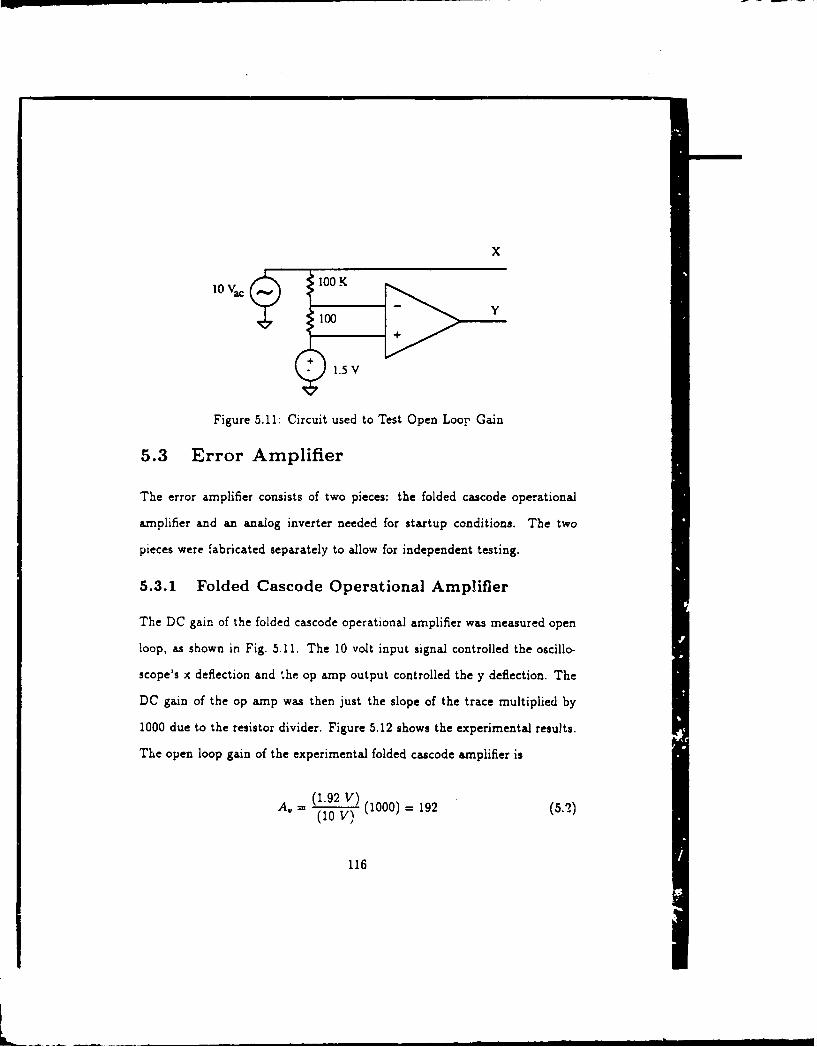
X
100 K10 Vc
Figure 5.11: Circuit used to Test Open Loor Gain
5.3 Error Amplifier
The error amplifier consists of two pieces: the folded cascode operational
amplifier and an analog inverter needed for startup conditions. The two
pieces were fabricated separately to allow for independent testing.
5.3.1 Folded Cascode Operational Amplifier
The DC gain of the folded cascode operational amplifier was measured open
loop, as shown in Fig. 5.11. The 10 volt input signal controlled the oscillo-
scope's x deflection and the op amp output controlled the y deflection. The
DC gain of the op amp was then just the slope of the trace multiplied by
1000 due to the resistor divider. Figure 5.12 shows the experimental results.
The open loop gain of the experimental folded cascode amplifier is
=. (1 92 v)- (10 v) (1000) = 192 (5.q)
116

Figure 5.12: Experimental Results of DC Gain Measurements
117
-L-~ m m m m m m m m mmm m m mm m m l m

The measured gain is a factor of ten smaller than predicted by hand
calculations and simulations. This dramatic decrease in gain is caused by the
failure of the improved cascode current source to properly bias the amplifier.
Figure 5.13 sh,ws +he improved cascode current mirror that was used to bias
the cascoded stage of the operational amplifier. This current mirror was used
to improve the output swing of the amplifier. The improved cascode current
source achieves the increased swing by sizing device M3 at 1/4 the W/L ratio
of transistors M1,M2, and M4. In theory and in simulation, the proposed
biasing scheme provides a VDS of AV across both M5 and M6, as shown
in Fig. 5.13. Thus, for a given drain current, both transistors are right on
the edge of saturation as shown in Fig. 5.14. However, the slightest increase
in the W/4L sizing of device M3 causes the lower device, M6, to enter the
triode region. When the lower device enters the triode region, its output
impedance decreases drastically. As can be seen from in Fig. 5.14, the slope
of the ID vs. VDS curve sharply increases in the triode region, corresponding
to a decreased output impedance.
In the folded cascode circuit shown in Fig. 5.15, the output impedance of
the amplifier was derived assuming a high output impedance of the lower bias
transistors, M3 and M4. Biasing M3 and M4 in the triode region effectively
places a very low impedance in parallel with the high output impedance of
the differential stage. The degraded gain is then
118

V tV+D6
Figure 5.1asn:oio Improved Cascade Current Mirror
D T ri d c S a uratin11 9S

®M17 M1 M22
M2 M8
M6 M" M16 5 IA
Figure 5.15: Folded Cascode Amplifier Circuit
4, = gmIm 4rcO(r*, H R (5.3)
However, the improved cascode current mirror is still a viable bias network
if precaution for non-ideality is taken If transistor M3 of the Fig. 9.13 is sized
to be W,/ L or W/6L, saturation is assured with little sacrifice in output
voltage swing. For instance. a W/6L ratio only reduces output swing to
2.5AV.
The decreased op.n lc.op gain of the amplifier also degrades its common
mode rejection rato and power supply rejection ratio. Common mode rejec-
tion ratio is defined a. ; 1,
CMRR = A (5.4)AC
120
Lm . im

Expected MeasuredCMRR (at DC) 98 dB 75.56 dBPSRR (at DC) 69 dB 46 dB
Table 5.1: Rejection Ratio Degradation Due to Decreased Differential Gain
where AD is the differential gain and AC is the common mode gain. Similarly,
the power supply rejection ratio is defined as [11]
PSRR = AD (55)
Ap
where Ap is the gain at the output to a signal on the power sppty rall.
Since the differential gain, AD, of the experimenta, foided cascode stage
was a factor of ten less than expected, the CMRR and PSRR exhibited a
corresponding factor of ten decrease. The experimental results are shown in
Table 5. 1.
5.3.2 Analog Inverter
As previously discussed, the amplifier output needs to be inverted in order
to feed back a low signal to the primary side when te converter output
was low. The analog inverter was first tested separately before attaching the
operational amplifier. A 1 kHz, 200 mV sine wave was applied to the analog
inverter. The experimental results showing the desired 180 degrees of phase
shift are shown in Fig. 5.16. The top trace is the input signal, the bottom
tiace is the output signal. The maximum output swing of the inverter stage
was 1 Vp-,, siightly lebs than 'he 1.5 volt simulated swing. The cause was a
slightly lower bias voltage from the diode chain used to bias the inverter.
121

Figure 5.16: Input and Output Waveforms of Experimecntal Inverter
122

When connected to the folded cascode operational amplifier, the inverter-
op amp pair exhibited a unity gain bandwidth of 4.93 MHz. This lower than
expected bandwidth resulted from the capacitance added by splitting the
two systems apart. The op amp vas compensated by adding a compensation
capacitor to the output node. Since the amplifier and the inverter were
fabricated separately, connecting them required connecting two external pins
on the IC. The output pin of the operational amplifier and the input pin
of the inverter, with their associated bonding pads, added approximately
20 pF to the compensation capacitor. The added capacitance pushed the
dominant pole lower in frequency and decreased the bandwidth. Connecting
the amplifier and inverter on chip would restore the bandwidth of the system.
In addition, all of the offsets through the inverter were not exactly can-
celed by sizing, as was simulated. The input offset voltage of the amplifier-
inverter pair was 4.64 mV. The offsets produced by the inverter can be at-
tributed to the differences in threshold voltages between the models used for
simulation and the fabricated device:,. Table 5.2 summarizes the test results
of the error amplifier.
5.4 Modulator
A layout mask error prevented experimental testing of the modulator. The
defect occurred over the active area of a transistor such that any FIB repair
would destroy the device. At the the time of this writing, an updated edition
123

Parameter Test Condition unitsInput Offset Voltage V,. = 1.5V 4.64 mVInput Bias Current V, = 1.5V 0 pAInput Offset Current V., = 1.5V 0 uASmall Signal Open Loop Gain 45.66 dBCMRR Va' 1 - 3.5 V 75.56 dBPSRR DC 46 dBOutput Swing 1.0 VMax Sink Current 500 uAMax Source Current 5 mAUnity Gain Bandwidth 4.93 MHz
Table 5.2: Error Amplifier Test Results
of the secondary-side isolated feedb.,ck controller integrated circu~t is being
prepared for submission to MOSIS. The upgraded layout contained subcell
design improvements and connected the individual elements of the circuit.
124

Chapter 6
Conclusion
This thesis described the development of a CMOS secondary side feedback
control integrated circuit. The main functional components of the circuit
were fabricated through the MOSIS program and tested independently.
The bandgap reference circuit provided a voltage reference that was sta-
ble to within ± 0.3% over the commercial 0.70*C temperature range. When
the temperature was increased to include the upper 1250C limit of the mil-
itary temperature range, the circuit was still stable to ± 1.1%. Given the
uncertainty of MOSIS process parameters, the circuits required trimming to
achieve the 0.3% accuracy. The resistor trimming technique was intended
only lor evaluation of the prototype. When the design is targeted for a spe-
cific process, the trimming process could presumably be eliminated.
The oscillator subsection was compiled from a modified library of existing
subcells of power supply control circuitry. The circuits were scaled down
to the two micron process and adapted to function with a 5 volt power
125

supply. All of the subcells demonstrated proper circuit operation, although
each exhibited an explainable performance degradation due to the added
parasitics involved with bringing internal signals off chip for measurement.
The implementation of previously designed CMOS control circuitry in an
upgraded technology demonstrated the versatility of the CMOS technology
for power supply control. Due to the scalable nature of CMOS, existing
libraries of subcells remain viable as technologies improve. Utilizing these
libraries of CMOS subcells facilitates rapid implementation of application-
specific control circuitry.
The error amplifier demonstrated a disappointing factor of ten decrease
in gain from that predicted by simulation. The cause was traced to a de.
sign error in the improved cascode current source used to bias the amplifier.
Resizing one device would eliminate the biasing problem and restore perfor-
mance.
The implementation of the feedback controller IC also involved an inves-
tigation into the use of a Focused Ion Beam for integrated circuit repair.
Experiments with samples of the feedback controller IC demonstrated the
feasibility of both connecting and severing aluminum lines with the Focused
Ion Beam. Unfortunately, the modulator subcell layout contained an error
that was unrepairable with the FIB, rendering the circuit inoperable.
Opportunities for future work include combining all of the subcells pre-
sented in this thesis into a monolithic integrated circuit and testing the con-
126

troller in a prototype power converter. An additional application of CMOS
control circuitry includes integrating the primary -idz contro!. In current
point-of-load converters, the demodulation of the amplitude modulated feed-
back signal is accomplished with a peak detection circuit implemented with
discrete components. Integration of the demodulator circuit with the primary
side control circuitry would allow further reduction of converter size.
127

Appendix A
Microphotographs ofIntegrated Circuits
Figure A.1 is a microphotograph oi the integrated circuit fabricated to test
the functional blocks of the feedback controller. Starting from the lower left-
hand corner and proceeding counter-clockwise, the circuit blocks are: the
Schmitt-trigger oscillator, the divider, the phase splitter, the error amplifier,
the modulator, the error amplifier inverter, the bandgap operational ampli-
fier, and two complete bandgap reference circuits.
Figure A.2 is a microphotograph of the integrated circuit fabricated to
test the bandgap reference circuit. The chip contains six bandgap zircuits,
three along the left side, three along the right side, Ns well a. individual
resistors and bipolar transistors.
128
L ,=__•=-=lm.,m.,,I•Ii i i = i

Figure A+l. Fabrication of Separate Functional Blocks
129

Figure A.2: Fabrication of Baridgap Circuits
130

Bibliography
[1] J.G. Kassakian, and M.F. Schlecnt, "High-Frequency High-Density Con-verters for Distributed P- -r Supply System.," Proceedings of the IEEE,Vol. 76, No. 4, April . pp. 362-376.
[2] initrode Linear I( Zdtabook, Unitrode Corporation, Lexington, Mas-sachusetts, 198" 1988.
[3] Yannis P. -, sividis and Richard W. Ulmer, "A CMOS Voltage Refer-ence," IFLE J. Solid-State Circuits, Vol SC-13, No. 6, Dec. 1978, pp.774- 77F
[4] P.R. Gray and R.G. Meyer, "MOS Operational Amplifier Design - AT.torial Overview," IEEE J. Solid-State Circuits, Vol. SC-17, Dec. 1982,No. 6, pp. 969-982.
[5] P.R. Gray and R.G. Meyer, Analysis and Design of Anilog IntegratedCircuits (John Wiley and Sons, New York, 1984).
[6] J. Michejda and S.K. Kim, "A Precision CMOS Bandgap Reference,"IEEE J. Solid-State Circuits, Vol SC-19, No. 6, Dec. 1984, pp. 1014-1021.
[7] K.M. Ware, A High-Frequency Integrated CMOS Phase-Locked Loop,Doctoral Thesis, Department of Electrical Engineering and ComputerScience, M.I.T., 1989.
[8] N.Weste and K. Eshraghian. Principles of CMOS VLSI Design(Addison-Wesley Publishing Co., Reading, Massachusetts, 1985).
[9] A.B. Grebene, Bipolar and MOS Analog Integrated Circuit Design (JohnWiley and Sons, New York, 1984)
[10] L.F. Casey, Circuit Design for 1-10 MHz DC-DC Conversion, DoctoralThesis, Department of Electrical Engineering and Computer Science,M.I.T., 1989.
131

[111 R. Gregorian and G. C. Temes, Analog MOS Integrated Circuits forSignal Processing (John Wiley and Sons, New York, 1986).
[121 J. Meingailis and C.R. Musil, "The focused ion beam as an integratedcircuit restructuring tool," J. of Vacuum Science and Technology, Vol4, No. 1, Jan-Feb. 1986, pp. 176-180.
[131 M.F. Schlecht and L.F. Casey, "Comparison of the Square-Wave andQuasi-Resonant Topologies," IEEE PESC Record, 1987, pp. 124-134.
132