IIIIIlIMlUll[lIMlllllllll IIIlllIlllllllllllU - NASA · A.H. Gomes de Mesquita in Acta...
56
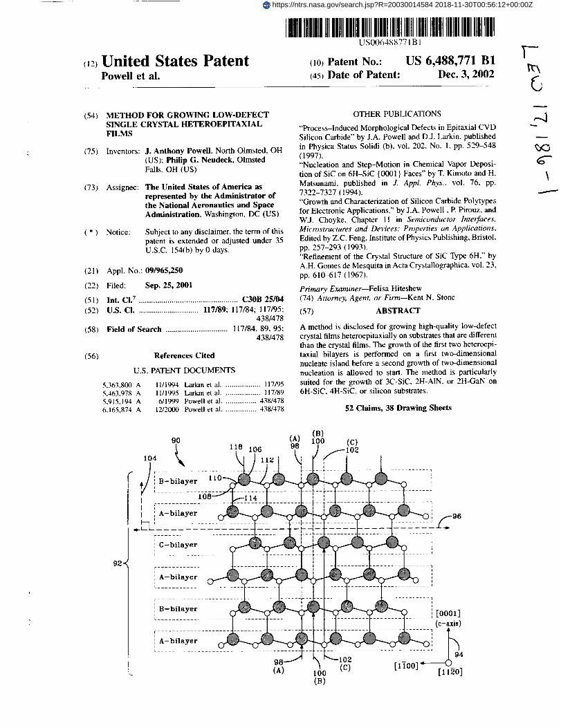
(12)United States Patent Powell et al. IIIIIlIMlUll[lIMlllllllll IIIlll IlllllllllllU III III US00648877 1B 1 (10) Patent No.: US 6,488,771 B1 (45) Date of Patent: Dec. 3, 2002 T- C (54) METHOD FOR GROWING LOW-DEFECT SINGLE CRYSTAL HETEROEPITAXIAL FILMS (75) Inventors: (73) Assignee: (*) Notice: J. Anthony Powell. North Olmsted, OH (US); Philip G. Neudeck, Olmsted Falls, OH (US) The United States of America as represented by the Administrator of the National Aeronautics and Space Administration, Washington, DC (US) Subject to any disclaimer, the term of this patent is extended or adjusted under 35 U.S.C. 154(b) by 0 days. (21) Appl. No.: 091965,250 (22) Filed: Sep. 25, 2001 (5 I) Int. CI. 7 ................................................ C30B 25104 (52) U.S. CI .............................. 117/89; 117/84; 117/95; 438/478 (58) Field of Search .............................. 117/84, 89, 95: 4381478 (56) References Cited U.S. PATENT DOCUMENTS 5,363,800 A 11/1994 Larkin et al .................. 117/95 5,463,978 A 11/1995 Larkin et al .................. 117/89 5,915,194 A 6/1999 Powell et al ................ 438/478 6,165,874 A 1_2000 Powell et al ................ 438/478 92"< 90 104 L r _ B-bilayer I I ; I ', A-bilayer I C-bilayer A-bilayer B-bilayer I A-bilayer 118 106 110_ (A) OTHER PUBLICATIONS "Process-lnduced Morphological Defects in Epitaxial CVD Silicon Carbide" by J.A. Powell and D.J. Larkin, published in Physica Status Solidi (b), vol. 202, No. 1, pp. 529-548 (1997). "Nucleation and Step-Motion in Chemical Vapor Deposi- tion of SiC on 6H-SiC {0001 } Faces" by T. Kimoto and H. Matsunami, published in J. Appl. Phys., vol. 76, pp. 7322-7327 (1994). "Growth and Characterization of Silicon Carbide Polytypes for Electronic Applications." by J.A. Powell, P. Pirouz, and W.J. Choyke, Chapter 11 in Semiconductor Interfaces, Microstructures and Devices: Properties an Applications, Edited by Z.C. Feng, Institute of Physics Publishing, Bristol, pp. 257-293 (1993). "Refinement of the Crystal Structure of SiC Type 6H," by A.H. Gomes de Mesquita in Acta Crystallographica, vol. 23, pp. 610-617 (1967). Primary Examiner--Felisa Hiteshew (74) Attorney. Agent, or Firnz--Kent N. Stone (57) ABSTRACT A method is disclosed for growing high-quality low-defect crystal films heteroepitaxially on substrates that are different than the crystal films. The growth of the first two heteroepi- taxial bilayers is performed on a first two-dimensional nucleate island before a second growth of two-dimensional nucleation is allowed to start. The method is particularly suited for the growth of 3C-SiC, 2H-AIN, or 2H-GaN on 6H-SiC, 4H-SiC, or silicon substrates. 52 Claims, 38 Drawing Sheets (B) (A) I00 (C) 98 (c) 100 (_) %<3 I https://ntrs.nasa.gov/search.jsp?R=20030014584 2018-11-30T00:56:12+00:00Z
Transcript of IIIIIlIMlUll[lIMlllllllll IIIlllIlllllllllllU - NASA · A.H. Gomes de Mesquita in Acta...
(12)United States PatentPowell et al.
IIIIIlIMlUll[lIMlllllllllIIIlllIlllllllllllUIIIIIIUS00648877 1B 1
(10) Patent No.: US 6,488,771 B1
(45) Date of Patent: Dec. 3, 2002
T-
C
(54) METHOD FOR GROWING LOW-DEFECTSINGLE CRYSTAL HETEROEPITAXIALFILMS
(75) Inventors:
(73) Assignee:
(*) Notice:
J. Anthony Powell. North Olmsted, OH
(US); Philip G. Neudeck, Olmsted
Falls, OH (US)
The United States of America as
represented by the Administrator ofthe National Aeronautics and SpaceAdministration, Washington, DC (US)
Subject to any disclaimer, the term of thispatent is extended or adjusted under 35
U.S.C. 154(b) by 0 days.
(21) Appl. No.: 091965,250
(22) Filed: Sep. 25, 2001
(5 I) Int. CI. 7 ................................................ C30B 25104
(52) U.S. CI .............................. 117/89; 117/84; 117/95;438/478
(58) Field of Search .............................. 117/84, 89, 95:4381478
(56) References Cited
U.S. PATENT DOCUMENTS
5,363,800 A 11/1994 Larkin et al .................. 117/955,463,978 A 11/1995 Larkin et al .................. 117/895,915,194 A 6/1999 Powell et al ................ 438/4786,165,874 A 1_2000 Powell et al ................ 438/478
92"<
90
104 L
r _ B-bilayer
II ;I ', A-bilayer
I C-bilayer
A-bilayer
B-bilayer
I A-bilayer
118 106
110_
(A)
OTHER PUBLICATIONS
"Process-lnduced Morphological Defects in Epitaxial CVD
Silicon Carbide" by J.A. Powell and D.J. Larkin, published
in Physica Status Solidi (b), vol. 202, No. 1, pp. 529-548
(1997).
"Nucleation and Step-Motion in Chemical Vapor Deposi-
tion of SiC on 6H-SiC {0001 } Faces" by T. Kimoto and H.
Matsunami, published in J. Appl. Phys., vol. 76, pp.7322-7327 (1994).
"Growth and Characterization of Silicon Carbide Polytypes
for Electronic Applications." by J.A. Powell, P. Pirouz, and
W.J. Choyke, Chapter 11 in Semiconductor Interfaces,
Microstructures and Devices: Properties an Applications,
Edited by Z.C. Feng, Institute of Physics Publishing, Bristol,
pp. 257-293 (1993)."Refinement of the Crystal Structure of SiC Type 6H," by
A.H. Gomes de Mesquita in Acta Crystallographica, vol. 23,
pp. 610-617 (1967).
Primary Examiner--Felisa Hiteshew(74) Attorney. Agent, or Firnz--Kent N. Stone
(57) ABSTRACT
A method is disclosed for growing high-quality low-defect
crystal films heteroepitaxially on substrates that are differentthan the crystal films. The growth of the first two heteroepi-
taxial bilayers is performed on a first two-dimensionalnucleate island before a second growth of two-dimensional
nucleation is allowed to start. The method is particularly
suited for the growth of 3C-SiC, 2H-AIN, or 2H-GaN on6H-SiC, 4H-SiC, or silicon substrates.
52 Claims, 38 Drawing Sheets
(B)(A) I00 (C)98
(c)100
(_)
%<3
I
https://ntrs.nasa.gov/search.jsp?R=20030014584 2018-11-30T00:56:12+00:00Z

U.S. Patent Dec. 3, 2002 Sheet 1 of 38 US 6,488,771 B1
34
39
CP
REG
31a
35
38-,
FIG-IN2
(CP_
(REG
34
CP_ CP _
35 35 35
H2

U.S. Patent Dec. 3, 2002 Sheet 2 of 38 US 6,488,771 B1
FIG-2/
C-AXIS <0001>
Si
ISi Si Si
l l
24
Si /,---50Si
I
C C C C C
FIG-352
// " !
FIG
24
U.S. Patent Dec. 3, 2002 Sheet 3 of 38 US 6,488,771 B1
7O72 72
72A B 72
A C
24D
A
72
66
JB
FIG-5A
68B-_
/A
72 72 72 72
B A C A
72
/B
,_68A
FIG-5B

U.S. Patent Dec. 3, 2002 Sheet 4 of 38 US 6,488,771 B1
24D
72 ____-74 l/ 72
A j / 7266__ / B / j 72 72
)
68B_ _ ___.--_68A
FIG-6A
66
\B
68B _
_--68A
FIG-6B

U.S. Patent Dec. 3, 2002 Sheet 5 of 38 US 6,488,771 B1
24D
°C J oo"B_ I 78A 80
kB_ 84
68B _ _68A
FIG-7A
68B _
66 B
78A
_80
8O
_68A
FIG-7B

U.S. Patent Dec. 3, 2002 Sheet 6 of 38 US 6,488,771 B1
66 24D
/B 80 J
_- , 82
68B_. ' _ 7_6;8 A
FIG-SA
68B _
B 66
80 A
FIG-SB

U.S. Patent Dec. 3, 2002 Sheet 7 of 38 US 6,488,771 B1
66 24D
76 1 82
68B-_ _68A
FIC-9A
68A
68B A
FIG-9B

U.S. Patent Dec. 3, 2002 Sheet 8 of 38 US 6,488,771 B1
78B
6,680 C | 24D
rn Ill \ 80B 80A 78A
FIG-IOAPRIOR ART
B
8 A
o,,-.-I o p////////////////_
FIG-10BPRIOR ART

U.S. Patent Dec. 3, 2002 Sheet 9 of 38 US 6,488,771 B1
78B
6,6 | 84 Z4D
'/_ - 82
88B_''" _SA-
FIG-1 1APRIOR ART
84
FIG-1 1BPRIOR ART

U.S. Patent Dec. 3, 2002 Sheet 10 of 38 US 6,488,771 B1
78B
68B _
84A
78A68A
84
FIG-12PRIOR ART

U.S. Patent Dec. 3, 2002 Sheet 11 of 38 US 6,488,771 B1
FIG --13A
Z
-- 78E
_66
WIDTH W
-<
f
_If66
88
66
IL_2 -_
LA=LI+L2
FIG 13B

U.S. Patent Dec. 3, 2002 Sheet 12 of 38 US 6,488,771 B1
I
I I
I II I
I I
I I
I I
I
i I
I I
I I I
I I I
I
I
I
I
I

U.S. Patent Dec. 3, 2002 Sheet 13 of 38 US 6,488,771 B1
I I I
II
I I
Y
I
I

U.S. Patent Dec. 3, 2002 Sheet 14 of 38 US 6,488,771 B1
108
i08_
w,..
108_
'_ 132
/ \108 , , ,/ l \
| , , . _....x_---, I06
\\\
1
i08_'-"
08
FIG-15B
10610_06
.---106
FIG- 15C lo8_ ,' _._,
106_ _106J

U.S. Patent Dec. 3, 2002 Sheet 15 of 38 US 6,488,771 B1
f
©II
II
I
o ®II
II
I
o ®I
I!
II
o ®I
I!
I
o ®II
II
o ®
©
Ir_

U.S. Patent Dec. 3, 2002 Sheet 16 of 38 US 6,488,771 B1
• I_
O0
_--_ _= r -_ _
>-
<
I
Y
U.S. Patent Dec. 3, 2002 Sheet 17 of 38 US 6,488,771 B1
_--_.______.__---_
p,,.
I
U.S. Patent Dec. 3, 2002 Sheet 18 of 38 US 6,488,771 B1
CD
I

U.S. PatentDec. 3, 2002
Sheet 19 of 38US 6,488,771 BI

U.S. Patent Dec. 3, 2002 Sheet 20 of 38 US 6,488,771 B1
I
I

U.S. Patent Dec. 3, 2002 Sheet 21 of 38 US 6,488,771 B1
¢Q
I l
I
I
l
<
)

U.S. Patent Dec. 3, 2002 Sheet 22 of 38 US 6,488,771 B1
._ . _/'-_Oi I • _ I •
I I •I l
I I _
I I /I
- I I _ I v
I
I I
II I
I
0
I

U.S. Patent Dec. 3, 2002 Sheet 23 of 38 US 6,488,771 B1
II
II
;
I II II I
I II I

U.S. Patent Dec. 3, 2002 Sheet 24 of 38 US 6,488,771 B1
Y

U.S. Patent Dec. 3, 2002 Sheet 25 of 38 US 6,488,771 B1
J

U.S. Patent Dec. 3, 2002 Sheet 26 of 38 US 6,488,771 B1
Ir_o
J

U.S. Patent Dec. 3, 2002 Sheet 27 of 38 US 6,488,771 B1
• I I
II
I
<
#

U.S. Patent Dec. 3, 2002 Sheet 28 of 38 US 6,488,771 B1
II
II
I
I I
II
<_
J
k('3C_
I

U.S. Patent Dec. 3, 2002 Sheet 29 of 38 US 6,488,771 B1
I!
C
!I
!
II
I
Ik.I
<
,2
I

U.S. Patent Dec. 3, 2002 Sheet 30 of 38 US 6,488,771 B1
24D
. L B ao vaBi_.-_\ J l I vaA
76_ •
68B--_ __8A
FIG-27A
68B _
B
A
78B
FIG-27B

U.S. Patent Dec. 3, 2002 Sheet 31 of 38 US 6,488,771 B1
24D
82 78C l
t ] 78B
FIG-28A
68B
78C
FIG-28B
_-78A
_68A
78B

U.S. Patent Dec. 3, 2002 Sheet 32 of 38 US 6,488,771 B1
150 DPB_ i5o
B2__ _ l 150
A B
76 82
68B_ _"-68A
FIG-29A
82-_
DPB 150
FIG-29B
82

U.S. Patent Dec. 3, 2002 Sheet 33 of 38 US 6,488,771 B1
\
I I
I I
I I
I I
I I
I
I
U.S. Patent Dec. 3, 2002 Sheet 34 of 38 US 6,488,771 B1
..... J
\
I
I Ib I
I I
IIIIII
<..... _J
Ycz3
_=_
<
J
I

U.S. Patent Dec. 3, 2002 Sheet 35 of 38 US 6,488,771 B1
@ ®
@
®
@
@
@
@
tt_
I

U.S. Patent Dec. 3, 2002 Sheet 36 of 38 US 6,488,771 B1
F _---4 I,p-4
1 i I....J
r"-'l
II
r@]I II I
IIII
IL?
I
\Y
J
U.S. Patent Dec. 3, 2002 Sheet 37 of 38 US 6,488,771 B1
OFI
•lII
II

U.S. Patent Dec. 3, 2002 Sheet 38 of 38 US 6,488,771 BI
cDT-4

US 6,488,771 B 1
1
METHOD FOR GROWING LOW-DEFECTSINGLE CRYSTAL HETEROEPITAXIAL
FILMS
ORIGIN OF THE INVENTION
The invention described herein was made by employees
of the United States Government and may be used by or for
the Government for governmental purposes without pay-
ment of any royalties thereon or therefor.
FIELD OF THE INVENTION
The invention relates to the growth of semiconductor
device crystal films, and more particularly, to a method for
producing high quality films of silicon carbide (SIC), alu-
minum nitride (A1N), gallium nitride (GaN), and other
materials or compounds on atomically fiat crystalline sur-
faces. Specifically, the invention enables the growth of low
defect heteroepitaxial single crystal films on atomically flat
crystal surfaces. The semiconductor devices find application
in high power, high frequency, high temperature and high
radiation environments, as well as use in optoelectronicdevices such as lasers and light-emitting diodes.
BACKGROUND OF THE INVENTION
This invention relates to the controlled growth of crystal
films for application to the fabrication of semiconductor
devices. The invention is particularly applicable to the
production of crystals (herein used to include crystal films)of silicon carbide, aluminum nitride, gallium nitride,
diamond, and other materials. A primary aspect of theinvention is related to silicon carbide (SIC) and the nitrides
(e.g., A1N and GaN) of the Group III elements; however, theinvention has much broader applications and can be used for
other elemental crystals and compounds. For example, films
of ternary and quaternary compounds (and higher order
compounds) of the III-V elements (e.g., GaAIN) could be
grown. Also. elemental single crystal films, such as silicon
and diamond could also be grown.
The term "'atomically-flat" is known in the art and is
generally referred to herein as meaning a surface that is
totally without any atomic-scale or macro-scale steps overan area defined by selected boundaries that may be created
by grooves in a manner to be further described herein with
reference to FIG. 4. Many of the methodologies of thepresent invention are shared with that of U.S. Pat. No.
5,915,194, as well as U.S. Pat. No. 6,165,874, both of which
are herein incorporated by reference.
Semiconductor devices, including MISFETs and otherdevice structures all related to the present invention, are used
in a wide variety of electronic applications. Semiconductor
devices include diodes, transistors, integrated circuits,
sensors, and opto-electronic devices, such as light-emittingdiodes and diode lasers. Various semiconductor devices
using silicon or compound semiconductors, such as gallium
arsenide (GaAs) and gallium phosphide (GAP) are com-
monly used. In order to fabricate semiconductor devices, it
is necessary to be able to grow high-quality, low-defect-
density single-crystal films with controlled impurity incor-poration while possessing good surface morphology. The
substrate upon which the film is grown should also be a
high-quality, low-defect-density single crystal. In recent
years, there has been an increasing interest in research on
wide-bandgap semiconductors for use in high temperature,
high power, high frequency, and/or high radiation operating
2conditions under which silicon and conventional III-V semi-
conductors cannot adequately function. Particular researchemphasis has been placed on SiC, and llI-nitride alloys,including A1N, GaN, lnGaN, AIGaN, and others.
5 Conventional semiconductors are unable to meet some of
the increasing demands of the automobile and aerospaceindustries as they move to smarter and more electronic
systems. New wide bandgap materials are being developedto meet the diverse demands for more power at higher
l0 operating temperatures. Two of the most promising emerg-ing wide bandgap semiconductors are silicon carbide (SiCI
and gallium nitride (GaN). At over three electron volts, the
bandgap of these materials is nearly three times as large as
that of silicon. This advantage theoretically translates into
15 very large improvements in power handling capabilities and
higher operating temperatures that will enable revolutionary
product improvements. Once material-related technology
obstacles are overcome, SiC's properties are expected to
dominate high power switching and harsh-environment
20 electronics for manufacturing and engine control
applications, while GaN will enable high power high fre-
quency microwave systems at frequencies beyond 10 GHz.
To date the best SiC devices to our knowledge are homo-
junction (i.e., wafer and device layers are all hexagonal25 SIC), while GaN devices are heterojunction (i.e., SiC or
sapphire wafers with device layers of GaN, AIGaN, A1N,
etc.) because production of bulk GaN wafers is not practicalat the present time.
Silicon carbide crystals exist in hexagonal, rhombohedral
30 and cubic crystal structures. Generally, the cubic structure,
in particular, the zincblende structure is referred to as 13-SICor 3C-SiC, whereas numerous polytypes of the hexagonal
and rhombohedral structures are collectively referred to as
a-SiC. To our knowledge, only bulk (i.e., large) crystals of
35 the a polytypes have been grown to date with reasonable
quality and size acceptable for device applications. The 13(or3C) potytype can only be obtained as small (less than 1 cm 2)
blocky crystals or thick epitaxial films on small 3C sub-
strates or crystal films of poor quality grown heteropitaxially
40 on some other substrate. The most commonly availablea-SiC polytypes are 4H-SiC and 6H-SiC; these are com-
mercially available as polished wafers, presently up to 75
mm in diameter. Each of the SiC polytypes has its own
specific advantages over the others. For example, (lj
45 4H-SiC has a significantly higher electron mobility com-pared to 6H-SiC; (2) 6H-SiC is used as a substrate for the
commercial fabrication of GaN blue light-emitting diodes
(LED's); and (3) 3C-SiC has a high electron mobility similar
to that of 4H-SiC and may function over wider temperature
50 ranges, compared to the ct polytypes, but crystals of suffi-
cient quality and size have not been readily obtainable.
Silicon carbide polytypes are formed by the stacking of
double layers, also referred to as bilayers, of covalentlybonded Si and C atoms. As will be more fully described
55 later, each double layer may be situated in one of three
atomic stacking positions known as A, B, and C. The
sequence of stacking determines the particular polytype; forexample, the repeat sequence for 3C-SiC is ABCABC... (orACBACB . . . ) the repeat sequence for 4H-SiC is ABA-
60 CABAC... and the repeat sequence for 6H is ABCACBAB-
CACB... From this it can be seen that the number in the
polytype designation gives the number of double layers in
the repeat sequence and the letter denotes the structure type
(cubic, hexagonal, or rhombohedral). The stacking direction65 is designated as the crystal c-axis and is in the crystal
<0001> direction: it is perpendicular to the basal plane
which is the crystal 10001) plane. The SiC polytypes are

US 6,488,771
3
polar in the <0001> directions; in one direction, the crystalface is terminated with silicon (Si) atoms; in the other
direction, the crystal face is terminated with carbon (C)atoms. These two faces of the (0001) plane are known as the
silicon face (Si-face) and carbon face (C-face), respectively. 5
As will be more fully described later with respect to FIG.
15(A), the 3C-SiC (i.e., cubic) polytype has four equivalent
stacking directions, and thus there are four equivalent
planes, the (111) planes, that are basal planes. As used
herein, "basal plane" shall refer to either the (0001) plane for It
a or-SiC, or the (111) plane of 3C-SiC. The term "vicinal(0001) wafer" shall be used herein for wafers whose pol-
ished surface (the growth surface) is misoriented less than
10 ° from the basal plane. The angle of misorientation shallbe referred to herein as the tilt angle. The term "homoepi- t5
taxial" shall be referred to herein as epitaxial growth,
whereby the film and the substrate (wafer) are of the same
polytype and material, and the term "heteroepitaxial" shall
be referred to herein as epitaxial growth whereby the film is
of a different polytype or material than the substrate. The 20term "mesa" is meant to represent an isolated growth region
to be further described herein. The term "bilayer" shall be
referred to herein as a layer along the basal plane consisting
of two-tightly bonded monolayers of atoms, such as Si and
C atoms tightly bonded in bilayers of SiC to be further 25described. The term "defect free" shall be referred to herein
as a single crystal that is free of extended structural defects,
such as dislocations and stacking faults that propagate overnumerous atoms in at least one direction. The term "defect
free" is not meant to describe isolated point defects that 30
involve at most 1 or 2 atoms at an isolated 3D point in the
crystal, such as atomic vacancy point defects, interstitial
point defects, and impurity point defects.
Theories explaining epitaxial single-crystal growth are
well known. Crystal growth can take place by several 35
mechanisms. Two of these are: ( 1) growth can take place by
the lateral growth of existing atomic-scale steps on the
surface of a substrate and (2) growth can take place by theformation of two-dimensional atomic-scale nuclei on the
surface followed by lateral growth from the steps formed by 40
the nuclei. The lateral growth from steps is sometimes
referred to as "step-flow growth." In the first mechanism,
growth proceeds by step-flow from existing steps without
the formation of any two-dimensional nuclei (i.e., without2D nucleation). In the nucleation mechanism, the nucleus 45
must reach a critical size in order to be stable: in other
words, a potential energy barrier must be overcome in orderfor a stable nucleus to be formed. Contamination or defects
on the substrate surface can lower the required potential
energy barrier at a nucleation site. In the processes described 50
in U.S. Pat. No. 5,915,194, having certain drawbacks related
to lattice mismatch giving rise to undesired crystal defects,
crystal growth proceeds by (1) step flow without 2D nucle-ation or by (2) step-flow with 2D nucleation. Step-flow
growth with 2D nucleation allows the growth of epitaxial 55films of any desired thickness. In the processes described in
the present invention, optimum growth (i.e., defect free)
occurs when a first bilayer and a second bilayer are com-
pleted from lateral step-flow expansion of single nucleationislands of heteroepitaxial film on an atomically fiat surface. 60
As discussed above, as well as in U.S. Pat. No. 5,915,194,
3C-SiC, to our knowledge, is not available in high quality
single-crystal large wafer form. Hence, 3C-SiC device struc-
tures must be grown heteroepitaxially on some other sub-
strate material. The present invention overcomes the prob- 65
lems of prior art, including recently discovered deficienciesof U.S. Pat. No. 5,915,194 to be further described, to realize
B1
4
the growth of high quality low-defect 3C-SiC films on6H-SiC and 4H-SiC substrates.
In addition to non-availability of high quality 3C-SiCsingle crystal wafers or epilayers, other wide-bandgap semi-conductor compounds that are not available in single-crystalwafer form and which have great commercial potential are
the nitrides of aluminum, gallium, and indium. Galliumnitride (GaN) in particular, has great potential as an opto-
electronic material. Currently, commercial light-emittingdiodes are being fabricated by growing GaN or lnGaN films
on 6H-SiC or sapphire substrates. Even though these filmshave extremely high defect densities (typically around l0 s
cm-Z), very bright and efficient LED's can be fabricated.Pulsed blue lasers have been fabricated from lii-N, as well
as continuous blue lasers that operate for a period of time
before failure related to crystal defects. The present inven-
tion provides a means for reducing defects in the GaN andInGaN films and hence makes a more durable continuous
duty III-N laser possible.
Although U.S. Pat. No. 5,915,194, as well as U.S. Pat. No.6,165,874, provides many benefits, it has certain limitations.
In our practice of the teachings of U.S. Pat. No. 5,915,194,it has been determined that other defects, not related to
surface steps, form when practicing heteroepitaxial growthon atomically flat surfaces as taught by U.S. Pat. No.
5,915,194. As pointed out in U.S. Pat. No. 5,915,194,heteroepitaxial growth on an atomically flat basal plane
starts by the nucleation of a growth island that consists of a
bilayer of tightly bonded Si and C atoms. In U.S. Pat. No.5,915,194, as illustrated in FIGS. 7 and 8 thereof, it is
described that multiple growth islands (Reference #46 in
FIG. 7 thereof) nucleated on the flat surfaces would coalesce
without defects because the atoms of the expanding islands
would remain coherent with the substrate crystal lattice.
However, recent experimental observations in growing het-
eroepitaxial 3C-SiC films on atomically flat 6H and 4H-SiCsubstrates indicate this is not the case. In reality, numerous
stacking faults are experimentally observed when nucleationof multiple islands takes place within a given atomically flat
mesa surface.
The present invention prevents the occurrence of these
stacking faults while enabling the growth of low-defectheteroepitaxial single crystal films on atomically fiat single
crystal surfaces. The present invention overcomes deficien-cies in prior art, including those of U.S. Pat. Nos. 5,915,194and 5,363,800 (herein incorporated by reference), as well as
those of U.S. Pat. No. 6,165,874, while initiating growth of
heteroepitaxial single crystal films on device-size regions of
atomically fiat substrate surfaces.
OBJECTS OF THE INVENTION
It is a primary object of the present invention to provide
a method of growing high quality low-defect crystal films ofsemiconductors on substrates that are different than the
crystal film. The method is particularly suited for the growthof 3C-SiC, 2H-AIN, and 2H-GaN or InGaN on 6H/4H-SiC
substrates.
It is another object of the present invention to provide a
method of growing III-N heteroepitaxial films on atomicallyfiat surfaces of 6H/4H-SiC substrates.
It is still a further object of the present invention to
provide high quality heteroepitaxial growth of materialswith relatively large lattice mismatch to the substrate, yield-
ing heterojunctions.
It is still another object of the present invention toeliminate the need for buffer layers that are required by prior
art to overcome lattice mismatch in single-crystal heteroepi-taxial films.

US 6,488,771B15
Moreover, it is an object of the present invention to
provide a method that produces devices that are comprised
of reduced defect material having an extended operational
life, reduced power consumption, and reduced size thereby
decreasing production costs.
SUMMARY OF THE INVENTION
The practice of the present invention particularly related
to atomically-fiat crystalline surfaces and crystal films is
partially based on our discovery of that by selecting a
particular set of growth conditions intended to greatlyreduce the rate of two-dimensional (2D) nucleation, we
reproducibly achieve the growth of 3C-SiC heterofilms
entirely free of stacking faults. We also discovered that after
initial 3C-SiC nucleation was carried out on a step-free
surface at a low nucleation rate, that we could then change
the growth conditions to greatly increase the nucleation rate
without any detriment to the quality of the heteroepitaxial
film. These discoveries strongly indicate that optimum
growth (i.e., defect-free) occurs when a first bilayer and a
subsequent second layer is completed from the lateral step-
flow expansion of single nucleation islands (one island for
each bilayer) of the heteroepitaxial film on the atomically-flat surface.
In general, the invention is a method of producing low-
defect crystal film structures of materials that are not pres-
ently available in the form of large area single-crystal
substrates. This method is accomplished by utilizing par-
ticular heteroepitaxial growth processes on an atomically-
flat basal plane surface of a substrate of different material
and/or structure other than the desired crystal film.
The method is primarily concerned with depositing a
heteroepitaxial single-crystal film on a plurality of step-free
surfaces of a basal plane surface orientation of a selected
single-crystal substrate material serving as a wafer. The
method comprises the steps of:
(a) preparing more than one step-free planar surface on
the selected substrate, wherein each of the plurality ofstep-free surfaces has a boundary of selected size and
shape;
(b) selecting a heteroepitaxial film material whose chemi-cal bonding structure is tetrahedral and exhibits a
property that under predetermined growth conditions
that growth of the heteroepitaxial film material grows
in bilayers on the selected step-free planar surface;
(c) carrying out a selected deposition process under
selected growth conditions that produce (1) a single
nucleus of the heteroepitaxial film material at least one
bilayer thick on the step-free surface with the selected
boundary, followed by (2) lateral expansion of the
single nucleus over an entire surface defined by the
selected boundary of the plurality of step-free basal
plane surfaces before a second nucleus can form else-
where on the selected step-free planar surface, and (3)
a single nucleus of the second bilayer of heteroepitaxial
film, followed by (4) lateral expansion of the single
nucleus over the entire surface defined by the selected
boundary before a second nucleus can form elsewhere
on the first bilayer of heteroepitaxial film on the
selected step-free planar surface, and
(d) providing growth of subsequent additional bilayers of
the said heteroepitaxial film by providing a suitable setof growth conditions until a desired thickness of said
heteroepitaxial film is achieved.
Further, the present invention relates to a method of
growing high-quality low-defect single crystal films of sili-
6
con and diamond materials on substrates that are different
than the film. As an example, the growth of 3C-SiC,2H-A1N, and/or 2H-GaN on 6H-SiC substrates is related tothe present invention.
5 A specific application of this invention is the growth of3C-SiC on a 6H-SiC substrate. Another application is thegrowth of 2H-GaN on a 6H-SiC substrate. Other SiCpolytypes, such as 4H-SiC could also be used as substrates
in the practice of this invention.
10 In the practice of our invention, important considerationsto achieve growth with little or no two-dimensional nucle-
ation are the following: contamination and surface defectsmust be minimized because the contamination's can reduce
the energy barrier that hinders two-dimensional nucleation.
Also line defects (dislocations) that intersect the growth15 surface must be minimized because some dislocations act as
localized step sources that can dominate growth on the
substrate mesas preventing the achievement of atomically-
flat or nearly atomically-fiat mesas necessary for the practiceof the present invention.
20 A further consideration related to the invention is that
multiple rotational orientations of the polytypic stacking
sequence can occur on surfaces with steps when a 3C
sequence is grown on a higher order polytypic substrate,
such as a 4H or a 6H polytypic sequence. When crystal film25 islands, that have different rotational orientations, coalesce,
then defects such as double positioning boundaries (DPB's)
form at a boundary between the two domains. It is expected
that this same behavior holds for the 2H sequence grown on
the 4H or 6H sequence.30
BRIEF DESCRIPTION OF THE DRAWINGS
FIG. 1 is a schematic drawing of a CVD system employed
for the growing crystal films in accordance with the presentinvention.
35 FIG. 2 illustrates a plan view of a hexagonal crystal
showing the crystallographic directions of the crystal.FIG. 3 is a cross-sectional view of an or-SiC substrate
showing the Si-face, the C-face and the A-face of thesubstrate.
40 FIG. 4 is a plan view of a substrate that has been divided
into isolated growth regions (mesas) by etching trenches or
grooves.
FIG. 5 is composed of FIGS. 5(A) and 5(B) that cumu-
latively illustrate a polished 4H-SiC wafer mesa having45 undesired steps in its top surface.
FIG. 6 is composed of FIGS. 6(A) and 6(B) that cumu-
latively illustrate a SiC wafer mesa having an atomically-flat
surface created by a step-flow deposition of a homoepitaxialfilm.
50FIG. 7 is comprised of FIGS. 7(A) and 7(B) showing the
initial nucleation and growth of a 3C-SiC bilayer island on
an SiC mesa in accordance with the practice of the presentinvention.
55 FIGS. 8A and 8B illustrates the further growth of the3C-SiC bilayer island of FIG. 7.
FIG. 9 is composed of FIGS. 9(A) and 9(B) that illustrate
the completion of the first 3C-SiC island that is accom-
plished without the allowance of any stacking faults and,
60 thus, is essentially defect free.
FIG. 10 is composed of FIGS. 10(A) and IO(B) that
begins to illustrate the problems associated with the prior art
method, wherein nucleation of multiple bilayer islands ispermitted, not suffered by the present invention.
65 FIG. 11 is composed of FIGS. II(A) and II(B) that
illustrate the formation of a point of incoherent coalescence
that forms a stacking error in the prior art process.

US 6,488,771
7
FIG. 12 illustrates a stacking fault that is an extendedcrystal defect caused by prior art processes.
FIG. 13 is composed of FIGS. 13(A) and 13(B), whereinFIG. 13(A) is a top view of the mesa upon which theheteroepitaxial film of the present invention is deposited, 5and FIG. 13(B) illustrates the accumulated planar length
dimension La associated with the practice of the presentinvention.
FIG. 14 illustrates the cross-sectional crystal structure and
associated parameters of the 4H-SiC polytype. J0
FIG. 15 is composed of FIGS. 15(A), 15(B), and 15(C),
wherein FIG. 15(A) illustrates the cross-sectional crystal
structure and associated parameters of 3C-SiC polytype,
FIG. 15(B) illustrates tetrahedral bonding of a SiC crystal of
any polytype, and FIG. 15(C) illustrates the tetrahedral 15
bonding of a silicon crystal.
FIG. 16 illustrates the unstressed conditions of individual
bilayers of the 4H-SiC structure and the 3C-SiC structure of
FIGS. 14 and 15(h) respectively.
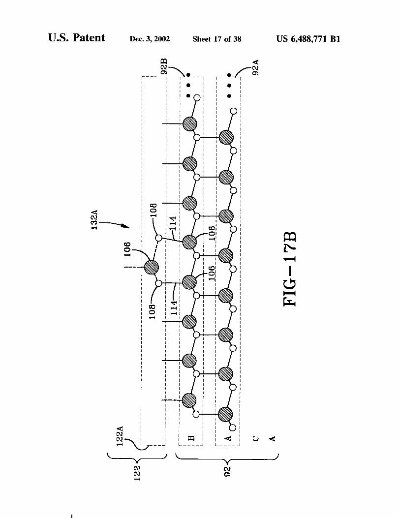
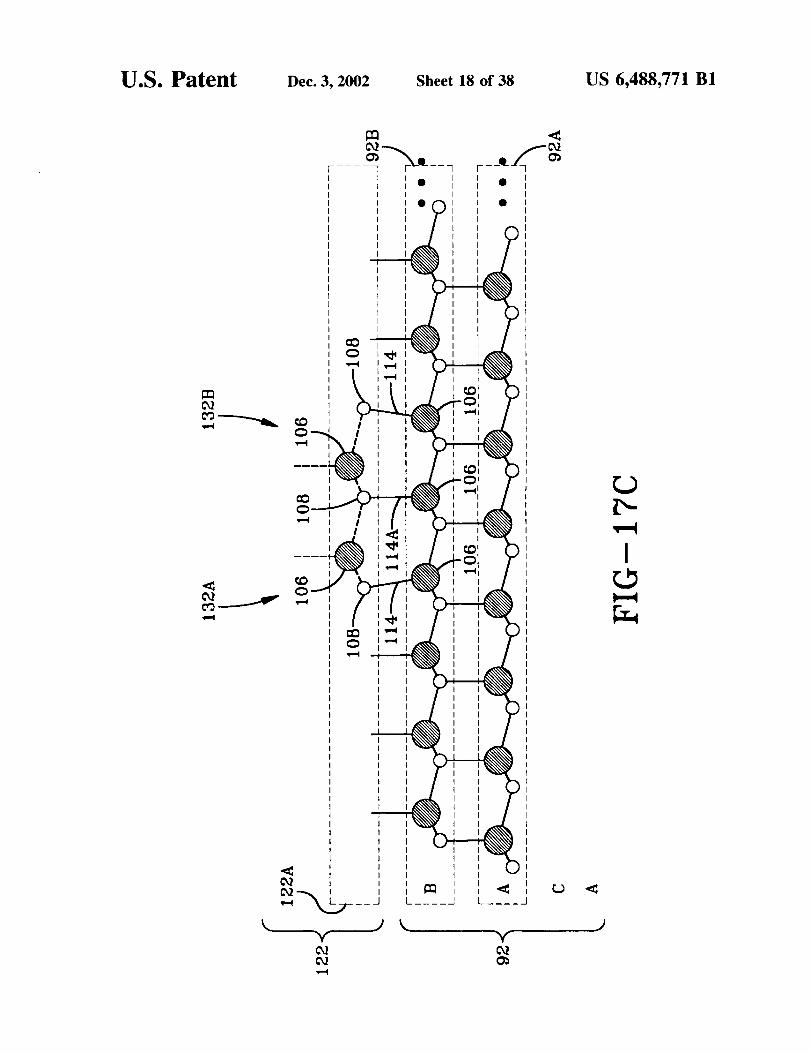
FIG. 17 is composed of FIGS. 17(A), 17(B), 17(C), and 20
17(D), wherein FIG. 17(A) illustrates the state of a step-free
4H-SiC surface prior to heteroepitaxial deposition, FIG.
17(B) illustrates a small initial two-dimensional (2D)
nucleus, i.e., bilayer comprised of one tetrahedral cell, FIG.
17(C) illustrates that the lateral position of the first tetrahe- 25dral cell of FIG. 17(B) has shifted, after further deposition
to incorporate a second tetrahedral into the bilayer island,
laterally slightly to the left as compared to that of FIG.17(B), and FIG. 17(D) illustrates the lateral position of the
first tetrahedral cell, as well as other tetrahedral cells of the 30
bilayer island, becomes anchored after sufficient number oftetrahedral cells have obtained their desired bonding.
FIG. 18 illustrates the bonding between the first layer in
the 3C-SiC bilayer and the upper layer of the 4H-SiCstructured polytype associated with leftward expansion of a 35
single anchored 3C-SiC bilayer island.
FIG. 19 illustrates the continuation of the bonding of FIG.
18 as the anchored 3C-SiC island expands via step-down
growth to the left.
FIG. 20 illustrates the completed bonding between the 40
first layer of the 3C-SiC film and the upper layer of the
4H-SiC substrate polytype without causing defects in the3C-SiC film.
FIG. 20A illustrates the undesired possible nucleation of 45opposite rotations of 3C-SiC on top of the step-free com-
pleted first heteroepitaxial bilayer.
FIGS. 21, 22, and 23 illustrate the prior art formation ofthe defective coalescence between two anchored 3C-SiC
islands, one expanding leftward and the other expanding 50rightward, causing a stacking fault defect.
FIGS. 24, 25. and 26 illustrates the slight (uncontrollable)
possibility of providing for a simultaneous growth betweentwo anchored 3C-SiC islands without the creation of any
defective coalescence that creates a defect. 55
FIG. 27 is composed of FIGS. 27(A) and 27(B) that
illustrate the growth of a second 3C-SiC bilayer on top of the
first 3C-SiC bilayer island in accordance with the practice of
the present invention.
FIG. 28 is composed of FIGS. 28(A) and 28(B) that 60
illustrate the nucleation and growth of two 3C-SiC second
bilayer islands on top of a completed growth of the first
bilayer th, t could result in crystal defect formation.
FIG. 29 is composed of FIGS. 29(A) and 29(B) that
illustrate the incoherent coalescence of two bilayer islands 65
that nucleated on the first heteroepitaxial bilayer; the result
is a double-positioning boundary (DPB).
B1
8
FIG. 30 illustrates a silicon crystal structure having manysimilar structural features of the 3C-SiC structure of FIG.
15(A), including stacking of tightly bonded bilayers and
tetrahedral bonding structure of nearest-neighbor atoms.
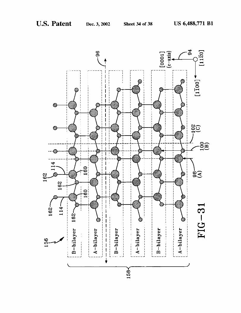
FIG. 31 illustrates a 2H-A1N structure having manysimilar structural features of the 4H-SiC structure of FIG.
14, including stacking of tightly bonded bilayers and tetra-
hedral bonding of nearest-neighbor atoms.FIG. 32 illustrates the different lateral atomic spacing of
bilayers of two materials, 2H-AIN and silicon, in theirnatural unstressed state.
FIG. 33 illustrates an atomically flat basal plane silicon
substrate surface prior to growth.
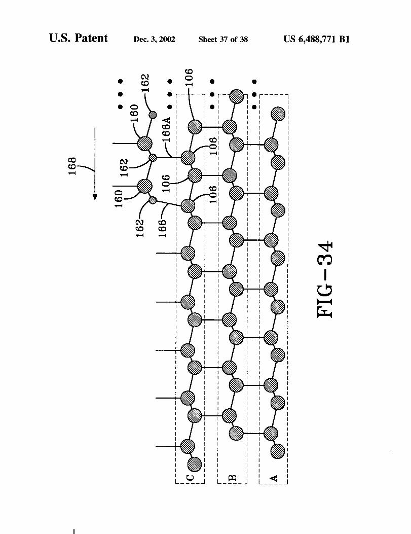
FIG. 34 illustrates leftward lateral step-flow expansion of
an AIN anchored bilayer having many of the salient features
of FIG. 18, with the exception that the substrate is silicon
(cubic) and the heteroepitaxial layer is AIN (hexagonal).
FIG. 35 is a continuation of the bonding of the film ofFIG. 34, wherein the lattice mismatch stress is relieved
along the basal plane, with the illustration of FIG. 35 having
many of the features of FIG. 20, but with the exception that
the dangling bond is from a heteroepilayer instead of fromthe substrate.
DETAILED DESCRIPTION OF THE
PREFERRED EMBODIMENTS
Referring now to the drawings, wherein the showings are
for the purpose of illustrating preferred embodiments of theinvention only and not for the purpose of limiting the same,
the invention describes an improved chemical vapor depo-
sition (CVD) method for obtaining improved quality of the
grown crystal films. Prior art chemical vapor deposition
(CVD) processes are disclosed in U.S. Pat. Nos. 5,463,978,5,915,194, 5,363,800, and 6,165,874, all of which are
herein, incorporated by reference. Other growth processes,
e.g., sublimation, physical vapor phase epitaxy, molecular
beam epitaxy (MBE), and others may be used in the practiceof the present invention. While the method may be applied
to many different crystals contemplated by the present
invention, the method will be primarily described with
respect to the growing of silicon carbide (SIC) crystals. The
improved CVD method includes pretreating a substrate,
heating the substrate in a reaction chamber, introducing a
carrier gas, vaporizing the crystal growing compounds,
introducing the vaporized compounds in the reaction cham-ber via the carrier gas and maintaining proper energy levelsand material flow rates in the reaction chamber for a
sufficient time to grow a crystal film having a desired smooth
surface morphology, a desired thickness, a low-defect den-
sity and a controlled impurity profile. The crystals may beintentionally doped to form n-type conductivity and/or
p-type conductivity crystals. As described in U.S. Pat. No.
5,915,194, the CVD crystal growing method provides for
atomically flat basal-plane surfaces grown by step-flowgrowth over a wide range of conditions provided that the SiC
substrate surface is properly prepared.
In general, the method of the present invention is related
to depositing a heteroepitaxial single-crystal film on a plu-
rality of step-free surfaces of a basal plane surface orienta-
tion of a selected single-crystal substrate material serving as
a wafer. The method comprises the steps of:
(a) preparing more than one step-free planar surface onthe selected substrate, wherein each of the plurality of
step-free surfaces has a boundary of selected size and
shape;
(b) selecting a heteroepitaxial film material whose chemi-
cal bonding structure is tetrahedral and exhibits a

US 6,488,771
9
property that under predetermined growth conditions
that growth of the heteroepitaxial film material growsin bilayers on the selected step-free planar surface;
(c) carrying out a selected deposition process under
selected growth conditions that produce (1) a single 5
nucleus of the heteroepitaxial film material at least one
bilayer thick on the step-free surface with the selected
boundary, followed by (2) lateral expansion of the
single nucleus over entire surface defined by the
selected boundary of the plurality of step-free basal l0plane surfaces before a second nucleus can form else-
where on the selected step-free planar surface, and (3)
a single nucleus of the second bilayer of heteroepitaxial
film, followed by (4) lateral expansion of the single
nucleus over the entire surface defined by the selected 15
boundary of the step-free basal plane surface before a
second nucleus can form elsewhere on the first bilayer
of heteroepitaxial film on the selected step-free planarsurface, and
(d) providing growth of subsequent additional bilayers of 20the said heteroepitaxial film by providing a suitable set
of growth conditions until a desired thickness of said
heteroepitaxial film is achieved.The method of the invention can be carried out with a
conventional chemical vapor deposition (CVD) system 25similar to that used in Si, SiC and GaAs semiconductor
technology. The gases used in a SiC CVD system are
hydrogen (used as a carrier gas), silane (used as a source of
Si), propane (used as a source of C), HC! (used for cleaning
and preparing the substrate surface), nitrogen (N2) (used as 30
a n-type dopant), and trimethyl aluminum (TMA) (used as
a p-type dopant). Other gases may be used as the Si or Csource or used to dope or etch the crystal. Gases other than
hydrogen and various gas mixtures can also be used as a
carrier gas. If organic compounds are used as the Si and C 35
sources, the process is commonly referred to as metal-
organic vapor phase epitaxy (MOVPE). Any CVD system
that can deliver these gases to a suitable reaction chamber atthe proper flow rates under high purity conditions and at the
proper substrate temperatures can be used for the method of 40
the present invention.
Referring now to FIG. 1, there is shown a schematic,
partial view of one suitable CVD reaction system for car-
rying out the process of the invention. The CVD reaction
system includes a reaction chamber 22 comprised of a 45
double-walled quartz tube such that the inner quartz tube can
be water-cooled. A SiC substrate 24 is supported by a SiC
coated graphite susceptor 26, which, in turn, is supported by
quartz support 28. To produce the desired temperature of the
surface of substrate 24, a radio-frequency (RF) induction 50
coil 30 is disposed around reaction chamber 22. Induction
coil 31) is powered by frequency generator 29. The RF field
produced by induction coil 30 heats substrate 24 via sus-
ceptor 26 to the desired temperature. When SiC film layers
are grown, substrate 24 is preferably a SiC substrate. The 55
gaseous crystal compounds are introduced into reaction
chamber 22 by primary line 33. Primary line 33 is located at
one end of reaction chamber 22 and directs the gases to flow
in direction G across substrate 24 and out the opposite end
of chamber 22. The various gaseous crystal compounds are 60
connected to primary line 33 and the gas flow is regulated by
valves 34 and regulators 35 connected to each gas line. Line36 is the silicon gas line that controls the silane flow into
primary line 33, and line 37 is the carbon gas line that
controls the propane flow into primary line 33. The dopants 65are introduced into primary line 33 by line 38 and line 39.
Line 38 is the n-type dopant line and preferably controls the
B1
10
nitrogen gas (N2) flow rate. Line 39 is the p-type dopant line
and preferably controls the trimethyl aluminum (TMA) flow
rate. Carrier gas line 31 carries all the gaseous crystalcompounds and dopants through primary line 33 and into
reaction chamber 22. The carrier gas is preferably hydrogen(He). Carrier gas line 31 is partially diverted into line 31a to
supply line 39 so that the carrier gas can be bubbled throughthe liquid TMA when p-type aluminum doping is desired. A
vacuum line (V) connected to a vacuum pump can beconnected to primary line 33 to evacuate reaction chamber22 of gases.
SiC substrate 24 is prepared by slicing a wafer sectionfrom a SiC boule. The SiC substrate 24 is chosen to be a
single crystal substrate material which exhibits a propertythat the material contains at least one growth plane orien-
tation whereby under selected growth conditions, to befurther described, the growth rate due to step-flow growth is
greater than at least one hundred (100) times the growth ratedue to growth involving two-dimensional nucleation, also tobe further described. Further, the single-crystal substrate 24
may be selected from the group of hexagonal type polytype
compositions consisting of 6H-SiC and 4H-SiC. In another
embodiment, the single-crystal substrate 24 may be of a
material that has a rhombohedral crystal structure and is
15R-SiC. Further, in an additional embodiment, the single-
crystal substrate 24 may be of a material that has a cubic
crystal structure and is selected from the group consisting of
silicon; germanium; SiGe: GaAs; and GaP.The tilt direction of the substrate 24 is sometimes selected
so as to produce the optimum growth rates and quality of theSiC epitaxial films grown on substrate 24. The surface of
substrate 24 is polished preferably on one surface with a
diamond paste and/or a final polish using a chemical-
mechanical polishing technique. As will be further
described, the step-free surface may have a (0001) crystal-
lographic orientation for hexagonal or rhombohedral crystal
structure materials, or the step-free surface may have a ( 111 )
crystallographic orientation for cubic crystal structure mate-rials.
Substrate 24 is cut such that the surface is slightly
misoriented relative to the basal plane by a tilt angle of less
than 1% Often, the tilt direction is preferably toward the
<1120> direction as illustrated in FIG. 2 to produce the
optimum growth rates and quality of the SiC epitaxial films
grown on substrate 24. SiC substrate 24 has three faces: aSi-face 50, a C-face 52, and the A-face 54. as illustrated in
FIG. 3. Preferably Si-face 50 is polished and used for
epitaxial growth. It has been found that Si-face 50 produces
the highest quality epitaxial layer films which have the best
surface morphology.
Substrate 24 is further prepared by creating boundaries of
trenches a2 on the face of substrate 24 which form growthregions 64) (also called mesas), as illustrated in FIG. 4.
Further, substrate 24 is further created to define a pluralityof mesas 61) to be used as to be further described. Trenches
62 forming growth region boundaries are preferably pro-
duced by photolithographically patterned reactive ion etch-
ing. However, boundaries 62 may be formed by other
physical means, such as, a precision dicing saw with a 25
micrometer thin blade, photolithography, laser etching, pho-
tochemical or electrochemical etching processes. The width
of trenches 62 need only be 10 micrometers, but larger or
smaller widths can also be used. The depth of trenches 62 ispreferably about 50 micrometers, but may be deeper or
shallower. Typically, an array of device-size regions, 200
micrometers×200 micrometers in size, is produced on the
substrate 24. Depending upon the density of substrate
defects, other sizes, larger or smaller, can be produced.

US 6,488,771 B 1
11
Once the substrate surface has been polished and growth
regions (i.e., mesas) 60, substrate 24 is pretreated to removecontaminants or impurities on the surface of the substrate so
as to facilitate the growing of high quality, low-defectepitaxial films. Various ex-situ pregrowth treatments, such
as oxidation, chemical mechanical polishing, or reactive ionetching may be used to remove potential unwanted nucle-
ation sites prior to growing the crystal epilayers. Thensubstrate 24 is placed in reaction chamber 22. Prior togrowing the crystal film layers on substrate 24, the substrateis pretreated with an in-situ pregrowth process to removeremovable contaminants and defects on the surface of thesubstrate 24 that could act as unwanted sites for two-dimensional nucleation of the SiC film layers. These defects
on the surface of the substrate can be generated during thecutting and polishing of the substrate. Preferably, the pre-
growth process involves subjecting substrate 24 to a hightemperature gaseous etch in a hydrogen gas, sometimes
mixed with hydrogen chloride gas, within the reactionchamber 22. The pregrowth process is such that the substrate
is not altered in a way that unwanted sites for two-
dimensional nucleation are produced on the surface of the
substrate. Preferably, the etch uniformly removes materialfrom the surface of substrate 24 to ensure a low-defect,
highly-pure surface. Further details of the desired etch maybe found in U.S. Pat. No. 5,915,194, as well as in a technicalarticle "Process-Induced Morphological Defects in Epitaxial
CVD Silicon Carbide" by J. A. Powell and D. J. Larkin,
published in Physica Status Solidi (b), vol. 202, no. 1, pp.529-548 (1997).
Once substrate 24 has been pretreated, reaction chamber
22 is prepared for crystal growth. Reaction chamber 22 is
preferably evacuated by vacuum via vacuum line V and
subsequendy purged with an inert gas to remove impurities.
Hydrogen gas may be used to purge the reaction chamber.Once the reaction chamber is purged, the carrier gas flowrates and the temperature within the reaction chamber are
brought to equilibrium. Hydrogen gas is preferably used as
the carrier gas, but other gases (e.g., inert gases) can be used.
Once the temperature and flow within the reaction chamber
22 have reached equilibrium, generally within less than one
minute, silane and propane are added to the carrier gas to
initiate SiC growth. Preferably, the silane concentration
within the career gas is approximately 200 ppm resulting in
a 200 ppm atomic concentration of Si. Preferably the amount
of propane introduced into the carrier gas is approximately
130 ppm to 600 ppm resulting in an atomic concentration of
C between 390 ppm to 1800 ppm. The prescribed pretreat-ment of substrate 24 allows for significantly greater devia-
tions from the optimum Si/C ratio than was previously
thought possible for growing high-quality, low-defect SiC
crystals. The ratio of the atomic concentrations of Si to C
may be varied to create different growth rates and different
growth conditions for SiC epilayers. The ratio may rangebetween 0.1 and 0.8.
The first phase of crystal growth forms a step-free basal
plane surface in a manner consistent with the teaching ofU.S. Pat. No. 5,915,194 and can be described by referring
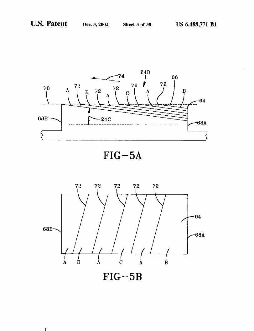
now to FIG. 5, which is composed of FIGS. 5(A) and 5(B).FIG. 5(A) shows, in cross-section, a typical mesa etched into"on-axis" SiC wafer 24D that has been polished and is
oriented within a small tilt angle 24C relative to the crystal
(0001) plane (also called the basal plane) identified byreference number 66 in FIG. 5(A). The surface has been
etched to define a mesa with edges 68 comprised of a first
or right edge 68A (as viewed in FIG. 5(A) as well as other
FIGS herein) and a second or left edge 68B (as viewed in
FIG. 5(A) as well as other FIGS herein).
12
As will be further described, each SiC crystal is formed
from the SiC wafer 24D by a specific stacking sequence of
bilayers of tightly bonded Si and C atoms. Each of theselayers has a basal plane 66. Hereinafter, the top most layer
5 of the SiC crystal surface within an etched mesa having
edges 68 is termed the initial plane 64 shown in is FIG. $(A).The SiC wafer 24D has an initial top surface 70. Because of
the unintentional small angle tilt of the top surface 70 with
respect to the basal plane 66, surface steps 72 are formed at
10 the surface. The SiC crystal growth direction shown in FIG.
5, is a lateral growth (i.e., stepflow growth) in a direction
indicated by directional arrow 74.
FIG. 5(B) is a top view of FIG. 5(A) and primarily
illustrates the initial steps 72 prior to epitaxial growth. More
15 particularly, FIGS. 5(A) and 5(B) primarily show the state of
the SiC wafer 24D before it is provided with an atomically
flat surface which may be further described with reference toFIGS. 6(A) and 6(B).
FIG. 6(A) is quite similar to FIG. 5(A). but illustrates the
20 elimination of the surface steps 72 following sutficient
stepflow epitaxial growth without two (2) dimensional
nucleation in a manner more fully described in U.S. Pat. No.
5,915,194.FIG. 6(A), as well as FIG. 5(A), for one embodiment
25 illustrates a 4H-SiC stacking order A, B, A. C, however, both
FIGS. 5(A) and 6(A) could have utilized a 6H stacking order
A, B, C, A, C, B, or other stacking orders for other SiC
polytypes. FIG. 6(B) is a top view of FIG. 6(A) andillustrates that the top surface 66 is smooth and, more
30 particularly, is an atomically flat surface completely free of
steps and serves as a starting growth surface for the presentinvention.
The heteroepitaxial film selected for the practice of the
present invention may be of various materials, such as a
35 single-crystal film having a hexagonal crystal structure and,in some embodiments, is selected of a material different
from the substrate 24, with the different material being
selected from the group consisting of 2H-SiC; 2H-GaN:
2H-AIN; 2H-A1GaN; and 2H-InGaN. The heteroepitaxial
40 single-crystal film may also have a cubic crystal structure
and, in some embodiments, is selected of a material differentfrom the substrate 24 material and is further selected from
the group consisting of silicon, germanium, SiGe, diamond,
3C-SiC, GaAs. AlAs, AIGaAs. InAs, InP, lnGaAs, Inp,45 lnGaAsP, cubic-GaN, cubic-AIN, Cubic-A1GaN, cubic-
lnGaN. When the selected substrate 24 material is
hexagonal-SiC, the heteroepitaxial film material may be3C-SiC. When the single-crystal substrate 24 material is
hexagonal-SiC, the heteroepitaxial film material may be50 diamond. When the single-crystal substrate 24 material is
hexagonal-SiC, the heteroepitaxial film material may be a
III-N alloy.The method of the present invention related to the growth
of heteroepitaxial films is different than that of U.S. Pat. No.55 5,915,194. More particularly, U.S. Pat. No. 5,915,194 pro-
vides for multiple heteroepitaxial growth islands, whereas
the present invention provides for optimum growth (i.e.,
defect-free) by requiring a first bilayer to complete its lateral
step-flow growth expansion of a single heteroepitaxial
60 nucleation island of the heteroepitaxial film on the atomi-
cally flat surface provided by the homoepitaxial film of
FIGS. 6(A) and 6(B) before any growth of any other
nucleation island is allowed to begin elsewhere on the
atomically-flat homoepitaxial film surface. The present
65 invention also provides for optimum growth (i.e. defect free)
by requiring a second bilayer to complete its lateral step-
flow growth expansion of a single heteroepitaxial nucleation

US 6,488,771 B1
13
island of the second heteroepitaxial bilayer on the surface
provided by the first bilayer of the heteroepitaxial film. The
growth of the nucleation island related to the present inven-
tion is herein referred to as a 3C-SiC bilayer island because,
as will be further described, 3C-SiC is the SiC polytype thatforms when two dimensional (2D) terrace nucleation occurs
during SiC epitaxy. The heteroepitaxial film growth of the
present invention may be further described with reference toFIG. 7 composed of FIGS. 7(A) and 7(B), wherein in FIG.
7(B) is a top view of FIG. 7(A).
FIG. 7(A), as well as FIGS. 8(A), 9(A), 10(A), ll(A),27(A), 28(A), and 29(A), is a cross-sectional view of the
mesa at various stages, to be described, of heteroepitaxial
growth. The stacking arrangement (B, A, C, A, B illustrated
for 4H-SiC) 76 of homoepitaxial film is shown. FIGS. 7(B),
8(B), 9(B), 10(B), II(B), 27(B), 28(B), and 29(B), respec-
tively illustrate top views of FIGS. 7(A), 8(A), 9(A), 10(A),II(A). 27(A), 28(A), and 29(A).
It is well known to those skilled in the art that when 2D
terrace nucleation occurs instead of step-flow during SiC
epitaxial growth on a hexagonal SiC substrate, the stackingorder becomes 3C-SiC. This is discussed in U.S. Pat. No.
5,915,194 and references therein. Thus, when growth con-
ditions permit 2D nucleation on the step-free surface, which
is in effect a large basal plane terrace, the bilayer takes on the
3C-SiC stacking sequence.FIG. 7(A) illustrates the formation of an initial 3C-SiC
island 78A that is laterally expanding in the directionsindicated by directional arrows 80. It should be noted that
the 3C-SiC bilayer island 78A is a double layer of tightlybonded Si and C atoms. FIG. 7(B) further illustrates the
initial 3C-SiC bilayer island 78A. The lateral enlargement ofthe 3C-SiC bilayer island 75A via step-flow growth may befurther described with reference to FIG. 8 which is com-posed of FIG. 8(A) and 8(B).
The initial 2D nucleation of the 3C-SiC bilayer island 78Ais accomplished by conditions that barely promote limitedtwo-dimensional (2D) nucleation, in addition to the condi-
tions that provide step-flow growth on the atomically flatepilayer surface 66. The conditions that begin to increasetwo-dimensional nucleation include a lower growth tem-perature and/or higher concentration of silane and propaneand/or higher Si/C ratios to be further described. Once the
3C-SiC bilayer island 78A is nucleated, lateral expansion ofthe 3C-SiC bilayer island 78A takes place via stepflow
growth.
As seen in FIG. $(B) the first 3C-SiC bilayer island 78Agrows laterally to reach the first edge 68A of the mesalocated on the right hand side as viewed in FIG. 8(A) and
FIG. 8(B) and continues to grow in direction 80 toward thesecond edge 68B, located on the left hand side as viewed inFIG. 8(A) and FIG. 8(B). The desired _owth of the first3C-SiC bilayer island 78A is best seen on FIG. 8(B). The
direction of growth 80 shown in FIG. 8 is also applicable toFIGS. 9, 10, and 11.
As seen in FIG. 8(B), the first and only 3C-SiC bilayerisland 78A has completed approximately two-thirds of itsgrowth covering the top surface 66 (which has the B positionin the stacking order). The completion of the lateral expan-sion growth of the first 3C-SiC island 78A may be furtherdescribed with reference to FIG. 9 composed of FIGS. 9(A)and 9(B).
As seen in FIG. 9, the first and only 3C-SiC bilayer island78A has completed its growth over the entire step-free mesasurface before any additional island is allowed to nucleate
on the original step-free surface 66. The state of growth
shown in FIG. 9 provides the first bilayer 82 of the 3C-SiC
14
polytype. As seen in FIG. 9(B), the first 3C-SiC bilayer
island 78A has grown over the entire atomically fiat surface
66 and is defect-free. This can be done, in situ, during the
growth that provides the initial heteroepitaxial growth that
5 allows the first 3C-SiC bilayer island 78A to nucleate and
grow laterally by step-flow across the entire atomically fiat
surface before a second 3C-SiC bilayer island can nucleate
on the atomically flat surface. Thus, proper control of theinitial 3C-SiC bilayer island 78A nucleation rate on the
t0 atomically flat surface is necessary for at least the first
bilayer in order for this to occur. Proper control of the initial
nucleation rate is accomplished by selecting proper growth
conditions at the initiation of the heteroepitaxial growth ofthe 3C-SiC bilayer island 78A. A combination of factors that
15 affect the nucleation rate (and therefore the probability ofachieving a single-initial-island nucleation of the 3C-SiC
bilayer island 78A) include (but are not necessarily limited
to) growth temperature, growth pressure, growth flow,growth precursor concentrations, intentional and uninten-
20 tional impurities. As will be further described below, the
selection of proper nucleation rate is related to the size and
shape of individual step-free mesa surfaces. The growth
conditions of the present invention comprise a set of growthparameters comprising at least substrate temperature, reactor
25 pressure used for the deposition, concentration of reactor
precursors for material being deposited, composition of
carrier gas used within the reactor, and flow rate of carrier
gas within the reactor. For example, in silicon carbide, it is
well known to those skilled in the art, that as the growth
30 temperature is reduced, the probability of 3C-SiC bilayerisland nucleation (such as 78A) increases as described in the
technical article "Nucleation and Step-Motion in Chemical
Vapor Deposition of SiC on 6H-SiC {0001 } Faces" by T.
Kimoto and H. Matsunami, published in J. Appl. Phys., vol.35 76, pp. 7322-7327 (1994). It has also been observed on SiC
growth surfaces with steps that increasing the concentration
of silicon precursors increases the nucleation of 3C-SiC
bilayer island 78A. For any given island nucleation rate(related to the 3C-SiC bilayer island 78A) that results from
40 selected growth conditions, the size and shape of the mesa,
such as mesa 68, can be optimized to help maximize theprobability of achieving the desired single-initial-island,
such as 3C-SiC bilayer island 78A, nucleation and complete
lateral expansion via step-flow growth being accomplished45 without having a second 3C-SiC bilayer island nucleate on
the step-free mesa surface 66 prior to the complete coverageof the mesa. In cases where the SiC wafer 24D has diverse
lateral sizes and shapes of step-free mesas on its top surface,it has been discovered that it is possible to achieve the
50 desired single-island initiation and bilayer coverage of bet-
eroepitaxial growth by gradually changing the growth con-
ditions starting from low nucleation rates (suitable for the
largest step-free mesas), to higher nucleation rates (suitable
for the smaller step-free mesas), as a function of time.
55 Experimental evidence indicates that the shape of the mesa
also impacts the rate of nucleation. For example, we have
observed that the rate of the two dimensional (2D) nucle-
ation related to the 3C-SiC bilayer islands of the presentinvention is greater for a square mesa shape than for a
60 narrow rectangular mesa shape of equivalent mesa surface
area. We believe this is due to depletion-of surface reactants
near the mesa edge due to growth on the side of the mesa
because growth reactants readily incorporate into A-face(see reference number 54 of FIG. 3) mesa sidewall. Further
65 details of the mesa shapes are to be further described with
reference to FIG. 13. The benefits of the present invention
may be better appreciated by a general discussion of the

US 6,488,771 B 1
15
disadvantages of the prior art that allowed a second nucle-ated island (such as, 3C-SiC bilayer island 78B) to begin its
growth on the step-free mesa surface 66 before the comple-tion of the first 3C-SiC bilayer island 78A and may befurther described with reference to FIG. 10, which is com-
posed of FIGS. 10(A) and 10(B).FIG. 10 illustrates that before the first 3C-SiC bilayer
island 78A has completed its growth across the entire upper
atomically flat surface of the mesa 66, the nucleation andlateral growth of a second 3C-SiC bilayer island 78B has
been initiated at another place on the flat surface 66. As seenin FIG. 10(A), the first 3C-SiC bilayer island 78A has grown
from the right edge 68A and is pursuing its growth indirection 80A toward the left edge 68B, but has not yet
merged with the second growing 3C-SiC bilayer island 78B,which is more clearly shown in FIG. 10(B).
As seen in FIG. 10(B), the first 3C-SiC bilayer island 78A
is expanding toward, but has not intercepted the secondgrowing 3C-SiC bilayer island 78B. The further lateral
step-flow growth of both first and second 3C-SiC bilayerislands 78A and 78B, respectively may be further described
with reference to FIG. 11 which is composed of FIGS. IliA)
and IIIB).
As seen in FIG. ll(A) the first 3C-SiC bilayer island 78A
has grown laterally toward and has intercepted a portion ofthe second 3C-SiC bilayer island 78B (which has also stepflow grown laterally) so as to create a point 84 of incoherentcoalescence, which may be further described with reference
to FIG. ll(B).Unless one is extremely fortunate, as described later with
reference to FIGS. 24-27, incoherent lateral coalescence is
likely to occur at point 84, shown in FIG. ll(B) resulting ina first stacking fault defect with continued growth formingfault 84A shown in FIG. 12. The physical reasons forincoherent coalescence are to be described later with refer-
ence to FIGS. 16, 17, and 20-23. If yet more islands, that is,3C-SiC bilayer islands, nucleate (i.e., a third or fourth3C-SiC island) on the fiat mesa surface 66, there will be evenmore incoherent coalescence and, thus, even more stacking
fault defects initiated in the heteroepitaxial film.The selected deposition process of the present invention
comprises carrying out deposition under selected growthconditions over a selected period of time to produce an
average rate of nucleation (NRI) and an average velocity of
lateral island expansion (VLEI) for the growth of the first
heteroepitaxial bilayer and an average rate of nucleation
(NR2) and an average velocity of lateral expansion (VLE2)
for the growth of the second heteroepitaxial bilayer.
Preferably, there are multiple selected growth conditions
that are carried out in a sequential manner. More particularly,
it is preferred that the growth conditions be selected so as to
sequentially increase the average nucleation rate of each
growth condition carried out in a sequential manner.
Specifically, it is preferred that the sequential increases of
the average nucleation rate be accomplished in a staircase or
ramp manner.As is known to those skilled in the art, different growth
conditions lead to different amounts (i.e., rates) of two-
dimensional (2D) island nucleation during epitaxial growth.
For example, it is well known to those skilled in the art that
the rate of 2D island nucleation of 3C-SiC can be affected by
epitaxial growth temperature. However, until this invention,to our understanding, it has not been appreciated or under-
stood that a very specific of nucleation rate window is
necessary for improved heteroepitaxial growth on atomi-
cally flat surfaces. The discussion below details the relevantcharacteristics of one particular "growth condition window"
desired to practice the present invention.
16
Assume that we have a properly prepared, in a manner as
previously described, substrate serving as a wafer in a
suitable epitaxial growth reactor with an array of atomically
flat surfaces ready for nucleation and growth of a heteroepi-
5 taxial film. Next, assume the wafer is patterned with an array
of rectangular step-free mesa surfaces, each with the same
area A and length dimension L and width dimension W. For
this simple case A (cm2)=L (cm)×W (cm). A top view of onesuch a mesa 66 is shown in FIG. 13A. Next, assume the need
10 to select a time invariant heteroepitaxial growth condition
that will give us the desired growth result, namely, single-
island nucleation of ( 1_first heteroepitaxial bilayer followed
by expansion to the edge of the mesa 66 prior to a second
island nucleating on the step-free surface in a manner as
15 already discussed, and (2) the single-island nucleation fol-lowed by expansion of a second heteroepitaxial bilayer on
top of the first bilayer prior to the second island nucleating
on the first bilayer surface.
For given time-invariant growth conditions, atomically20 fiat substrate material, and heteroepitaxial material, there is
a time-invariant average rate of 2D island nucleus formation,
hereafter referred to as the nucleation rate (NR), given in
units of [# of nucleationsl/[unit area (cm2)xunit time (sec.)].
There is also an average velocity of lateral expansion (VLE)
25 of a nucleated island across the step-free mesa 66, given in
units of [unit distance (cm)l/[unit time (sec.)]. The average
velocity of lateral expansion (VLE) is indicated in FIG. 13A
by directional arrows 86 emanating from a nucleated island78E.
30 For the given step-free mesa 66 size with a given top
surface area A subjected to the above growth conditions, the
number of nucleations on average that will occur every
second is given by:
35 NS=NR'/,Ain units of [# of nucleations]/[time(sec)].
ThUS the average time between 2D island nucleations
(T2D) for this mesa 66 size under these growth conditionsis:
40 T2D=I/NS in units of time (sex).
Once an island 2D nucleates on the step-free surface, the
present invention teaches that it is desired that the island,such as island 78E of FIG. 13A, grow laterally to cover the
45 farthest edge of the mesa before a second nucleation can takeplace on the original step-free surface. If an island 2D
nucleates at one extreme end of the step-free mesa. and
laterally expands at the VLE velocity defined above, thetime it would take for the entire mesa to be covered (TC)
would be:50
TC=I.JVLEin units of time (sec).
where L is the length of the mesa 66 and VLE is the
island's velocity of lateral expansion (VLE) discussed55 above. This represents a worst-case coverage time
(TC), dnce the distance of lateral expansion needed tocover the island would be L/2 if the island nucleated in
the middle of the mesa.
For the present invention to be preferably practiced in this
60 case (i.e., for single-island nucleation and expansion to be
accomplished prior to a second island nucleating on the
step-free substrate surface), growth conditions should be
selected so that the average time between 2D island nucle-
ations (T2D) is larger than the coverage time (TC) and
65 which may be expressed as follows:
T2D>TC

17
which by mathematical substitution from previous equa-tions can be expressed as:
1 L
(NR)(A) > VLE
which can be algebraically rearranged as:
VLE-- > (L)(A)NR
When the growth conditions and mesa 66 size and shape
are in the window that satisfies the above inequality, thepresent invention will be accomplished on the majority of
step-free mesas of top surface area A arrayed on the sub-strate.
For the practice of the present invention, it is also desired
that the majority of step-free mesas undergo 2D nucleation
followed by complete mesa coverage needed to accomplish
the heteroepitaxy of the present invention. As will be further
described, it is desired that single-island nucleation and
mesa coverage occur for the first two bilayers of heteroepi-taxial film. Therefore, the amount of time that the above
growth conditions are maintained (TG) must exceed the sum
of the nucleation time (T2D) and the coverage time (TC) forthe first two bilayers:
TG> T'2D+ TC
For a more general mesa shape than a simple rectangle,
there is not necessarily a simple straight-line length. We
therefore must more accurately define the "L" term in the
above inequality as the total distance that a nucleus at one
end of the mesa shape would have to traverse to the most
distant opposite end of the mesa shape. An example 88 of
this accumulated planar length LA is illustrated for an
L-shaped mesa in FIG. 13B showing the quantity LA=LI+L2.
As used herein, the quantities NR, VLE, T2D, and TC fora first heteroepitaxial bilayer are designated as NR1, VLE1,
T2D1, and TC1, respectively. Similarly, the quantities NR,
VLE, T2D, and TC for a second heteroepitaxial bilayer are
designated as NR2, VLE2, T2D2, and TC2, respectively. Aswill be further described with respect to FIG. 27, the
distinction is necessary because NRI is not necessarily equalto NR2, and likewise VLE1 is not necessarily equal toVLE2. In particular, for cases where the chemical compo-sition of the heteroepitaxial material is different than the
chemical composition of the substrate material, it is unlikelythat NRI will equal NR2.
The growth conditions and the planar step-free planarsurface size and shape are selected such that the averagevelocity of lateral island expansion (VLEI) divided by the
average rate of nucleation (NR1) for the first bilayer and the
average velocity of lateral island expansion (VLE2) divided
by the average rate of nucleation (NR2) for the second
bilayer are both less than the product of a planar area (A) ofthe step-free planar surface multiplied by the longest planaraccumulated length dimension (L a) of the selected step-freeplanar surface.
The selected period of time is greater than the sum of the
following:
(i) the mathematical inverse of the product of the planar area(A) of the selected step-free planar surface multiplied bythe average rate of nucleation (NR1) with the result
thereof being termed T2D1;
US 6,488,771 B 1
18
(ii) the quotient of the longest planar accumulated length
dimension (La) of the selected step-free planar surfacedivided by the average velocity of lateral island expansion
(VLEI) with the result thereof being termed TC1;
5 (iii) the mathematical inverse of the product of the planar
area (A) of the selected step-free planar surface multiplied
by the average rate of nucleation (NR2) with the result
thereof being termed T2D2;
(iv) the quotient of the longest planar accumulated length
l0 dimension LA) of the said selected step-free planar surface
divided by said average rate of lateral island expansion
(VLE2) with the result thereof being termed TC2.
In order to more fully appreciate that the practice of the
present invention provides for the growth of multiple het-
15 eroepitaxial films that are free of stacking faults, a moredetailed discussion of lateral coalescence of the first two
bilayers of the heteroepitaxial film will be described withreference to FIGS. 14--26.
In general, in the practice of the present invention, and in
20 a manner known in the art, the crystallographic planeparallel to the bilayers, such as layer 82, is called the basal
plane. It is well known that the SiC polytypes grow by the
stacking of SiC bilayers. In accordance with the principlesof the present invention, and as known in the art, each silicon
25 and carbon atom within a given bilayer is bonded to three
other atoms within the same bilayer, and is only bonded by
a single bond to the adjacent bilayer. The bonding is thenatural physical force or interactions that cause atoms in a
single crystal to be held together in a well-ordered solid30 crystal structure. Therefore, each atom is much more
strongly (or tightly) bonded within its own bilayer than to
the adjacent bilayer. For this reason, the basal plane of the
SiC is considered the low energy "'slip" plane that is most
easily deformed and subject to dislocation propagation. The
35 principles of the present invention may be further describedwith reference to FIGS. 14-26 that illustrate the atomic
structure and bonding parameters and defects generated
during various cases of 3C-SiC heteroepitaxial growth on a
4H-SiC atomically-fiat mesa. These drawings (FIGS.40 14-26) and dimensions are not quantitatively accurate, but
are intended for purposes of illustrating basic principles ofthe present invention.
FIG. 14 illustrates a cross-sectional atomic representation
90 of a 4H-SiC crystal. The ABAC stacking arrangement 9245 of the different A B C bilayers is evident. FIG. 14 also
illustrates a Miller diagram 94 showing crystallographic
orientation related to crystal structure and known to thoseskilled in the art.
The 4H-SiC structure arrangement 90 has a basal plane50 (0001) 96. The horizontal position of the silicon atoms in the
4H-SiC structure corresponding to an A, B, or C bilayer is
respectively indicated by dimensional lines 98, 100, 102 also
respectively identified as (A), (B) and (C) which is repre-
sentative of the lateral position of the atoms corresponding
55 to the stacking order of the bilayers. This representation (AJ.
(B) and (C) of the lateral position is used throughout theillustrations herein and is to be further described hereinafter
with reference to FIG. 20(A). The stacking direction 104 is
perpendicular to the (0001) basal plane 96. The silicon
60 atoms are identified in FIG. 14 by reference number 106,
whereas the carbon atoms are identified by reference number108. Each atom has four covalent chemical bonds t o its
nearest neighbor atoms, wherein the bonds are shown as
110, 112, and 114. Bonds 112 and 114 are single bonds in the
65 plane of the figure. The third and fourth bonds are repre-
sented by 110 and are not in the plane of FIGS. 14, 15(A),
16-26 and 30-35. The bonds between adjacent bilayers of

US6,488,771B 119
the stacking arrangement 92 is generally identified by ref-
erence number 114, whereas a dangling bond (i.e., a bond
with no crystal atom on one end) possible at the surface of
the crystal is generally identified with the reference number118.
The cross-sectional atomic representation of 3C-SiC crys-
tal structure 120 may be further described with reference to
FIG. 15 composed of FIGS. 15(A), 15(B), and 15(C).
FIG. IS(A) illustrates two of the bilayer stacking direc-tions 126 and 130 of the four equivalent bilayer stacking
directions arrangements 122 of the A B C bilayers associatedwith the 3C-SiC structure arrangement 120. Unlike the
single bilayer stacking direction of the 4H-SiC structure of
FIG. 14, the cubic symmetry of the 3C-SiC structure 120 has
four equivalent basal planes each having associated there-
with a perpendicular bilayer stacking direction. It is wellknown in the art that in 3C-SiC (and other cubic structure
semiconductors), the basal plane is associated with (111)
Miller indices (also known in the art). However, for the sake
of clarity, and the confinement of the Figure to two
dimensions, FIG. 15(A) only illustrates a first (111) basal
plane 124 having a first stacking direction 126 and a second
symmetrically equivalent (111) basal plane 128 having a
stacking direction 130. The first and second stacking direc-
tions 126 and 130, respectively, are respectively perpendicu-
lar to basal planes 124 and 128.
FIG. 15(A) also illustrates dimensional lines 98, 100, and
102 illustrating the lateral positions of the silicon atoms 106
respectively in the A B C bilayers associated with stackingdirection 126, similar to that described with reference to
FIG. 14, but in addition thereto illustrates dimensional lines
98A, 100A, and 102A illustrating the lateral positions of thesilicon atoms 106 associated with the second depicted
equivalent stacking direction 130. In order for any volume
of 3C-SiC crystal to be free of stacking disorder (i.e. free of
stacking faults), the ordered atomic positions of the
ABCABC stacking must be maintained in all four (4)
equivalent stacking directions.
The bonding related to all SiC polytypes including 4Hillustrated in FIG. 14, as well as in 3C illustrated in FIG.
15(A) may be further described with reference to FIG.15(B). The bonding, known as tetrahedral, of SiC is gener-
ally illustrated in FIG. 15(B). As seen in FIG. 15(B), each
silicon atom 106 is bonded to four (4) nearest neighbor
atoms (carbon atoms 108 in the case of SIC). The nearest
four (4) neighbor carbon atoms 108 in the crystal lattice
form the points of a tetrahedron configuration, identified in
phantom by reference number 132, that encloses the silicon
atom 106. The configuration 132 is also referred to herein asa tetrahedral cell 132.
The bonding, also known as tetrahedral, of a silicon
crystal, to be further described with reference to FIG. 31, is
generally illustrated in FIG. 15(C). As seen in FIG. 15(C),each silicon atom 106 is bonded to four (4) nearest neighbor
silicon atoms 106. The nearest four (4) atoms form the points
of a tetrahedron configuration, identified in phantom byreference number 134, that encloses the selected silicon
atom.As discussed in "Growth and Characterization of Silicon
Carbide Polytypes for Electronic Applications," by J. A.Powell, P. Pirouz, and W. J. Choyke, Chapter 11 in Semi-
conductor Interfaces, Microstructures and Devices: Prop-
erties and Applications, Edited by Z. C. Feng, Institute of
Physics Publishing, Bristol, pp. 257-293 (1993), all SiCpolytypes have tetrahedral bonding configuration, as do
most semiconductor crystals. As shown in FIG. 15(B), 3 of
the 4 of the nearest-neighbor carbon atoms of a silicon atom
2Oin a tetrahedral cell can be used to define a plane that is a
monolayer (i.e., a carbon monolayer for FIG. 15(B)) of
crystal atoms. For 3C-SiC, the four possible monolayer
planes of the tetrahedral cell are parallel to the four possible5 basal planes described with reference to FIG. 15(A). For the
remaining SiC polytypes (such as 4H-SiC) with only one
basal plane, one of the carbon monolayer planes is parallelto that basal plane. For tetrahedral bonding arrangement,
growth parallel to the monolayer plane takes place in a
l0 bilayer fashion largely because atoms within the one (e.g.,carbon for SiC) monolayer plane cannot bond directly with
each other, but instead require simultaneous bonding and
propagation of a companion second (e.g., silicon for SiC)monolayer. Thus, growth along the basal plane of tetrahe-drally bonded crystals takes place in bilayers even for the
15 case of elemental semiconductor such as silicon. The tetra-
hedral bonding arrangement also leads to the necessary tight
bonding within bilayers, as 3 of the 4 nearest neighbor bondswill be with atoms within a given bilayer, leaving the fourthbond of the tetrahedral cell for bonding to an adjacent
20 bilayer.
The formation of stacking faults related to the presentinvention and the stressed and unstressed conditions of the
heteroepitaxial layer used in the practice of the present
invention, may be further described with reference to FIG.25 16.
FIG. 16 illustrates the natural unstressed condition of a
3C-SiC bilayer 136 and the unstressed condition of a
4H-SiC bilayer 138. From FIG. 16, it is seen that the lateralpositions of the silicon 106 and carbon 108 atoms between
30 bilayers 136 and 138 are offset from each other for the vastmajority of atoms. The different lattice spacing of the twomaterials (3C-SiC and 4H-SiC) in an unstressed state means
that the atoms thereof will not line up laterally when
vertically joined in heteroepitaxy. Different lateral spacing35 between the 3C and 4H bilayers arises due to the different
complete stacking sequences, even though the atomic spe-cies are the same in both cases. The phenomena of differentlattice spacing in SiC due to changes in the stacking
sequence is discussed in the technical article "Refinement of40 the Crystal Structure of SiC Type 6H," by A. H. Gomes de
Mesquita in Acta Crystallographica, volume 23, pp.610--617 (1967).
For purposes of illustration, the difference in lateralspacing is greatly exaggerated in FIG. 16 and subsequent
45 figures. In FIG. 16, the lateral spacing of six (6) C-atoms in
unstressed 3C-SiC bilayer 136 is depicted to be the same asseven C-atoms in unstressed 4H-SiC bilayer 138. Thus,lateral lattice mismatch illustrated in FIG. 16 is about equal
to the quantity of (1-(6/7)) (100)=15.3 percent. The actual50 lattice mismatch of 3C-SiC to 4H-SiC has been measured to
be around a few tenths of a percent. The exaggerated lattice
mismatch is necessary to illustrate important principles ofheteroepitaxy in the figures that are small enough to bedrawn and understood for the practice of the present inven-
55 tion. Otherwise, exceedingly complex figures with thou-
sands of atoms would have to be presented. For this case 3C
has lateral spacing larger than 4H, but the process works
even if the opposite relationship is true, as will be describedlater with reference to FIGS. 33-35.
60 The 4H-SiC stacking arrangement 92 illustrating the top
two bilayers 92A and 92B of an atomically-flat surface 66
prior to heteroepitaxy is shown in FIG. 17(A). As seen inFIG. 17(A), the bonds 114, between adjacent bilayers illus-
trate vertical alignment between the silicon atoms 106 in
65 bilayer 92A and the carbon atoms 108 in bilayer 92B.
Before reviewing the desired bonding as achieved by the
present invention starting with reference to FIG. 18, a brief

US 6,488,771 B 1
21
review of the principles of bonding of a small (2D) nucle-
ation may be further described with reference to FIGS.17(B), 17(C), and 17(D), wherein each show the first atoms
forming a small island nucleus of a first 3C-SiC bilayer122A of the stacking arrangement 122.
FIG. 17(B) illustrates a very small initial two dimensional
(2D) nucleus comprised of one (1) tetrahedral cell 132A thathas bonded to the step-free substrate surface 66. This initial
2D nucleus does not have enough vertical bonds 114 to have
its position laterally fixed with respect to a step-free sub-
strate surface 66 on which the first 3C-SiC bilayer is beingplaced.
FIG. 17(C) illustrates that the lateral position of the first
tetrahedral cell 132A of FIG. 17(B) shifts laterally slightly
to the left compared to that of FIG. 17(B) when a second
tetrahedral cell 132B is added by the step-flow expansion of
the nucleus. The nucleus, with only a few vertical bonds,
(i.e., only a few tetrahedral cells 132A and 132B) still has
some lateral mobility.FIG. 17(D) illustrates that once 2D nucleus has a suffi-
cient number of tetrahedral cells 132 (i.e., sufficient number
of vertical bonds), the lateral position of the nucleus
becomes anchored with respect to the substrate, so that an
existing nucleation island of sufficient size, such as bilayer
78A illustrated in FIGS. 7-12, does not move laterally when
new atoms (tetrahedral cells) are incorporated into thebilayer 78A. The details of the desired bonding related to the
present invention, may now be further described with ref-erence to FIG. 18.
Once heteroepitaxial growth of 3C-SiC is initiated by 2D
nucleation followed by step-flow lateral expansion
described previously with reference to FIG. 7, the evolution
of the bonding of the adjacent layers begins along the flat
4H-SiC/3C-SiC interface, which may be further describedwith reference to FIG. 15.
FIG. 18 illustrates the, topmost two bilayers 92A and 92B
of the 4H-SiC stacking arrangement 92 of the step-free
substrate surface 66, wherein upon bilayer 92B is growing
a first bilayer 122A of the 3C-SiC structure. It should benoted that the silicon atom 106(? shown in FIG. 18, and also
to be discussed with reference to FIGS. 20 and 20A, carries
the (C) lateral position relative to the (A) and (B) lateral
positions of silicon atoms 106 in bilayers 92A and 92B.
Also, bilayer 122A corresponds to the edge of the 3C-SiC
island 78A previously described. It should be noted that the
bilayer 92B carries the B position in the stacking order of the
4H-SiC polytype and has a (B) lateral position relative to the
silicon atom 106C and, furthermore, the bilayer 92A carries
the A position in the stacking order of the 4H-SiC polytype
and has a (A) lateral position relative to the silicon atom
106(2. Except for one tetrahedral cell which is shown, the
bilayer island atoms already bonded in the growing 3C-SiC
bilayer island 122A extend to the right of FIG. 18, not shownherein.
The lateral position of the 3C-SiC bilayer island relative
to the substrate is fixed by a large number of vertical bonds
114 already formed between the expanding island and the
substrate in a manner as already described with reference toFIG. 17(D). It should be noted that the above statement is
not correct in cases where the bilayer island is very smallonly having a very small number of vertical bonds 114, in
which case the lateral position of such a small bilayer island
is not fixed because the bonds are not sufficiently strong to
hold the island in the exact same place laterally in a manneras already described with reference to FIGS. 17(B) and
17(C). However, after any 3C-SiC bilayer island reaches acertain lateral size with a sufficient number of vertical bonds
22
114. the total bonding force between the substrate and the
island becomes sufficient to prevent any lateral movement ofthe sufficiently large 3C-SiC bilayer island relative to thesubstrate.
5 FIG. 18 illustrates the bonding between the adjacent
heteroepitaxial layer 122A and the bilayer 92 having the Bposition in the stacking arrangement 92 of the 4H-SiC
structure. The bonding between bilayer 122A and the bilayer92B is shown in FIG. 18 at the left edge 140 of a large
3C-SiC bilayer island that is expanding further in a leftwise10direction 142. A bond I14A, in its unstressed condition,
crossing a basal plane 144 is shown between the carbonatom 108 of bilayer 122A and the silicon atom 106 of thebilayer 92B. The lateral position of these atoms of the
bilayer 122A is fixed by all the atoms and bonds of the15 sufficiently large 3C-SiC island that are not shown in FIG.
18 because they reside to the right of the figure. The lateral
positions of the atoms in bilayer 92B are also fixed by thebulk crystal bonding. The continuation of the bondingbetween the bilayers 122A and 92B, as the large 3C-SiC
2o bilayer island further expands via step-flow growth in left-
wise direction 142, may be further described with referenceto FIG. 19.
FIG. 19 illustrates the bonding between bilayers 122A and
92B as the island has step-flow expanded further to the left.
25 As seen in FIG. 19, the difference in relative lateral positions
of the silicon atoms 106 in the bilayers 122A and 92B beginto increase, causing the bonds 114 across the basal plane 144
to be placed into stressed positions. For this situation shown
in FIG. 19, the three nearest neighbor bonds for each atom
3o ll0A (two bonds), l12A (one bond), within the bilayer 122A
exert stronger force on atoms in the bilayer 122A than therespective single bond 114 that is crossing over the basal
plane 144. Thus, the three bonds 110 (two bonds), 112 tone
bond) within the bilayer 122A determine the lateral position35 of the silicon 106 and carbon 108 atoms within the bilayer
122A overcoming and stretching the bond 114 crossing the
basal plane 144. Recall the lateral position of the right most
atom in bilayer 122A is fixed by the rest of the island that
resides to the right of FIG. 19. Thus, the bonds 114 that cross
40 the basal plane 144 deform instead of establishing the lateral
positions of atoms in the expanding bilayer island. Further
important aspects of stress relief between the substrate and
the expanding bilayer may be further described with refer-ence to FIG. 20.
45 As seen in FIG. 20, the bilayer 122A has further step-flow
expanded laterally to the left, and has established more
bonds with bilayer 92B. FIG. 20 illustrates silicon atoms106A and 106(2 of bilayer 122A to be further described
hereinafter with reference to FIG. 20A, wherein silicon atom
so 106A has a (A) lateral position relative to the shown silicon
atom 106 of the bilayer 92B, which by definition all have a
(B) lateral position. Similarly, silicon atom 106(7 has a (C)
lateral position relative to the silicon atoms 106 of the
bilayer 92B, all of which have a (B) lateral position. The
55 silicon atoms 106 of the bilayer 92A all have an (A) lateralposition. The bonding between the silicon and carbon atoms
106 and 108, respectively remain intact, as well as the
adjacent bonding 114 between the bilayers 122A and 92B.
However, as seen in FIG. 20 there is one dangling bond 1186o (center of FIG. 20) that occurs so as to relieve stress between
these bonding bilayers 122A and 92B and does not create
any stacking faults. The bonding between the bilayers 122A
and 92B provides a single bilayer of the heteroepitaxial film
material having the first bilayer 122A on the step-free65 surface provided by the bilayer 92B.
The desired bonding between the bilayers 122A and 92B,
shown in FIG. 20 is the same desired bonding and desired

US 6,488,771
23
formation between the first 3C-SiC bilayer 78A and the
stacking arrangement 76 of 4H-SiC polytype, previouslydescribed with reference to FIG. 9.
Furthermore, the atomic spacing of the new surface
formed by the bilayer 122A is now ideally suited for 5
continued growth of additional 3C-SiC bilayers on its top to
reach a desired heteroepitaxial film thickness. All of the
mismatch in lateral atomic spacing between the substrate
and the heteroepitaxial film is overcome in the first bet-
eroepitaxial bilayer, l0
In order that additional heteroepitaxial (e.g. 3C-SiC)
bilayers grow in a defect-free manner, it is essential that the
second bilayer be grown from a single-island nucleus as is
required for the first bilayer. FIG. 20A illustrates a possibleundesired effect when more than one island nucleates on the 15
first heteroepitaxial bilayer. The undesired effect is the
growth of two variants (i.e., two crystal orientations that are
rotated 180 ° with respect to one another) of 3C-SiC grownon 6H-SiC.
In order to appreciate the teachings of HG. 20A, a 20
discussion of polytype control will be included in thefollowing paragraphs. The nature and mechanisms of poly-
type control during crystal growth is still a subject of currentresearch and debate. However, based on experimental
observations, there appears to be two primary mechanisms 25
that control the polytype of a growing crystal.Mechanism 1, often referred to as a "kinetic" growth
mechanism, is described as follows: When growth takes
place at steps (i.e., stepflow growth), the sides of the steps
provide the template for maintaining the polytype, thus, the 3oresult is a homoepitaxial film. These steps can be provided
by the tilt angle of the polished wafer surface with respect
to the basal plane, and/or steps emanating from dislocations.
For example, the growth of 4H-SiC and 6H-SiC boules that
are subsequently cut and polished into commercial wafers is 35controlled by spiral steps emanating from screw disloca-tions. Commercial 6H and 4H-SiC substrates are cut at tilt
angles of 3.5 ° and 8° to provide an abundance of steps tosupport homoepitaxial growth. Also, after initial layers of
defective heteroepitaxial films have been nucleated, the film 40
contains dislocations that provide steps for continued growth
of the heteroepitaxial film. For example, threading disloca-tions are observed to be the stepsources for continued
growth of 2H-GaN films following initial nucleation on
sapphire or 6H-SiC substrates. 45Mechanism 2, often referred to as a "thermodynamic"
growth mechanism, is described as follows: When growth
takes place by 2D nucleation on the middle of a basal planeterrace, the most thermodynamically favored crystal struc-
ture will form. For SiC, the 3C polytype is experimentally 50
observed to be the thermodynamically preferred polytypewhen 2D terrace nucleation occurs on 6H- or 4H-SiC
substrates, so that the resulting film is heteroepitaxial. In a
uniform tetrahedrally bonded crystal structure, there are
only three possible bilayer atomic stacking positions of 55
silicon atoms (A), (B) and (C) that were previously
described with respect to FIGS. 14 and 15A. Because the
thermodynamically preferred polytype is 3C-SiC, the lateral
position of a silicon atom in a new 2D bilayer nucleus on a
terrace will not occupy the same lateral position as silicon 60
atoms in the underlying two bilayers. For example, if the top
two bilayers on a terrace have silicon atom lateral positions
(B) and (C), then the lateral silicon atom position (A) is
thermodynamically favored for a new 2D terrace nucleus.
Likewise, if the top bilayers were (A) and (C) stacking, the 65new 2D nucleus on that terrace would thermodynamically
take up the (B) position. Therefore when 2D nucleation
B1
24
occurs, the stacking of the nucleus is determined by (i.e.,
excluded from being) the stacking position of the previous
two bilayers. After the initial 2D nucleation establishes the
stacking, that stacking is maintained as stepflow growth
expands the bilayer nucleus over the rest of the basal planeterrace.
The growth of a heteroepitaxial film on a step-free basal
plane substrate, as described in the invention, is controlledby mechanism 2 (i.e., thermodynamic).
The first heteroepitaxial bilayer overcomes the mismatch
in lateral atomic spacing between the substrate and the
heteroepitaxial film. However, as will be explained withreference to FIG. 20A, the relative position (A), (B) and (C)
(of silicon atoms) in the top bilayer (92B) of the substrate
and the first bilayer (122A) of the film vary with lateral
position. This will change the thermodynamically preferred
lateral position of a silicon atom in a new 2D bilayer nucleus
forming on top of the first bilayer in a manner that may result
in one crystallographic orientation of a first nucleus at a firstlocation and a different orientation of a second nucleus at asecond location. The reason for this behavior is that the
mismatch in lateral atomic spacing between bilayers 92B
and 122A caused the relative lateral atomic positions of the
silicon atoms to vary in a spatially dependent manner.
In order to overcome detrimental effects of the spatially
varying relative position of silicon atoms in the bilayers 92Band 122A, the second bilayer of the heteroepitaxial film
must be grown from single island nucleation and complete
its lateral growth to the mesa edge before a second nucle-ation occurs on the first bilayer.
FIG. 20A illustrates the possible detrimental effects if two
2D nucleation events take place on the first bilayer 122A.
FIG. 20A shows a completed first heteroepitaxial bilayer
78A that has been formed on a step-free 4H-SiC mesa
surface as previously described with respect to FIGS. 18-20.
The 2D nucleation (106 A') of a bilayer island (consisting ofone tetrahedral cell with one silicon atom) is shown on the
left side of the surface, along with a 2D nucleation (106C')of another bilayer island (consisting of one tetrahedral cell
with one silicon atom) on the right side of the surface. As
denoted in FIG. 20A, the lateral position of the silicon atom
106A (in the first 3C bilayer 122A) below the left nucleation
(106 A') is (A). By definition all silicon atoms in the top 4H
bilayer 92B are in B positions. Therefore, the 2D nucleationthat occurs above these atoms takes the thermodynamically
preferred lateral position (C). Because of the lattice mis-match between the 4H layer 92B and the first 3C bilayer
122A, the relative lateral positions of silicon atoms of the
right side 2D nucleation (106 C') is different than the leftside 2D nucleation (106 A'). The lateral position of the
silicon atom 106C (in the first 3C bilayer 122A) below the
right nucleation (106 C') is (C). From this, and since the
silicon atoms of the top 4H bilayer 92B are in a (B) position,
it follows that (106 C') takes the thermodynamically pre-
ferred lateral position (A). Thus, the right side 2D nucleation
(106 C') undesirably nucleates the opposite rotational (i.e.,twin) variant of 3C from the left side nucleation (106 A').
When these nuclei expand via stepflow, a double-positioning
boundary (DPB) crystal defect will occur at the point of
coalescence. Therefore, in order to preclude the possibility
of nucleating more than one 3C-SiC variant, the second
bilayer must also be grown under conditions that favornucleation of first island followed by stepflow expansion to
entirely cover the first bilayer prior to nucleating a second
island on the first heteroepitaxial bilayer surface.Single island nucleation is only necessary for the first two
bilayers of the heteroepitaxial layer. After the atomic posi-

US 6,488,771 B 1
25
tions of the first two bilayers are correctly established, a 2D
nucleation that starts the formation of the third heteroepi-taxial bilayer will take on the thermodynamically preferredstacking position based on the stacking of the first twoheteroepitaxial bilayers. Because there is no lattice mis-
match between the first two bilayers, the relative lateral
positions of the silicon atoms will be the same regardless ofwhere 2D nucleation occurs on the surface of the second
heteroepitaxial bilayer. Thus, after the first two heteroepi-taxial bilayers completely cover the mesa surface, further
growth of the heteroepitaxial layer can proceed under con-ditions where multiple nucleation islands are permitted for
additional bilayers.It should now be appreciated that the practice of the
present invention provides for the growth of a heteroepi-
taxial film having first bilayer 122A that is placed on a4H-SiC structure arrangement 90 (FIG. 14) without having
any stacking faults. This is accomplished because, in amanner previously described, with reference to FIG. 9 for
the first 3C-SiC bilayer island 78A, the first bilayer island122A is allowed to grow across the complete atomically fiat
surface provided by the bilayer 92B without any interferencethat could otherwise be caused by placing another bilayer
island along side of the first bilayer 122A. The interferingplacement of the second bilayer island with the first bilayerisland 122A is the same as the interference of the second
3C-SiC island 78B with the first 3C-SiC island 78A previ-ously described with reference to FIG. 10.
The benefits of the present invention may be better
appreciated by a description of the prior art that occursduring the practice of the process of the U.S. Pat. No.
5,915,194, which may be further described with reference toFIGS. 21-23.
FIG. 21 illustrates the first and second 3C-SiC islands 78A
and 78B growing to form the first bilayer 122A and havingbonds 114 emanating from their carbon atoms 108 that crossover the basal plane 144 to join with the silicon atoms of
bilayer 92B. The lateral position of the silicon atoms 106 areidentified by the dimensional lines 98(A), 10tl(B) and 102{C) and growth of the 3C-SiC islands 78A and 78B is toward
each other in directions 80A and 80B. The 3C bilayer island
78A on the right hand side extends to the right much further
than the edge of FIG. 21, and is sufficiently large that lateral
positions of all atoms in the island are fixed with respect to
the substrate. Likewise, the 3C bilayer island 78B on the left
hand side extends to the left much further than the edge of
FIG. 21, and is sufficiently large so that the lateral positions
of all atoms in the island are fixed with respect to the
substrate. The lateral expansion of these islands via lateral
growth of the steps proceeds in a manner previously
described with respect to expansion for a single islanddescribed in FIGS. 18-20.
FIG. 22 illustrates the 3C-SiC islands 78A and 78B of
FIG. 22 growing toward each other and creating a region146 therebetween. Further, FIG. 22 illustrates the bonds 114
between the 3C-SiC islands 78A and 7813 as deformingtoward a stressed condition as the difference between the
positions of the silicon atoms 106 in the 3C-SiC islands and
the 4H-SiC bilayer 92B increases.
FIG. 23 illustrates the completed state of growth of3C-SiC islands 78A and 78B, wherein a defective coales-
cence 148, contained within region 146 and between the3C-SiC islands 78A and 78B now exists. The defective
coalescence 148 creates stacking errors in the same manneras described for the defective coalescence 84 of FIG. 12.
It should now be appreciated that the practice of thepresent invention does not suffer the incoherent coalescence
faults of the prior art process illustrated in FIGS. 21, 22, and23.
26
Although the practice of the present invention prefers thatthe growth of multiple 3C-SiC islands 78A and 78B not be
allowed to grow side-by-side to form one individual layer of
the 3C-SiC structure, it is possible on rare random occasions
5 that non-defective coalescence of multiple islands 78A and
78B can be achieved thereby, eliminating any stacking
faults, but the probability of non-defective coalescence forsuch conditions is much less than 50% for two 3C-SiC
islands 78A and 78B on an atomically flat 4H-SiC surface.
Io The successful probability rapidly vanishes as the number of
3C-SiC islands are grown on a given mesa increases.
However, for the sake of completion of the discussion of the
principles of the present invention, the remote possibility of
two 3C-SiC islands 78A and 78B being grown without
15 creating stacking faults may be described with reference toFIGS. 24, 25, and 26.
FIG. 24 illustrates the right hand edge of a large 3C-SiC
island 78A that extends well past the edge of the figure and
whose lateral atomic positions are all anchored with respect
20 to the substrate by numerous bonds to the substrate in a
manner as already described with reference to FIG. 17(D),but not shown in FIG. 24. Likewise, the 3C-SiC island 78B
is on the right hand edge of a large 3C-SiC bilayer island of
which only the right-most silicon atom 106 is shown whose
25 lateral position is fixed by numerous bonds to the substratenot shown in FIG. 24 because most of the island is off the
left side of the figure. Both 3C-SiC islands 78A and 78Bgrowing laterally toward each other in a direction indicated
by directional arrows 80A and 80B. Both islands continue to
30 grow as shown in FIG. 25.FIG. 25 indicates that the first 3C-SiC island 78A and
second 3C-SiC island 78B have bonded with the bilayer 92Band are converging toward each other. The growth of both3C-SiC islands 78A and 78B is continued under controlled
35 conditions and the 3C-SiC islands 78A and 78B successfullymerge with each other to form the defective-free bilayer122A as shown in FIG. 26.
FIG. 26 illustrates that all of the silicon and carbon atoms
106 and 108 of bilayer 122A are bonded to each other and
4o the carbon atoms 108 of the bilayer 122A are successfully
bonded to the bilayer 92B. Further, FIG. 26 shows one
dangling bond 118 which does not create a defective coa-
lescence which would otherwise create stacking errors.It is important to understand the reason why non-defective
45 coalescence was achieved in FIGS. 24-26 as opposed to thedefective coalescence achieved in FIGS. 21-23. The lateral
distance between unstressed bonds 114A, those bonds that
are depicted as exactly vertical in the figures fixed at theedge of islands 7813 and 78A is different in FIG. 21 than in
50 FIG. 24. This distance is random, because the distance
between the starting locations of any two islands nucleated
on the step-free surface will be random. In FIG. 21unstressed bonds II4A are separated by a distance of six (6)
4H-SiC substrate lateral Si-atom spacings (recalling that
55 lateral Si-atom spacing is equal to the lateral C-atomspacing), while in FIG. 24 these unstressed bonds l14A are
separated by seven (7) lateral 4H-SiC substrate lateral
C-atom spacings. Recall the discussion of FIG. 16, wherein
seven (7) C-atom lateral spacings in the depicted represen-
60 tation of a 4H-SiC bilayer matches up with six {6) C-atom
lateral spacings in the depicted representation of an
unstressed 3C-SiC bilayer. Thus, the lateral atomic distance
of seven (7) lateral 4H-SiC C-atoms chosen for the FIG. 24
illustration leads to non-defective coalescence because this
65 lateral distance exactly matches six (6) lateral C-atom spac-ings in the depicted unstressed 3C-SiC bilayer. When the
distance between unstressed bends II4A of adjacent large

US 6,488,77127
islandsisnotamultipleofseven(7)4H-SiClateralatomicspacings,suchasisthecaseinFIG.21,coherentcoales-cencewillnottakeplace.
Whenmultiple3C-SiCbilayerislands2Dnucleateonanatomically-flatmesasurface,thedistancebetweenthe5islandsisrandom.Thereisnodrivingforcetomakemultipleislandsnucleatetheproperdistanceaparttoenablenon-defectivecoalescenceasillustratedinFIGS.24-26.Onthecontrary,theprobabilitythattwoislandswillnucleateanimproperlateraldistanceapartasillustratedinFIGS.21-23l0causingdefectivecoalescenceismorethantwiceaslargeastheprobabilitythattheywillnucleateandcoalescenon-defectively.Thus,inordertoreproducablyobtainagoodyieldofheteroepitaxialfilmsfreeofcoalescencedefects,thenucleationofthefirstheteroepitaxialbilayeroneachpar-15titularatomically-flatmesashouldbelimitedtoasingle3C-SiCislandasdescribedinthepresentinvention.Anyprocessthatpermitsnucleationofmultiple3C-SiCbilayerislandsontheatomically-flatsurfacewillbeinferiorinthatitwillfavorincoherentlateralcoalescenceillustratedinFIG.2o23.
Althoughit is preferredthatthefirst3C-SiCbilayerisland,suchas78A,completeitsgrowthacrossthecompleteislandbeforeadditionalbilayersareaddedtotheheteroepi-taxialfilm.Additionalbilayerscannucleateandgrowontop25ofthefirstheteroepitaxialbilayerislandwithoutsufferingdetrimentaleffectsandmaybefurtherdescribedwithref-erencetoFIG.27whichiscomposedofFIGS.27(A)and27(B).
AsseeninFIG.27(A),thatbeforethegrowthofthefirst3o3C-SiCbilayerisland78Aacrosstheentireatomically-flatsurface66oftheSiCwafer24Disaccomplished,asecond3C-SiCbilayerisland78Bis initiatedontopof thefirst3C-SiCbilayerisland78A,whichmaybefurtherdescribedwithreferencetoFIG.27(B).It isimportanttonotethat35becausethe3C-SiCbilayerisland78Bis ontopof the3C-SiCbilayerisland78A, the second 3C-SiC island 78B is
not impeding the lateral growth of the first 3C-SiC bilayerisland 78A. Furthermore, because bilayers 78A and 78B
have the same lateral lattice spacing and because they are the 40
same polytype, there is no stress and no defects generated byhaving both layers expanding laterally at the same time.
As seen in FIG. 27(B), the first 3C-SiC bilayer island 78A
will grow and cover the complete atomically flat surface 66without any interference from the second 3C-SiC bilayer 45
island 78B on its top. The second 3C-SiC bilayer island 78B
is now provided with a proper surface bilayer so that the
second 3C-SiC bilayer island 78B will grow free of crystal
defects on top of 78A without creating any stacking faults.
It is important to note that the rate of 2D island nucleation 50on the step-free substrate surface 66 (NRI) is not necessarily
equal to the rate of 2D island nucleation on the firstheteroepitaxial bilayer surface 78A (NR2), because the two
surfaces are made up of different polytypes. If the 2D
nucleation rate on the heteroepitaxial surface 78A were 55
significantly larger than on the substrate surface 66 (i.e.,
NR2 significantly larger than NRI), growth would be likely
to proceed in the manner depicted in FIG. 27, as well as themanner to be further described with reference to FIG. 28.
As described with respect to FIG. 2OA, crystal defects can 60
occur if more than one bilayer island forms by 2D nucleation
on the first bilayer 82. As seen in FIG. 28A, two bilayers 78B
and 78C have nucleated on top of the first heteroepitaxial
bilayer 82. Assume, as previously described with respect toFIG. 20A, that the crystal orientation of these two bilayers 65
is different (e.g., rotated 180 ° with respect to each other).
The continued growth of the bilayer islands 78B and 78C
B1
28
may be described with reference to FIG. 29 which is
composed of FIGS. 29(A) and 29(B). FIGS. 29(A) and29(B) show that a double position boundary (DPB) forms
where the islands coalesce to form bilayer 150. All subse-
quent bilayers will contain the vertical extension of the DPB.It should now be appreciated that the condition of single-
island nucleation and growth is only required for the first and
second bilayers of the heteroepitaxial film grown on a
step-free surface. After the first and second heteroepitaxial
bilayers are successfully established, to the limits of the
step-free surface boundary, the remaining bilayers of the
heteroepitaxial layer can be grown at nucleation rates that
permit multiple nucleation islands.
All descriptions of the preferred embodiments so far have
only described the growth of 3C-SiC films on 4H or 6H-SiC
substrates. Another important application of the invention isthe growth of low-defect single-crystal films of AIN, GaN,
and other III-N compounds. These are important optoelec-
tronic and high temperature and high frequency electronicmaterials. In fact, research on these nitrides has expanded
dramatically over the last several years because of their
potential use in the fabrication of short-wavelength diode
lasers and high frequency microwave power applications.The invention can be readily applied to the growth of A1N
and/or GaN on SiC substrates because these nitrides have
the necessary tetrahedral bonding and bilayer growth prop-
erties. The process of the present invention can be modified
for nitride growth in the following manner. The substrate can
be 6H-SiC, and can be processed as was described for the
growth of 3C-SiC. All process procedures up through the
growth of atomically-fiat 6H-SiC epilayers would be carriedout. Then, the procedures that are known to those skilled in
the art of nitride growth could be applied to the specially
prepared 6H-SiC substrate with atomically fiat regions. Theadvantage of the single bilayer island growth on the atomi-
cally flat growth surfaces provided by the practice of the
present invention is that the nitride that nucleates and growsin bilayers and will have the same orientation and will be
free of defects arising from incoherent lateral coalescence.
There are various combinations of growth procedures that
can be used. For example, AIN, GaN, or AIGaN could be
grown directly on the atomically flat 6H-SiC mesas, or AIN
could be used as a buffer layer between a GaN epilayer andthe 6H-SiC substrate. In either use, the defect density in the
nitride epilayers should be significantly lower than obtain-
able in epilayers grown by prior processes on commercially
available SiC or sapphire substrates.
The principles of the present invention previouslydescribed with reference to a SiC substrate with hexagonal
crystal structure with reference to FIGS. 1-29, is equallyapplicable to a silicon substrate with cubic crystal structure152 shown in FIG. 30. It is well known to those skilled in
the art that single crystal silicon exists in only one crystal
structure, namely, the cubic (face centered) structure. Thus,
it does not exhibit polytypism. FIG. 30 illustrates the cubic
stacking arrangement 154 of silicon, which is quite similar
to the stacking arrangement for 3C-SiC of FIG. 15(A). The
silicon crystal structure 152 of FIG. 30 is quite similar to
FIG. 15A, with the exception that FIG. 30 replaces allcarbon atoms 108 in FIG. 15(A) with silicon atoms 106.
The principles of the present invention are equally appli-
cable to heteorepitaxial layer with a hexagonal crystalstructure, such as, a 2H-A1N structure 156 shown in FIG. 31.
As seen in FIG. 31, the AIN structure 156 has bilayer
stacking sequence 158 similar to that of 92 for 4H-SiC of
FIG. 14. There are only two essential differences betweenthe A1N structure 156 of FIG. 31 and the 4H-SiC structure

US 6,488,771 B1
2992 of FIG. 14. The first difference is that the A1N structure
156 has AI atoms 160 and N atoms 162 as shown in FIG. 31instead of silicon 106 and carbon 108 atoms. The second
difference is that the stacking sequence repeats every two
bilayers in 2H-A1N for FIG. 31 instead of every four (4)bilayers as in FIG. 14 for 4H-SiC.
With regard to the two materials, such as the 2H-A1N
layer 156 and the silicon bilayer 154, the mating therebe-tween needs to take into account the unstressed condition of
these layers 156 and 154 which may be further describedwith reference to FIG. 32.
FIG. 32 illustrates that different lateral lattice spacing
along the basal plane of bilayers of the two materials (silicon154 and AIN 156) in the natural unstressed state, which
means that the atoms do not line up laterally when vertically
joined across a basal plane in heteroepitaxy. For such an
illustration, the 2H-AIN bilayer 154 has smaller atomicspacing than a silicon bilayer 158.
The principles of the present invention account for the
atomically-fiat basal plane silicon substrate surface 164 prior
to growth which is shown in FIG. 33. A process for obtaining
atomically-fiat basal plane silicon surface is disclosed inU.S. Pat. No. 6.165,874. FIG. 33 has many of the features
shown in FIG. 17A except that the substrate 164 is silicon
which is an elementary semiconductor with a cubic crystal
structure having the Miller diagram 166 as shown in FIG.33.
The present invention should account for the handling of
a substrate that is silicon having a cubic configuration and a
heteroepitaxy layer is AIN with a hexagonal configuration,
which is shown in FIG. 34. FIG. 34 is quite similar to that
of FIG. 18, with the exception that the substrate is comprised
of silicon and the heteroepitaxial layer is comprised of AIN.
As a consequence, the lateral lattice spacing of the hetero-layer material in FIG. 34 is smaller than that of the substrate.
This contrasts to the case illustrated in FIG. 18, wherein the
heteroepilayer had a larger lattice spacing than the substrate.
Also, the substrate is cubic and the heteroepitaxial layer ishexagonal in FIGS. 34-35, whereas in FIGS. 18-20 the
substrate was hexagonal and the heteroepitaxial layer was
cubic. Also, the substrate and heteroepitaxial materials in
FIGS. 34-35 do not contain any common chemical
elements, whereas, the substrates and heteroepitaxial layerin FIGS. 18-20 were both comprised of Si and C chemicalelements.
The practice of the present invention allows the lattice
mismatch stress relief of the basal plane, which is shown in
FIG. 35. FIG. 35 is similar to FIG. 22 with the exception that
the dangling bond hangs off of the first heteroepitaxial
bilayer instead of hanging off the last substrate bilayer as inFIG. 20,
The example of the growth of 2H-AIN on Si shown inFIG. 35 is also subject to the same considerations as the
example of the growth of 3C-SiC on 6H-SiC described inreference to FIG. 20A. That is, the first and second bilayers
each must be grown laterally from a single island nucleus.
For the example of 2H-A1N on Si, if the second bilayer isgrown from two island nuclei on the first bilayer, it ispossible for these two islands to have a different stacking
sequence (e.g., ABAB... and ACAC... ) The reason forthe two stacking sequences is the same as given in thediscussion of FIG. 20A. The coalescence of two islands with
different stacking sequences would lead to a planar defect inthe heteroepitaxial 2H-AIN film. Hence, for optimum resultsfor all combinations of films and substrate materials, the first
and second bilayers each should be grown from a singleisland nucleus.
30
As is known in the an. it is common practice to insert
additional heteroepitaxial layers that serve as buffer layers toreduce stress and defects between heteroepitaxial films. A1N
and A1GaN are examples of buffer layers used for growth of5 GaN on SiC and sapphire. However, because this invention
relieves the lattice mismatch stress at the interface, the need
for stress-relief during growth layers may be eliminated bythis invention. The silicon and AIN materials have the
essential property that they exhibit tetrahedral bonding that10 enables much tighter bonding of atoms within bilayers
because of bonding to three (3) nearest-neighbor atoms
within a bilayer as opposed to the single bond to the fourth(4 'h) neighbor atom in the adjacent bilayer across the basal
plane. These materials also have the essential property that
15 they grow in bilayers on basal plane surfaces. This invention
can be practiced for any two materials exhibiting theseessential properties, provided that growth conditions can be
produced that enable single island nucleation and lateral
growth of the single islands to form the first two heteroepi-
20 taxial bilayers.
An advantage of epilayers grown with this invention is
that the heteroepitaxial layers grown have fewer defectsbecause defects due to atomic steps on the substrate and
coalescence of multiple nucleation islands of the first and
25 second bilayers are eliminated. More particularly, the inven-tion enables the growth of low defect heteroepitaxial single
crystal films on atomically-fiat single crystal surfaces.
The invention has been described with reference to pre-ferred embodiments and alternates thereof. It is believed that
30 many modifications and alterations to the embodiments asdiscussed herein will readily suggest themselves to those
skilled in the art upon reading and understanding the
detailed description of the invention. It is intended to include
all such modifications and alterations insofar as they come
35 within the scope of the present invention.What we claim is:
1. A method of depositing a heteroepitaxial single-crystal
film on a plurality of step-free surfaces of a basal plane
surface orientation of a selected single-crystal substrate
40 material serving as a wafer, said method comprising thesteps of:
(a) preparing more than one step-free planar surface on
the selected substrate, wherein each of said plurality ofstep-free surfaces has a boundary of selected size and
45 shape;
(b) selecting a heteroepitaxial film material whose chemi-
cal bonding structure is tetrahedral and exhibits a
property that under predetermined growth conditions
that growth of said heteroepitaxial film material grows50 in bilayers on said selected step-flee planar surface;
(c) carrying out a selected deposition process under
selected growth conditions that produce (1) a singlenucleus of said heteroepitaxial film material at least one
bilayer thick on said step-free surface with said selected
55 boundary, followed by (2) lateral expansion of said
single r,ucleus over entire surface defined by said
selected boundary of said plurality of step-free basal
plane surfaces before a second nucleus can form else-
where on the said selected step-free planar surface, and
60 (3) a single nucleus of the second bilayer of heteroepi-
taxial film material on top of the said first bilayer of
heteroepitaxial film followed by (4) lateral expansion
of the single nucleus over the entire surface defined by
the selected boundary of the step-free basal plane65 surface before a second nucleus can form elsewhere on
the first bilayer of heteroepitaxial film on the selected
step-free planar surface; and

US 6,488,771 B 1
31
(d) providing growth of subsequent additional bilayers ofthe said heteroepitaxial film by providing a suitable set
of growth conditions until a desired thickness of saidheteroepitaxial fihn is achieved.
2. The method according to claim 1, wherein the saidselected deposition process of step (c) comprises carrying
out deposition under selected growth conditions over aselected period of time to produce an average rate of
nucleation (NR1) and an average velocity of lateral islandexpansion (VLEI) for the growth of the first heteroepitaxial
bilayer and an average rate of nucleation (NR2) and anaverage velocity of lateral expansion (VLE2) for the growth
of the second heteroepitaxial bilayer, wherein:
(a) said growth conditions and said step-free planar sur-
face size and shape are selected such that said averagevelocity of lateral island expansion (VLE1) divided bythe said average rate of nucleation (NR1) for the first
bilayer and said average velocity of lateral island
expansion (VLE2) divided by the said average rate ofnucleation (NR2) for the second bilayer are both lessthan the product of a planar area (A) of the said
step-free planar surface multiplied by the longest planaraccumulated length dimension LA) of the said selected
step-free planar surface; and
(b) said selected period of time is greater than the sum of
the following:
(i) the mathematical inverse of the product of the planar
area (A) of said selected step-free planar surface
multiplied by said average rate of nucleation (NRI)
with the result thereof being termed T2D1;
(ii) the quotient of the said longest planar accumulatedlength dimension La) of the said selected step-free
planar surface divided by said average velocity oflateral island expansion (VLEI) with the result
thereof being termed TC1;
(iii) the mathematical inverse of the product of the
planar area (A) of said selected step-free planar
surface multiplied by said average rate of nucleation
(NR2) with the result thereof being termed T2D2;and
(iv) the quotient of the said longest planar accumulated
length dimension LA) of the said selected step-free
planar surface divided by said average velocity oflateral island expansion (VLE2) with the result
thereof being termed TC2.3. The method according to claim 2, wherein said growth
conditions comprise a set of growth parameters comprising
at least substrate temperature, reactor pressure used for said
deposition, concentration of reactor precursors for material
being deposited, composition of carrier gas used within said
reactor, and flow rate of carrier gas within said reactor.
4. The method according to claim 3, wherein the said
selected deposition process is chemical vapor deposition
(CVD).
5. The method according to claim 2, wherein said selected
substrate material is hexagonal-SiC and said heteroepitaxialfilm material is 3C-SiC.
6. The method according to claim 2, wherein a surfactant
is used in said selected deposition process of step c) to
reduce said produced average rate of nucleation of the said
heteroepitaxial film on the said step-free surfaces.
7. The method according to claim 1, wherein step (c)
comprises multiple selected growth conditions carried out in
a sequential manner.
8. The method according to claim 7, wherein said plurality
of step-free surfaces on the selected substrate comprise at
least two different planar areas defined by said boundaryselections.
32
9. The method according to claim 8, wherein said selected
growth conditions are selected so as to sequentially increase
the average nucleation rate of each said growth condition
carried out in said sequential manner.
5 10. The method according to claim 9. wherein said
sequential increases of said average nucleation rate is
accomplished in a staircase manner.
11. The method according to claim 9, wherein said
sequential increase of said average nucleation rate is accom-
l0 plished in a ramp manner.
12. The method according to claim 7, wherein said
multiple selected growth conditions are selected so as to
sequentially increase the average nucleation rate of each said
growth condition carried out in said sequential manner.
15 13. The method according to claim 12. wherein said
sequential increases of said average nucleation rate is
accomplished in a staircase manner.
14. The method according to claim 12. wherein said
sequential increase of said average nucleation rate is accom-
2o plished in a ramp manner.
15. The method according to claim 14, wherein the saidselected substrate material is hexagonal SiC, said selected
heteroepitaxiai film material is 3C-SiC, said selected depo-
sition process is chemical vapor deposition having precursor25 gases of silane and propane and having a growth tempera-
ture of said selected deposition process being decreased in a
ramp manner from a value of approximately 1600 ° C. to a
value of approximately 1500 ° C. over a time period of
approximately one (1) hour.
3o 16. The method according to claim 15, wherein the said
selected boundary shapes are rectangular with areas thatrange between l×10-4cm 2 and l×10-2cm z.
17. The method according to claim 12, wherein said
selected substrate material is hexagonal-SiC and said bet-
35 eroepitaxial film material is 3C-SiC.18. The method according to claim 12, wherein said
multiple growth conditions have an initial growth tempera-
ture for an initial selected growth condition and said initial
growth temperature is reduced during said sequence until a
4o final growth temperature is reached corresponding to a final
selected growth condition.19. The method according to claim 7, wherein the said
selected deposition process is molecular beam epitaxy(MBE).
45 20. The method according to claim I, wherein said
single-crystal substrate material has a hexagonal crystalstructure and is selected from the group consisting of6H-SiC and 4H-SiC.
21. The method according to claim 20, wherein said
50 heteroepitaxial single-crystal film has a hexagonal crystalstructure and is selected of a material different from the
substrate and said different material is selected from the
group consisting of 2H-SiC; 2H-GaN; 2H-AIN: 2H-AIGaN;and 2H-InGaN.
55 22. The method according to claim 20, wherein said
heteroepitaxial single-crystal film has a cubic crystal struc-ture and is selected of a material different from the substrate
material and is further selected from the group consisting of
silicon, germanium, SiGe, diamond, 3C-SiC, GaAs. AlAs,60 AIGaAs, InAs, InE InGaAs, InP, InGaAsE cubic-GaN,
cubic-AIN, cubic-AIGaN, cubic-InGaN.
23. The method according to claim 22, wherein said
selected substrate material is hexagonal-SiC and said het-
eroepitaxial film material is 3C-SiC.
65 24. The method according to claim 23, wherein said
multiple growth conditions have an initial growth tempera-
ture for an initial selected growth condition and said initial

US 6,488,771 B 1
33
growth temperature is reduced during said sequence until afinal growth temperature is reached corresponding to a final
selected growth condition.
25. The method according to claim 20, wherein said
selected deposition process is carried out using precursor
gases that are silane and a hydrocarbon for the growthsilicon carbide.
26. The method according to claim 25, wherein said
single-crystal substrate material is hexagonal SiC and said
selected heteroepitaxial film material is 3C-SiC.
27. The method according to claim 26, wherein the
growth temperature is in the range 1300 ° C. to 2000 ° C.
28. The method according to claim 1, wherein said
single-crystal substrate material has a rhombohedral crystalstructure and is 15R-SiC.
29. The method according to claim 28, wherein said
heteroepitaxiai single-crystal film has a hexagonal crystalstructure and is selected of a material different from the
substrate material and said[]different material is selected
from the group consisting of 2H-SiC; 2H-GaN; 2HJ-AIN;2HI-AIGaN; and 2H-InGaN.
30. The method according to claim 28, wherein said
heteroepitaxial single-crystal film has a cubic crystal struc-ture and is selected of a material different from the substrate
material and is further selected from the group consisting of
silicon, germanium, SiGe, diamond, 3C-SiC, GaAs, AlAs,AIGaAs, tnAs, InP, InGaAs, lnP, InGaAsP, cubic-GaN,
cubic-A1N, cubic-AIGaN, cubic-InGaN.
31. The method according to claim 1, wherein said
single-crystal substrate material has a cubic crystal structure
and is selected from the group consisting of silicon,germanium, SiGe, GaAs, and GaP.
32. The method according to claim 31, wherein said
heteroepitaxial single-crystal film has a hexagonal crystalstructure and is selected of a material different from the
substrate material and said different material is selected from
the group consisting of 2H-SiC; 2H-GaN; 2H-A1N;2H-AIGaN; and 2H-InGaN.
33. The method according to claim 31, wherein said
heteroepitaxial single-crystal film has a cubic crystal struc-ture and is selected of a material different from the substrate
material and is further selected from the group consisting of
silicon, germanium, SiGe, diamond, 3C-SiC, GaAs, AlAs,
AIGaAs, InAs, InP, lnGaAs, InP, InGaAsP, cubic-GaN,
cubic-A1N, cubic-AIGaN, cubic-lnGaN.
34. The method according to claim 1, wherein said
selected substrate material is hexagonal-SiC and said bet-
eroepitaxial film material is 3C-SiC.
35. The method according to claim 1, wherein said
selected deposition process is selected from the group con-
10
15
20
34
sisting of chemical vapor deposition (CVD), physical vapor
phase epitaxy, sublimation processes, and molecular beam
epitaxy (MBE) processes.
36. The method according to claim 1, wherein said
single-crystal substrate material is hexagonal SiC and said
heteroepitaxial film material is diamond.
37. The method according to claim 36, wherein said
single-crystal substrate material is 4H-SiC.
38. The method according to claim 1, wherein said
single-crystal substrate material is hexagonal SiC and said
heteroepitaxial film material is a III-N alloy.39. The method
heteroepitaxial film40. The method
heteroepitaxial film41. The method
heteroepitaxial film42. The method
heteroepitaxial film43. The method
heteroepitaxial film
according to claim 38, wherein said
material is a cubic III-N alloy.
according to claim 38, wherein said
material is a hexagonal III-N alloy.
according to claim 38, wherein saidmaterial is GaN.
according to claim 38, wherein saidmaterial is AIN.
according to claim 38, wherein saidmaterial is AIGaN.
44. The method according to claim 38, wherein said
heteroepitaxial film material is InGaN.
25 ,15. The method according to claim 1 wherein said single-
crystal substrate material is silicon and said heteroepitaxialfilm material is 3C-SiC.
46. The method according to claim 1, wherein said
single-crystal substrate material is SiC and said heteroepi-30 taxial film material is silicon.
47. The method according to claim 1, wherein said
single-crystal substrate material is silicon and said het-
eroepitaxial film material is GaN.
48. The method according to claim 1, wherein said35single-crystal substrate material is silicon and said het-
eroepitaxial film material is AIN.
49. The method according to claim 1, wherein said singlecrystal substrate material is silicon and said heteroepitaxial
40 film material is diamond.
50. The method according to claim 1, wherein said
single-crystal substrate material is silicon and said het-
eroepitaxial film material is a silicon germanium alloy.
51. The method according to claim 1, wherein said
45 single-crystal substrate material is silicon and said het-
eroepitaxial film material is a III-V alloy.
52. The method according to claim 51. wherein said
single-crystal heteroepitaxial film material is GaAs.