
IF101 Datasheet Ver 205
30
PRELIMINARY IF101 V2 Innofidei Inc. Proprietary and Confidential CMMB Demodulator IF101 V2 Datasheet Version 2.0.5 Jan 20, 2008
-
Upload
henry-chang -
Category
Documents
-
view
144 -
download
3
Transcript of IF101 Datasheet Ver 205

PRELIMINARY IF101 V2
Innofidei Inc. Proprietary and Confidential
CMMB Demodulator IF101 V2 Datasheet
Version 2.0.5
Jan 20, 2008

PRELIMINARY IF101 V2
Proprietary and Confidential Innofidei Inc. 2
Ordering Information
Ordering Part Number Description Package
IF101 IF101 Mobile Multimedia Broadcast Demodulator IC LFBGA-169

PRELIMINARY IF101 V2
Proprietary and Confidential Innofidei Inc. 3
Revision History
Revision Date Description
2.0.0 2007.12.30 Initial Version
2.0.2 2008.1.10
2.0.5 2008.2.14
保 密 须 知
本资料属机密文件,所有权属于北京创毅视讯科技有限公司。其所涉及的内容和资料只限于本次项目使用。 请审阅人遵守以下的规定:在没有取得北京创毅视讯科技有限公司书面同意前,不得将本资料书全部或部分
地予以复制、影印、传递、泄露或散布给他人。 Copyright © 2007 Innofidei, Inc. All Rights Reserved. Innofidei, Inc. owns all right including the title, interest in the intellectual property and products described in this document, unless otherwise indicated. It may not be translated to any other language nor produced nor transmitted in any form or information transfer in any portion of this document without Innofidei Inc. written permission. Innofidei, Inc. reserves all right to change any information for product and specification without prior notice. The products described herein may be protected by US and China Patent or other Innofidei, Inc. patent pending with the US Patent and Trademark Office. Other restrictions of rights may also apply.

PRELIMINARY IF101 V2
Proprietary and Confidential Innofidei Inc. 4
TABLE OF CONTENTS
1 GENERAL DESCRIPTION...............................................................................................................................5
1.1 OVERVIEW .....................................................................................................................................................5 1.2 APPLICATIONS ...............................................................................................................................................5 1.3 KEY FEATURES ..............................................................................................................................................5 1.4 TYPICAL APPLICATION...................................................................................................................................6
2 PIN DESCRIPTIONS .........................................................................................................................................7
2.1 PACKAGE/PINOUT DIAGRAMS........................................................................................................................7 2.2 TQFN-128 PIN DESCRIPTIONS.....................................................................................错误!未定义书签。 2.3 LFBGA-169 PIN ASSIGNMENT (PAD VIEW) .................................................................................................8
3 FUNCTIONAL DESCRIPTIONS .....................................................................................................................9
3.1 CMMB DEMULTIPLEX (CMMB PART 2)......................................................................错误!未定义书签。 3.2 RESET AND POWER-ON LATCH .....................................................................................................................10 3.3 I2C INTERFACE (SLAVE MODE)....................................................................................................................10 3.4 UART INTERFACE .......................................................................................................................................12 3.5 SPI INTERFACE ............................................................................................................................................13
4 ON-CHIP MICROCONTROLLER ................................................................................................................18
5 APPLICATION CIRCUIT DIAGRAM ..........................................................................................................19
6 ELECTRICAL CHARACTERISTICS...........................................................................................................20
6.1 ABSOLUTE MAXIMUM RATINGS...................................................................................................................20 6.2 DC ELECTRICAL CHARACTERISTICS ............................................................................................................20
7 MECHANICAL SPECIFICATIONS ..............................................................................................................21
8 REGISTER DESCRIPTION............................................................................................................................23
8.1 REGISTER LIST.............................................................................................................................................23 8.2 REGISTER FUNCTION DESCRIPTION .............................................................................................................24 8.3 MMIS COMMAND LIST ...............................................................................................................................28 8.4 SDIO COMMAND LIST.................................................................................................................................29
9 APPLICATION NOTES...................................................................................................................................30
9.1 DEMODULATOR DRIVER PROGRAMMING .....................................................................................................30 9.2 DEMUX PROGRAMMING ..............................................................................................................................30

PRELIMINARY IF101 V2
Proprietary and Confidential Innofidei Inc. 5
1 General Description
1.1 Overview
The IF101 is a first generation single-chip OFDM demodulator for Chinese Mobile Multimedia Broadcast receiver system. It is low power, multi-band demodulator for variety of mobile Multimedia Broadcast reception devices, such as mobile phone, PDA, PMP, Notebook and portable digital TV device. The device provides optimal echo performance making it ideal for operation in the (Single Frequency Network) SFN and (Multi - Frequency Networks) MFN environments.
The IF101 has outstanding channel performance and Doppler compensation well suitable for multimedia broadcast receiver of Chinese mobile Multimedia Broadcast standard. The patented error correction algorithm within the LDPC further increase BER performance and improve the overall system robustness under fixed and mobile environment.
1.2 Applications
• Mobile Multimedia terminal • Cellular phone, PDA • PMP (Personal Multimedia Portable) • Laptop computer • UMPC (Ultra Mobile Personal Computer) • USB Dangle • Vehicular Set-top Box
1.3 Key Features
• Compliant with CMMB Standard: GY/T 220.1-2006 and GY/T 220.2-2006
• Low-power Consumption, Less than 100mW. • 60-MHz Integrated PLL. • Dual 60MHz ADC Integrated, support Zero-IF
IQ, 1st IF, low IF, and digital Input. • Two PWM Output to Support S-band and
U-band Tuner. • Embedded Analog Switch to Support Dual
Baseband IQ Input from Two Tuner Inputs. • SPI Master and Slave Mode Support. • I2C (Master and Salve) and UART (Slave)
Supported. • SPI EEPROM Interface. • SDIO interface (Slave mode) • Embedded CPU with 256 Bytes Dataram, 24K
Bytes Instruction Memory (ROM), and 8K Data Memory (External Memory).
• Support BPSK, QPSK, QAM-16 Modulation Mode
• Support LDPC Error Correction of mode1/2,3/4 • TS Stream, SPI and MMIS output. • On Chip Demultiplex and Filtering. • 128-pin TQFP or 169-pin LFBGA Package. • Reference Board and Firmware
Provided.
PRELIMINARY IF101 V2
Innofidei Inc. Proprietary and Confidential
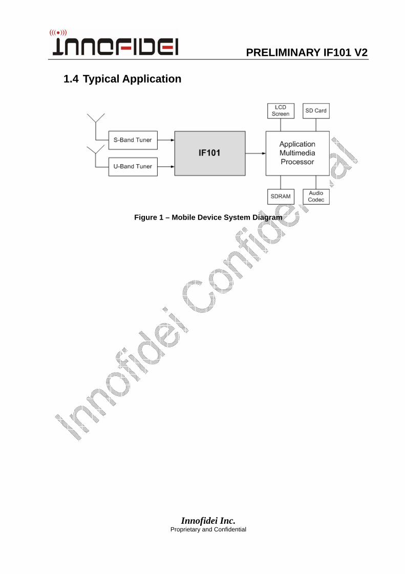
1.4 Typical Application
Figure 1 – Mobile Device System Diagram

PRELIMINARY IF101 V2
Proprietary and Confidential Innofidei Inc. 7
2 Pin Descriptions
2.1 Package/Pinout Diagrams
Figure 2 – Package Diagram for LFBGA-169

PRELIMINARY IF101 V2
Proprietary and Confidential Innofidei Inc. 8
2.2 LFBGA-169 Pin Assignment (PAD View)
PRELIMINARY IF101 V2
9 Innofidei Inc. Proprietary and Confidential
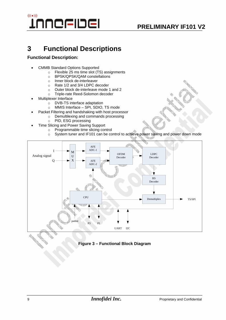
3 Functional Descriptions Functional Description: • CMMB Standard Options Supported
o Flexible 25 ms time slot (TS) assignments o BPSK/QPSK/QAM constellations o Inner block de-interleaver o Rate 1/2 and 3/4 LDPC decoder o Outer block de-interleave mode 1 and 2 o Triple-rate Reed-Solomon decoder
• Multiplexer Interface o DVB-TS interface adaptation o MMIS Interface – SPI, SDIO, TS mode
• Packet Filtering and handshaking with host processor o Demultilexing and commands processing o PID, ESG processing
• Time Slicing and Power Saving Support o Programmable time slicing control o System tuner and IF101 can be control to achieve power saving and power down mode
MUX
AFEADC-1
AFEADC-2
OFDMDecoder
LDPCDecoder
RSDecoder
DemultiplexCPUTS/SPI
padintP1P3
UART I2C
Q
IAnalog signal
Figure 3 – Functional Block Diagram

PRELIMINARY IF101 V2
Proprietary and Confidential Innofidei Inc. 10
3.1 Reset and Power-on latch
Pin name Function
PAD_TESTADC 0-> use internal ADC, 1-> use external ADC
PAD_TESTPIN 0-> enable 8051, 1 -> disable 8051
PAD_DIO13 0-> use external ADC, 1-> use internal ADC
PAD_MMIS_D7 Clock select, 1 -> use pllclk, 0 -> use refclk
PAD_MMIS_D6 Select ADC clock frequency
{PAD_MMIS_D5,
PAD_MMIS_D4}
Select GBUS clock frequency
00 -> gclk freq = 60MHz
01 -> gclk freq = 30MHz
10 -> gclk freq = 20MHz
11 -> gclk freq = 15MHz
PAD_PUP Select reference clock frequency
0 -> refclk 30Mhz
1 -> refclk 20Mhz
{ PAD_PUP ,PAD_PDN} Select TS clock frequency
00 -> 20MHz
01 -> 15MHz
10 -> 10MHz
11 -> 7.5MHz
{PAD_PDN,
PAD_LAT2,
PAD_UATXD}
The lower 3 bits of I2C slave address, which is latched up after power on.
3.2 I2C Interface (Slave Mode)
The I2C-bus supports any IC fabrication process (NMOS, CMOS, bipolar). Two wires, serial data
(SDA) and serial clock (SCL), carry information between the devices connected to the bus. Each device is recognized by a unique address (whether it’s a microcontroller, LCD driver, memory or keyboard interface) and can operate as either a transmitter or receiver, depending on the function of the device. Obviously an LCD driver is only a receiver, whereas a memory can both receive and transmit data.. A master is the device which initiates a data transfer on the bus and generates the clock signals to permit that transfer. At that time, any device addressed is considered a slave.
This version is for demodulator only chip, so the I2C master mode is not supported.

PRELIMINARY IF101 V2
Proprietary and Confidential Innofidei Inc. 11
SDA is a bi-directional line and SCL is input only line, connected to a positive supply voltage via a current-source or pull-up resistor (see Fig.3). When the bus is free, both lines are HIGH. The output stages of devices connected to the bus must have an open-drain or open-collector to perform the wired-AND function. Data on the I2C-bus can be transferred at rates of up to 100 Kbit/s in the Standard-mode, up to 400 Kbit/s in the Fast-mode, or up to
Figure 4 – Data Transfer on the I2C-bus
Data changed on the SDA line must only occur when the SCL clock is LOW. SDA transitions while the clock is HIGH are used to identify START or STOP condition.
START is identified by a HIGH to LOW transition of the data bus signal SDA while the clock signal SCL is HIGH. A START condition must precede any command for data transfer.
STOP is identified by a LOW to HIGH transition of the data bus signal SDA while the clock signal SCL is HIGH. A STOP condition terminates communications between the I2C slave and the bus master.
The first byte of data transferred by the master immediately after the START signal is the slave address. This is a seven-bit address followed by an r/w bit, which signals the data transfer direction.
Only when the address transmitted by the master matches the slave address will the I2C slave respond by pulling the SDA LOW at the 9th SCL clock cycle to return an acknowledged bit.
Every byte that is put on the SDA line must but 8-bit long. Data is transferred with the most significant bit (MSB) first.
Each byte should be followed by an acknowledged bit, which is used to indicate a successful data transfer. During the 9th clock pulse, the receiver pulls the SDA line low to acknowledge the receipt of 8 bits of data.
In this design, the I2C interface is used to configure the internal registers. So each transfer is composed of slave address, register address and register data.
START Slave addr r/w ACK Reg addr ACK Reg data ACK STOP
The higher 4 bits of the I2C slave address is 4’h2 and the lower 3 bits is determined by power-on strapping of three pins named PAD_PDN, PAD_LAT2 and PAD_UATXD. So the 7-bit slave address is {4’h2, PAD_PDN, PAD_LAT2, PAD_UATXD}, See power-on strapping section. The

PRELIMINARY IF101 V2
Proprietary and Confidential Innofidei Inc. 12
value of the lower 3 bits of the address is latched up after power on and will not vary with the state of those three pads.
The register address is 10-bit and the higher 2 bit of the address identifies the register group. To select which group of registers to configure, the user should transfer address 8’hff after the salve address in the first transmission and the lower 2 bit of the data following the address 8’hff is used as the higher 2 bit of the register address.
A complete register write operation includes:
START + Slave address(7-bit) + W(1’b0) + ACK(sent by slave) + Register address (8-bit) + ACK (sent by slave) + Register data (8-bit) + ACK (sent by slave) + STOP.
A complete register read operation includes:
START + Slave address(7-bit) + W(1’b0) + ACK(sent by slave) + Register address (8-bit) + ACK(sent by slave) + STOP + START + Slave address(7-bit) + R(1’b1) + ACK(sent by slave) +
Register data (8-bit) + ACK (sent by master) + STOP.
3.3 UART Interface
The Universal Asynchronous Receiver/Transmitter (UART) controller is the key component of the serial communications subsystem of a computer. The UART takes bytes of data and transmits the individual bits in a sequential fashion. At the destination, a second UART re-assembles the bits into complete bytes.
In IF101, only 115200 BPS is supported and the internal circuitry needs to detect the current gclk setting to adjust the internal counter to accept incoming RXD at 115200 BPS and to generate a that speed at TXD output. generate a proper TXD output at that speed.
In the definition of this design the register address and data should be preceded by two 8-bit headers and one 8-bit command and two 8-bit zero data are inserted between them.
Similar with the I2C interface, to select which group of registers to configure, the user should transfer address 8’hff after the write command in the first transmission and the lower 2 bit of the data following the address 8’hff is used as the higher 2 bit of the register address.
A complete register write operation includes:
Header 1(8’h9F) + Header 2(8’h8F) + Write command (8’h02) + 8’h00 Register address (8-bit) + 8’h00 + Register data (8-bit)
A complete register read operation includes:
Header 1(8’h9F) + Header 2(8’h8F)+ Read command (8’h01) + 8’h00 Register address (8-bit) + 8’h00 + Register data (8-bit, UART_TXD sent by slave)
Note: a) The baut rate of UART must be 11520. b) UART transmits and receives bit from LSB to MSB.

PRELIMINARY IF101 V2
Proprietary and Confidential Innofidei Inc. 13
Figure 6 UART write operation
Figure 7 UART read operation
3.4 SPI Interface
SPI is used in 1bit, 2bit, 4bit of data serial interface.
Figure 8 - SPI Mode0 Timing
PRELIMINARY IF101 V2
Proprietary and Confidential Innofidei Inc. 14
MMIS_CLK
MMIS_TXD
MMIS_RXD
MMIS_CSN
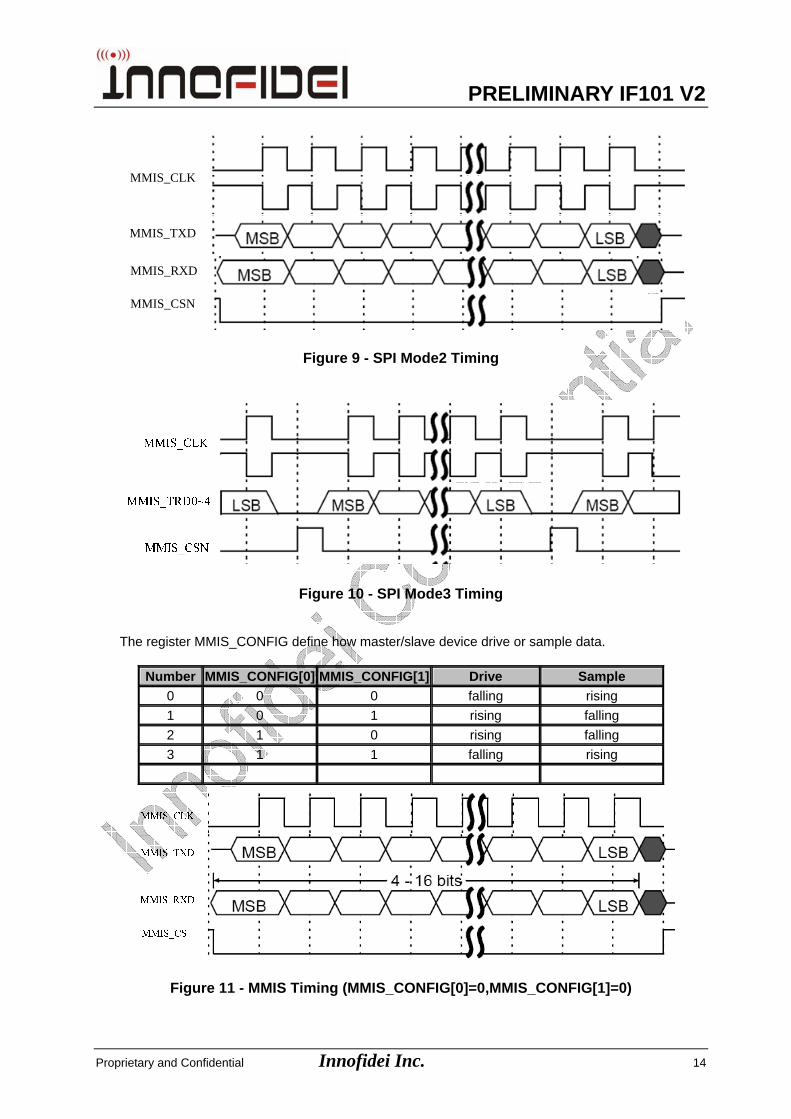
Figure 9 - SPI Mode2 Timing
Figure 10 - SPI Mode3 Timing
The register MMIS_CONFIG define how master/slave device drive or sample data.
Number MMIS_CONFIG[0] MMIS_CONFIG[1] Drive Sample 0 0 0 falling rising 1 0 1 rising falling 2 1 0 rising falling 3 1 1 falling rising
Figure 11 - MMIS Timing (MMIS_CONFIG[0]=0,MMIS_CONFIG[1]=0)

PRELIMINARY IF101 V2
Proprietary and Confidential Innofidei Inc. 15
Figure 12 - MMIS Timing (MMIS_CONFIG[0]=1,MMIS_CONFIG[1]=0)
8 bit
MMIS_CLK
MMIS_TXD
MMIS_RXD
MMIS_CS
Figure 13 - MMIS Timing (MMIS_CONFIG[0]=0,MMIS_CONFIG[1]=1)
Figure 14 - MMIS Timing (MMIS_CONFIG[0]=1,MMIS_CONFIG[1]=1)
note: The more information reference MMIS_CONFIG register.
PRELIMINARY IF101 V2
Proprietary and Confidential Innofidei Inc. 16
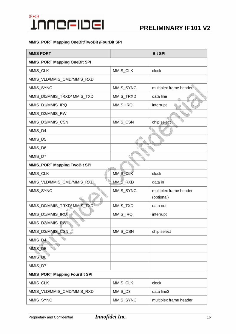
MMIS_PORT Mapping OneBit/TwoBit /FourBit SPI
MMIS PORT Bit SPI
MMIS_PORT Mapping OneBit SPI
MMIS_CLK MMIS_CLK clock
MMIS_VLD/MMIS_CMD/MMIS_RXD
MMIS_SYNC MMIS_SYNC multiplex frame header
MMIS_D0/MMIS_TRXD/ MMIS_TXD MMIS_TRXD data line
MMIS_D1/MMIS_IRQ MMIS_IRQ interrupt
MMIS_D2/MMIS_RW
MMIS_D3/MMIS_CSN MMIS_CSN chip select
MMIS_D4
MMIS_D5
MMIS_D6
MMIS_D7
MMIS_PORT Mapping TwoBit SPI
MMIS_CLK MMIS_CLK clock
MMIS_VLD/MMIS_CMD/MMIS_RXD MMIS_RXD data in
MMIS_SYNC MMIS_SYNC multiplex frame header (optional)
MMIS_D0/MMIS_TRXD/ MMIS_TXD MMIS_TXD data out
MMIS_D1/MMIS_IRQ MMIS_IRQ interrupt
MMIS_D2/MMIS_RW
MMIS_D3/MMIS_CSN MMIS_CSN chip select
MMIS_D4
MMIS_D5
MMIS_D6
MMIS_D7
MMIS_PORT Mapping FourBit SPI
MMIS_CLK MMIS_CLK clock
MMIS_VLD/MMIS_CMD/MMIS_RXD MMIS_D3 data line3
MMIS_SYNC MMIS_SYNC multiplex frame header

PRELIMINARY IF101 V2
Proprietary and Confidential Innofidei Inc. 17
(optional)
MMIS_D0/MMIS_TRXD/ MMIS_TXD MMIS_D0 data line0
MMIS_D1/MMIS_IRQ MMIS_D1 data line1
MMIS_D2/MMIS_RW MMIS_D2 data line2
MMIS_D3/MMIS_CSN MMIS_CSN spi cs
MMIS_D4
MMIS_D5
MMIS_D6
MMIS_D7
The Protocol of MMIS Interface:
Figure 15 - MMIS Protocol

PRELIMINARY IF101 V2
Proprietary and Confidential Innofidei Inc. 18
4 On-chip Microcontroller The IF101 possesses an 8-bit on-chip microcontroller as central processing unit. It provides following key features:
Compatible with standard 8051 instruction set; High speed architecture; 24K byte on-chip instruction memory; 7 interrupt sources with 4 priority levels; Bi-directional 8-bit data ports; Dual data pointers; Two 16-bit timer/counters; Enhanced memory interface with 16-bit address; Hardware watchdog timer; Six speed ranges:
- 3.75Mhz - 7.5Mhz - 15Mhz - 20Mhz; - 30Mhz; - 60Mhz

PRELIMINARY IF101 V2
Proprietary and Confidential Innofidei Inc. 19
5 Application Circuit Diagram
Figure 16 - IF101 Schematics
PRELIMINARY IF101 V2
Proprietary and Confidential Innofidei Inc. 20
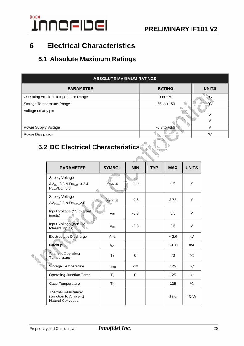
6 Electrical Characteristics
6.1 Absolute Maximum Ratings
ABSOLUTE MAXIMUM RATINGS
PARAMETER RATING UNITS
Operating Ambient Temperature Range 0 to +70 ºC
Storage Temperature Range -55 to +150 ºC
Voltage on any pin
V V
Power Supply Voltage -0.3 to +3.6 V
Power Dissipation W
6.2 DC Electrical Characteristics
PARAMETER SYMBOL MIN TYP MAX UNITS
Supply Voltage
AVDD_3.3 & DVDD_3.3 & PLLVDD_3.3
VVDD_33 -0.3 3.6 V
Supply Voltage
AVDD_2.5 & DVDD_2.5 VVDD_25 -0.3 2.75 V
Input Voltage (5V tolerant inputs) VIN -0.3 5.5 V
Input Voltage (non 5V tolerant inputs) VIN -0.3 3.6 V
Electrostatic Discharge VESD +-2.0 kV
Latchup ILA +-100 mA
Ambient Operating Temperature TA 0 70 °C
Storage Temperature TSTG -40 125 °C
Operating Junction Temp. TJ 0 125 °C
Case Temperature TC 125 °C
Thermal Resistance: (Junction to Ambient) Natural Convection
18.0 °C/W

PRELIMINARY IF101 V2
Proprietary and Confidential Innofidei Inc. 21
7 Mechanical Specifications IF101 device is supplied in 128-pin TFQFP, 14 x 14 x 1.0mm or 169-pin LFBGA, 11 x 11 x 1.4mm package. Dimensions are presented below.
Figure 175 – Package Dimension for TQFP-128

PRELIMINARY IF101 V2
Proprietary and Confidential Innofidei Inc. 22
Figure 18 - Package Dimension for LFBGA-169

PRELIMINARY IF101 V2
Proprietary and Confidential Innofidei Inc. 23
8 Register Description
8.1 Register List
Address Name Direction Function
0x003 IQ_SWITCH R/W IQ Switch 0x050 LG0_MASK1 R/W 0x051 LG0_MASK2 R/W 0x052 LG0_MASK3 R/W 0x053 LG0_MASK4 R/W 0x054 LG0_MASK5 R/W
Logical Channel 0 TS selection
0x055 LG1_MASK1 R/W 0x056 LG1_MASK2 R/W 0x057 LG1_MASK3 R/W 0x058 LG1_MASK4 R/W 0x059 LG1_MASK5 R/W
Logical Channel 1 TS selection
0x0BC SYS_STATUS R System Status 0x0BD CURR_FREQ R Current Frequency (Channel Number) 0x0BE SIG_STRENGTH R Signal Strength 0x0BF ERRRATE R Error Rate 0x0C6 VERSION_ID_YEAR R Chip Version Info (Year) 0x0C7 VERSION_ID_MONTH R Chip Version Info (Month) 0x0C8 VERSION_ID_MAIN R Chip Version Info (Main) 0x0C9 VERSION_ID_SUB R Chip Version Info (Sub) 0x0CC SYNC_STATE R SYNC State info 0x200 MODEL_SEL R/W MMIS Transfer Mode 0x201 MMIS_CONFIG R/W MMIS Transfer Configuration 0x230 LDPC_ERR_COUNTER0 R 0x231 LDPC_ERR_COUNTER1 R 0x232 LDPC_ERR_COUNTER2 R 0x233 LDPC_ERR_COUNTER3 R 0x238 LDPC_TTL_NUM0 R 0x239 LDPC_TTL_NUM1 R 0x23a LDPC_TTL_NUM2 R 0x23b LDPC_TTL_NUM3 R 0x281 CH_INFO R/W Logical Channel Selection 0x282 LG0_FETCH_MODE R/W Logical Channel 0 Fetch Mode 0x283 LG1_FETCH_MODE R/W Logical Channel 1 Fetch Mode 0x298 I2C_APData R/W 0x299 I2C_APStatus R/W 0x29a I2C_ClientData R/W 0x29b I2C_ClientStatus R/W
AP communication Registers. For more detail, please refer the “AP command spec”

PRELIMINARY IF101 V2
Proprietary and Confidential Innofidei Inc. 24
8.2 Register Function Description
8.2.1 Register – IQ_SWITCH (0x03) 0x00: IQ Normal 0x03: IQ Reversed Other Values: Illegal
8.2.2 Register – LG0_MASK1~LG0_MASK5 The register array is used to select the TS of logical channel 0 (LG0). Write “1” to enable the accordingly TS. Only the continuous TS can be put into one logical channel. For QPSK data, one logical channel can buffer 4 TS data.
LG0_MASK1: Bit0~Bit7 => TS0~TS7 LG0_MASK2: Bit0~Bit7 => TS8~TS15 LG0_MASK3: Bit0~Bit7 => TS16~TS23 LG0_MASK4: Bit0~Bit7 => TS24~TS31 LG0_MASK5: Bit0~Bit7 => TS32~TS39 NOTE: In IF101V2 chip, the new power management algorithm has been implemented. To get the best power saving performance, we don’t encourage the customer to switch the TS by writing these registers. It may cause some unpredicted result. To switch TS, please use the standard API interface.
8.2.3 Register – LG1_MASK1~LG1_MASK5 The register array is used to select the TS of logical channel 1 (LG0). Write “1” to enable the accordingly TS. Only the continuous TS can be put into one logical channel. For QPSK data, one logical channel can buffer 4 TS data.
LG1_MASK1: Bit0~Bit7 => TS0~TS7 LG1_MASK2: Bit0~Bit7 => TS8~TS15 LG1_MASK3: Bit0~Bit7 => TS16~TS23 LG1_MASK4: Bit0~Bit7 => TS24~TS31 LG1_MASK5: Bit0~Bit7 => TS32~TS39 NOTE: In IF101V2 chip, the new power management algorithm has been implemented. To get the best power saving performance, we don’t encourage the customer to switch the TS by writing these registers. It may cause some unpredicted result. To switch TS, please use the standard API interface.

PRELIMINARY IF101 V2
Proprietary and Confidential Innofidei Inc. 25
8.2.4 Register – SYS_STATUS (0x0BC) Read only registers, System Status Bit7: PWRON 0: Chip is in power saving state 1: Chip is in normal working mode Bit0: CPTYPE 0: Short CP mode, 40TS 1: Long CP mode, 36TS
8.2.5 Register – CURR_FREQ (0x0BD) Current receiving frequency, (Channel number) Please refer the following table for the frequency of each channel. This is a read only register. AP can’t write this register to switch the receiving frequency. To change the receiving frequency, please use the “INNO_SetTunerFrequency” API. CH Freq CH Freq CH Freq CH Freq 18 514 MHZ 35 690 MHZ 52 826 MHZ 19 522 MHZ 36 698 MHZ 53 834 MHZ 20 530 MHZ 37 706 MHZ 54 842 MHZ 21 538 MHZ 38 714 MHZ 55 850 MHZ 22 546 MHZ 39 722 MHZ 56 858 MHZ 23 554 MHZ 40 730 MHZ 57 866 MHZ 24 562 MHZ 41 738 MHZ 58 874 MHZ 25 610 MHZ 42 746 MHZ 59 26 618 MHZ 43 754 MHZ 60 882 MHZ 27 626 MHZ 44 762 MHZ 61 890 MHz 28 634 MHZ 45 770 MHZ 62 898 MHZ 29 642 MHZ 46 778 MHZ 63 906 MHZ 13 474 MHZ 30 650 MHZ 47 786 MHZ 64 914 MHZ 14 482 MHZ 31 658 MHZ 48 794 MHZ 65 922 MHZ 15 491 MHZ 32 666 MHZ 49 802 MHZ 66 930 MHZ 16 498 MHZ 33 674 MHZ 50 810 MHZ 67 938 MHZ 17 506 MHZ 34 682 MHZ 51 818 MHZ 68 946 MHZ 101 102 103
8.2.6 Register – SIG_STRENGTH (0x0BE)
Receiving signal strength (dB) 0x00: 0dB 0x01: -1dB …… 0x63: -99dB 0x64-0xff: <-99dB

PRELIMINARY IF101 V2
Proprietary and Confidential Innofidei Inc. 26
8.2.7 Register – ERRRATE (0x0BF)
LDPC error rate. 0x00: no LDPC error 0x01: 1% LDPC error 0x02: 2% LDPC error …… 0x64: 100% LDPC error
8.2.8 Register – VERSION_ID_xxxx (0x0C6-0x0C9)
Read only registers to identity the chip version.
8.2.9 Register – SYNC_STATE (0x0CC) Chip Sync State 0x00: No signal 0x01-0x07: SYNC is on processing 0x08: SYNC OK 0x09: SYNC fail
8.2.10 Register – MODEL_SEL (0x200) MMIS interface transfer model select. Bit3..0 : 0000: Transfer mode 1 0001: Reserved 0010: Transfer mode 2 0100: Transfer mode 3 0101: Reserved 1000: Transfer mode 4 Other: Illegal
8.2.11 Register –MMIS_CONFIG (0x201) MMIS mode configuration register Bit0: SCLK Pol Bit1: SCLK Pha Bit2: LSB Bit4..Bit3: Data transfer mode 00: 8 bits mode 01: 16 bits mode 10: 32 bits mode 11: Burst mode
8.2.12 Register – LDPC_ERR_COUNTERx and LDPC_TTL_NUMx
LDPC_ERR_COUNTER0 ~ LDPC_ERR_COUNTER0 : LDPC error counter 32 bits. LDPC_TTL_COUNTER0 ~ LDPC_TTL_COUNTER0 : LDPC total block counter 32 bits.
LDPC_TTL_COUNTERx register is counting the total decoded blocks. For 4 TS QPSK data, there are

PRELIMINARY IF101 V2
Proprietary and Confidential Innofidei Inc. 27
total 120 LDPC blocks decoded per second.
LDPC_ERR_COUNTERx register is counting the error LDPC blocks. 8.2.13 Register – CH_INFO
Bit0: Logical channel 0 select. “1” to enable. Bit1: Logical channel 1 select. “1” to enable. Bit2: TS0 select. “1” to enable. NOTE: This register is updated by firmware. Don’t try to modify it.
8.2.14 Register – LG0_FETCH_MODE
Bit2..Bit0: LDPC and Outer mode 000: 72x240 1/2 LDPC 001: 108x240 3/4 LDPC 010: 144x240 1/2 LDPC 011: 216x240 3/4 LDPC 100: 288x240 1/2 LDPC Bit4..3: RS mode 00: 240, 176 01: 240, 192 10: 240, 224 11: 240, 240 NOTE: This register is updated by firmware. Don’t try to modify it.
8.2.15 Register – LG1_FETCH_MODE
Bit2..Bit0: LDPC and Outer mode 000: 72x240 1/2 LDPC 001: 108x240 3/4 LDPC 010: 144x240 1/2 LDPC 011: 216x240 3/4 LDPC 100: 288x240 1/2 LDPC Bit4..3: RS mode 00: 240, 176 01: 240, 192 10: 240, 224 11: 240, 240 NOTE: This register is updated by firmware. Don’t try to modify it.
8.2.16 Register – AP communication registers
I2C_APData I2C_APStatus I2C_ClientData
I2C_ClientStatus For more detail of the AP communication registers, please refer the

PRELIMINARY IF101 V2
Proprietary and Confidential Innofidei Inc. 28
“IF101_Driver_Development_Guide”.
8.3 MMIS Command List
MMIS Command List Name Value Description
READ_MODE_SEL 0x01 Read mode register
READ_MMIS_CONFIG 0x02 Read MMIS data transfer control register
READ_INT0_ENABLE 0x04 Read interrupt mask register 0
READ_INT1_ENABLE 0x05 Read interrupt mask register 1
READ_INT2_ENABLE 0x06 Read interrupt mask register 2
WRITE_INT0_ENABLE 0x07 Write interrupt mask register 0
WRITE_INT1_ENABLE 0x08 Write interrupt mask register 1
WRITE_INT2_ENABLE 0x09 Write interrupt mask register 2
READ_INT0_STATUS 0x0a Read interrupt status 0
READ_INT1_STATUS 0x0b Read interrupt status 1
READ_INT2_STATUS 0x0c Read interrupt status 2
READ_DEMOD_STATUS 0x03 Read demodulator status
READ_LG0_FILTER_PID_L 0x0d Read LG0 filter (Low)
WRITE_LG0_FILTER_PID_L 0x0e Write LG0 filter (Low)
READ_LG0_FILTER_PID_H 0x0f Read LG0 filter (High)
WRITE_LG0_FILTER_PID_H 0x10 Write LG0 filter (High)
READ_LG1_FILTER_PID_L 0x11 Read LG1 filter (Low)
WRITE_LG1_FILTER_PID_L 0x12 Write LG1 filter (Low)
READ_LG1_FILTER_PID_H 0x13 Read LG1 filter (High)
WRITE_LG1_FILTER_PID_H 0x14 Write LG1 filter (High)
READ_LG0_LEN_LOW 0x15 Read LG0 length (Low)
READ_LG0_LEN_MID 0x16 Read LG0 length (Mid)
READ_LG0_LEN_HIGH 0x17 Read LG0 length (High)
READ_LG1_LEN_LOW 0x18 Read LG1 length (Low)
READ_LG1_LEN_MID 0x19 Read LG1 length (Mid)

PRELIMINARY IF101 V2
Proprietary and Confidential Innofidei Inc. 29
READ_LG1_LEN_HIGH 0x1a Read LG1 length (High)
FETCH_LG0_DATA 0x99 Fetch LG0 Data
FETCH_LG1_DATA 0x9b Fetch LG1 Data
READ_TS0_LEN_LOW 0x1b Read TS0 Length (Low)
READ_TS0_LEN_MID 0x1c Read TS0 Length (Mid)
READ_TS0_LEN_HIGH 0x1d Read TS0 Length (High)
FETCH_TS0_DATA 0x9d Fetch TS0 Data
PREPARE TS0 DATA 0x1e Prepare TS0 data
PREPARE TS1 DATA 0x1f Prepare TS1 data
TX_ABORT/SDIO-Abort/ 0x40 Master device terminate the transfer
8.4 SDIO Command List
SDIO Command List Name Value Description
PREPARE TS0 DATA 0x00 Inform IF101 to prepare TS0 data
PREPARE TS1 DATA 0x01 Inform IF101 to prepare TS1 data
FETCH TS0 DATA 0x02 Transfer TS0 Data to AP
FETCH LG0 DATA 0x03 Transfer TS0 Data to AP
FETCH LG1 DATA 0x04 Transfer TS0 Data to AP
ERASE PAGE 0xe0 Erase EEPROM
ABORT 0xf2 AP send Abort

PRELIMINARY IF101 V2
Proprietary and Confidential Innofidei Inc. 30
9 Application Notes
9.1 Demodulator Driver Programming
Please refer the separate document “IF101_Driver_Development_Guide” for the detail of driver programming.
9.2 DeMux Programming
Please refer the separate document “Innofidei Demodulator Embeded Device SDK Programmer Manual” for the detail of DeMux programming. Information provided by Innofidei Inc. in this datasheet is believed to be accurate and reliable; however, Innofidei Inc. assumes no responsibility for its use or any infringement of patents. Innofidei Inc. reserves the right to make changes to their products or specifications, or to discontinue any product, without notice, at any time. Innofidei Inc. recommends customers obtain the latest version of information before placing orders.