
IEEE TRANSACTIONS ON POWER ELECTRONICS,...
11
IEEE TRANSACTIONS ON POWER ELECTRONICS, VOL. 32, NO. 10, OCTOBER 2017 7591 Single-Stage Three-Phase Current-Source Photovoltaic Grid-Connected Inverter High Voltage Transmission Ratio Daolian Chen, Senior Member, IEEE, Jiahui Jiang, Yanhui Qiu, Jie Zhang, and Fusong Huang Abstract—This paper proposes a circuit topology of a single- stage three-phase current-source photovoltaic (PV) grid-connected inverter with high voltage transmission ratio (VTR). Also, an im- proved zone sinusoidal pulsewidth modulation (SPWM) control strategy and an active-clamped subcircuit that can suppress the energy storage switch’s turn-off voltage spike are introduced. The circuit topology, control strategy, steady principle characteristics, and high-frequency switching process are analyzed profoundly, as well as the VTR’s expression and design criterion of the center- tapped energy storage inductor. The improved zone SPWM con- trol strategy consists of two control loops, namely, the outer loop of input dc voltage of PV cells with the maximum power point tracking and the inner loop of the energy storage inductor current. The experimental results of a 3-kW 96VDC/380V50Hz3ϕAC pro- totype have shown that this kind of a three-phase inverter has the excellent performances such as single-stage power conversion, high VTR and power density, and high conversion efficiency. Nonethe- less, it has small energy storage inductor and output CL filter, low output current total harmonic distortion, and flexible voltage con- figuration of the PV cells. This study provides an effective design method for single-stage three-phase inverting with high VTR. Index Terms—Current source, high voltage transmission ra- tio (VTR), photovoltaic (PV) grid-connected inverter, three-phase, zone Sinusoidal Pulse width modulation (SPWM) control strategy. I. INTRODUCTION A T PRESENT, the photovoltaic (PV) grid-connected power generation systems commonly adopt the voltage source circuit, which requires the value of dc voltage higher than the peak value of ac voltage. Therefore, an obvious defect arises. When the output capability of the PV cells weakens, i.e., in rainy day or at night, the operation of the whole system stops, along with the decrease of its utilization rate [1]–[6]. PV cells operate as current source, therefore, the current- source inverter (CSI) is more suitable for the PV power Manuscript received February 28, 2016; revised June 18, 2016 and September 19, 2016; accepted October 24, 2016. Date of publication November 2, 2016; date of current version May 9, 2017. This work was supported by the Key Project of Natural Science Foundation of China, under Grant 51537001. Recommended for publication by Associate Editor Prof. M. Vitelli. The authors are with the Fujian Key Laboratory of New Energy Generation and Power Conversion, Fuzhou University, Fuzhou 350116, China (e-mail: [email protected]; [email protected]; qyh522@ sina.com; [email protected]; [email protected]). Color versions of one or more of the figures in this paper are available online at http://ieeexplore.ieee.org. Digital Object Identifier 10.1109/TPEL.2016.2622722 generation system. Compared with the voltage-source inverter, the CSI has the following characteristics [7]–[17]: 1) boosting feature, the input dc current can be manipu- lated by controlling the magnetizing time of the energy storage inductor, so as to realize the whole process of light utilization from weak to strong; 2) direct control of the output current, thus it is more conve- nient and reliable to realize maximum power point track- ing (MPPT), yet the voltage source inverter can cause a dc bus crash and the reliability is accordingly reduced; 3) inductor as the energy storage component, thus the system operation time is longer than that of the voltage source inverter, which uses the electrolytic capacitor as energy storage component; 4) timely protection for overcurrent, which provides a high reliability. The single-stage three-phase current-source PWM inverter with low voltage transmission ratio (VTR) proposed in [12]– [17] has the advantages of single-stage power conversion, boost- ing feature, and timely overcurrent protection, but there still exists the flaws. The VTR is not high enough, and the output waveform quality and conversion efficiency will be seriously affected when the input voltage is too low or the input volt- age variation range is too wide. For example, a 120–200VDC/ 380V50Hz3ϕAC inverter can be achieved, but when the input voltage is lower than 120 V, the duty ratio D is close to the limit value, 1–D is too small, thus the adjusting range of D is limited. This would cause some problems such as poor dynamic char- acteristics, decrease of the VTR caused by the circuit parasitic parameters, large energy storage inductor current and circuit loss, low conversion efficiency, and worse output waveform. Therefore, it is difficult to invert for low voltage of the PV cells. In order to overcome the limitations of the traditional volt- age source PWM inverter [1]–[6] and single-stage three-phase current-source PWM inverter with low VTR [12]–[17], this pa- per proposes a single-stage three-phase CSI with high VTR, as well as the circuit topology and an improved zone sinusoidal pulsewidth modulation (SPWM) control strategy with two con- trol loops. The loops are consisted of the outer loop of input dc voltage with MPPT and the inner loop of the storage inductor current. Besides, an active-clamped subcircuit that can suppress the energy storage switch’s turn-off voltage spike is discussed in this paper, with important conclusions obtained. 0885-8993 © 2016 IEEE. Personal use is permitted, but republication/redistribution requires IEEE permission. See http://www.ieee.org/publications standards/publications/rights/index.html for more information.
-
Upload
phungkhanh -
Category
Documents
-
view
234 -
download
3
Transcript of IEEE TRANSACTIONS ON POWER ELECTRONICS,...
IEEE TRANSACTIONS ON POWER ELECTRONICS, VOL. 32, NO. 10, OCTOBER 2017 7591
Single-Stage Three-Phase Current-SourcePhotovoltaic Grid-Connected Inverter
High Voltage Transmission RatioDaolian Chen, Senior Member, IEEE, Jiahui Jiang, Yanhui Qiu, Jie Zhang, and Fusong Huang
Abstract—This paper proposes a circuit topology of a single-stage three-phase current-source photovoltaic (PV) grid-connectedinverter with high voltage transmission ratio (VTR). Also, an im-proved zone sinusoidal pulsewidth modulation (SPWM) controlstrategy and an active-clamped subcircuit that can suppress theenergy storage switch’s turn-off voltage spike are introduced. Thecircuit topology, control strategy, steady principle characteristics,and high-frequency switching process are analyzed profoundly, aswell as the VTR’s expression and design criterion of the center-tapped energy storage inductor. The improved zone SPWM con-trol strategy consists of two control loops, namely, the outer loopof input dc voltage of PV cells with the maximum power pointtracking and the inner loop of the energy storage inductor current.The experimental results of a 3-kW 96VDC/380V50Hz3ϕAC pro-totype have shown that this kind of a three-phase inverter has theexcellent performances such as single-stage power conversion, highVTR and power density, and high conversion efficiency. Nonethe-less, it has small energy storage inductor and output CL filter, lowoutput current total harmonic distortion, and flexible voltage con-figuration of the PV cells. This study provides an effective designmethod for single-stage three-phase inverting with high VTR.
Index Terms—Current source, high voltage transmission ra-tio (VTR), photovoltaic (PV) grid-connected inverter, three-phase,zone Sinusoidal Pulse width modulation (SPWM) control strategy.
I. INTRODUCTION
A T PRESENT, the photovoltaic (PV) grid-connected powergeneration systems commonly adopt the voltage source
circuit, which requires the value of dc voltage higher than thepeak value of ac voltage. Therefore, an obvious defect arises.When the output capability of the PV cells weakens, i.e., in rainyday or at night, the operation of the whole system stops, alongwith the decrease of its utilization rate [1]–[6].
PV cells operate as current source, therefore, the current-source inverter (CSI) is more suitable for the PV power
Manuscript received February 28, 2016; revised June 18, 2016 and September19, 2016; accepted October 24, 2016. Date of publication November 2, 2016;date of current version May 9, 2017. This work was supported by the Key Projectof Natural Science Foundation of China, under Grant 51537001. Recommendedfor publication by Associate Editor Prof. M. Vitelli.
The authors are with the Fujian Key Laboratory of New EnergyGeneration and Power Conversion, Fuzhou University, Fuzhou 350116,China (e-mail: [email protected]; [email protected]; [email protected]; [email protected]; [email protected]).
Color versions of one or more of the figures in this paper are available onlineat http://ieeexplore.ieee.org.
Digital Object Identifier 10.1109/TPEL.2016.2622722
generation system. Compared with the voltage-source inverter,the CSI has the following characteristics [7]–[17]:
1) boosting feature, the input dc current can be manipu-lated by controlling the magnetizing time of the energystorage inductor, so as to realize the whole process of lightutilization from weak to strong;
2) direct control of the output current, thus it is more conve-nient and reliable to realize maximum power point track-ing (MPPT), yet the voltage source inverter can cause adc bus crash and the reliability is accordingly reduced;
3) inductor as the energy storage component, thus the systemoperation time is longer than that of the voltage sourceinverter, which uses the electrolytic capacitor as energystorage component;
4) timely protection for overcurrent, which provides a highreliability.
The single-stage three-phase current-source PWM inverterwith low voltage transmission ratio (VTR) proposed in [12]–[17] has the advantages of single-stage power conversion, boost-ing feature, and timely overcurrent protection, but there stillexists the flaws. The VTR is not high enough, and the outputwaveform quality and conversion efficiency will be seriouslyaffected when the input voltage is too low or the input volt-age variation range is too wide. For example, a 120–200VDC/380V50Hz3ϕAC inverter can be achieved, but when the inputvoltage is lower than 120 V, the duty ratio D is close to the limitvalue, 1–D is too small, thus the adjusting range of D is limited.This would cause some problems such as poor dynamic char-acteristics, decrease of the VTR caused by the circuit parasiticparameters, large energy storage inductor current and circuitloss, low conversion efficiency, and worse output waveform.Therefore, it is difficult to invert for low voltage of the PV cells.
In order to overcome the limitations of the traditional volt-age source PWM inverter [1]–[6] and single-stage three-phasecurrent-source PWM inverter with low VTR [12]–[17], this pa-per proposes a single-stage three-phase CSI with high VTR, aswell as the circuit topology and an improved zone sinusoidalpulsewidth modulation (SPWM) control strategy with two con-trol loops. The loops are consisted of the outer loop of input dcvoltage with MPPT and the inner loop of the storage inductorcurrent. Besides, an active-clamped subcircuit that can suppressthe energy storage switch’s turn-off voltage spike is discussedin this paper, with important conclusions obtained.
0885-8993 © 2016 IEEE. Personal use is permitted, but republication/redistribution requires IEEE permission.See http://www.ieee.org/publications standards/publications/rights/index.html for more information.
7592 IEEE TRANSACTIONS ON POWER ELECTRONICS, VOL. 32, NO. 10, OCTOBER 2017
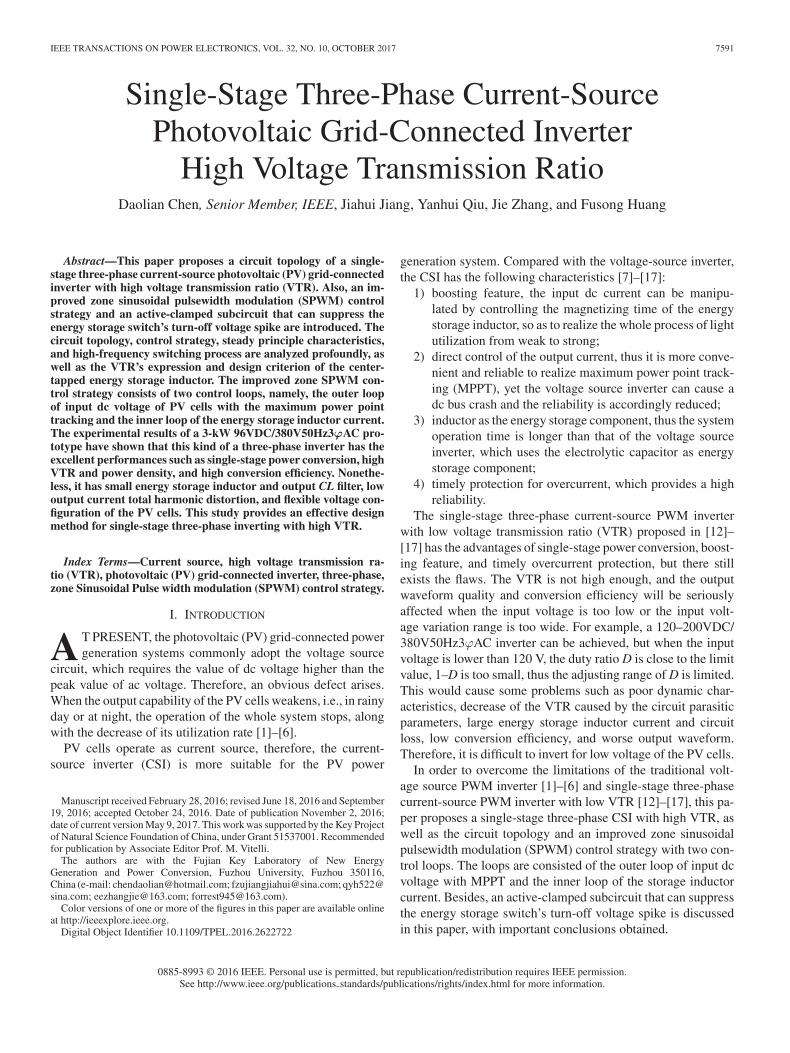
Fig. 1. Circuit topology of a single-stage three-phase current-source PV grid-connected inverter with high VTR.
II. CIRCUIT TOPOLOGY AND CONTROL STRATEGY
A. Control Strategy
The circuit topology of a single-stage three-phase current-source PV grid-connected inverter with high VTR is shown inFig. 1. The circuit topology is sequentially cascaded by the inputfilter capacitor C, the center-tapped energy storage inductor L,three-phase inverting bridge with six serial blocking diodes andan output CL filter. An energy storage switch S is connectedbetween the center tap of L and the negative end of the PV cells,the left and right turns number of L are N1 and N2 , respectively.Compared to CSI with low VTR [12]–[17], a center tap of theenergy storage inductor and an energy storage switch are addedto the proposed CSI.
An active-clamped subcircuit connected in parallel at bothends of S shown in Fig. 1 is proposed, in order to suppressthe turn-off voltage spike of S, which is caused by the leakageinductor of L1 . The active-clamped subcircuit is consisted ofactive-clamped switch Sc and a serial clamping capacitor Cc .
The VTR of the proposed CSI depends on both the energystorage duty ratio and the center tap position of L, and it providesa possibility to realize high VTR inverting.
B. Two-Loop Improved Zone SPWM Control Strategy
1) Improved Zone SPWM Control Strategy: An improvedzone SPWM control strategy is proposed in the single-stagethree-phase current-source PV grid-connected inverter with highVTR. The reference signal that has the same frequency butdifferent in phase of θ with the grid voltage is divided into six60° intervals in a line cycle by the zero crossing point, thusthere exist only two line voltages that is always ≥ √
6/2 Up
in every 60° interval, where Up is root mean square (RMS)value of the phase voltage. This control strategy can ensurethe normal operation of the CSI in any high-frequency (HF)switching period with the condition that output line voltage arenot smaller than input voltage, i.e.,
√6/2 Up ≥ UPV , and obtain
high quality of the output grid-connected current.Set the three-phase grid voltage ua , ub , and uc as
⎧⎪⎨
⎪⎩
ua =√
2Up sin (ωt + θ)
ub =√
2Up sin(ωt − 2π/3 + θ)
uc =√
2Up sin(ωt − 4π/3 + θ).
(1)
Three-phase reference signals ea , eb , and ec , which have thesame frequency but phase difference of θ with the grid voltages
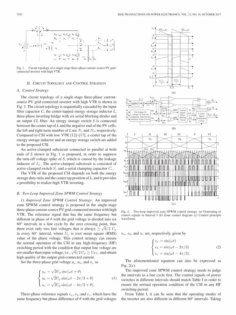
Fig. 2. Two-loop improved zone SPWM control strategy. (a) Generating ofcontrol signals in Interval I (b) Zone control diagram (c) Control principlewaveforms.
ua , ub , and uc are, respectively, given by⎧⎪⎨
⎪⎩
ea = sin(ωt)
eb = sin(ωt − 2π/3)
ec = sin(ωt − 4π/3).
(2)
The aforementioned equation can also be expressed asFig. 2(c).
The improved zone SPWM control strategy needs to judgethe intervals in a line cycle first. The control signals of powerswitches in different intervals should match Table I in order toensure the normal operation condition of the CSI in any HFswitching period.
From Table I, it can be seen that the operating modes ofthe inverter are also different in different 60° intervals. Taking
CHEN et al.: SINGLE-STAGE THREE-PHASE CURRENT-SOURCE PHOTOVOLTAIC GRID-CONNECTED INVERTER HIGH VTR 7593
TABLE ICONTROL SIGNALS OF THE POWER SWITCHES IN DIFFERENT INTERVALS
the Interval I as an example, Sb2 is ON, Sa2 , Sb1 , and Sc2are OFF, and the power switches S, Sa1 , and Sc1 are SPWMmodulated, as shown in Fig. 2(a). In Fig. 2(a), k is the samplingcoefficient of the energy storage inductor current iL , and ILavgis the average value of iL in one HF switching period TS , TS /2is the sawtooth carrier wave period. The control signals of S andSa1 are generated by comparing the modulation signal kILavgea
with the former switching period sawtooth wave uc , whereasthe control signals of S and Sc1 are generated by comparing themodulation signal kILavgec with the latter switching period uc .
2) Two-Loop Improved Zone SPWM Control Strategy: Two-loop improved zone SPWM control strategy of input dc voltagein outer loop and energy storage inductor current in inner loopis adopted in the proposed three-phase grid-connected inverter,as shown in Fig. 2(b) and (c).
The grid-connected current reference signals ea , eb , and ec
obtained by sampling the grid voltage ua , ub , and uc have phasedifference θ with the grid voltage. The energy storage induc-tor current signal iL = (iL1 + N2/N1iL2) is obtained throughsampling the energy storage inductor current iL1 and iL2 , whileiL2 converted to iL1 to guarantee the continuity of the sampledcurrent in one switching period. By detecting the output voltageUPV and output current IPV of PV cells, maximum power point(MPP) voltage is set as the reference voltage U ∗
PV of PV cellsthrough MPPT calculation. The difference value of the U ∗
PVand UPV is amplified to get signal k, the average value ILavg isobtained by sampling iL once every switching period. Throughthe output low-frequency (LF) voltage’s six intervals judgment,selection and absolute value circuit according to Table I, signalsm1 and m2 of the corresponding interval are obtained. m1 andm2 are, respectively, multiplied by kILavg to generate two mod-ulation wave signals ue1 = kILavgm1 , ue2 = kILavgm2 , thenthey are, respectively, compared with the sawtooth carrier waveuc to obtain the SPWM control signals of this interval. Signalsn1 and n2 of the power switches are obtained after the signalphase-splitting circuit because the frequency of the energy re-lease switches is half the frequency of the carrier wave, andthen, the signals of the energy storage switch S and the energyrelease switches of the three-phase inverting bridge are obtainedby the signal distribution circuit according to Table I.
III. STEADY PRINCIPLE
A. LF Mode Analysis
There are six operating intervals in a line cycle of the inverter,and each interval can be divided into three operating modes.
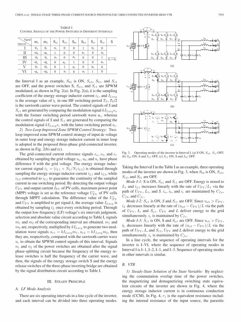
Fig. 3. Operating modes of the inverter in Interval I. (a) S ON, Sa1, Sc1 OFF,(b) Sa1 ON, S and Sc1 OFF, (c) Sc1 ON, S and Sa1 OFF.
Taking the Interval I in the Table I as an example, three operatingmodes of the inverter are shown in Fig. 3, when Sb2 is ON, Sa2 ,Sc2 , and Sb1 are OFF.
Mode I-1: S is ON, Sa1 and Sc1 are OFF. Energy is stored toL1 and iL1 increases linearly with the rate of UPV/L1 via thepath of UPV , L1 , and S. ia , ib , and ic are maintained by Cf a ,Cf b , and Cf c .
Mode I-2: Sa1 is ON, S and Sc1 are OFF. Since uab > UPV ,iL decreases linearly at the rate of (uab − UPV)/L via the pathof UPV , L, and Sa1 . UPV and L deliver energy to the gridsimultaneously. ic is maintained by Cf c .
Mode I-3: Sc1 is ON, S and Sa1 are OFF. Since ucb > UPV ,iL decreases linearly with the rate of (ucb − UPV)/L via thepath of UPV , L, and Sc1 , UPV and L deliver energy to the gridsimultaneously. ia is maintained by Cf a .
In a line cycle, the sequence of operating intervals for theinverter is I–VI, where the sequence of operating modes inInterval I is I–1, I–2, I–1, and I–3. Sequence of operating modesin other intervals is similar.
B. VTR
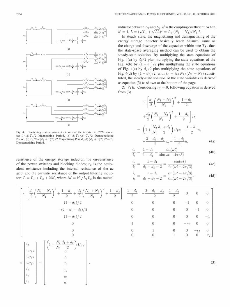
1) Steady-State Solution of the State Variable: By neglect-ing the commutation overlap time of the power switches,the magnetizing and demagnetizing switching state equiva-lent circuits of the inverter are shown in Fig. 4, where theenergy storage inductor current is in continuous conductionmode (CCM). In Fig. 4, r1 is the equivalent resistance includ-ing the internal resistance of the input source, the parasitic
7594 IEEE TRANSACTIONS ON POWER ELECTRONICS, VOL. 32, NO. 10, OCTOBER 2017
Fig. 4. Switching state equivalent circuits of the inverter in CCM mode.(a) 0∼d1 Ts /2 Magnetizing Period, (b) d1 TS /2∼Ts /2 DemagnetizingPeriod, (c) Ts /2∼(d2 + 1)Ts /2 Magnetizing Period, (d) (d2 + 1)Ts /2∼Ts
Demagnetizing Period.
resistance of the energy storage inductor, the on-resistanceof the power switches and blocking diodes; r2 is the equiv-alent resistance including the internal resistance of the acgrid, and the parasitic resistance of the output filtering induc-tor; L = L1 + L2 + 2M , where M = k′√L1L2 is the mutual
inductor between L1 and L2 , k′ is the coupling coefficient. Whenk′ = 1, L = (
√L1 +
√L2)2 = L1 [(N1 + N2)/N1 ]2 .
In steady state, the magnetizing and demagnetizing of theenergy storage inductor basically reach balance, same asthe charge and discharge of the capacitor within one TS , thusthe state-space averaging method can be used to obtain thesteady-state solution. By multiplying the state equations ofFig. 4(a) by d1/2 plus multiplying the state equations of theFig. 4(b) by (1 − d1)/2 plus multiplying the state equationsof Fig. 4(c) by d2/2 plus multiplying the state equations ofFig. 4(d) by (1 − d2)/2, with iL = iL1N1/(N1 + N2) substi-tuted, the steady-state solution of the state variables is derivedas equation (3) as shown at the bottom of the page.
2) VTR: Considering r2 = 0, following equation is derivedfrom (3)
r1
[d1
2
(N1 + N2
N1
)2
+1 − d1
2
+d2
2
(N1 + N2
N1
)2
+1 − d2
2
]
iL
=(
1 +N2
N1
d1 + d2
2
)
UPV − 1 − d1
2ua
+2 − d1 − d2
2ub − 1 − d2
2uc (4a)
iaic
=1 − d1
1 − d2=
sin(ωt)sin(ωt − 4π/3)
(4b)
iaib
=1 − d1
d1 + d2 − 2=
sin(ωt)sin(ωt − 2π/3)
(4c)
icib
=1 − d2
d1 + d2 − 2=
sin(ωt − 4π/3)sin(ωt − 2π/3)
. (4d)
⎡
⎢⎢⎢⎢⎢⎢⎢⎢⎢⎢⎢⎢⎢⎢⎢⎣
r1
[d1
2
(N1 + N2
N1
)2
+1 − d1
2+
d2
2
(N1 + N2
N1
)2
+1 − d2
2
]1 − d1
2−2 − d1 − d2
21 − d2
20 0 0
(1 − d1)/2 0 0 0 −1 0 0
−(2 − d1 − d2)/2 0 0 0 0 −1 0
(1 − d2)/2 0 0 0 0 0 −1
0 1 0 0 −r2 0 0
0 0 1 0 0 −r2 00 0 0 1 0 0 −r2
⎤
⎥⎥⎥⎥⎥⎥⎥⎥⎥⎥⎥⎥⎥⎥⎥⎦
×
⎡
⎢⎢⎢⎢⎢⎢⎢⎢⎢⎢⎢⎢⎣
iL
uC f a
uC f b
uC f c
ia
ib
ic
⎤
⎥⎥⎥⎥⎥⎥⎥⎥⎥⎥⎥⎥⎦
=
⎡
⎢⎢⎢⎢⎢⎢⎢⎢⎢⎢⎢⎢⎢⎣
(
1 +N2
N1
d1 + d2
2
)
UPV
0
0
0
ua
ub
uc
⎤
⎥⎥⎥⎥⎥⎥⎥⎥⎥⎥⎥⎥⎥⎦
. (3)
CHEN et al.: SINGLE-STAGE THREE-PHASE CURRENT-SOURCE PHOTOVOLTAIC GRID-CONNECTED INVERTER HIGH VTR 7595
Set 1 − d1 = Ksin(ωt) = Kea (K ∈ (0, 1)), so 1 − d2 =Ksin(ωt − 4π/3) = Kec , 2 − d1 − d2 =Ksin(ωt − 2π/3) =Keb . In Interval I, |sin(ωt − 2π/3)| can be expressed by theaverage value 3/π, so d1 + d2 ≈ 2 − K, (4a) can be simplifiedas
(
1 +N2
N1
2 − 3K/π
2
)
UPV = K
[
ua sin(ωt)
+ub
2sin
(
ωt − 2π
3
)
+ uc sin(
ωt − 4π
3
)]
+r1
[12
(N1 + N2
N1
)2 (
2 − 3K
π
)
+3K
2π
]
iL (5)
the input dc current IPV can be expressed as
IPV =d1iL1
2+
1 − d1
2iL +
d2iL1
2+
1 − d2
2iL
=[
1 +(
1 − 3K
2π
)N2
N1
]
iL (6)
assuming that the RMS of output phase current is Ip , the effi-ciency of the inverter is η, then
IPV = 3UpIp/ (UPVη) (7)
derived from (6) and (7)
iL = 3UpIp
/{
UPVη
[
1 +(
1 − 3K
2π
)N2
N1
]}
(8)
substituting (1) and (8) into (4a), one can obtain
Up =UPV [1 + (N2/N1) (2 − 3K/π) /2]
3√
2K4 + 3Ipr1
[(N1 +N2 )/N1 ]2 (2−3K/π )/2+3K/(2π )UP V η [1+(N2 /N1 )(1−3K/(2π ))]
. (9)
Assuming that r1 = 0, η = 100%, and the inverter in CCMmode, the ideal VTR Up/UPV is
Up
UPV=
2√
2 [1 + (N2/N1)]3K
−√
2 (N2/N1)π
(10)
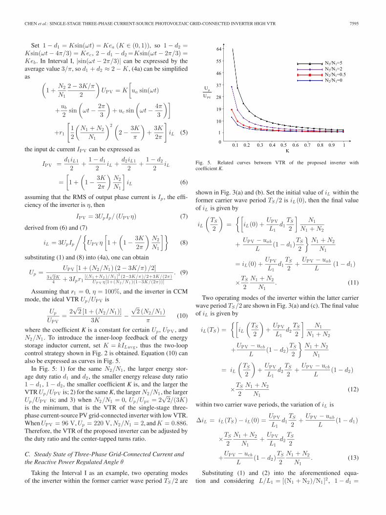
where the coefficient K is a constant for certain Up , UPV , andN2/N1 . To introduce the inner-loop feedback of the energystorage inductor current, set K = kILavg , thus the two-loopcontrol strategy shown in Fig. 2 is obtained. Equation (10) canalso be expressed as curves in Fig. 5.
In Fig. 5: 1) for the same N2/N1 , the larger energy stor-age duty ratio d1 and d2 , the smaller energy release duty ratio1 − d1 , 1 − d2 , the smaller coefficient K is, and the larger theVTR Up/UPV is; 2) for the same K, the larger N2/N1 , the largerUp/UPV is; and 3) when N2/N1 = 0, Up/Upv = 2
√2/(3K)
is the minimum, that is the VTR of the single-stage three-phase current-source PV grid-connected inverter with low VTR.When UPV = 96 V, Up = 220 V, N2/N1 = 2, and K = 0.886.Therefore, the VTR of the proposed inverter can be adjusted bythe duty ratio and the center-tapped turns ratio.
C. Steady State of Three-Phase Grid-Connected Current andthe Reactive Power Regulated Angle θ
Taking the Interval I as an example, two operating modesof the inverter within the former carrier wave period TS /2 are
Fig. 5. Related curves between VTR of the proposed inverter withcoefficient K.
shown in Fig. 3(a) and (b). Set the initial value of iL within theformer carrier wave period TS /2 is iL (0), then the final valueof iL is given by
iL
(TS
2
)
={[
iL (0) +UPV
L1d1
TS
2
]N1
N1 + N2
+UPV − uab
L(1 − d1)
TS
2
}N1 + N2
N1
= iL (0) +UPV
L1d1
TS
2+
UPV − uab
L(1 − d1)
×TS
2N1 + N2
N1. (11)
Two operating modes of the inverter within the latter carrierwave period TS /2 are shown in Fig. 3(a) and (c). The final valueof iL is given by
iL (TS ) ={[
iL
(TS
2
)
+UPV
L1d2
TS
2
]N1
N1 + N2
+UPV − ucb
L(1 − d2)
TS
2
}N1 + N2
N1
= iL
(TS
2
)
+UPV
L1d2
TS
2+
UPV − ucb
L(1 − d2)
×TS
2N1 + N2
N1(12)
within two carrier wave periods, the variation of iL is
ΔiL = iL (TS ) − iL (0) =UPV
L1d1
TS
2+
UPV − uab
L(1 − d1)
×TS
2N1 + N2
N1+
UPV
L1d2
TS
2
+UPV − ucb
L(1 − d2)
TS
2N1 + N2
N1. (13)
Substituting (1) and (2) into the aforementioned equa-tion and considering L/L1 = [(N1 + N2)/N1]2 , 1 − d1 =
7596 IEEE TRANSACTIONS ON POWER ELECTRONICS, VOL. 32, NO. 10, OCTOBER 2017
kILavgea , and 1 − d2 = kILavgec , the variation of iL is derivedas
ΔiL =UPV
L1TS − UPV
L1kILavg |eb | N2
N1 + N2
TS
2
−kILavg
L1
3√
22
N1
N1 + N2
TS
2Up cos θ (14)
the magnetizing and demagnetizing of the energy storage induc-tor basically reach balance within one TS under steady state. SetΔiL = 0, derived from the aforementioned equation
ILavg =2(N1 + N2)UPV
N2k |eb |UPV +(3√
2/2)N1kUp cos θ
(15)
in Interval I, the average value of |eb | = |sin(ωt − 2π/3)| can beapproximately expressed as 3/π, the aforementioned equationcan be simplified as
ILavg =2(N1 + N2)UPV
3N2kUPV/π +(3√
2/2)N1kUp cos θ
. (16)
It shows that ILavg is a constant in steady state.Within two carrier wave periods, the average value of the fil-
tering capacitor current is approximate to zero, thus the averagevalue of the Phase-a grid-connected current is approximatelyexpressed as
iaavg ≈ILavgN1
N1 + N2
(1 − d1) TS /2TS
=N1
N1 + N2
kILavg2
2ea .
(17)Similarly, the average value of the Phase-c grid-connected
current is approximately expressed as
icavg ≈ILavgN1
N1 + N2
(1 − d2) TS /2TS
=N1
N1 + N2
kILavg2
2ec .
(18)Since iaavg + ibavg + icavg = 0, one could achieve
ibavg ≈ N1
N1 + N2
kILavg2
2eb (19)
iaavg , ibavg , and icavg are separately changing with ea , eb , andec in sinusoidal form, thus the symmetrical three-phase sinu-soidal currents are obtained. Derived from (17)–(19), the aver-age three-phase output power is given by
Po = 3UpN1
N1 + N2
kILavg
2√
2ILavg . (20)
The grid-connected current is usually phase lagged caused bythe output filter, however, the unity power factor and the reactivepower adjustment of the grid can be realized by adjustingangle θ. Taking the Interval I as an example, ωt�(0,π/3),derived as
uab =√
2Up sin (ωt + θ) −√
2Up sin (ωt + θ − 2π/3)
=√
6Up cos (ωt + θ − π/3) (21)
ucb =√
2Up sin (ωt+θ+2π/3)−√
2Up sin (ωt+θ−2π/3)
=√
6Up cos (ωt + θ) (22)
to ensure the normal operating of the CSI, the conditionsuab > UPV and ucb > UPV must be met, that is
{√6Up cos (ωt + θ − π/3) > UPV√6Up cos (ωt + θ) > UPV .
(23)
The following equation is derived from the aforementionedequation:
⎧⎪⎪⎪⎪⎨
⎪⎪⎪⎪⎩
− arccos[UPV/
(√6Up
)]< ωt + θ − 60o
< arccos[UPV/
(√6Up
)]
− arccos[UPV/
(√6Up
)]< ωt + θ
< arccos[UPV/
(√6Up
)].
(24)
When UPV = 96 V and the variation range of the grid voltageis ±10%, the phase adjusting range of the grid-connectedcurrent is −18.58◦ < θ < 18.58◦.
IV. ANALYSIS OF HF SWITCHING PROCESS
Here, Llk1 , Llk2 are the leakage inductors of L1 and L2 ,respectively, and Cs and Csc are the junction capacitors of S andSc , respectively, which are much smaller than Cc . Sc operatesin the half switching period Ts/2 when energy storage time isshorter and after S is turned OFF, and the switching frequency ofSc is half of S. There are 14 different operating intervals withinone HF switching period TS , the former six operating intervals(t0–t6) can be considered as special example of the latter eightones (t7–t14). The HF switching process waveforms and theequivalent circuits in the latter eight operating intervals (t7–t14)of the inverter are shown in Fig. 6.
1) [t6–t7]: At t6 , Sa1 is turned OFF with zero current switch-ing (ZCS). In this interval, Llk1 , and Llk2 resonate withthe equivalent junction capacitor of a bridge arm and iL1 ,iL2 , and udc damply oscillate. L1 charges energy via thepath of UPV , L1 , and S, and ia , ib , and ic are maintainedby Cf a , Cf b , and Cf c , respectively.
2) [t7–t8]: At t7 , Sc1 is turned ON; S is still ON to ensurethe energy is reliably released in L. The operating state ofthe inverter is similar to interval t6–t7 .
3) [t8–t9]: At t8 , S is turned OFF, uds rapidly increases touC c and udsc rapidly decreases to zero by the energyof L1 , then the parasitic diode of Sc is conducted anduds is clamped at uC c . Cc resonates with Llk1 and Llk2 ,the subcircuit current of energy storage switch decreases,iL2 increases from zero until meeting the equation (N1 +N2)iL2(t9) = N1iL1(t8) at t9 . UPV and L1 deliver powerto the grid via the path of L2 , Sc1 , Dc1 , Lf c , uc , ub , Lf b ,Sb2 , and Db2 , ia is maintained by Cf a .
4) [t9–t10]: At t9 , Sc is turned ON with zero voltage switch-ing. Cc continues to resonate with Llk1 and Llk2 , theoperating state of this interval is similar to interval t8–t9 .
5) [t10–t11]: At t10 , iC c > 0 and Sc is turned OFF, iC c flowsthrough the parasitic diode of Sc , the operating state ofthis interval is similar to interval t9–t10 .
6) [t11–t12]: At t11 , iC c decreases to zero, then Llk1 andLlk2 resonate with Cs , Cc , and Csc , UPV and L deliver

CHEN et al.: SINGLE-STAGE THREE-PHASE CURRENT-SOURCE PHOTOVOLTAIC GRID-CONNECTED INVERTER HIGH VTR 7597
Fig. 6. HF switching process waveforms and equivalent circuits in the oper-ating intervals of the proposed inverter.
power to the grid via the path of Sc1 , Dc1 , Lf c , Lf b , Sb2 ,and Db2 , ia is maintained by Cf a .
7) [t12–t13]: At t12 , S is turned ON, then Llk1 and Llk2make iL1 increasing gradually and iL2 decreasing grad-ually until iL1 and iL2 meet the equation N1iL1(t13) =(N1 + N2)iL2(t12) at t13 , UPV and L deliver power to thegrid via the path of Sc1 , Dc1 , Lf c , Lf b , Sb2 , and Db2 , iais maintained by Cf a .
8) [t13–t14]: At t13 , iL2 decreases to zero, Llk1 and Llk2resonate with the equivalent junction capacitor of a bridgearm, iL1 , iL2 , and udc damply oscillate. In this interval,L1 charges energy via the path of UPV , L1 , and S, ia ,ib , and ic are maintained by Cf a , Cf b , Cfc , respectively.At t14 , Sc1 is turned OFF with ZCS, L basically realizesmagnetic reset, then the next Ts starts.
The operating state of t0–t1 is similar to t6–t7 , whereas theoperating states of t1–t2 , t2–t3 , t3–t4 , t4–t5 , and t5–t6 are, re-spectively, similar to t7–t8 , t8–t9 , t11–t12 , t12–t13 , and t13–t14 ,where Sa1 and Sb2 are ON. When the inverter is transmittingenergy, the active clamped circuit effectively suppresses theturn-off voltage spike of S.
V. DESIGNING CRITERION OF CENTER-TAPPED ENERGY
STORAGE INDUCTOR
Taking the first 60° interval as shown in Fig. 2(a) as an exam-ple, the duty ratio of the energy storage switch S in a switchingperiod Ts is given by
d = d1 + d2 = 1 − kILavg (ea + ec) /2 = 1 − kILavg |eb | /2.(25)
Substituting (15) into the aforementioned equation, gives
d = 1 − (N1 + N2)UPV |eb |N2 |eb |UPV + 3
√2N1Up cos θ/2
. (26)
Substituting cos θ = 1, the minimum of |eb | is√
3/2, and d ≤0.7 into (26), the turns ratio is N2/N1 ≥ 1.75, where N2/N1 =2 is chosen.
The following equation is derived from (15):
K = kILavg =2(N1 + N2)UPV
N2UPV +(3√
2/
2)N11.1Up
(27)
the peak value of the grid-connected phase current can be de-rived from (18)–(20) as
√2Ip =
N1
N1 + N2
KILavg max
2=
√2
Po
3Up(28)
where ILavgmax is the ILavg corresponded to the peak value ofthe grid-connected phase current.
The input current ripple under full load is 15%, then
ΔiLiL
=1
ILavg max
UPV
L1dmaxTs ≤ 15% (29)
L1 ≥ 0.068 mH, L1 is chosen 0.068 mH, and L = 0.612 mH.The high flux iron silicon core of PHD60 is selected, where the
effective length of magnetic circuit le = 34 cm, with core cross-sectional area S = 4 cm2. Designed according to the permeability
7598 IEEE TRANSACTIONS ON POWER ELECTRONICS, VOL. 32, NO. 10, OCTOBER 2017
under peak current dropping to 50% of the initial permeability,the winding turn number of L1 is
N1 =
√
L1 le × 108
0.4π(50%μ)3S
=
√
0.068 × 10−3 × 34 × 108
0.4 × 3.1416 × (50% × 60) × 12= 22.6 (T ) .
(30)
Thus, N1 = 24 T is selected and N2 = 48 T.
VI. PROTOTYPE EXPERIMENTS
The parameters of the designed prototype are as follows:rated output power 3 kW, rated voltage of PV cells UPV =96 V, output three-phase ac voltage 380V50HzAC, switchingfrequency fs = 60 kHz/30 kHz, current sampling frequency60 kHz, max duty ratio dmax = 0.7, energy storage induc-tor L = 0.612 mH (N2/N1 = 48/24) using high flux iron sil-icon core of PHD60, output filtering capacitor Cf = 7.9 μF,output filtering inductor Lf = 0.6 mH, and clamping capaci-tor Cc = 0.44 μF. MOSFET IXFX98N50P3 for S, MOSFETIXFK64N50P for Sc , IGBT IXYH60N90C3 for Sa1 − Sc2 ,DSEI30-10A for Da1 − Dc2 , S25P150D15Y, S26P200D15Y,and S25P100D15Y for the current sensor, TMS320F28335DSPfor the control circuit chip, and Chroma TC.P.32.200.400.S forthe PV power simulator, while the MPPT employs the opencircuit voltage and disturbance observation method [18].
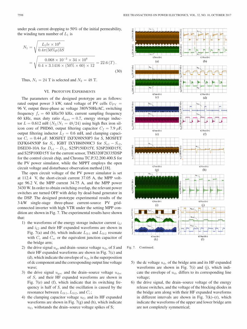
The open circuit voltage of the PV power simulator is setat 112.4 V, the short-circuit current 37.05 A, the MPP volt-age 96.2 V, the MPP current 34.75 A, and the MPP power3430 W. In order to obtain switching overlap, the relevant powerswitches are turned OFF with delay by dead-band generator inthe DSP. The designed prototype experimental results of the3-kW single-stage three-phase current-source PV grid-connected inverter with high VTR under the setting MPP con-dition are shown in Fig. 7. The experimental results have shownthat:
1) the waveforms of the energy storage inductor current iL1
and iL2 and their HF expanded waveforms are shown inFig. 7(a) and (b), which indicate Llk1 and Llk2 resonatewith Cs and Csc or the equivalent junction capacitor ofthe bridge arm;
2) the drive signal ugs and drain–source voltage uds of S andtheir HF expanded waveforms are shown in Fig. 7(c) and(d), which indicate the envelope of uds is the superpositionof dc component and the corresponding output line voltagewave;
3) the drive signal ugsc and the drain–source voltage udscof Sc and their HF expanded waveforms are shown inFig. 7(e) and (f), which indicate that its switching fre-quency is half of S, and the oscillation is caused by theresonance between Llk1 , Llk2 , and Cc ;
4) the clamping capacitor voltage uCc and its HF expandedwaveforms are shown in Fig. 7(g) and (h), which indicateuCc withstands the drain–source voltage spikes of S;
Fig. 7. Continued.
5) the dc voltage udc of the bridge arm and its HF expandedwaveforms are shown in Fig. 7(i) and (j), which indi-cate the envelope of udc differs to its corresponding linevoltage;
6) the drive signal, the drain–source voltage of the energyrelease switches, and the voltage of the blocking diodes inthe bridge arm along with their HF expanded waveformsin different intervals are shown in Fig. 7(k)–(r), whichindicate the waveforms of the upper and lower bridge armare not completely symmetrical;
CHEN et al.: SINGLE-STAGE THREE-PHASE CURRENT-SOURCE PHOTOVOLTAIC GRID-CONNECTED INVERTER HIGH VTR 7599
Fig. 7(a). Experimental waveforms of the inverter under setting MPP condi-tion. (a) Energy storage inductance current iL1, iL2. (b) HF expanded of iL1,iL2. (c) Drive signal ugs and drain-source voltage uds of S. (d) HF expandedof ugs, uds. (e) Drive signal ugsc and drain–source voltage udsc of Sc . (f) HFexpanded of ugsc udsc. (g) Clamping capacitance voltage uCc. (h) HF expandedof uCc, (i) DC side voltage udc of the bridge arm. (j) HF expanded of udc.(k) Drive signal ugsa1, drain-source voltage udsa1 of Sa1 and voltage uDa1 ofDa1 (l) HF expanded of udsa1, ugsa1, and uDa1 in Interval I. (m) HF expandedof udsa1, ugsa1, and uDa1 in Interval II. (n) HF expanded of udsa1,ugsa1, anduDa1 in Interval III. (o) Drive signal ugsa2, drain-source voltage udsa2 of Sa2and voltage uDa2 of Da2 . (p) HF expanded of udsa2, ugsa2, and uDa2 in IntervalIV. (q) HF expanded of udsa2, ugsa2, and uDa2 in Interval V. (r) HF expanded ofudsa2,ugsa2, and uDa2 in Interval VI. (s) Output filter capacitance voltage uCfa,uCfb, uCfc. (t) Three-phase grid-connected current ia , ib , ic and Phase-a gridvoltage ua . (u) Dynamic tracking MPPT waveforms.
7) the voltage of the output filter capacitor are shown inFig. 7(s), which indicates a good symmetry of three-phasefilter capacitor voltage;
8) the waveforms of the three-phase grid-connected currentand phase-a grid voltage are shown in Fig. 7(t), which in-dicate the three-phase grid-connected current waveforms
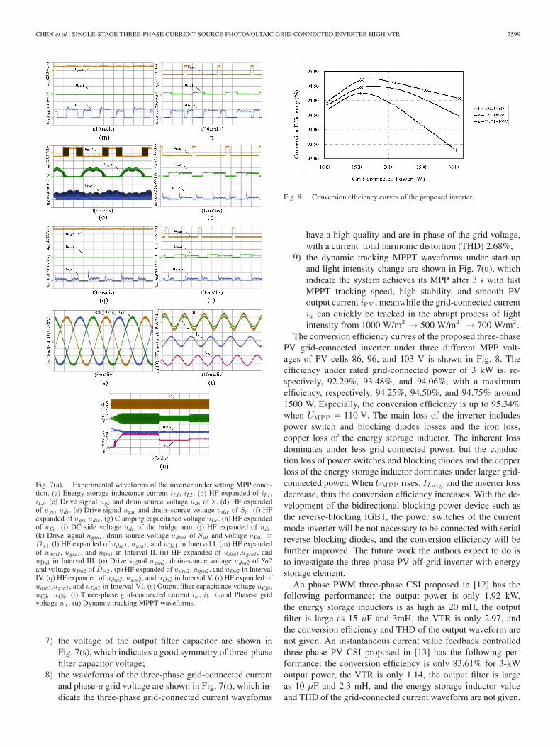
Fig. 8. Conversion efficiency curves of the proposed inverter.
have a high quality and are in phase of the grid voltage,with a current total harmonic distortion (THD) 2.68%;
9) the dynamic tracking MPPT waveforms under start-upand light intensity change are shown in Fig. 7(u), whichindicate the system achieves its MPP after 3 s with fastMPPT tracking speed, high stability, and smooth PVoutput current iPV , meanwhile the grid-connected currentia can quickly be tracked in the abrupt process of lightintensity from 1000 W/m2 → 500 W/m2 → 700 W/m2 .
The conversion efficiency curves of the proposed three-phasePV grid-connected inverter under three different MPP volt-ages of PV cells 86, 96, and 103 V is shown in Fig. 8. Theefficiency under rated grid-connected power of 3 kW is, re-spectively, 92.29%, 93.48%, and 94.06%, with a maximumefficiency, respectively, 94.25%, 94.50%, and 94.75% around1500 W. Especially, the conversion efficiency is up to 95.34%when UMPP = 110 V. The main loss of the inverter includespower switch and blocking diodes losses and the iron loss,copper loss of the energy storage inductor. The inherent lossdominates under less grid-connected power, but the conduc-tion loss of power switches and blocking diodes and the copperloss of the energy storage inductor dominates under larger grid-connected power. When UMPP rises, ILavg and the inverter lossdecrease, thus the conversion efficiency increases. With the de-velopment of the bidirectional blocking power device such asthe reverse-blocking IGBT, the power switches of the currentmode inverter will be not necessary to be connected with serialreverse blocking diodes, and the conversion efficiency will befurther improved. The future work the authors expect to do isto investigate the three-phase PV off-grid inverter with energystorage element.
An phase PWM three-phase CSI proposed in [12] has thefollowing performance: the output power is only 1.92 kW,the energy storage inductors is as high as 20 mH, the outputfilter is large as 15 μF and 3mH, the VTR is only 2.97, andthe conversion efficiency and THD of the output waveform arenot given. An instantaneous current value feedback controlledthree-phase PV CSI proposed in [13] has the following per-formance: the conversion efficiency is only 83.61% for 3-kWoutput power, the VTR is only 1.14, the output filter is largeas 10 μF and 2.3 mH, and the energy storage inductor valueand THD of the grid-connected current waveform are not given.
7600 IEEE TRANSACTIONS ON POWER ELECTRONICS, VOL. 32, NO. 10, OCTOBER 2017
A grid-connected current dynamic prediction optimization con-trolled three-phase PV CSI proposed in [14] has the followingperformance: the output power is only 2.03 kW, energy storageinductor value is as high as 15 mH, the VTR is only 1.61, theoutput waveform THD is 5.0%, and the conversion efficiency isnot given. The three-phase CSI discussed in [15] has the follow-ing performance: the output power is only 2.0 kW, the energystorage inductor is as high as 10 mH, and the output filter is largeas 20 μF and 7.5 mH, the VTR is 3.2, the output waveform THDis 5.0%, and the conversion efficiency is not given. A modifiedsingle-stage three-phase CSI presented in [16] has the followingperformance: the output power is only 0.5 kW, the VTR is 2.0,the output waveform THD is 4.5%, and the conversion efficiencyand THD of the output waveform are not given. A single-stageCSI proposed in [17] has the following performance: the outputpower is only 2.0 kW, the energy storage inductor is as high as 10mH, the VTR is 3.2, the output inductor filter is large as 20 mH,the output waveform THD is 4.1%, and the conversion efficiencyis not given. The two-stage three-phase current/voltage sourcePV inverters discussed in [19] and [20] have the following per-formance: the energy storage inductor is as high as 2.42 or 3.0mH, the VTR is 0.99 or 0.95, the output filter is large as 5 μF and6 or 5 mH, and the second conversion efficiency is 90.94%, andTHD of the output waveform is not given. Comparison resultsshow that the proposed inverter has the excellent performances,namely, higher VTR, much smaller energy storage inductor andhigher conversion efficiency. Moreover, it has lower output cur-rent THD than that of [12]–[17] and [20] and smaller outputCL filter than that of [12]–[13], [15]–[17], and [19]–[20], yet ithas larger output power than that of [12], [14]–[17], and [20].When the turns ratio N2/N1 of L is larger, the proposed inverterwill have higher VTR. While lower PV voltage can be single-stage boosted and inverted into the rated grid voltage, the volt-age configuration of the PV cells is flexible, which is the majorachievement in this paper compared to current PV inverters frompeers.
VII. CONCLUSION
1) The circuit topology of the proposed inverter is a sequen-tially cascaded of the input filter capacitor, the center-tapped energy storage inductor, three-phase invertingbridge with six serial blocking diodes, and output CL fil-ter, with an energy storage switch connected between thecenter tap of L and the negative end of the input source.
2) The proposed two-loop improved zone SPWM controlstrategy can ensure the normal operation of the CSI in anyHF switching period with the condition that output linevoltage are not smaller than input voltage, i.e.,
√6/2Up ≥
UPV , and the reactive power adjustment of the system isrealized.
3) There are six operating intervals in one output line fre-quency period, each operating interval has three operatingmodes; the VTR expression is derived, which can be ad-justed through the coefficient K = kILavg and the turnsratio N2/N1 of L.
4) The active clamped subcircuit can effectively suppress theturn-off voltage spike of S caused by the leakage inductor,and there are 14 different operating intervals within oneHF switching period Ts .
5) The design criterion of the center-tapped energy storageinductor is derived.
6) The designed 3-kW 96VDC/380V50Hz3ϕAC PV grid-connected inverter prototype has excellent performancessuch as higher VTR, much smaller energy storage inductorand higher conversion efficiency, and the experimentalresults validate theoretical analysis.
REFERENCES
[1] T. K. S. Freddy, N. A. Rahim, W. P. Hew, and H. S. Che, “Modulationtechniques to reduce leakage current in three-phase transformerless H7photovoltaic inverter,” IEEE Trans. Ind. Electron., vol. 62, no. 1, pp. 322–331, Jan. 2015.
[2] T. Messo, J. Jokipii, J. Puukko, and T. Suntio, “Determining the valueof DC-link capacitor to ensure stable operation of a three-phase photo-voltaic inverter,” IEEE Trans. Power Electron., vol. 29, no. 2, pp. 665–673,Feb. 2014.
[3] J. Ji et al., “A simple differential mode EMI Suppressor for the LLCL-filter-based single-phase grid-tied transformerless inverter,” IEEE Trans.Ind. Electron., vol. 62, no. 7, pp. 4141–4147, Jul. 2015.
[4] I. Serban, “Power decoupling method for single-phase H-bridge inverterswith no additional power electronics,” IEEE Trans. Ind. Electron., vol. 62,no. 8, pp. 4805–4813, Aug. 2015.
[5] B. Singh, C. Jain, and S. Goel, “ILST control algorithm of single-stage dualpurpose grid connected solar PV system,” IEEE Trans. Power Electron.,vol. 29, no. 10, pp. 5347–5357, Oct. 2014.
[6] D. Barater, G. Buticchi, E. Lorenzani, and C. Concari, “Active common-mode filter for ground leakage current reduction in grid-connected PVconverters operating with arbitrary power factor,” IEEE Trans. Ind. Elec-tron., vol. 61, no. 8, pp. 3940–3950, Aug. 2014.
[7] L. S. Garcia et al., “Modeling and control of a single-stage current sourceinverter with amplified sinusoidal output voltage,” in Proc. IEEE Appl.Power Electron. Conf., 2012, pp. 2024–2031.
[8] R. T. H. Li, H. S. H. Chung, and T. K. M. Chan, “An active modula-tion technique for single-phase grid-connected CSI,” IEEE Trans. PowerElectron., vol. 22, no. 4, pp. 1373–1382, Jul. 2007.
[9] D. Chen, Y. Qiu, Y. Chen, and Y. He, “Nonlinear PWM-controlled single-phase boost mode grid-connected photovoltaic inverter with limited stor-age inductance current,” IEEE Trans. Power Electron., vol. 32, no. 4,pp. 2717–2727, Apr. 2017.
[10] B. N. Alajmi, K. H. Ahmed, G. P. Adam, and B. W. Williams, “Single-phase single-stage transformer less grid-connected PV system,” IEEETrans. Power Electron., vol. 28, no. 6, pp. 2264–2676, Jun. 2013.
[11] D. Chen and Y. Chen, “Step-up AC voltage regulators with high-frequencylink,” IEEE Trans. Power Electron., vol. 28, no. 1, pp. 390–397, Jan.2013.
[12] M. Saghaleini and B. Mirafrazl, “Reactive power control in three-phasegrid-connected current source boost inverter,” in Proc. IEEE Appl. PowerElectron. Conf., 2012, pp. 904–910.
[13] A. Kavimandan and S. P. Das, “Control and protection strategy for athree-phase single-stage boost type grid-connected current source in-verter for PV applications,” in Proc. IEEE Int. Conf. Ind. Technol., 2013,pp. 1722–1727.
[14] Y. Li, P. Li, Y. Chen, and D. Zhang, “Single-stage three-phase current-source inverter for photovoltaic grid-connected system,” in Proc. 16th Eur.Conf. Power Electron. Appl., 2014, pp. 1–9.
[15] A. Singh, A. K. Kaviani, and B. Mirafzal, “On dynamic models andstability analysis of three-phase phasor PWM-based CSI for stand-aloneapplications,” IEEE Trans. Ind. Electron., vol. 62, no. 5, pp. 2698–2707,May 2015.
[16] B. Eskandari and M. T. Bina, “Support vector regression-based distor-tion compensator for three-phase DC-AC boost-inverters: Analysis andexperiments,” IET Trans. Power Electron., vol. 7, no. 2, pp. 251–258,Feb. 2014.
[17] A. Singh, A. A. Milani, and B. Mirafzal, “Modified phasor pulse widthmodulation method for three-phase single-stage boost inverter,” in Proc.IEEE Appl. Power Electron. Conf., 2014, pp. 1276–1280.

CHEN et al.: SINGLE-STAGE THREE-PHASE CURRENT-SOURCE PHOTOVOLTAIC GRID-CONNECTED INVERTER HIGH VTR 7601
[18] C. C. Hua, W. T. Chen, and Y. H. Fang, “A hybrid MPPT with adaptivestep-size based on single sensor for photovoltaic systems,” in Proc. Int.Conf. Inf. Sci. Electron. Elect. Eng., 2014, pp. 441–445.
[19] C. Jain and B. Singh, “A three-phase grid tied SPV system with adaptiveDC link voltage for CPI voltage variations,” IEEE Trans. Sustain. Energy,vol. 7, no. 1, pp. 337–344, Jan. 2016.
[20] M. C. Cavalcanti, F. Bradaschia, P. E. P. Ferraz, and L. R. Limongi,“Two-stage converter with remote state pulse width modulation for trans-formerless photovoltaic systems,” Elect. Power Syst. Res., vol. 108, no. 3,pp. 260–268, Mar. 2014.
Daolian Chen (SM’08) was born in Fujian, China, in1964. He received the B.S., M.S., Ph.D. degrees andPostdoctoral Certification from the Department ofElectrical Engineering, Nanjing University of Aero-nautics and Astronautics (NUAA), Nanjing, China,in 1986, 1989, 1998, and 2001, respectively.
He was a Teaching Assistant, a Lecturer, an Asso-ciated Professor, and a Professor with the Departmentof Electrical Engineering, NUAA, in 1989, 1991,1996, and 2002, respectively. He has been a Professorwith the College of Electrical Engineering, Fuzhou
University, Fuzhou, China, since 2005. He has been a “National Class Expertof the Hundred, Thousand, and Ten Thousand Talent Project,” “Delta Scholar,”and “National outstanding professional and technical personnel”, China, since2009, 2014, and 2014. He has been a Director of the Fujian Key Laboratory ofNew Energy Generation and Power Conversion, Fuzhou University, since 2015.He has published three works and more than 100 technical papers. He is theholder of 20 invention patents. His research interests include power electronicsconversion, new energy source generating, and aviation electrical power supplysystems.
Dr. Chen received one national and three province class reward productionsof science and technology.
Jiahui Jiang was born in Fujian, China, in 1989. Hereceived the B.S. degree from the College of Electri-cal Engineering, Fuzhou University, Fuzhou, China,in 2012, where he is currently working toward thePh.D. degree with the Fujian Key Laboratory of NewEnergy Generation and Power Conversion.
He has published several technical papers. Hisresearch interests mainly include new energy sourcegenerating system.
Yanhui Qiu was born in Fujian, China, in 1988. Hereceived the B.S. degree from the College of Electri-cal Engineering, Fuzhou University, Fuzhou, China,in 2011, where he is currently working toward thePh.D. degree with the Fujian Key Laboratory of NewEnergy Generation and Power Conversion.
He has published several technical papers. Hisresearch interests mainly include new energy sourcegenerating system.
Jie Zhang was born in Fujian, China, in 1987. Shereceived the B.S. degree from the College of Electri-cal Engineering, Fuzhou University, Fuzhou, China,in 2010, where she is currently working toward thePh.D. degree with the Fujian Key Laboratory of NewEnergy Generation and Power Conversion.
She has published several technical papers. Herresearch interests mainly include new energy sourcegenerating system.
Fusong Huang was born in Fujian, China, in 1989.He received the B.S. and M.S. degrees in electricalengineering from Fuzhou University, Fuzhou, China,in 2011 and 2014, respectively.
He is currently an Engineer in Silergy Technology,Inc., Ltd., Hangzhou, China. He has published sev-eral technical papers. His research interests mainlyinclude high-frequency power conversion.


![IEEE TRANSACTIONS ON INFORMATION FORENSICS AND …kresttechnology.com/krest-academic-projects/krest-mtech-projects/NS2... · The Unital-based key predistributed scheme (UKP) [17]](https://static.fdocuments.us/doc/165x107/5e170fc5c23381723378cf2a/ieee-transactions-on-information-forensics-and-the-unital-based-key-predistributed.jpg)


