IEEE TRANSACTIONS ON MICROWAVE THEORY …roblin/papers/2743714-class-F.pdfIEEE TRANSACTIONS ON...
11
IEEE TRANSACTIONS ON MICROWAVE THEORY AND TECHNIQUES 1 Optimal Definition of Class F for Realistic Transistor Models Francisco J. Martinez-Rodriguez, Graduate Student Member, IEEE , Patrick Roblin, Senior Member, IEEE, Zoya Popovic, Fellow, IEEE , and Jose I. Martinez-Lopez, Member, IEEE Abstract—An optimal three-harmonic definition of class F at the intrinsic level is presented for realistic transistor models exhibiting IV characteristics with a nonzero knee voltage. This updated class-F definition is needed for use with the recently reported embedding device model, which predicts in a single harmonic balance simulation the voltage and current waveforms required at the package reference planes to sustain an intrinsic mode of operation. Optimal class-F operation is obtained by setting to infinite the third-harmonic output impedance of the transistor IV characteristics instead of using an open load for the third-harmonic termination. This is achieved by fine tuning the class-F quasi-rectangular drain voltage waveform. The required third-harmonic component of the drain voltage in the optimal class F is then found to be generated by the lossless inductive termination of the third-harmonic component of the drain displacement current arising from the nonlinear drain-to-source capacitance. The proposed class-F definition is verified for a gallium nitride (GaN) high electron mobility transistor using third-harmonic load–pull simulations with a realistic GaN transistor model. The optimal third-harmonic load termination predicted using the class-F definition is found to be in full agreement with the one obtained from the drain efficiency contour plots. A close agreement is also obtained for the predicted and measured optimal third-harmonic load termination, bringing experimental support for the proposed class-F definition. Index Terms— Amplifier classes, class F, embedding device model, load pull, power amplifiers (PAs). I. I NTRODUCTION D ESIGNERS of microwave power amplifiers (PAs) have become interested in accessing the current and voltage waveforms at the transistor current-source reference planes to monitor the intrinsic mode of operation of the transistor(s) in their PA designs [1]–[3]. Indeed by optimizing the intrinsic mode of operation of the transistors, a higher power efficiency can be obtained at the device terminal levels. A novel approach for designing microwave PAs based on the characterization of the intrinsic electron-device load line using Manuscript received March 26, 2017; revised June 26, 2017; accepted July 17, 2017. This work was supported by PAPIIT under Grant IN115016. (Corresponding author: Patrick Roblin.) F. J. Martinez-Rodriguez is with the Department of Electrical and Computer Engineering, The Ohio State University, Columbus, OH 43210 USA, on leave from the Department of Electronic Engineering, National University of Mexico, Mexico City 04510, Mexico. P. Roblin is with the Department of Electrical and Computer Engi- neering, The Ohio State University, Columbus, OH 43210 USA (e-mail: [email protected]). Z. Popovic is with the Department of Electrical and Computer Engineering, University of Colorado Boulder, Boulder, CO 80309 USA. J. I. Martinez-Lopez is with the Department of Electronic Engineering, National University of Mexico, Mexico City 04510, Mexico. Color versions of one or more of the figures in this paper are available online at http://ieeexplore.ieee.org. Digital Object Identifier 10.1109/TMTT.2017.2743714 nonlinear embedding was proposed and demonstrated in [4]. With the embedding device model introduced in [5], it became possible for PA designers to directly control, within the confine of the simulation environment, the intrinsic operation mode of the device at the current-source reference planes while the required multiharmonic load and source impedance terminations at the package reference planes (device terminals) were simultaneously determined [6], [7]. Time-consuming source- and load–pull simulations are no longer needed since the optimal multiharmonic source and load impedance terminations are obtained in a single simulation. Note that the embedding device model has the further advantage of being less prone to convergence issues compared with the device model. The design of amplifiers of various classes and architectures such as Doherty, Chireix, or broadband class-J PAs designed using an embedding device model has been demonstrated in [8]– [10]. Within the various modes of operation, class F remains of great interest, as among other things, it permits the realization of Doherty and Chireix PAs that exhibit a high efficiency at both peak and backoff. Since its initial proposal in the late 1910s [11], [12], and its detailed description in [13], class F (named as such by Raab [14]) has been the object of many theoretical investigations [15]–[20], practical implementations, and experimental investigations [21]–[23] to quote a few recent examples. The initial class-F theoretical investigations [15]–[17] relied on a zero-knee voltage model for the transistor and established the theoretical performance for an ideal device, while more realistic IV models were used in [18] and [20]. The importance of clipping was highlighted using load–pull measurements in a recent study of continuous class-F PAs [23]. Finally, it is to be noted that it was proposed in [20] that the second harmonic could be optimized in class-F PAs with the help of the nonlinear drain capacitance. Given that the design of class-F PAs can now be greatly facilitated with the use of the embedding device model, it is beneficial to revisit the class-F definition for ideal devices in order to introduce an optimized version for the case of realistic IV characteristics. In a classic paper on class F [17], it is stated that “class F is probably the oldest technique for improving the efficiency of an RF PA, but is perhaps also the least well understood.” Cripps [24] refers to the “great class-F puzzle.” In this section, we shall elaborate on the motivation for these comments. The required waveforms for class-F operation are well established for the ideal FET device that features a con- stant transductance with an abrupt threshold and zero knee voltage (V ON = 0) [17]. Ideally, the class-F waveforms 0018-9480 © 2017 IEEE. Personal use is permitted, but republication/redistribution requires IEEE permission. See http://www.ieee.org/publications_standards/publications/rights/index.html for more information.
Transcript of IEEE TRANSACTIONS ON MICROWAVE THEORY …roblin/papers/2743714-class-F.pdfIEEE TRANSACTIONS ON...

IEEE TRANSACTIONS ON MICROWAVE THEORY AND TECHNIQUES 1
Optimal Definition of Class F forRealistic Transistor Models
Francisco J. Martinez-Rodriguez, Graduate Student Member, IEEE, Patrick Roblin, Senior Member, IEEE,Zoya Popovic, Fellow, IEEE, and Jose I. Martinez-Lopez, Member, IEEE
Abstract— An optimal three-harmonic definition of class F atthe intrinsic level is presented for realistic transistor modelsexhibiting IV characteristics with a nonzero knee voltage. Thisupdated class-F definition is needed for use with the recentlyreported embedding device model, which predicts in a singleharmonic balance simulation the voltage and current waveformsrequired at the package reference planes to sustain an intrinsicmode of operation. Optimal class-F operation is obtained bysetting to infinite the third-harmonic output impedance of thetransistor IV characteristics instead of using an open loadfor the third-harmonic termination. This is achieved by finetuning the class-F quasi-rectangular drain voltage waveform.The required third-harmonic component of the drain voltagein the optimal class F is then found to be generated by thelossless inductive termination of the third-harmonic componentof the drain displacement current arising from the nonlineardrain-to-source capacitance. The proposed class-F definition isverified for a gallium nitride (GaN) high electron mobilitytransistor using third-harmonic load–pull simulations with arealistic GaN transistor model. The optimal third-harmonic loadtermination predicted using the class-F definition is found to bein full agreement with the one obtained from the drain efficiencycontour plots. A close agreement is also obtained for the predictedand measured optimal third-harmonic load termination, bringingexperimental support for the proposed class-F definition.
Index Terms— Amplifier classes, class F, embedding devicemodel, load pull, power amplifiers (PAs).
I. INTRODUCTION
DESIGNERS of microwave power amplifiers (PAs) havebecome interested in accessing the current and voltage
waveforms at the transistor current-source reference planes tomonitor the intrinsic mode of operation of the transistor(s)in their PA designs [1]–[3]. Indeed by optimizing the intrinsicmode of operation of the transistors, a higher power efficiencycan be obtained at the device terminal levels.
A novel approach for designing microwave PAs based on thecharacterization of the intrinsic electron-device load line using
Manuscript received March 26, 2017; revised June 26, 2017; acceptedJuly 17, 2017. This work was supported by PAPIIT under Grant IN115016.(Corresponding author: Patrick Roblin.)
F. J. Martinez-Rodriguez is with the Department of Electrical and ComputerEngineering, The Ohio State University, Columbus, OH 43210 USA, onleave from the Department of Electronic Engineering, National Universityof Mexico, Mexico City 04510, Mexico.
P. Roblin is with the Department of Electrical and Computer Engi-neering, The Ohio State University, Columbus, OH 43210 USA (e-mail:[email protected]).
Z. Popovic is with the Department of Electrical and Computer Engineering,University of Colorado Boulder, Boulder, CO 80309 USA.
J. I. Martinez-Lopez is with the Department of Electronic Engineering,National University of Mexico, Mexico City 04510, Mexico.
Color versions of one or more of the figures in this paper are availableonline at http://ieeexplore.ieee.org.
Digital Object Identifier 10.1109/TMTT.2017.2743714
nonlinear embedding was proposed and demonstrated in [4].With the embedding device model introduced in [5], it becamepossible for PA designers to directly control, within theconfine of the simulation environment, the intrinsic operationmode of the device at the current-source reference planeswhile the required multiharmonic load and source impedanceterminations at the package reference planes (device terminals)were simultaneously determined [6], [7]. Time-consumingsource- and load–pull simulations are no longer neededsince the optimal multiharmonic source and load impedanceterminations are obtained in a single simulation. Note thatthe embedding device model has the further advantage ofbeing less prone to convergence issues compared with thedevice model. The design of amplifiers of various classes andarchitectures such as Doherty, Chireix, or broadband class-JPAs designed using an embedding device model has beendemonstrated in [8]– [10].
Within the various modes of operation, class F remainsof great interest, as among other things, it permits therealization of Doherty and Chireix PAs that exhibit a highefficiency at both peak and backoff. Since its initial proposalin the late 1910s [11], [12], and its detailed descriptionin [13], class F (named as such by Raab [14]) has been theobject of many theoretical investigations [15]–[20], practicalimplementations, and experimental investigations [21]–[23]to quote a few recent examples. The initial class-F theoreticalinvestigations [15]–[17] relied on a zero-knee voltage modelfor the transistor and established the theoretical performancefor an ideal device, while more realistic IV models were usedin [18] and [20]. The importance of clipping was highlightedusing load–pull measurements in a recent study of continuousclass-F PAs [23]. Finally, it is to be noted that it was proposedin [20] that the second harmonic could be optimized in class-FPAs with the help of the nonlinear drain capacitance.
Given that the design of class-F PAs can now be greatlyfacilitated with the use of the embedding device model, it isbeneficial to revisit the class-F definition for ideal devices inorder to introduce an optimized version for the case of realisticIV characteristics. In a classic paper on class F [17], it is statedthat “class F is probably the oldest technique for improvingthe efficiency of an RF PA, but is perhaps also the least wellunderstood.” Cripps [24] refers to the “great class-F puzzle.”In this section, we shall elaborate on the motivation for thesecomments.
The required waveforms for class-F operation are wellestablished for the ideal FET device that features a con-stant transductance with an abrupt threshold and zero kneevoltage (VON = 0) [17]. Ideally, the class-F waveforms
0018-9480 © 2017 IEEE. Personal use is permitted, but republication/redistribution requires IEEE permission.See http://www.ieee.org/publications_standards/publications/rights/index.html for more information.
2 IEEE TRANSACTIONS ON MICROWAVE THEORY AND TECHNIQUES
consist of a rectangular drain voltage waveform (withmin[vDS] = VON) and an ideal half-rectified drain currentsinewave such that the current–voltage product remains nullat all times. In the case of vanishing on-voltage, this yieldstheoretically 100% efficiency. In practice, only three har-monics (higher harmonics shorted) are usually considered.For an ideal device with zero knee voltage and VDS,1approaching VDD, this yields a maximum theoretical efficiencyof 90.7% for three harmonics [24].
In the case of an ideal FET with abrupt thresholds andconstant transconductance, the ideal half-rectified currentsinewave yields only even harmonics (see [17]), and thepower dissipation for the odd harmonics is zero. However,when the class-F drain voltage waveforms are applied torealistic FET devices with nonzero on-voltage and a nonlinearsubthreshold region, odd-harmonic drain-current componentsare generated and the transistor current source can eitherdissipate (active load) or generate power (passive load) at eachof the odd harmonics. In this paper, we will demonstrate thatto sustain class-F operation with zero power dissipation at thethird harmonic, we can simply tune the class-F waveformso that the power generation by the transistor at the thirdharmonic is null.
Let us now address the issue of the impedance load-ing required to sustain the class-F drain voltage waveform.The well-known loading conditions for class-F operationat the current-source level are the following for each har-monic n [13], [16]:
Z L ,n =
⎧⎪⎪⎨
⎪⎪⎩
4
π
VD,max − VON
ID,max, for n = 1
0, for even n > 0
∞, for odd n > 1 .
(1)
The short termination at the even harmonics is required sothat no even harmonic voltages appear between the drain andsource terminals. The open load at the odd harmonics is justi-fied since in the ideal linear device, there are no odd-harmonicdrain-current components supported by the ideal half-rectifiedcurrent sinewave even though odd harmonic voltages areapplied. The question arises in both ideal and real deviceson how the open load terminations at the odd harmonics cansupport the formation of the required odd-harmonic voltages.Indeed, as PA designers commonly experience, the loadingconditions defined in (1) do not usually provide the desireddrain class-F waveform for real transistors.
Let us discuss in more detail the case of devices with realis-tic IV characteristics featuring a smooth knee region (nonzeroon-voltage). As is explained in [24], “the action of the deviceknee region is to clip the peaks of the current waves, thusgenerating substantial amount of third harmonics.” It is thensuggested that the generated third-harmonic drain current canbe used to sustain the third-harmonic drain voltage usingthird-harmonic resistive loading. Examples are given in [24],and the following resistive loading equation is providedin [18] and [25]:
Z (I V )L ,3
Z (I V )L ,1
= R3
R1= −1
6
ID,1
ID,3.
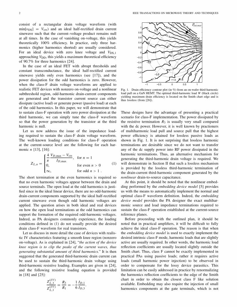
Fig. 1. Drain efficiency contour plot (in %) from an on-wafer third-harmonicload pull on a GaN HEMT. The optimal third-harmonic load W (black circle)yielding maximum drain efficiency is located on the Smith chart edge and isthus lossless (from [26]).
These designs have the advantage of presenting a practicalscenario for class-F implementation. The power dissipated bythe resistive termination R3 is usually very small comparedwith the dc power. However, it is well known by practionersof multiharmonic load pull and source pull that the highestpower efficiency is attained for lossless passive loads asshown in Fig. 1. It is not surprising that lossless harmonicterminations are desirable since we do not want to transferany of the dc supply power into RF power dissipated in theharmonic terminations. Thus, an alternative mechanism forgenerating the third-harmonic drain voltage is required. Wewill demonstrate in Section II that such a lossless mechanismis provided by the lossless third-harmonic termination ofthe drain-current third-harmonic component generated by thenonlinear drain-to-source capacitance.
At this point, it should be noted that the nonlinear embed-ding performed by the embedding device model [5] providesus with the means to automatically implement the normal andoptimal class-F waveform definition. Indeed, the embeddingdevice model provides the PA designer the exact multihar-monic source and load impedance terminations required tosustain the class-F operation established at the current-sourcereference planes.
Before proceeding with the outlined plan, it should benoted that in practical amplifiers, it will be difficult to fullyachieve the ideal class-F operation. The reason is that whenthe embedding device model is used to exactly implement thedesired intrinsic class-F mode, harmonic loads that are slightlyactive are usually required. In other words, the harmonic loadreflection coefficients are usually located slightly outside theSmith chart. Thus, class F cannot be exactly implemented inpractical PAs using passive loads; rather it requires activeloads (small harmonic power injection) to be observed inorder to compensate for the lossy device parasitics. Thislimitation can be easily addressed in practice by renormalizingthe harmonics reflection coefficients to the edge of the Smithchart in order to obtain the closest class F like solutionavailable. Embedding may also require the injection of smallharmonics components at the gate terminals, which is not
MARTINEZ-RODRIGUEZ et al.: OPTIMAL DEFINITION OF CLASS F FOR REALISTIC TRANSISTOR MODELS 3
always practical. As expected, these realizability issues leadto a reduction of a few percent in the expected efficiency. Butas we shall verify in both simulation and measurements, theseeffects are relatively small and the embedding model greatlyaccelerates the design.
This paper will present the theory and simulation veri-fications of the new optimal class-F definition for realistictransistor models in Section II. The optimal class-F designtargeted for the measurement verification will be introducedin Section III, and the measurement testbed used to experimen-tally verify it will be described in Section IV. Experimentalresults will then be presented in Section V and compared withsimulation results. Finally, in Section VI, the key results willbe discussed and summarized.
II. CLASS-F THEORY, LIMITATIONS, AND EXTENSION
In Section I, we reviewed the traditional definitions of classF based on: 1) the waveform and 2) the harmonic terminationdefinitions. We argued that each had their own advantagesand weaknesses. For the waveform class-F definition, voltagesources at the fundamental and harmonic frequencies areconnected in series between the drain and source termi-nals to apply the ideal class-F waveforms. They do not,however, automatically enforce the optimal requirement forzero odd-harmonic drain-current components, since in real-istic devices, the drain current is not a perfect half-rectifiedsinewave. The resulting odd-harmonic drain-current compo-nents flowing in the transistor current source (IV) are thenassociated with unwanted generation or dissipation (externalinjection) of harmonic power by the transistor.
In the impedance-termination class-F definition, an openload is used for the odd harmonics, and we cannot guar-anty that the desired third-harmonic voltages (VDS,n) will besustained as prescribed by the class-F waveform definition.We thus need a combination of both conditions, which isimpossible to satisfy using just the load network side, sincewe cannot simultaneously rely on the drain waveform andload impedance terminations to define passively or activelythe class-F loading. As we shall see below, one possible reso-lution of these conflicting requirements is obtained by initiallyrelying on voltage sources (at the drain terminals) to set thedesired class-F drain voltage waveform while independentlysuppressing the third harmonic of the drain current at thetransistor level by tuning the drain voltage waveform.
In the case where only three harmonics (higher harmonicsshorted) are considered, the class-F waveforms are given by
vGS = VGS − VGS,1 cos(ωt)
vDS = VDD + VDS,1 cos(ωt) + VDS,3 cos(3ωt) (2)
with VGS the dc gate bias, VGS,1 the fundamental gate volt-age (taken as positive real), VDD the dc drain bias, VDS,1 thefundamental drain voltage (taken as positive real), and VDS,3the third-harmonic drain voltage (taken as real).
The gate VGS and drain VDD dc biases and the gate VGS,1and drain VGS,1 fundamental voltages define the large signaloperating point (LSOP) for the transistor, while VDS,3 thethird-harmonic drain voltage is the perturbation defining theclass-F operation.
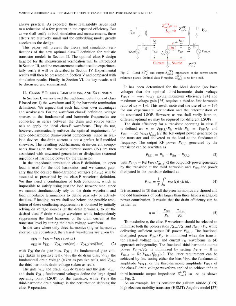
Fig. 2. Load Z (int)L ,n and output Z (I V )
out,n impedances at the current-source
reference planes. Optimal class F requires Z (I V )out,n = ∞ for n odd.
It has been determined for the ideal device (no kneevoltage) that the optimal third-harmonic drain voltageVDS,3 = −α3 VDS,1 giving maximum efficiency [24] andmaximum voltage gain [25] requires a third-to-first harmonicratio of α3 = 1/6. This result motivated the use of α3 = 1/6for our experimental verification and the determination ofits associated LSOP. However, as we shall verify later on,different optimal α3 may be required for different LSOPs.
The drain efficiency for a transistor operating in class Fis defined as: η = PRF,1/Pdc with Pdc = VDD ID andPRF,1 = Re[VDS,1 I ∗
DS,1]/2 the RF output power generated bythe transistor and delivered to the load at the fundamentalfrequency. The output RF power PRF,1 generated by thetransistor can be rewritten as
PRF,1 = Pdc − Pdiss − PRF,3 (3)
with PRF,3 = Re[VDS,3 I ∗DS,3]/2 the output RF power generated
by the transistor at the third harmonic and Pdiss the powerdissipated in the transistor defined as
Pdiss = 1
T
∫ T
0vDS(t)iD(t)dt . (4)
It is assumed in (3) that all the even harmonics are shorted andthe odd harmonics of order larger than three have a negligiblepower contribution. It results that the drain efficiency can bewritten as
η = 1 − Pdiss
Pdc− PRF,3
Pdc. (5)
To maximize η, the class-F waveform should be selected tominimize both the power ratios Pdiss/Pdc and PRF,3/Pdc whiledelivering sufficient output RF power PRF,1. The fractionaldissipated power Pdiss/Pdc is minimized when the transis-tor class-F voltage vDS and current iD waveforms in (4)approach orthogonality. The fractional third-harmonic outputpower PRF,3/Pdc is minimized by setting IDS,3 = 0 inPRF,3 = Re[VDS,3 I ∗
DS,3]/2. The latter requirement can beachieved by fine tuning either the bias VDD, the fundamentalamplitude VDS,1, or the third-harmonic amplitude VDS,3 ofthe class-F drain voltage waveform applied to achieve infinite
third-harmonic output impedance Z (I V )out,3 = ∞ as shown
in Fig. 2.As an example, let us consider the gallium nitride (GaN)
high electron mobility transistor (HEMT) Angelov model [27]

4 IEEE TRANSACTIONS ON MICROWAVE THEORY AND TECHNIQUES
Fig. 3. Variation of ID,3 and Re[Yout,3] versus the drain supply voltage VDDfor a GaN HEMT excited by a fundamental drain voltage of VDS,1 = 25.13 V.
Fig. 4. Variation of ID,3 and Re[Yout,3] versus the fundamental drainvoltage |VDS,1| for a GaN HEMT biased with a drain supply voltage ofVDD = 25 V.
extracted for the CREE CGH27015F transistor [5]. The deviceis biased with VDD = 25 V to generate about 10 W outputpower. In Figs. 3 and 4, the pure-real third-harmonic compo-nent ID,3 of the drain current and the pure-real third-harmonicoutput admittance Y (I V )
out,3 = 1/Z (I V )out,3 are plotted as a function
of the drain dc bias VDD and the pure-real fundamentalRF component VDS,1 of the applied drain-to-source voltage,respectively. As can be seen in Figs. 3 and 4, respectively,as the dc drain voltage VDD decreases or the fundamen-tal drain voltage VDS,1 increases, the third-harmonic draincurrent ID,3 and Y (I V )
out,3 switches from positive to negative.This is due to the fact that when the minima values of thedrain voltage enter the knee region of the IV, the transistorusually switches from third-harmonic power dissipation tothird-harmonic power generation. It is this feature that makesit possible to support class F without using resistive harmonicloads. Indeed, at the transition between these two modes ofoperation, the third-harmonic component of the drain currentreverses sign and thus vanishes, and no third-harmonic powerdissipation is taking place in either the transistor or the
TABLE I
SIMULATED EFFICIENCIES AS A FUNCTION OF α3FOR VDD = 25 V AND VDS,1 = 25.13 V
Fig. 5. Conventional (a) FET model and (b) embedding device model.
external load. Then there is no need to apply an open outputload at the third harmonic as specified in the conventionalclass-F harmonic impedance-termination definition, since thethird harmonic current ID,3 is already zero. Thus, instead ofrequiring an open load for the third harmonic load Z (int)
L ,3 , it is
the third-harmonic output impedance Z (I V )out,3 of the transistor
that must be set to infinite.In the above examples, α3 equal to 1/6 (optimal value
for the ideal device) was used and the LSOP was tuned viaVDD or VDS,1 to achieve Z (I V )
out,3 = ∞. Alternately given anoptimal LSOP, we can tune the perturbative third-harmonicvoltage VDS,3 or equivalently α3 to achieve Z (I V )
out,3 = ∞. As isdemonstrated in Table I for the previous LSOP example withVDD = 25 V and VDD = 25.13 V, the fractional dissipatedpower Pdiss/Pdc switches for positive to negative when α3becomes larger than 1/6 � 0.16666 and |�L ,3| becomes largerthan one. The efficiencies η and η(P) at the current-sourceand package reference planes, respectively, are both seen toincrease as α3 increases.
The drain voltage waveforms or drain loads that must beapplied at the package reference planes to sustain the requiredthird harmonic drain voltage VD,3 at the intrinsic terminalscan then be determined using the embedding device model.Two equivalent approaches are possible. The first approachrelies simply on applying the desired class-F waveform of (2)while the second approach examines the physical processsustaining the class-F waveform by determining the requiredthird-harmonic impedance terminations at the intrinsic refer-ence planes. Both methods are equivalent and yield the sameresults but require different embedding device models as weshall see. The first method is straightforward given we havealready determined the optimal drain voltage (dc, fundamental,and third harmonic) sustaining the new optimized class Fintrinsically. The conventional embedding device model shownin Fig. 5 will then determine the required multiharmonicimpedance terminations at the package or connector levelsto achieve this optimized intrinsic class-F mode. The secondapproach, to be described next, has the advantage of revealing
MARTINEZ-RODRIGUEZ et al.: OPTIMAL DEFINITION OF CLASS F FOR REALISTIC TRANSISTOR MODELS 5
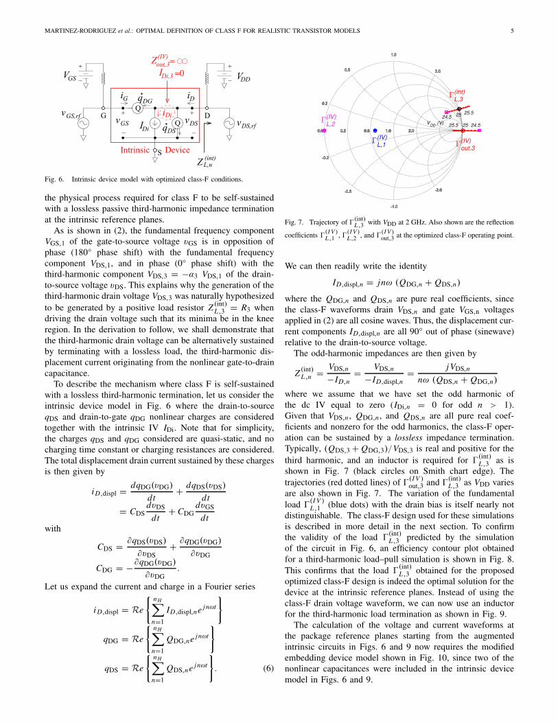
Fig. 6. Intrinsic device model with optimized class-F conditions.
the physical process required for class F to be self-sustainedwith a lossless passive third-harmonic impedance terminationat the intrinsic reference planes.
As is shown in (2), the fundamental frequency componentVGS,1 of the gate-to-source voltage vGS is in opposition ofphase (180° phase shift) with the fundamental frequencycomponent VDS,1, and in phase (0° phase shift) with thethird-harmonic component VDS,3 = −α3 VDS,1 of the drain-to-source voltage vDS. This explains why the generation of thethird-harmonic drain voltage VDS,3 was naturally hypothesizedto be generated by a positive load resistor Z (int)
L ,3 = R3 whendriving the drain voltage such that its minima be in the kneeregion. In the derivation to follow, we shall demonstrate thatthe third-harmonic drain voltage can be alternatively sustainedby terminating with a lossless load, the third-harmonic dis-placement current originating from the nonlinear gate-to-draincapacitance.
To describe the mechanism where class F is self-sustainedwith a lossless third-harmonic termination, let us consider theintrinsic device model in Fig. 6 where the drain-to-sourceqDS and drain-to-gate qDG nonlinear charges are consideredtogether with the intrinsic IV IDi. Note that for simplicity,the charges qDS and qDG considered are quasi-static, and nocharging time constant or charging resistances are considered.The total displacement drain current sustained by these chargesis then given by
iD,displ = dqDG(vDG)
dt+ dqDS(vDS)
dt
= CDSdvDS
dt+ CDG
dvGS
dtwith
CDS = ∂qDS(vDS)
∂vDS+ ∂qDG(vDG)
∂vDG
CDG = −∂qDG(vDG)
∂vDG.
Let us expand the current and charge in a Fourier series
iD,displ = Re
{nH∑
n=1
ID,displ,ne jnωt
}
qDG = Re
{nH∑
n=1
QDG,ne jnωt
}
qDS = Re
{nH∑
n=1
QDS,ne jnωt
}
. (6)
Fig. 7. Trajectory of �(int)L ,3 with VDD at 2 GHz. Also shown are the reflection
coefficients �(I V )L ,1 , �
(I V )L ,2 , and �
(I V )out,3 at the optimized class-F operating point.
We can then readily write the identity
ID,displ,n = jnω (QDG,n + QDS,n)
where the QDG,n and QDS,n are pure real coefficients, sincethe class-F waveforms drain VDS,n and gate VGS,n voltagesapplied in (2) are all cosine waves. Thus, the displacement cur-rent components ID,displ,n are all 90◦ out of phase (sinewave)relative to the drain-to-source voltage.
The odd-harmonic impedances are then given by
Z (int)L ,n = VDS,n
−ID,n= VDS,n
−ID,displ,n= j VDS,n
nω (QDS,n + QDG,n)
where we assume that we have set the odd harmonic ofthe dc IV equal to zero (IDi,n = 0 for odd n > 1).Given that VDS,n , QDG,n , and QDS,n are all pure real coef-ficients and nonzero for the odd harmonics, the class-F oper-ation can be sustained by a lossless impedance termination.Typically, (QDS,3 + QDG,3)/VDS,3 is real and positive for thethird harmonic, and an inductor is required for �
(int)L ,3 as is
shown in Fig. 7 (black circles on Smith chart edge). Thetrajectories (red dotted lines) of �
(I V )out,3 and �
(int)L ,3 as VDD varies
are also shown in Fig. 7. The variation of the fundamentalload �
(I V )L ,1 (blue dots) with the drain bias is itself nearly not
distinguishable. The class-F design used for these simulationsis described in more detail in the next section. To confirmthe validity of the load �
(int)L ,3 predicted by the simulation
of the circuit in Fig. 6, an efficiency contour plot obtainedfor a third-harmonic load–pull simulation is shown in Fig. 8.This confirms that the load �
(int)L ,3 obtained for the proposed
optimized class-F design is indeed the optimal solution for thedevice at the intrinsic reference planes. Instead of using theclass-F drain voltage waveform, we can now use an inductorfor the third-harmonic load termination as shown in Fig. 9.
The calculation of the voltage and current waveforms atthe package reference planes starting from the augmentedintrinsic circuits in Figs. 6 and 9 now requires the modifiedembedding device model shown in Fig. 10, since two of thenonlinear capacitances were included in the intrinsic devicemodel in Figs. 6 and 9.
6 IEEE TRANSACTIONS ON MICROWAVE THEORY AND TECHNIQUES
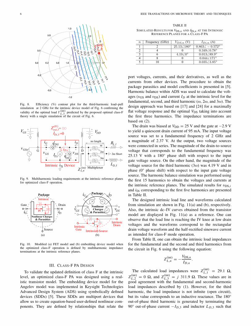
Fig. 8. Efficiency (%) contour plot for the third-harmonic load–pullsimulation at 2 GHz for the intrinsic device model of Fig. 6 confirming thevalidity of the optimal load �
(int)L ,3 predicted by the proposed optimal class-F
theory with a single simulation of the circuit of Fig. 6.
Fig. 9. Multiharmonic loading requirements at the intrinsic reference planesfor optimized class-F operation.
Fig. 10. Modified (a) FET model and (b) embedding device model whenthe optimized class-F operation is defined by multiharmonic impedanceterminations at the intrinsic reference planes.
III. CLASS-F PA DESIGN
To validate the updated definition of class F at the intrinsiclevel, an optimized class-F PA was designed using a real-istic transistor model. The embedding device model for theAngelov model was implemented in Keysight TechnologiesAdvanced Design System (ADS) using symbolically defineddevices (SDDs) [5]. These SDDs are multiport devices thatallow us to create equation-based user-defined nonlinear com-ponents. They are defined by relationships that relate the
TABLE II
SIMULATED RESULTS FOR VDS,n AND IDi,n AT THE INTRINSICREFERENCE PLANES FOR A CLASS-F PA
port voltages, currents, and their derivatives, as well as thecurrents from other devices. The procedure to obtain thepackage parasitics and model coefficients is presented in [5].Harmonic balance within ADS was used to calculate the volt-ages (vGS and vDS) and current ID at the intrinsic level for thefundamental, second, and third harmonic (ω, 2ω, and 3ω). Thedesign approach was based on [17] and [24] for a maximallyflat voltage response and the optimal VDS taking into accountthe first three harmonics. The impedance terminations arebased on (2).
The drain was biased at VDD = 25 V and the gate at −2.9 Vto yield a quiescent drain current of 95 mA. The input voltagesource was set to a fundamental frequency of 2 GHz anda magnitude of 2.37 V. At the output, two voltage sourceswere connected in series. The magnitude of the drain-to-sourcevoltage that corresponds to the fundamental frequency was25.13 V with a 180° phase shift with respect to the inputgate voltage source. On the other hand, the magnitude of thevoltage source for the third harmonic (3ω) was 4.19 V and inphase (0° phase shift) with respect to the input gate voltagesource. The harmonic balance simulation was performed usingthe first 15 harmonics to obtain the voltages and currents atthe intrinsic reference planes. The simulated results for vDS,i
and iDi corresponding to the first five harmonics are presentedin Table II.
The designed intrinsic load line and waveforms calculatedfrom simulation are shown in Fig. 11(a) and (b), respectively.Also, the intrinsic dc–IV curves obtained from the transistormodel are displayed in Fig. 11(a) as a reference. One canobserve that the load line is reaching the IV knee at low drainvoltages and the waveforms correspond to the rectangulardrain voltage waveform and the half-rectified sinewave currentas intended for class-F mode operation.
From Table II, one can obtain the intrinsic load impedancesfor the fundamental and the second and third harmonics fromthe circuit in Fig. 6 using the following equation:
Z (int)L ,n = − VDS,n
ID,n.
The calculated load impedances were Z (int)L ,1 = 29.1 �,
Z (int)L ,2 = 0 �, and Z (int)
L ,3 = j 311.9 �. These values are ingood agreement with the fundamental and second-harmonicload impedances described by (1). However, for the thirdharmonic, the load impedance is not infinite (open circuit),but its value corresponds to an inductive reactance. The 180°out-of-phase third harmonic is generated by terminating the90° out-of-phase current −ID,3 and inductor L D,3 such that

MARTINEZ-RODRIGUEZ et al.: OPTIMAL DEFINITION OF CLASS F FOR REALISTIC TRANSISTOR MODELS 7
Fig. 11. Simulated intrinsic (a) load line and (b) waveforms.
Fig. 12. Multiharmonic loads at the packaged reference planes predicted bythe embedding device model at ω, 2ω, and 3ω sustaining class-F operationat 2 GHz for the demo GaN HEMT.
we have Z (int)L ,3 = j3ωL D,3. To determine the required input
excitation or load for each harmonic at the packaged referenceplanes, an external projection of the internal operation tothe package reference planes is accomplished in a singlesimulation using the embedding device model. The resultingfundamental and harmonic loads obtained from the projectionthrough the linear extrinsic and package parasitics are shownin Fig. 12.
Note that the harmonic loads at the packaged referenceplanes are rotated and slightly outside of the Smith chart. Thiseffect can be explained due to the reactive and lossy elementsthat form both the extrinsic and package parasitics. Therefore,
TABLE III
SIMULATED EFFICIENCIES AS A FUNCTION OF α3FOR VDD = 23.2 V AND VDS,1 = 25.13 V
to obtain the desired class-F operation at the intrinsic referenceplane, the fundamental and harmonic impedance terminationsat the packaged reference planes are given by Z (pkg)
L ,1 , Z (pkg)L ,2
and Z (pkg)L ,3 . Thus, the harmonic loads should be slightly active
to synthesize the optimal mode of operation at the deviceintrinsic reference planes. In practical PA implementations,the closest passive load will be used. However, since the inten-tion of this paper is to approach the optimal class-F operation,slightly active loads were synthesized using harmonic injectionin the load–pull measurements.
The new optimized class-F design procedure was presentedhere for a GaN HEMT example. It was also verified thatsimilar results could be obtained with an SOI-MOSFETusing a previously reported ANN model [28]. An infinitethird-harmonic output impedance (Y (I V )
out,3 = 0) was obtainedat the current-source reference planes by tuning the drain biasvoltage while using α3 = 1/6. The resulting voltage andcurrent waveforms were quite similar to the GaN HEMT eventhough the drain voltage was limited to 2.5 V. An efficiencyof 67% and 60% was obtained at the current-source andpackage reference planes, respectively, while using α3 = 1/6.These results demonstrate that it is possible to use to ouradvantages the nonlinearities of the IV characteristics in othertechnologies besides GaN technologies.
In the demonstration example presented in this section,the LSOP (primarily VDD and VDS,1) is selected such thatthe third-harmonic drain voltage verifies VDS,3 = −VDS,1/6.This was motivated by the fact that α3 = 1/6 is the optimalvalue yielding the best drain efficiency for ideal devices [24].However, a different LSOP (VDD and VDS,1) could be firstselected to further reduce Pdiss/Pdc and obtain a higherdrain efficiency. The amplitude of the third-harmonic voltageVDS,3 = −α3 VDS,1 or equivalently α3 can then be tuned tominimize PRF,3 and obtain the optimal class-F operation. Thegoal is to obtain a device dynamic load line that follows theedge of the IV characteristics in the triode region more closely,by accounting for the reduction of the IV knee voltage at lowerinstantaneous gate voltages. As shown in Table III, an intrinsicefficiency above 80 % can then be achieved that way at thecurrent-source reference planes for the GaN HEMT consideredwith an optimized LSOP maintaining about the same outputpower. Similar intrinsic efficiencies around 80 % were alsoobtained for the SOI-MOSFET by jointly optimizing the LSOPand α3.
IV. MEASUREMENTS AND MEASUREMENT SETUP
In order to validate the simulated results obtainedin Section III, experiments were carried out to demonstratethe good agreement between simulated and measured results.

8 IEEE TRANSACTIONS ON MICROWAVE THEORY AND TECHNIQUES
Fig. 13. Photograph of the testbed for measuring the GaN transistor(CGH27015F).
Fig. 14. Harmonic load–pull measurement setup with an LSNA.
An active harmonic load–pull measurement setup with a large-signal network analyzer (LSNA) was used to characterizea commercially available GaN transistor CGH27015F fromCREE Semiconductors. This HEMT was originally designedfor high efficiency, high gain, and wide bandwidth capabilities.The 15-W peak power device provides in the 440166 packagea 2 W average power with 28 V drain voltage. The TRLtestbed shown in Fig. 13 was used to mount the transistor.A plastic pressure bar (not shown in Fig. 13) was used toelectrically connect the gate and drain terminal contacts to themicrostrip lines of the testbed. On the other hand, underneaththe transistor, a copper bar that acts as a heat sink is usedto connect the source terminal, which sat on a temperature-controlled thermal chuck. The measurements were performedat a chuck temperature of 10 °C.
With the help of the LSNA (MT4463A), the multiharmonicincident (a1 and a2) and the reflected (b1 and b2) waves ateach port of the device under test (DUT) were measured usingtwo directional couplers (RT0812H). These power waves alongwith the characteristic impedance of the system allow oneto calculate the magnitudes and phases of the voltages andcurrents at the testbed reference planes. The testbed or DUTis then placed on the active harmonic load–pull setup asshown in Fig. 14. The fundamental frequency (ω) of theinput signal source (Agilent ESG4438C) is set to 2 GHz.An automatic mechanical tuner connected between the inputsignal source and the testbed’s input is used to obtain theinput matching network at the fundamental. On the other hand,at the output stage, an active harmonic injection for the secondand third harmonics (2ω and 3ω) is accomplished with thehelp of two RF signal sources (Agilent ESG4438C) and atriplexer (Maury Microwave, 9677G). The triplexer is used toconnect the DUT’s output to the fundamental load as well asthe second- and third-harmonic loads. These harmonic loadsat the reference planes of the DUT’s output can be obtained bywave injection using the above-mentioned RF signal sources.
To protect the RF sources, circulators are used between eachof the signal sources and the triplexer to inject the incidentwave a2 and a3 into the DUT’s output while redirecting thereflected power wave b2 and b3 to a matched load. Two biastees are used to provide the required biasing of the transistor.A dc current meter is used to measure the drain current.
A. Experimental Conditions
Before excitations are applied to the DUT, it is important tonote that another projection of the fundamental and harmonicloads at the packaged reference planes (obtained with the helpof a linear embedding model) is required to take into accountthe transmission lines and the connectors of the testbed. TheTRL calibration method was used to characterize the errorboxes of the testbed fixture.
Initially, the transistor was biased as follows: VDD = 25 V,VGS = −2.65 V, and ID = 95 mA. The input powersource was set to an amplitude |a1(ω)| of 27 dBm witha fundamental frequency of 2 GHz. With the help of apassive tuner, the fundamental load impedance was obtainedat the connector reference plane. Two RF power sources wereused at the DUT’s output to implement harmonic injectionsat 2ω and 3ω. By controlling the corresponding harmonicmagnitude and phase of each power source, one can obtain therequired harmonic load impedances at the connector referenceplanes. A 10-MHz reference signal was used to phase-lockthe LSNA with the three RF sources. By sweeping VDDin a 24–27-V range, the best drain efficiency was obtainedat 26 V. This drain bias tuning is required to compensate forthe difference in knee voltages between the real device andthe device model used. This bias voltage was then used in therest of the measurements. In order to experimentally determinethe dependence of the drain efficiency on the third-harmonicimpedance termination, an active load–pull was implementedby changing the magnitude and phase of the power source thatinjects the signal at 3ω.
V. MEASURED RESULTS AND DISCUSSION
The resulting efficiency contour plot obtained from thethird-harmonic load pull is shown in Fig. 15. The power wavesa1, b1, a2, and b2 measured with the LSNA at the connectorreference planes were de-embedded to the package referenceplanes. The third-harmonic load reflection coefficient �
(pkg)L ,3
predicted by the embedding device model for the proposedoptimized class-F operation is also plotted (red crosses andcircles) for comparison and shown to be in good agree-ment with the load–pull measurements. This experimentallydemonstrates the accuracy of the third-harmonic impedanceprediction, as well as reveals the great time savings achievedby this methodology. Indeed the embedding process (a singlesimulation) together with the proposed class-F definitiondirectly predicts the optimal third-harmonic impedance termi-nation without the need for third-harmonic load–pulls.
The measured power waves allow us to obtain the voltagesand currents at the connector level. However, with the help ofthe deembedding transfer network, one can predict the actualharmonic drain voltage and drain current at the intrinsic ref-
MARTINEZ-RODRIGUEZ et al.: OPTIMAL DEFINITION OF CLASS F FOR REALISTIC TRANSISTOR MODELS 9
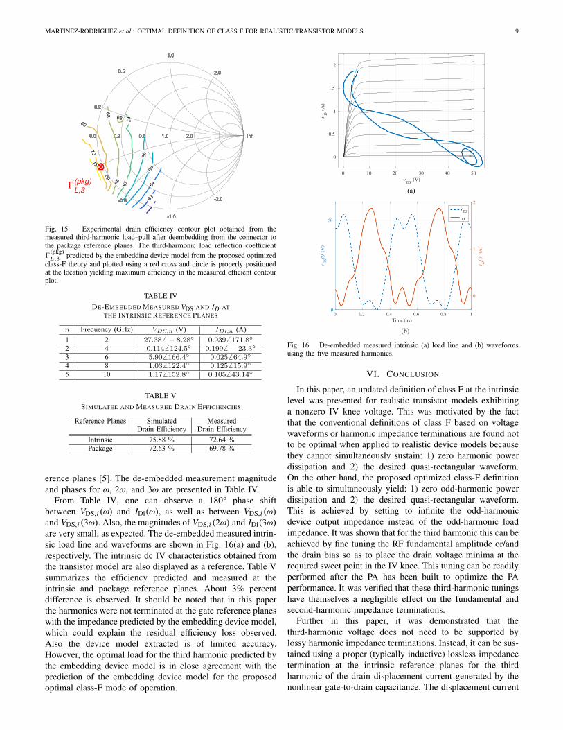
Fig. 15. Experimental drain efficiency contour plot obtained from themeasured third-harmonic load–pull after deembedding from the connector tothe package reference planes. The third-harmonic load reflection coefficient�
(pkg)L ,3 predicted by the embedding device model from the proposed optimized
class-F theory and plotted using a red cross and circle is properly positionedat the location yielding maximum efficiency in the measured efficient contourplot.
TABLE IV
DE-EMBEDDED MEASURED VDS AND ID ATTHE INTRINSIC REFERENCE PLANES
TABLE V
SIMULATED AND MEASURED DRAIN EFFICIENCIES
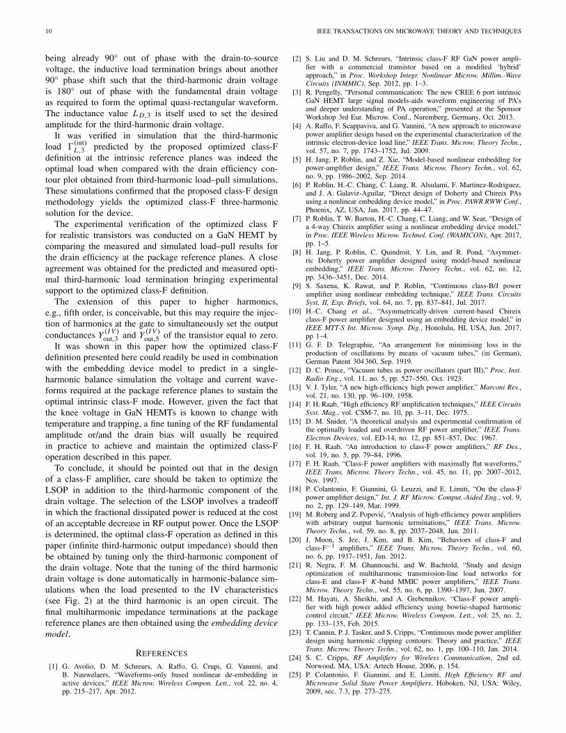
erence planes [5]. The de-embedded measurement magnitudeand phases for ω, 2ω, and 3ω are presented in Table IV.
From Table IV, one can observe a 180° phase shiftbetween VDS,i (ω) and IDi(ω), as well as between VDS,i (ω)and VDS,i (3ω). Also, the magnitudes of VDS,i (2ω) and IDi(3ω)are very small, as expected. The de-embedded measured intrin-sic load line and waveforms are shown in Fig. 16(a) and (b),respectively. The intrinsic dc IV characteristics obtained fromthe transistor model are also displayed as a reference. Table Vsummarizes the efficiency predicted and measured at theintrinsic and package reference planes. About 3% percentdifference is observed. It should be noted that in this paperthe harmonics were not terminated at the gate reference planeswith the impedance predicted by the embedding device model,which could explain the residual efficiency loss observed.Also the device model extracted is of limited accuracy.However, the optimal load for the third harmonic predicted bythe embedding device model is in close agreement with theprediction of the embedding device model for the proposedoptimal class-F mode of operation.
Fig. 16. De-embedded measured intrinsic (a) load line and (b) waveformsusing the five measured harmonics.
VI. CONCLUSION
In this paper, an updated definition of class F at the intrinsiclevel was presented for realistic transistor models exhibitinga nonzero IV knee voltage. This was motivated by the factthat the conventional definitions of class F based on voltagewaveforms or harmonic impedance terminations are found notto be optimal when applied to realistic device models becausethey cannot simultaneously sustain: 1) zero harmonic powerdissipation and 2) the desired quasi-rectangular waveform.On the other hand, the proposed optimized class-F definitionis able to simultaneously yield: 1) zero odd-harmonic powerdissipation and 2) the desired quasi-rectangular waveform.This is achieved by setting to infinite the odd-harmonicdevice output impedance instead of the odd-harmonic loadimpedance. It was shown that for the third harmonic this can beachieved by fine tuning the RF fundamental amplitude or/andthe drain bias so as to place the drain voltage minima at therequired sweet point in the IV knee. This tuning can be readilyperformed after the PA has been built to optimize the PAperformance. It was verified that these third-harmonic tuningshave themselves a negligible effect on the fundamental andsecond-harmonic impedance terminations.
Further in this paper, it was demonstrated that thethird-harmonic voltage does not need to be supported bylossy harmonic impedance terminations. Instead, it can be sus-tained using a proper (typically inductive) lossless impedancetermination at the intrinsic reference planes for the thirdharmonic of the drain displacement current generated by thenonlinear gate-to-drain capacitance. The displacement current
10 IEEE TRANSACTIONS ON MICROWAVE THEORY AND TECHNIQUES
being already 90° out of phase with the drain-to-sourcevoltage, the inductive load termination brings about another90° phase shift such that the third-harmonic drain voltageis 180° out of phase with the fundamental drain voltageas required to form the optimal quasi-rectangular waveform.The inductance value L D,3 is itself used to set the desiredamplitude for the third-harmonic drain voltage.
It was verified in simulation that the third-harmonicload �
(int)L ,3 predicted by the proposed optimized class-F
definition at the intrinsic reference planes was indeed theoptimal load when compared with the drain efficiency con-tour plot obtained from third-harmonic load–pull simulations.These simulations confirmed that the proposed class-F designmethodology yields the optimized class-F three-harmonicsolution for the device.
The experimental verification of the optimized class Ffor realistic transistors was conducted on a GaN HEMT bycomparing the measured and simulated load–pull results forthe drain efficiency at the package reference planes. A closeagreement was obtained for the predicted and measured opti-mal third-harmonic load termination bringing experimentalsupport to the optimized class-F definition.
The extension of this paper to higher harmonics,e.g., fifth order, is conceivable, but this may require the injec-tion of harmonics at the gate to simultaneously set the outputconductances Y (I V )
out,3 and Y (I V )out,5 of the transistor equal to zero.
It was shown in this paper how the optimized class-Fdefinition presented here could readily be used in combinationwith the embedding device model to predict in a single-harmonic balance simulation the voltage and current wave-forms required at the package reference planes to sustain theoptimal intrinsic class-F mode. However, given the fact thatthe knee voltage in GaN HEMTs is known to change withtemperature and trapping, a fine tuning of the RF fundamentalamplitude or/and the drain bias will usually be requiredin practice to achieve and maintain the optimized class-Foperation described in this paper.
To conclude, it should be pointed out that in the designof a class-F amplifier, care should be taken to optimize theLSOP in addition to the third-harmonic component of thedrain voltage. The selection of the LSOP involves a tradeoffin which the fractional dissipated power is reduced at the costof an acceptable decrease in RF output power. Once the LSOPis determined, the optimal class-F operation as defined in thispaper (infinite third-harmonic output impedance) should thenbe obtained by tuning only the third-harmonic component ofthe drain voltage. Note that the tuning of the third harmonicdrain voltage is done automatically in harmonic-balance sim-ulations when the load presented to the IV characteristics(see Fig. 2) at the third harmonic is an open circuit. Thefinal multiharmonic impedance terminations at the packagereference planes are then obtained using the embedding devicemodel.
REFERENCES
[1] G. Avolio, D. M. Schreurs, A. Raffo, G. Crupi, G. Vannini, andB. Nauwelaers, “Waveforms-only based nonlinear de-embedding inactive devices,” IEEE Microw. Wireless Compon. Lett., vol. 22, no. 4,pp. 215–217, Apr. 2012.
[2] S. Liu and D. M. Schreurs, “Intrinsic class-F RF GaN power ampli-fier with a commercial transistor based on a modified ‘hybrid’approach,” in Proc. Workshop Integr. Nonlinear Microw. Millim.-WaveCircuits (INMMIC), Sep. 2012, pp. 1–3.
[3] R. Pengelly, “Personal communication: The new CREE 6 port intrinsicGaN HEMT large signal models-aids waveform engineering of PA’sand deeper understanding of PA operation,” presented at the SponsorWorkshop 3rd Eur. Microw. Conf., Nuremberg, Germany, Oct. 2013.
[4] A. Raffo, F. Scappaviva, and G. Vannini, “A new approach to microwavepower amplifier design based on the experimental characterization of theintrinsic electron-device load line,” IEEE Trans. Microw. Theory Techn.,vol. 57, no. 7, pp. 1743–1752, Jul. 2009.
[5] H. Jang, P. Roblin, and Z. Xie, “Model-based nonlinear embedding forpower-amplifier design,” IEEE Trans. Microw. Theory Techn., vol. 62,no. 9, pp. 1986–2002, Sep. 2014.
[6] P. Roblin, H.-C. Chang, C. Liang, R. Alsulami, F. Martinez-Rodriguez,and J. A. Galaviz-Aguilar, “Direct design of Doherty and Chireix PAsusing a nonlinear embedding device model,” in Proc. PAWR RWW Conf.,Phoenix, AZ, USA, Jan. 2017, pp. 44–47.
[7] P. Roblin, T. W. Barton, H.-C. Chang, C. Liang, and W. Sear, “Design ofa 4-way Chireix amplifier using a nonlinear embedding device model,”in Proc. IEEE Wireless Microw. Technol. Conf. (WAMICON), Apr. 2017,pp. 1–5.
[8] H. Jang, P. Roblin, C. Quindroit, Y. Lin, and R. Pond, “Asymmet-ric Doherty power amplifier designed using model-based nonlinearembedding,” IEEE Trans. Microw. Theory Techn., vol. 62, no. 12,pp. 3436–3451, Dec. 2014.
[9] S. Saxena, K. Rawat, and P. Roblin, “Continuous class-B/J poweramplifier using nonlinear embedding technique,” IEEE Trans. CircuitsSyst. II, Exp. Briefs, vol. 64, no. 7, pp. 837–841, Jul. 2017.
[10] H.-C. Chang et al., “Asymmetrically-driven current-based Chireixclass-F power amplifier designed using an embedding device model,” inIEEE MTT-S Int. Microw. Symp. Dig., Honolulu, HI, USA, Jun. 2017,pp 1–4.
[11] G. F. D. Telegraphie, “An arrangement for minimising loss in theproduction of oscillations by means of vacuum tubes,” (in German),German Patent 304 360, Sep. 1919.
[12] D. C. Prince, “Vacuum tubes as power oscillators (part III),” Proc. Inst.Radio Eng., vol. 11, no. 5, pp. 527–550, Oct. 1923.
[13] V. J. Tyler, “A new high-efficiency high power amplifier,” Marconi Rev.,vol. 21, no. 130, pp. 96–109, 1958.
[14] F. H. Raab, “High efficiency RF amplification techniques,” IEEE CircuitsSyst. Mag., vol. CSM-7, no. 10, pp. 3–11, Dec. 1975.
[15] D. M. Snider, “A theoretical analysis and experimental confirmation ofthe optimally loaded and overdriven RF power amplifier,” IEEE Trans.Electron Devices, vol. ED-14, no. 12, pp. 851–857, Dec. 1967.
[16] F. H. Raab, “An introduction to class-F power amplifiers,” RF Des.,vol. 19, no. 5, pp. 79–84, 1996.
[17] F. H. Raab, “Class-F power amplifiers with maximally flat waveforms,”IEEE Trans. Microw. Theory Techn., vol. 45, no. 11, pp. 2007–2012,Nov. 1997.
[18] P. Colantonio, F. Giannini, G. Leuzzi, and E. Limiti, “On the class-Fpower amplifier design,” Int. J. RF Microw. Comput.-Aided Eng., vol. 9,no. 2, pp. 129–149, Mar. 1999.
[19] M. Roberg and Z. Popovic, “Analysis of high-efficiency power amplifierswith arbitrary output harmonic terminations,” IEEE Trans. Microw.Theory Techn., vol. 59, no. 8, pp. 2037–2048, Jun. 2011.
[20] J. Moon, S. Jee, J. Kim, and B. Kim, “Behaviors of class-F andclass-F−1 amplifiers,” IEEE Trans. Microw. Theory Techn., vol. 60,no. 6, pp. 1937–1951, Jun. 2012.
[21] R. Negra, F. M. Ghannouchi, and W. Bachtold, “Study and designoptimization of multiharmonic transmission-line load networks forclass-E and class-F K -band MMIC power amplifiers,” IEEE Trans.Microw. Theory Techn., vol. 55, no. 6, pp. 1390–1397, Jun. 2007.
[22] M. Hayati, A. Sheikhi, and A. Grebennikov, “Class-F power ampli-fier with high power added efficiency using bowtie-shaped harmoniccontrol circuit,” IEEE Microw. Wireless Compon. Lett., vol. 25, no. 2,pp. 133–135, Feb. 2015.
[23] T. Cannin, P. J. Tasker, and S. Cripps, “Continuous mode power amplifierdesign using harmonic clipping contours: Theory and practice,” IEEETrans. Microw. Theory Techn., vol. 62, no. 1, pp. 100–110, Jan. 2014.
[24] S. C. Cripps, RF Amplifiers for Wireless Communication, 2nd ed.Norwood, MA, USA: Artech House, 2006, p. 154.
[25] P. Colantonio, F. Giannini, and E. Limiti, High Efficiency RF andMicrowave Solid State Power Amplifiers. Hoboken, NJ, USA: Wiley,2009, sec. 7.3, pp. 273–275.

MARTINEZ-RODRIGUEZ et al.: OPTIMAL DEFINITION OF CLASS F FOR REALISTIC TRANSISTOR MODELS 11
[26] X. Cui, S. J. Doo, P. Roblin, G. Jessen, R. Rojas, and J. Strahler, “Real-time active load–pull of the 2nd & 3rd harmonics for interactive designof non-linear power amplifiers,” in Proc. 68th ARFTG Conf., Boulder,CO, USA, 2006, pp. 42–49.
[27] I. Angelov, “Empirical nonlinear IV and capacitance large signal mod-els and model implementation,” in Proc. MOS-AK GSA Workshop,Dec. 2009, pp. 1–51.
[28] Y. Ko et al., “Artificial neural network model of SOS-MOSFETs basedon dynamic large-signal measurements,” IEEE Trans. Microw. TheoryTechn., vol. 62, no. 3, pp. 491–501, Mar. 2014.
Francisco J. Martinez-Rodriguez (GS’17) receivedthe B.S. degree in communications and elec-tronics engineering from the National PolytechnicInstitute, Mexico City, Mexico, in 2007, and theM.Sc. degree in electrical engineering from theNational Autonomous University of Mexico, MexicoCity, in 2014, where he is currently pursuing thePh.D. degree in electrical engineering.
From 2015 to 2017, he was a Visiting Scholar withthe Electrical and Computer Engineering Depart-ment, The Ohio State University, Columbus, OH,
USA. His current research interests include the measurement, modeling, anddesign of nonlinear RF devices such as power amplifiers.
Patrick Roblin (M’85–SM’14) was born in Paris,France, in 1958. He received the Maitrise de Physicsdegree from Louis Pasteur University, Strasbourg,France, in 1980, and the M.S. and D.Sc. degreesin electrical engineering from Washington Univer-sity, St. Louis, MO, USA, in 1982 and 1984,respectively.
In 1984, he was an Assistant Professor with theDepartment of Electrical Engineering, The OhioState University (OSU), Columbus, OH, USA,where he is currently a Professor. He is also the
Founder of the Nonlinear RF Research Laboratory, OSU. He has developedtwo educational RF/microwave laboratories and associated curriculum fortraining both undergraduate and graduate students. He is the first author of twotextbooks, High-Speed Heterostructure and Devices (Cambridge Univ. Press,2002) and Nonlinear RF Circuits and Nonlinear Vector Network Analyzers(Cambridge Univ. Press, 2011). His current research interests include themeasurement, modeling, design, and linearization of nonlinear RF devicesand circuits such as oscillators, mixers, and power amplifiers.
Dr. Roblin has been a Distinguished Microwave Lecturer since 2016.
Zoya Popovic (S’86–M’90–SM’99–F’02) receivedthe Dipl.Ing. degree from the University of Belgrade,Belgrade, Serbia, and the Ph.D. degree from the Cal-ifornia Institute of Technology, Pasadena, CA, USA.
From 2001 to 2003, she was a Visiting Pro-fessor with the Technical University of Munich,Munich, Germany, and in 2014, she was a VisitingProfessor with ISAE, Toulouse, France. She hasgraduated 56 Ph.D. students and currently advises12 doctoral students. She is a Distinguished Pro-fessor and the Lockheed Martin Endowed Chair
of Electrical Engineering with the University of Colorado, Boulder, CO,USA. Her current research interests include high-efficiency power ampli-fiers and transmitters, microwave and millimeter-wave high-performancecircuits for communications and radar, medical applications of microwaves,millimeter-wave and terahertz quasi-optical techniques, and wirelesspowering.
Dr. Popovic was a recipient of two IEEE MTT Microwave Prizes for thebest journal papers, the White House NSF Presidential Faculty Fellow Award,the URSI Issac Koga Gold Medal, the ASEE/HP Terman Medal, and theGerman Humboldt Research Award. She was elected as a Foreign Memberof the Serbian Academy of Sciences and Arts in 2006. She was named theIEEE MTT Distinguished Educator in 2013 and the University of ColoradoDistinguished Research Lecturer in 2015.
Jose I. Martinez-Lopez (M’13) was born in Mex-ico City, Mexico. He received the B.S., M.Eng.,and Ph.D. degrees in electrical engineering fromthe National Autonomous University of Mex-ico (UNAM), Mexico City, in 1994, 1998, and 2005,respectively.
He is currently a Professor of electrical engi-neering with UNAM. In 2006, he was with theSchlumberger Technology Center, Sugar Land, TX,USA, developing antennas for deep induction arraytools for the oil industry. In 2009, he was with the
ElectroScience Laboratory, The Ohio State University, Columbus, OH, USA,for one year as a Visiting Scholar. His current research interests includeantenna arrays and microwave and millimeter-wave circuits.