
IEEE TRANSACTIONS ON ELECTRON DEVICES, VOL. 50, NO. 6 ...
8
IEEE TRANSACTIONS ON ELECTRON DEVICES, VOL. 50, NO. 6, JUNE 2003 1467 Modeling of Grain Growth Mechanism by Nickel Silicide Reactive Grain Boundary Effect in Metal-Induced-Lateral-Crystallization C. F. Cheng, Vincent M. C. Poon, Senior Member, IEEE, C. W. Kok, Senior Member, IEEE, and Mansun Chan, Senior Member, IEEE Abstract—The growth mechanism of metal-induced-lat- eral-crystallization (MILC) was studied and modeled. Based on the time evolution of the metal impurity in the amorphous silicon film being crystallized, a model has been developed to predict the growth rate and the final metal distribution in the crystallized polysilicon. The model prediction has been compared with experimental results and high prediction accuracy is demon- strated. Using the model, the effects of annealing temperature, annealing time and initial metal concentration on the final grain size and metal impurity distribution can be analyzed. As a result, the model can be used to optimize the grain growth conditions for fabricating high performance thin-film-transistors on the recrystallized polysilicon film. Index Terms—Crystallization, grain growth, polysilicon, thin-film transistor. I. INTRODUCTION T HE application of metal-induced-lateral-crystallization (MILC) using nickel has recently been shown to be an effective method for synthesizing large grain size polysilicon that can be used to fabricate high quality thin-film transistor (TFT) [1]–[3]. The final performance of the fabricated TFT, however, strongly depends on the size and structure of the grain in the recrystallized polysilicon film as well as the final distribution of nickel atoms [4]. With different combinations of grain structure and the TFT size, the amount and orientation of grain boundaries in the active area of the transistors vary [5], [6]. These grain boundaries cause a gentler turn on and lower carrier drift mobility in the TFT operation [7]. On the other hand, low resistivity can be obtained by adding nickel impurity into silicon layer [8]. The distribution of nickel atoms may result in some high metal concentration paths that cause high leakage current. Therefore, the study of grain structure and metal concentration of the final polysilicon film obtained from the MILC process is very important to predict the resulting TFT performance. As far as the MILC process is concerned, there is no simple reported method to predict the resulting polysilicon film quality. Manuscript received July 25, 2002; revised January 7, 2003. This work was supported by the Competitive Embarked Research Grant from the Research Grant Council of Hong Kong. The review of this paper was arranged by Ed- itor C. McAndrew. The authors are with Department of Electrical and Electronic Engineering, Hong Kong University of Science and Technology, Hong Kong (e-mail: [email protected]). Digital Object Identifier 10.1109/TED.2003.813521 Mass spectrum analysis, such as secondary ion mass spectrom- etry (SIMS), has been the most widely used method to extract the metal impurity distribution after the MILC process, which at the same time provides useful information about the grain struc- ture. But this method is a post-fabrication measurement that cannot be used to optimize the MILC process [9]. In this paper, the grain growth mechanism in the MILC process is studied. A model has been developed to predict the MILC growth rate, polysilicon grain size and final metal impurity distribution. The influence of various process parameters such as annealing tem- perature and annealing time are incorporated in the model which can be used to optimize the MILC process between MILC rate and crystal quality. Comparison of the model prediction with observed experimental results will also be given and discussed. II. MECHANISM OF MILC In the MILC process, a layer of amorphous silicon (a-Si) is first deposited on top of an insulator, usually silicon dioxide or glass. This layer of a-Si is protected by a layer of passivation oxide except at some windows where nickel is allowed to con- tact the a-Si to initiate the metal diffusion for MILC. The entire amorphous with nickel is usually annealed at a temperature be- tween 550 C and 625 C. During this MILC annealing, nickel deposited onto the seed window first reacts with silicon to form a thin nickel silicide film. This silicide layer reduces the activa- tion energy for a-Si crystallization. Thus, a-Si under the silicide is thermally crystallized into polysilicon before other part of the a-Si, and this is called the initial nucleation of crystalline Si on nickel silicide [10]. As this polysilicon is formed by a direct metal induced method, it is also referred as metal-induced-crys- tallization (MIC) polysilicon. The grain size of MIC polysilicon is bigger than that of conventional SPC polysilicon, but compar- atively smaller than that of MILC polysilicon [11]. There are many grain boundaries inside the MIC polysilicon layer [11] and these grain boundaries provide good locations for trapping the metal atoms. Due to the fast nickel diffusion in crystalline silicon structure and good nickel trapping property at the crys- talline silicon to a-Si interface [10], most of nickel atoms in the MIC region diffuse to and are trapped at the grain boundaries. The trapped metal atoms react with silicon atoms to form thin layers of nickel silicide at the grain boundaries. At the MIC to a-Si interface, the nickel silicide boundaries exist as a contin- uous sandwich layer between MIC polysilicon and a-Si as illus- trated in Fig.1 (a) and (b). This continuous nickel silicide layer 0018-9383/03$17.00 © 2003 IEEE
Transcript of IEEE TRANSACTIONS ON ELECTRON DEVICES, VOL. 50, NO. 6 ...

IEEE TRANSACTIONS ON ELECTRON DEVICES, VOL. 50, NO. 6, JUNE 2003 1467
Modeling of Grain Growth Mechanism by NickelSilicide Reactive Grain Boundary Effect in
Metal-Induced-Lateral-CrystallizationC. F. Cheng, Vincent M. C. Poon, Senior Member, IEEE, C. W. Kok, Senior Member, IEEE, and
Mansun Chan, Senior Member, IEEE
Abstract—The growth mechanism of metal-induced-lat-eral-crystallization (MILC) was studied and modeled. Basedon the time evolution of the metal impurity in the amorphoussilicon film being crystallized, a model has been developed topredict the growth rate and the final metal distribution in thecrystallized polysilicon. The model prediction has been comparedwith experimental results and high prediction accuracy is demon-strated. Using the model, the effects of annealing temperature,annealing time and initial metal concentration on the final grainsize and metal impurity distribution can be analyzed. As a result,the model can be used to optimize the grain growth conditionsfor fabricating high performance thin-film-transistors on therecrystallized polysilicon film.
Index Terms—Crystallization, grain growth, polysilicon,thin-film transistor.
I. INTRODUCTION
T HE application of metal-induced-lateral-crystallization(MILC) using nickel has recently been shown to be an
effective method for synthesizing large grain size polysiliconthat can be used to fabricate high quality thin-film transistor(TFT) [1]–[3]. The final performance of the fabricated TFT,however, strongly depends on the size and structure of thegrain in the recrystallized polysilicon film as well as the finaldistribution of nickel atoms [4]. With different combinations ofgrain structure and the TFT size, the amount and orientation ofgrain boundaries in the active area of the transistors vary [5],[6]. These grain boundaries cause a gentler turn on and lowercarrier drift mobility in the TFT operation [7]. On the otherhand, low resistivity can be obtained by adding nickel impurityinto silicon layer [8]. The distribution of nickel atoms mayresult in some high metal concentration paths that cause highleakage current. Therefore, the study of grain structure andmetal concentration of the final polysilicon film obtained fromthe MILC process is very important to predict the resultingTFT performance.
As far as the MILC process is concerned, there is no simplereported method to predict the resulting polysilicon film quality.
Manuscript received July 25, 2002; revised January 7, 2003. This work wassupported by the Competitive Embarked Research Grant from the ResearchGrant Council of Hong Kong. The review of this paper was arranged by Ed-itor C. McAndrew.
The authors are with Department of Electrical and Electronic Engineering,Hong Kong University of Science and Technology, Hong Kong (e-mail:[email protected]).
Digital Object Identifier 10.1109/TED.2003.813521
Mass spectrum analysis, such as secondary ion mass spectrom-etry (SIMS), has been the most widely used method to extractthe metal impurity distribution after the MILC process, which atthe same time provides useful information about the grain struc-ture. But this method is a post-fabrication measurement thatcannot be used to optimize the MILC process [9]. In this paper,the grain growth mechanism in the MILC process is studied.A model has been developed to predict the MILC growth rate,polysilicon grain size and final metal impurity distribution. Theinfluence of various process parameters such as annealing tem-perature and annealing time are incorporated in the model whichcan be used to optimize the MILC process between MILC rateand crystal quality. Comparison of the model prediction withobserved experimental results will also be given and discussed.
II. M ECHANISM OF MILC
In the MILC process, a layer of amorphous silicon (a-Si) isfirst deposited on top of an insulator, usually silicon dioxide orglass. This layer of a-Si is protected by a layer of passivationoxide except at some windows where nickel is allowed to con-tact the a-Si to initiate the metal diffusion for MILC. The entireamorphous with nickel is usually annealed at a temperature be-tween 550 C and 625 C. During this MILC annealing, nickeldeposited onto the seed window first reacts with silicon to forma thin nickel silicide film. This silicide layer reduces the activa-tion energy for a-Si crystallization. Thus, a-Si under the silicideis thermally crystallized into polysilicon before other part of thea-Si, and this is called the initial nucleation of crystalline Si onnickel silicide [10]. As this polysilicon is formed by a directmetal induced method, it is also referred as metal-induced-crys-tallization (MIC) polysilicon. The grain size of MIC polysiliconis bigger than that of conventional SPC polysilicon, but compar-atively smaller than that of MILC polysilicon [11]. There aremany grain boundaries inside the MIC polysilicon layer [11]and these grain boundaries provide good locations for trappingthe metal atoms. Due to the fast nickel diffusion in crystallinesilicon structure and good nickel trapping property at the crys-talline silicon to a-Si interface [10], most of nickel atoms in theMIC region diffuse to and are trapped at the grain boundaries.The trapped metal atoms react with silicon atoms to form thinlayers of nickel silicide at the grain boundaries. At the MIC toa-Si interface, the nickel silicide boundaries exist as a contin-uous sandwich layer between MIC polysilicon and a-Si as illus-trated in Fig.1 (a) and (b). This continuous nickel silicide layer
0018-9383/03$17.00 © 2003 IEEE
1468 IEEE TRANSACTIONS ON ELECTRON DEVICES, VOL. 50, NO. 6, JUNE 2003
(a)
(b)
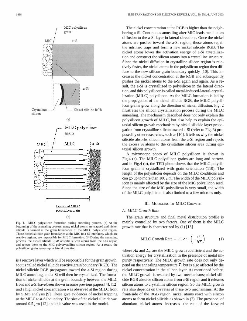
Fig. 1. MILC polysilicon formation during annealing process. (a) At thebeginning of the annealing process, many nickel atoms are trapped and nickelsilicide is formed at the grain boundaries of the MILC polysilicon region.Those nickel silicide grain boundaries at the MIC to a-Si interfaces, which arereactive regions, are responsible for MILC formation. (b) During the annealingprocess, the nickel silicide RGB absorbs silicon atoms from the a-Si regionand rejects them to the MIC polycrystalline silicon region. As a result, thepolysilicon grain grows up in lateral direction.
is a reactive layer which will be responsible for the grain growth,so it is called nickel silicide reactive grain boundary (RGB). Thenickel silicide RGB propagates toward the a-Si region duringMILC annealing, and a-Si will then be crystallized. The forma-tion of nickel silicide at the grain boundary between the MILCfront and a-Si have been shown in some previous papers [4], [12]and a high nickel concentration was observed at the MILC frontby SIMS analysis [9]. These give evidences of nickel trappingat the MILC to a-Si boundary. The size of the nickel silicide wasaround 0.5 m [12] and this value was used in the model.
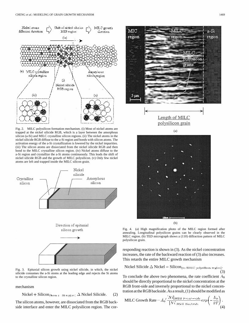
The nickel concentration at the RGB is higher than the neigh-boring a-Si. Continuous annealing after MIC leads metal atomdiffusion to the a-Si layer in lateral directions. Once the nickelatoms are pushed toward the a-Si region, those atoms repairthe intrinsic traps and form a new nickel silicide RGB. Thenickel atoms lower the activation energy of a-Si crystalliza-tion and construct the silicon atoms into a crystalline structure.Since the nickel diffusion in crystalline silicon region is rela-tively faster, the nickel atoms in the polysilicon region then dif-fuse to the new silicon grain boundary quickly [10]. This in-creases the nickel concentration at the RGB and subsequentlypushes the nickel atoms to the a-Si again and again. As a re-sult, the a-Si is crystallized to polysilicon in the lateral direc-tion, and this polysilicon is called metal-induced-lateral-crystal-lization (MILC) polysilicon. As the MILC formation is led bythe propagation of the nickel silicide RGB, the MILC polysil-icon grains grow along the direction of nickel diffusion. Fig. 2illustrates the silicon crystallization process during the MILCannealing. The mechanism described does not only explain thepolysilicon growth of MILC, but also help to explain the epi-taxial silicon growth mechanism by nickel silicide layer propa-gation from crystalline silicon toward a-Si (refer to Fig. 3) pro-posed by other researches, such as [10]. It tells us why the nickelsilicide absorbs silicon atoms from the a-Si region and rejectsthe excess Si atoms to the crystalline silicon area during epi-taxial silicon growth.
A microscope photo of MILC polysilicon is shown inFig.4 (a). The MILC polysilicon grains are long and narrow,and in Fig.4 (b), the TED photo shows that the MILC polysil-icon grain is crystallized with grain orientation (110). Thelength of the polysilicon depends on the MILC conditions andcan go up to more than 100m. The width of the MILC polysil-icon is mainly affected by the size of the MIC polysilicon seed.Since the size of the MIC polysilicon is very small, the widthof the MILC polysilicon is also limited to a few microns only.
III. M ODELING OF MILC GROWTH
A. MILC Growth Rate
The grain structure and final metal distribution profile ismainly controlled by two factors. One of them is the MILCgrowth rate that is characterized by (1) [13]
MILC Growth Rate (1)
where and are the MILC growth coefficient and the ac-tivation energy for crystallization in the presence of metal im-purity respectively. The MILC growth rate does not only de-pend on the annealing temperature, but is also affected by thenickel concentration in the silicon layer. As mentioned before,the MILC growth is resulted by two mechanisms; nickel sili-cide RGB absorbs silicon atoms from a-Si region and it releasessilicon atoms to crystalline silicon region. So the MILC growthrate also depends on the rates of these two mechanisms. At thefront-side of the RGB region, nickel atoms react with siliconatoms to form nickel silicide as shown in (2). The presence ofabundant nickel atoms increases the rate of the forward
CHENGet al.: MODELING OF GRAIN GROWTH MECHANISM 1469
Fig. 2. MILC polysilicon formation mechanism. (i) Most of nickel atoms aretrapped at the nickel silicide RGB, which is a layer between the amorphoussilicon (a-Si) and MILC crystalline silicon regions. (ii) The nickel atoms in thenickel silicide RGB diffuse to the a-Si region and bonds with silicon atoms. Theactivation energy of the a-Si crystallization is lowered by the nickel impurities.(iii) The silicon atoms are dissociated from the nickel silicide RGB and thenbond to the MILC crystalline silicon region. (iv) Nickel atoms diffuse to thea-Si region and crystallize the a-Si atoms continuously. This leads the shift ofnickel silicide RGB and the growth of MILC polysilicon. (v) Only few nickelatoms are left and trapped inside the MILC silicon grain.
Fig. 3. Epitaxial silicon growth using nickel silicide, in which, the nickelsilicide consumes the a-Si stoms at the leading edge and rejects the Si atomsto the crystalline silicon region.
mechanism
Nickel Silicon Nickel Silicide (2)
The silicon atoms, however, are dissociated from the RGB back-side interface and enter the MILC polysilicon region. The cor-
(a)
(b)
Fig. 4. (a) High magnification photo of the MILC region formed afterannealing. Longitudinal polysilicon grains can be clearly observed in theMILC region. (b) TED micrograph shows a (110) diffraction pattern of MILCpolysilicon grain.
responding reaction is shown in (3). As the nickel concentrationincreases, the rate of the backward reaction of (3) also increases.This retards the entire MILC growth mechanism
Nickel Silicide Nickel Silicon(3)
To conclude the above two phenomena, the rate coefficientshould be directly proportional to the nickel concentration at theRGB front-side and inversely proportional to the nickel concen-trationat theRGBbackside.Asa result, (1) shouldbemodifiedas
MILC Growth Rate
(4)

1470 IEEE TRANSACTIONS ON ELECTRON DEVICES, VOL. 50, NO. 6, JUNE 2003
The above growth rate equation, (4), assumes that the prop-erties and states of the a-Si do not change during the entireannealing process. However, solid-phase-crystallization (SPC)also occurs throughout the entire film that converts the a-Si topolysilicon, regardless of the presence of metal impurity. TheSPC rate is usually very slow at low temperature and the SPC ef-fect can be ignored at a temperature below 600C. When a highMILC annealing temperature C is applied to speed upthe MILC process, the SPC process becomes significant and theMILC growth rate is retarded. The growth of nano-structure ofthe a-Si to polysilicon exists as a counter-effect to MILC growth.To incorporate this effect in some intermediate and high temper-ature processing, the activation energy of a-Si crystallization isno longer a constant. A larger SPC growth rate results higheractivation energy of a-Si crystallization as
(5)
where and are the growth coefficient and the activationenergy for SPC process, respectively. The net MILC growth rateis then obtained by combining (4) and (5) as
MILC Growth Rate
(6)
It should known that and are some process dependentparameters which depend on the nature, properties, geometriesand dimensions of the a-Si layer, whereas and are acti-vation energies dependent on silicon crystallization mechanism.
B. Nickel Diffusion in the Silicon Layer
Metal diffusion is another important mechanism that affectsthe final silicon film quality after recrystallization. In particular,the diffusion of nickel in amorphous and polycrystalline siliconis modeled in this paper due to its popular use as a recrystalliza-tion agent. The formulation starts with the diffusivity of nickelgiven by
Diffusivity of Nickel (7)
where is the diffusion coefficient and is the activationenergy of diffusion [14]. During the MILC process, the siliconlayer can be divided into four regions. They are MIC, MILC,nickel silicide RGB, and a-Si regions. Different region has itsown nickel diffusivity. Let , , andbe the nickel diffusion coefficients of MIC, MILC, nickel sili-cide RGB, and a-Si regions, respectively. , ,
, , , , , and are thecorresponding diffusion coefficients and activation energies. Wethen have
Assuming the nickel diffusion profile obeys the Gaussian dis-tribution in each region. The nickel concentration due to dif-fusion from a source at a point in a homogenous material,
, can be computed by the diffusion equation
(8)
[15] Thus, the nickel concentrations at a pointin differentsilicon regions are given by
(9a)
(9b)
(9c)
(9d)
The total nickel concentration at a particular pointare the dif-fusion results from all the regions simultaneously which followsthe law of superposition. As a result, the nickel concentration inpoint at time is given by
(10)
In the real situation, there is an interface layer existed betweentwo adjacent regions, say MIC region to MILC regioninterface, the diffusivity of the silicon layer would not changefrom to discontinuously. The nickeldiffusivities of the interface regions ,
and can becomputed by interpolations of to , to
, and to respectively. And the mid-pointvalue of ,and are equal to
,
and

CHENGet al.: MODELING OF GRAIN GROWTH MECHANISM 1471
respectively. Thus, the (10) should be modified to
(11)
where ,, and
can defined by(12a)–(12c), shown at the bottom of the page.
The above equation can be evaluated by numerical integra-tion. The accuracy of the numerical integration depends on thechoice of and . The silicon region used in our modelingwas up to 100 m, so we chosen sub-region to be 0.1 mwhich is 0.1% of the whole silicon region and similar to theprecision of SIMS analysis. For , as a larger diffusivity needa smaller to provide the same accuracy level, so we com-monly used to determine the value of . is acommon constant. For 530C case, we used min. Then,
m was determined. The correspondingchosen foreach annealing temperature is shown in Table I. As the atomicstructure of silicon is converted from amorphous state to crys-talline state in the MILC process, the diffusion mechanism isalso altered. In the crystalline silicon, previous study has foundthat nickel diffuses interstitially and the activation energy ofnickel diffusion is 0.47 eV [16], whereas the activation energyof nickel diffusion in a-Si is 1.3 eV [17]. In the MILC region,the structure of a single MILC crystalline silicon grain is al-most boundary free. The nickel diffusion mechanism is similarto that in ordinary crystalline silicon. As the activation energy ofnickel diffusion is a diffusion mechanism dependent term, it isbelieved that the activation energy of nickel diffusion in MILCsilicon grain also equals to 0.47 eV. However, mini-defects pre-sented inside the MILC crystalline silicon degrade the nickel
TABLE ITIME INTERVAL USED IN THE MODELING
AT DIFFERENTANNEALING TEMPERATURE
diffusion efficiency and the diffusion coefficient was found tobe m s only. In the MIC region, most of nickelatoms reacted with silicon atoms to form nickel silicide and havebeen trapped at the MIC intergrain boundaries by strong cova-lent bonds. Large activation energy is required to break thesebonds before the nickel atoms can diffuse to other part of thesilicon film. The activation energy of nickel diffusion is foundto be 1.16 eV, and the corresponding diffusion coefficient is
m s . Since the MILC region is a small grain polysil-icon area, its activation energy of nickel diffusion is between theenergy value in crystallized silicon (0.47 eV) and that in a-Si(1.3 eV). The nickel silicide RGB, which is a region betweenthe MILC polysilicon and a-Si regions, has trapped many nickelatoms as well. This boundary region is where the a-Si crystal-lization takes place. The nickel concentration at the nickel sili-cide RGB is one order lower than that in the MIC area and thenickel diffusion coefficient is found to be m s .In the a-Si region, the activation energy of nickel diffusion andthe diffusion coefficient used were 1.3 eV and m s ,respectively.
IV. SIMULATION RESULTS AND DISCUSSIONS
A. MILC Growth Rate
The parameters , , and appeared in (4) and (6) arestrongly process dependent, but they are not completely free fortuning. In the previous researches, the activation energy of SPCwas found in the range from 2.85 eV to 3.45 eV [6], [18], [19].Since is a factor came from SPC effect of
(12a)
(12b)
(12c)

1472 IEEE TRANSACTIONS ON ELECTRON DEVICES, VOL. 50, NO. 6, JUNE 2003
a-Si, actually is the activation energy of SPC and it should belie on the value between 2.85 eV and 3.45 eV. For the activationenergy of MILC , many researches [6], [12] have proven thatpresence of nickel impurity would reduce the activation energyof a-Si crystallization. So the value of should be less thanthe activation energy of SPC. Fig. 5 shows the MILC growth rateagainst 1/kT. Using the simple MILC growth rate model givenin (1) and assuming the growth rate coefficient to be a fixedconstant, we were able to fit the experimental result well at lowtemperature with and taken to be ms and2.47 eV, respectively. At high temperature, the experimental re-sults started to deviate from the simple model, where the simplemodel over estimated the MILC rate. This discrepancy was dueto the effect of SPC which became more important in high tem-perature annealing as discussed before. To correct for this, theSPC retardation effect was included in the MILC growth mech-anism as given by (6). It was found that , , andwere 2.57 eV, 3.12 eV, m andrespectively. The value of was consistent with the activa-tion energy of SPC shown in the [18] and the value of was0.55 eV less than that of . These findings agreed to our cri-teria described above and further showed the reliability of ourmodel. When a higher annealing temperature was employed,the SPC effect became dominant and a larger SPC factor value,
, was obtained. This increased the activa-tion energy of MILC and reduced the growth rate of MILC re-gion. Conversely, the SPC factor became very small at low an-nealing temperature. From (6), we could even observe that theSPC factor came to zero and equals to as the annealingtemperature tended to zero. Thus, the MILC growth equation re-turned to the simple growth rate (4). Using the new growth rate(6), the slow down of MILC process at high temperature couldbe accurately modeled as shown in Fig. 5. The model accuratelypredicted the effect of the lowering of recrystallization activa-tion energy due to the presence of metal impurity, which wasresponsible for the high growth rate in the MILC process.
B. Nickel Distribution
The MILC process is also strongly influenced by a phenom-enon of nickel diffusion. The simulated nickel profile at sometime after the start of the MILC process is shown in Fig. 6 andthe atomic percentages of nickel in different silicon regions aresummarized in Table II. Two nickel peaks could be observed inthe overall nickel concentration profile and the prediction resultsagreed well with the experimental calibration by SIMS analysisand that of Wanget al. [9]. The first peak appeared in the MICpolysilicon region where most of nickel atoms were trapped atthe grain boundaries and reacted with silicon atoms to form alayer of nickel silicide. The second peak indicated the positionof the nickel silicide RGB between the MILC crystalline regionand the a-Si region. As shown in Fig. 6, the high concentrationnickel front was responsible for the crystallization of the a-Sifilm in the MILC process. The high nickel concentration couldbe explained by nickel atom trapping and nickel silicide forma-tion at the propagation front of the RGB. The area between thesetwo peaks represented the MILC polysilicon region for devicefabrication, and it also told us the approximated size or length ofthe MILC polysilicon grains. As the nickel diffusion rate in crys-
Fig. 5. Temperature effect on MILC growth rate (Using 2-hour MILCannealing). Using the simple modeling (1), the modeling MILC growth ratesstarted to deviate from the experimental results at high temperature. A modifiedmodeling (6), which included the SPC effect of a-Si, corrected the overestimation of the modeling results and improved the accuracy of the modeling.
Fig. 6. Nickel distribution profile along the MILC polysilicon grain growthdirection. The nickel distribution obtained by the modeling was very similarto the actual nickel profile and it tells us the approximated size of the MILCpolysilicon grains.
talline silicon was very fast, the nickel atoms left inside the grainof the MILC polysilicon region continued to diffuse to the grainboundaries quickly. This gave a much lower (by more than anorder of magnitude) nickel concentration in the MILC polysil-

CHENGet al.: MODELING OF GRAIN GROWTH MECHANISM 1473
TABLE IIATOMIC PERCENTAGES OFNICKEL IN DIFFERENTSILICON REGIONS
The modeling results were well-matched with the experi-mental results obtained by SIMS analysis. It is believed thatthis modeling technique can be used to figure out the nickelconcentration in each silicon region before any fabricationprocess.
Fig. 7. Effects of annealing temperature on the nickel distribution with 2-hannealing.
icon region compared with that at the nickel silicide RGB. Thelowest nickel concentration was shown in the a-Si region. It wasbecause most of nickel atoms had been trapped and bonded withsilicon atoms at the nickel silicide RGB, and only a very smallamount of the nickel atoms were able to overcome the trappingenergy and diffuse deeply to the a-Si region.
Fig. 7 shows the effects of annealing temperature on thenickel distribution. When the MILC annealing temperatureincreased, the length of MILC region increased as well. At hightemperature, it was relatively easier to overcome the trappingenergy and the nickel diffusion at the nickel silicide RGB in-creased. As a result, a comparatively higher MILC growth ratecould be observed. In addition, the nickel concentration in theMIC and RGB regions decreased with higher MILC annealingtemperature as a result of the faster diffusion to the MILCand a-Si regions. The time evolution of the MILC process at575 C is shown in Fig. 8. Initially, the reactive nickel silicidefront was generated from the MIC region and was graduallymoving toward the a-Si region and was creating the MILCregion along the way in the MILC annealing process. After2 h annealing, the MILC growth rates became almost constant,which was consistent with the observed experimental results.As the annealing process continued, the nickel concentrationin the MILC region remained more or less invariant despite
Fig. 8. Effects of annealing time on the nickel distribution with annealingtemperature at 575C: (a) 30 min annealing, (b) 60 min annealing, (c) 90 minannealing, and (d) 120 min annealing.
the longer annealing time. This result indicated that the finalnickel concentration in the MILC region mainly depended onthe nickel diffusivity as well as the annealing temperature, butnot the annealing time.
As it was predicted from our model and confirmed by experi-mental results, most of the nickel atoms were trapped in the MICand nickel silicide RGB in the MILC process. The nickel con-centrations in the MILC and a-Si regions remained low. Fromthe model, the amount of nickel atoms left inside the MILCregion mainly depended on the annealing temperature, but notthe annealing time. An annealing process with a lower tempera-ture could lead to smaller amount of nickel atoms trapped in theMILC silicon grain. This information can be used to provide aguideline to optimize the grain structure, nickel concentration inthe MILC region and MILC annealing time in TFT fabrication.
V. CONCLUSION
A new model to predict the MILC growth rate and metalimpurity distribution has been proposed in this paper. Themodel has been validated by experimental data from SIMSanalysis. The MILC growth rate was controlled by the relativestrength of metal assisted crystallization and the solid phaseepitaxy of amorphous. During the MILC process, the a-Si filmcould be distinguished into four different regions, namely theMIC, MILC, nickel silicide RGB and a-Si regions. Most ofnickel atoms were trapped in the MIC and the nickel silicideRGB while the nickel concentration in the MILC and a-Siregion remained low. The final nickel concentration in theMILC region mainly depended on the annealing temperature,but was insensitive to the annealing time. Therefore, it isbelieved that a low annealing temperature is desirable to formgood quality MILC film with lower nickel concentration, inthe expense of longer annealing time to achieve the same grainsize in the MILC region.
REFERENCES
[1] W. C. Chan, C. H. Chan, and M. Chan, “Three dimensional CMOS in-tegrated circuits on large grain polysilicon films,” inIEDM Tech. Dig.,2000, pp. 161–164.
[2] H. Wang, S. Jagar, S. Lam, and M. Chan, “High frequency performanceof large-grain polysilicon-on-insulator MOSFETs,”IEEE Trans. Elec-tron Devices, vol. 48, pp. 1480–1482, July 2001.

1474 IEEE TRANSACTIONS ON ELECTRON DEVICES, VOL. 50, NO. 6, JUNE 2003
[3] S. W. Lee and S. K. Joo, “Low temperature poly-Si thin-film transistorfabrication by metal-induced lateral crystallization,”IEEE Electron De-vice Lett., vol. 17, pp. 160–162, Apr. 1996.
[4] Z. Meng, M. Wang, and M. Wong, “High performance low temperaturemetal-induced unilaterally crystallized polycrystalline silicon thin filmtransistors for system-on-panel applications,”IEEE Trans. Electron De-vices, vol. 47, pp. 404–409, Feb. 2000.
[5] S. Jagar, M. Chan, M. C. Poon, H. Wang, M. Qin, P. K. Ko, and Y. Wang,“Single grain thin-film-transistor (TFT) with SOI CMOS performanceformed by metal-induced-lateral crystallization,” inIEDM Tech. Dig.,1999, pp. 293–296.
[6] H. Wang, M. Chan, S. Jagar, M. C. Poon, Y. Wang, and P. K. Ko, “Superthin-film transistor with SOI CMOS performance formed by a novelgrain enhancement method,”IEEE Trans. Electron Devices, vol. 47, pp.1580–1586, Aug. 2000.
[7] G. A. Bhat, Z. Jin, H. S. Kwok, and M. Wong, “Effects of longitudinalgrain boundaries on the performance of MILC-TFT’s,”IEEE ElectronDevice Lett., vol. 20, pp. 97–99, Feb. 1999.
[8] F. Deng, R. A. Johnson, P. M. Asbeck, and S. S. Lau, “Salicidationprocess using NiSi and its device application,”J. Appl. Phys., vol. 81,no. 12, pp. 8047–8051, June 1997.
[9] M. Wang and M. Wong, “Characterization of an individual Grainboundary in metal-induced-laterally crystallized polycrystalline sil-icon thin Film devices,”IEEE Trans. Electron Devices, vol. 48, pp.1655–1660, Aug. 2001.
[10] S. Y. Yoon, K. H. Kim, C. O. Kim, J. Y. Oh, and J. Jang, “Silicide for-mation and silicide-mediated crystallization of nickel-implanted amor-phous silicon thin films,”J. Appl. Phys., vol. 73, no. 11, pp. 8279–8289,June 1993.
[11] Z. Jin, G. A. Bhat, M. Yeung, K. S. Kwok, and M. Wong, “Nickel in-duced crystallization of amorphous silicon thin films,”J. Appl. Phys.,vol. 84, pp. 194–200, July 1998.
[12] M. Wong, Z. Jin, G. A. Bhat, P. C. Wong, and H. S. Kwok, “Characteri-zation of the MIC/MILC interface and its effects on the performance ofMILC thin-film transistor,” IEEE Trans. Electron Devices, vol. 47, pp.1061–1067, May 2000.
[13] D. G. Joseph,VLSI Handbook. New York: McGraw-Hill, 1989, p.27.13.
[14] S. M. Sze,VLSI Technology, 2nd ed. New York: McGraw-Hill, 1988,p. 280.
[15] , VLSI Technology, 2nd ed. New York: McGraw-Hill, 1998, p.276.
[16] E. R. Weber, “Transition metals in silicon,”Appl. Phys. A., vol. 30, no.1, pp. 1–22, 1983.
[17] A. Y. Kuznetsov and B. G. Svensson, “Nickel atomic diffusion in amor-phous silicon,”Appl. Phys. Lett., vol. 66, no. 17, pp. 2229–2231, Apr.1995.
[18] A. Lietoila, A. Wakita, T. W. Sigmon, and J. F. Gibbons, “Epitaxial re-growth of intrinsic, P-doped and compensated (P+ B-doped)amorphous Si,”J. Appl. Phys., vol. 53, p. 4399, 1982.
[19] R. Kingi, Y. Wang, S. J. Fonash, O. Awadelkarim, J. Mehlhaff, and H.Hovagimian, “Comparison between rapid thermal and furnace annealingfor a-Si solid-phase crystallization,” inProc. Mat. Res. Soc. Symp., vol.424, 1997, pp. 237–242.
C. F. Cheng received the B.S. degree in appliedphysics (with highest honors) from the Hong KongBaptist University, Hong Kong, in 1998 and theM.Phil degree in electrical and electronic engi-neering from the Hong Kong University of Scienceand Technology, in 2001, where he is currentlypursuing the Ph.D. degree.
From 1998 to 1999, he was an Engineer at SAEMagnetics (H.K.), Ltd., which is a subsidiary com-pany of TDK Corporation. During this period, he fo-cused on advanced magnetic head design and devel-
opment. His research interests include amorphous silicon crystallization, deepsubmicron TFT modeling, and device characterization.
Vincent M. C. Poon (M’89–SM’01) was born inHong Kong in 1957. He received the B.Sc. degreein physics and the M.Phil. and Ph.D. degrees inelectronics from the Chinese University of HongKong in 1980, 1983, and 1989, respectively.
In 1988, he joined the Department of ElectronicEngineering, City Polytechnic of Hong Kong. In1991, he joined the Department of Electrical andElectronic Engineering, Hong Kong University ofScience and Technology, as a founding faculty. In
1997, he was a Visiting Scholar at the Department of Electrical and ComputerEngineering, University of California, San Diego. Since 1980, he has beenworking in the research and development of various semiconductor materialsand devices. His current work is on metal-induced silicon crystallization, flashmemory, advanced silicide technology, layer transfer and SOI wafer bonding,porous silicon devices development, and ULSI technology.
C. W. Kok (S’88–M’92–SM’00) received the B.Eng.and M.Phil. degrees from the City University of HongKong, in 1990 and 1993, respectively, and the M.Sc.and Ph.D. degrees from the University of Wisconsin,Madison, in 1996 and 1997, respectively, all in elec-trical and electronic engineering.
He joined the Department of Electrical andElectronic Engineering, Hong Kong University ofScience and Technology, in 1990, and is currentlyan Assistant Professor. Prior to that he was withseveral industrial corporations, and universities
which include the SONY U.S. Research Laboratory, Stanford University, andLattice Semiconductor Corportion.
Mansun Chan (S’92–M’95–SM’01) receivedthe B.S. degree in electrical engineering (withhighest honors) and the B.S. degree in computersciences (with highest honors) from the Universityof California at San Diego, in 1990 and 1991,respectively, and the M.S. and Ph.D. degrees fromthe University of California at Berkeley, in 1994 and1995, respectively.
During his undergraduate study, he was withRockwell International Laboratory, working onheterojunction bipolar transistor (HBT) modeling,
where he developed the self-heating SPICE model for HBT. His researchat Berkeley covered a broad area in silicon devices ranging from processdevelopment to device design, characterization, and modeling. A major part ofhis work was on the development of record breaking silicon-on-insulator (SOI)technologies. He has also maintained a strong interest in device modelingand circuit simulation. He is one of the major contributors to the unifiedBSIM model for SPICE, which has been accepted by most U.S. companiesand the Compact Model Council (CMC) as the first industrial standardMOSFET model. In January 1996, he has joined the EEE faculty at HongKong University of Science and Technology. His research interests includenano-device technologies, image sensors, SOI technologies, high performanceIC, 3-D circuit technology, device modeling, and Nano BIOMEMS technology.In July 2001, he became a Visiting Professor at the University of California,Berkeley, and the Co-Director of the BSIM Program.


