IEEE TRANSACTIONS ON DEVICE AND MATERIALS …
19
IEEE TRANSACTIONS ON DEVICE AND MATERIALS RELIABILITY, VOL. 5, NO. 1, MARCH 2005 65 Conduction Band-Edge States Associated With the Removal of d-State Degeneracies by the Jahn–Teller Effect Gerald Lucovsky, C. C. Fulton, Y. Zhang, Y. Zou, J. Luning, L. F. Edge, J. L. Whitten, R. J. Nemanich, H. Ade, D. G. Schlom, V. V. Afanase’v, A. Stesmans, S. Zollner, D. Triyoso, and B. R. Rogers Invited Paper Abstract—X-ray absorption spectroscopy (XAS) is used to study band edge electronic structure of high- transition metal (TM) and trivalent lanthanide rare earth (RE) oxide gate dielectrics. The lowest conduction band d -states in TiO , ZrO and HfO are cor- related with: 1) features in the O K edge, and 2) transitions from occupied Ti 2p, Zr 3p and Hf 4p states to empty Ti 3d-, Zr 4d-, and Hf 5d-states, respectively. The relative energies of d-state fea- tures indicate that the respective optical bandgaps, (or equiv- alently, ), and conduction band offset energy with respect to Si, , scale monotonically with the d-state energies of the TM/RE atoms. The multiplicity of d-state features in the Ti L spectrum of TiO , and in the derivative of the O K spectra for ZrO and HfO indicate a removal of d-state degeneracies that results from a static Jahn–Teller effect in these nanocrystalline thin film ox- ides. Similar removals of d-state degeneracies are demonstrated for complex TM/RE oxides including Zr and Hf titanates, and La, Gd and Dy scandates. Analysis of XAS and band edge spectra in- dicate an additional band edge state that is assigned Jahn–Teller distortions at internal grain boundaries. These band edges defect states are electronically active in photoconductivity (PC), internal photoemission (IPE), and act as bulk traps in metal oxide semicon- ductor (MOS) devices, contributing to asymmetries in tunneling and Frenkel–Poole transport that have important consequences for performance and reliability in advanced Si devices. Index Terms—Complex oxides, conduction band edge states, d-state degeneracy, high- dielectrics, Jahn–Teller splittings, photoconductivity, spectroscopic ellipsometry, x-ray absorption spectroscopy. Manuscript received September 28, 2004; revised January 11, 2005. The work of G. Lucovsky was supported by the Office of Naval Research (ONR), the Air Force Office of Scientific Research (AFOSR), the Semiconductor Research Cor- poration (SRC), and the SRC/International SEMATECH Front End Processes (FEP) Center. G. Lucovsky, C. C. Fulton, Y. Zhang, Y. Zou, R. J. Nemanich and H. Ade are with the Department of Physics, North Carolina State University, Raleigh, NC 27695 USA (e-mail: [email protected]). J. Luning is with the Stanford Synchrotron Radiation Laboratories, Menlo Park, CA 94025 USA. L. F. Edge and D. G. Schlom are with the Department of Materials Science and Engineering, Pennsylvania State University, State College, PA 16801 USA. J. L. Whitten is with the Department of Chemistry, North Carolina State Uni- versity, Raleigh, NC 27695 USA. V. V. Afanase’v and A. Stesmans are with the Department of Physics, Uni- versity of Leuven, Leuven, Belgium. S. Zollner and D. Triyoso are with Freescale Semiconductor, Inc., Tempe, AZ 85284 USA. B. R. Rogers is with the Department of Chemical Engineering, Vanderbilt University, Nashville, TN 37235 USA. Digital Object Identifier 10.1109/TDMR.2005.845804 I. INTRODUCTION T HERE has been a search for alternative dielectrics with significantly increased dielectric constants, , with respect to SiO to reduce direct tunneling in field effect transistors (FETs) with the equivalent oxide thickness, EOT nm. These substitutions for SiO would allow relative increases in physical thickness proportional to for a given gate dielectric capacitance, thereby providing the possibility for significantly reducing direct tunneling. However, increases in are generally accompanied by decreases in the bandgap, , the conduction band offset energy, , and the effective electron tunneling mass, , so that reductions in direct tunneling cannot be determined from increases in and physical thickness alone. These tradeoffs are quantified in a tunnelling figure of merit, , given by (1) This paper combines x-ray absorption spectroscopy (XAS) with other band edge spectroscopic studies to provide in information relative to the band edge states that determine and . As such, the reported research results address intrinsic bonding effects that significantly limit integration of high- elemental oxides, e.g., HfO , into gate stacks for aggressively scaled Si complementary metal-oxide-semicon- ductor (CMOS) devices. These same limitations are alo studied in complex oxides comprised of transition metal (TM) oxides in combination with: 1) other TM oxides, such as in HfTiO or HfO TiO ; 2) trivalent lanthanide series rare earth (RE) oxides, such as LaScO or La O Sc O ; as well as 3) La and other RE/TM aluminates and silicates. One limitation relates to energies of the lowest d-state derived conduction bands relative to the conduction band edge of crystalline Si. This is designated as the conduction band offset energy, , which defines the tunneling barrier at Si/high- dielectric interfaces. The high- TM metal oxides with the largest dielectric constants, k, relative to SiO , e.g., TiO , Ta O , etc., have the smallest optical bandgaps, , and con- duction band offset energies [1], [2]. This paper demonstrates that calculated conduction band offset energies scale mono- tonically with calculated and/or measured optical bandgaps. 1530-4388/$20.00 © 2005 IEEE
Transcript of IEEE TRANSACTIONS ON DEVICE AND MATERIALS …
IEEE TRANSACTIONS ON DEVICE AND MATERIALS RELIABILITY, VOL. 5, NO. 1, MARCH 2005 65
Conduction Band-Edge States Associated Withthe Removal of d-State Degeneracies by the
Jahn–Teller EffectGerald Lucovsky, C. C. Fulton, Y. Zhang, Y. Zou, J. Luning, L. F. Edge, J. L. Whitten, R. J. Nemanich, H. Ade,
D. G. Schlom, V. V. Afanase’v, A. Stesmans, S. Zollner, D. Triyoso, and B. R. Rogers
Invited Paper
Abstract—X-ray absorption spectroscopy (XAS) is used to studyband edge electronic structure of high- transition metal (TM)and trivalent lanthanide rare earth (RE) oxide gate dielectrics. Thelowest conduction band d -states in TiO2, ZrO2 and HfO2 are cor-related with: 1) features in the O K1 edge, and 2) transitions fromoccupied Ti 2p, Zr 3p and Hf 4p states to empty Ti 3d-, Zr 4d-,and Hf 5d-states, respectively. The relative energies of d-state fea-tures indicate that the respective optical bandgaps,Eopt (or equiv-alently, Eg), and conduction band offset energy with respect to Si,EB, scale monotonically with the d-state energies of the TM/REatoms. The multiplicity of d-state features in the Ti L2 3 spectrumof TiO2, and in the derivative of the O K1 spectra for ZrO2 andHfO2 indicate a removal of d-state degeneracies that results froma static Jahn–Teller effect in these nanocrystalline thin film ox-ides. Similar removals of d-state degeneracies are demonstratedfor complex TM/RE oxides including Zr and Hf titanates, and La,Gd and Dy scandates. Analysis of XAS and band edge spectra in-dicate an additional band edge state that is assigned Jahn–Tellerdistortions at internal grain boundaries. These band edges defectstates are electronically active in photoconductivity (PC), internalphotoemission (IPE), and act as bulk traps in metal oxide semicon-ductor (MOS) devices, contributing to asymmetries in tunnelingand Frenkel–Poole transport that have important consequences forperformance and reliability in advanced Si devices.
Index Terms—Complex oxides, conduction band edge states,d-state degeneracy, high- dielectrics, Jahn–Teller splittings,photoconductivity, spectroscopic ellipsometry, x-ray absorptionspectroscopy.
Manuscript received September 28, 2004; revised January 11, 2005. The workof G. Lucovsky was supported by the Office of Naval Research (ONR), the AirForce Office of Scientific Research (AFOSR), the Semiconductor Research Cor-poration (SRC), and the SRC/International SEMATECH Front End Processes(FEP) Center.
G. Lucovsky, C. C. Fulton, Y. Zhang, Y. Zou, R. J. Nemanich and H. Ade arewith the Department of Physics, North Carolina State University, Raleigh, NC27695 USA (e-mail: [email protected]).
J. Luning is with the Stanford Synchrotron Radiation Laboratories, MenloPark, CA 94025 USA.
L. F. Edge and D. G. Schlom are with the Department of Materials Scienceand Engineering, Pennsylvania State University, State College, PA 16801 USA.
J. L. Whitten is with the Department of Chemistry, North Carolina State Uni-versity, Raleigh, NC 27695 USA.
V. V. Afanase’v and A. Stesmans are with the Department of Physics, Uni-versity of Leuven, Leuven, Belgium.
S. Zollner and D. Triyoso are with Freescale Semiconductor, Inc., Tempe, AZ85284 USA.
B. R. Rogers is with the Department of Chemical Engineering, VanderbiltUniversity, Nashville, TN 37235 USA.
Digital Object Identifier 10.1109/TDMR.2005.845804
I. INTRODUCTION
THERE has been a search for alternative dielectrics withsignificantly increased dielectric constants, , with respect
to SiO to reduce direct tunneling in field effect transistors(FETs) with the equivalent oxide thickness, EOT nm.These substitutions for SiO would allow relative increases inphysical thickness proportional to for a given gate dielectriccapacitance, thereby providing the possibility for significantlyreducing direct tunneling. However, increases in are generallyaccompanied by decreases in the bandgap, , the conductionband offset energy, , and the effective electron tunnelingmass, , so that reductions in direct tunneling cannot bedetermined from increases in and physical thickness alone.These tradeoffs are quantified in a tunnelling figure of merit,
, given by
(1)
This paper combines x-ray absorption spectroscopy (XAS)with other band edge spectroscopic studies to provide ininformation relative to the band edge states that determine
and . As such, the reported research results addressintrinsic bonding effects that significantly limit integrationof high- elemental oxides, e.g., HfO , into gate stacks foraggressively scaled Si complementary metal-oxide-semicon-ductor (CMOS) devices. These same limitations are alo studiedin complex oxides comprised of transition metal (TM) oxidesin combination with: 1) other TM oxides, such as in HfTiOor HfO TiO ; 2) trivalent lanthanide series rare earth(RE) oxides, such as LaScO or La O Sc O ; aswell as 3) La and other RE/TM aluminates and silicates. Onelimitation relates to energies of the lowest d-state derivedconduction bands relative to the conduction band edge ofcrystalline Si. This is designated as the conduction band offsetenergy, , which defines the tunneling barrier at Si/high-dielectric interfaces. The high- TM metal oxides with thelargest dielectric constants, k, relative to SiO , e.g., TiO ,Ta O , etc., have the smallest optical bandgaps, , and con-duction band offset energies [1], [2]. This paper demonstratesthat calculated conduction band offset energies scale mono-tonically with calculated and/or measured optical bandgaps.
1530-4388/$20.00 © 2005 IEEE
66 IEEE TRANSACTIONS ON DEVICE AND MATERIALS RELIABILITY, VOL. 5, NO. 1, MARCH 2005
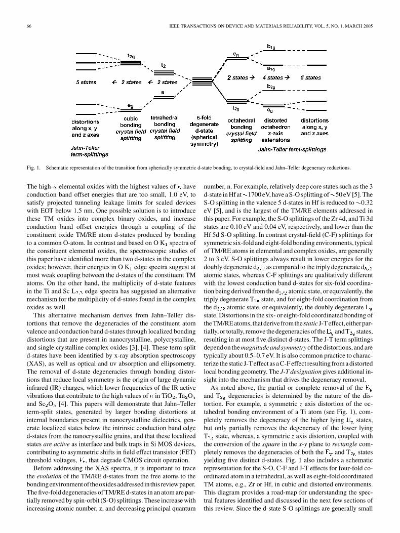
Fig. 1. Schematic representation of the transition from spherically symmetric d-state bonding, to crystal-field and Jahn–Teller degeneracy reductions.
The high- elemental oxides with the highest values of haveconduction band offset energies that are too small, 1.0 eV, tosatisfy projected tunneling leakage limits for scaled deviceswith EOT below 1.5 nm. One possible solution is to introducethese TM oxides into complex binary oxides, and increaseconduction band offset energies through a coupling of theconstituent oxide TM/RE atom d-states produced by bondingto a common O-atom. In contrast and based on O K spectra ofthe constituent elemental oxides, the spectroscopic studies ofthis paper have identified more than two d-states in the complexoxides; however, their energies in O K edge spectra suggest atmost weak coupling between the d-states of the constituent TMatoms. On the other hand, the multiplicity of d-state featuresin the Ti and Sc L edge spectra has suggested an alternativemechanism for the multiplicity of d-states found in the complexoxides as well.
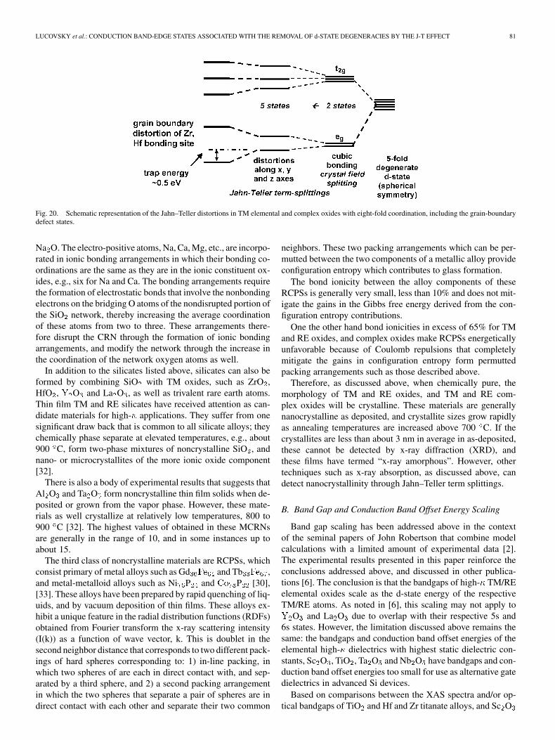
This alternative mechanism derives from Jahn–Teller dis-tortions that remove the degeneracies of the constituent atomvalence and conduction band d-states through localized bondingdistortions that are present in nanocrystalline, polycrystalline,and single crystalline complex oxides [3], [4]. These term-splitd-states have been identified by x-ray absorption spectroscopy(XAS), as well as optical and uv absorption and ellipsometry.The removal of d-state degeneracies through bonding distor-tions that reduce local symmetry is the origin of large dynamicinfrared (IR) charges, which lower frequencies of the IR activevibrations that contribute to the high values of in TiO , Ta Oand Sc O [4]. This papers will demonstrate that Jahn–Tellerterm-split states, generated by larger bonding distortions atinternal boundaries present in nanocrystalline dielectrics, gen-erate localized states below the intrinsic conduction band edged-states from the nanocrystallite grains, and that these localizedstates are active as interface and bulk traps in Si MOS devices,contributing to asymmetric shifts in field effect transistor (FET)threshold voltages, , that degrade CMOS circuit operation.
Before addressing the XAS spectra, it is important to tracethe evolution of the TM/RE d-states from the free atoms to thebondingenvironmentof theoxidesaddressedin this reviewpaper.The five-fold degeneracies of TM/RE d-states in an atom are par-tially removed by spin-orbit (S-O) splittings. These increase withincreasing atomic number, z, and decreasing principal quantum
number, n. For example, relatively deep core states such as the 3d-state in Hf at 1700 eV, have a S-O splitting of 50 eV [5]. TheS-O splitting in the valence 5 d-states in Hf is reduced to 0.32eV [5], and is the largest of the TM/RE elements addressed inthis paper. For example, the S-O splittings of the Zr 4d, and Ti 3dstates are 0.10 eV and 0.04 eV, respectively, and lower than theHf 5d S-O splitting. In contrast crystal-field (C-F) splittings forsymmetric six-fold and eight-fold bonding environments, typicalof TM/RE atoms in elemental and complex oxides, are generally2 to 3 eV. S-O splittings always result in lower energies for thedoubly degenerate d as compared to the triply degenerate datomic states, whereas C-F splittings are qualitatively differentwith the lowest conduction band d-states for six-fold coordina-tion being derived from the d atomic state, or equivalently, thetriply degenerate T state, and for eight-fold coordination fromthe d atomic state, or equivalently, the doubly degeneratestate. Distortions in the six- or eight-fold coordinated bonding oftheTM/REatoms, thatderive fromthestaticJ-Teffect, eitherpar-tially, or totally, remove the degeneracies of the and T states,resulting in at most five distinct d-states. The J-T term splittingsdepend on the magnitude and symmetry of the distortions, and aretypically about 0.5–0.7 eV. It is also common practice to charac-terize the static J-T effect as a C-F effect resulting from a distortedlocal bonding geometry. The J-T designation gives additional in-sight into the mechanism that drives the degeneracy removal.
As noted above, the partial or complete removal of theand T degeneracies is determined by the nature of the dis-tortion. For example, a symmetric z axis distortion of the oc-tahedral bonding environment of a Ti atom (see Fig. 1), com-pletely removes the degeneracy of the higher lying states,but only partially removes the degeneracy of the lower lyingT state, whereas, a symmetric z axis distortion, coupled withthe conversion of the square in the x-y plane to rectangle com-pletely removes the degeneracies of both the and T statesyielding five distinct d-states. Fig. 1 also includes a schematicrepresentation for the S-O, C-F and J-T effects for four-fold co-ordinated atom in a tetrahedral, as well as eight-fold coordinatedTM atoms, e.g., Zr or Hf, in cubic and distorted environments.This diagram provides a road-map for understanding the spec-tral features identified and discussed in the next few sections ofthis review. Since the d-state S-O splittings are generally small

LUCOVSKY et al.: CONDUCTION BAND-EDGE STATES ASSOCIATED WITH THE REMOVAL OF d-STATE DEGENERACIES BY THE J-T EFFECT 67
relative to the C-F splittings, and the changes in these due to J-Teffects, the S-O will be neglected in the discussions that follow.
II. EXPERIMENTAL PROCEDURES
XAS measurements were performed at the National Syn-chrotron Light Source (NSLS) at the Brookhaven NationalLaboratory (BNL), and at the Stanford Synchrotron RadiationLaboratories (SSRL) at the Stanford Linear Accelerator Center(SLAC) using total photo-electron yield to determine the rel-ative absorption strength of the spectral features associatedwith transitions from TM, RE, and O-atom core level states toempty conduction band-states [6]. Thin film samples of ZrOand HfO and their respective silicate alloys were prepared byremote plasma enhanced chemical vapor deposition (RPECVD)[7]. TiO and Hf Zr O TiO alloy thin films wereprepared by physical deposition of Ti and Hf(Zr) atoms, fol-lowed by in situ plasma-assisted oxidation, and by reactiveevaporation in an ultrahigh vacuum system in both instancesusing e-beam sources for the TM metals [8]. The growth ofGdScO and DyScO single crystals has been discussed in[9]. Thin films of LaAlO , and La Dy Gd O Sc O ,were also grown by reactive evaporation in an ultrahigh vacuumdeposition system using effusion cell sources for the TM andRE atoms [10].
III. X-RAY ABSORPTION SPECTROSCOPY STUDIES
OF TRANSITION METAL-OXIDE FILMS
A. Differences Between Intra- and Inter-Atomic Spectra
Fig. 2(a) and (b) presents Zr M and O K spectra for thinfilm nanocrystalline ZrO [6]. The Zr M spectrum in Fig. 2(a)is effectively an intra-atomic spectrum in which dipole-allowedtransitions from occupied Zr core level, spin-orbit split 3p-states( p and p ) terminate in empty Zr 4d and 5 s states that liewell above the top of the valence band edge, 5–6 eV. The en-ergy differences between: 1) the spectral peaks of two 3d-stateswith triply degenerate and doubly degenerate T character,
d d , and 2) the spectral peak of the first 3d-state and the4s-state d s are in good agreement ( 0.3 eV) with ab initocalculations based on small clusters with central Zr atoms, andtwo shells of atomic neighbors [11]. The relative intensities ofthe 4d- and 5s-features are markedly different, and are consis-tent with the contributions of the Zr atomic radial wave func-tions of the initial and final states to the transition matrix ele-ment [12]. The ab initio calculations also provide equally goodagreement with respect to the Zr-O bond length, and the spectralpeaks of features in the valence band spectrum as determined byUV photoemission spectroscopy [8], [11].
The ZrO O K spectrum in Fig. 2(b) is an inter-atomicatomic spectrum with final states reflecting a mixing of O p -and Zr d -, s - and p -states. Agreement with ab initiocalculations is approximately 0.3 eV as well [11].
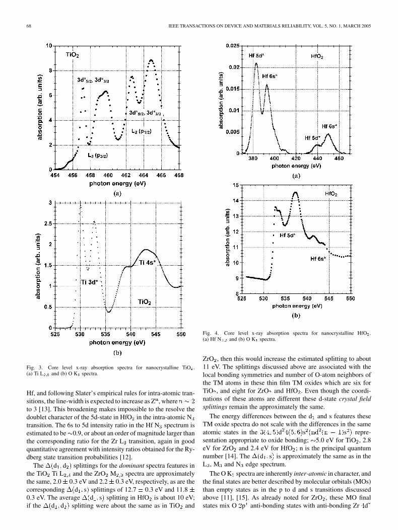
B. Intra- and Inter-Atomic Spectra for TiO , ZrO and HfO
Qualitatively similar spectra have been obtained for the corre-sponding TM p-state and O atom core level absorption spectrain TiO and HfO [6]. These include the Ti L and Hf N
Fig. 2. Core level x-ray absorption spectra for nanocrystalline ZrO .(a) Zr M spectra for excitation from spin-orbit split Zr 3p levels to empty Zr4d and 5s states, and (b) O K spectra for excitation from the O 1s level tomolecular orbital Zr 4d and 5s states mixed with O 2p states.
spectra, as well the respective TiO and HfO O K spectra. TheTi L and O K spectra for TiO are displayed in Fig. 3(a) and(b), and the Hf N and O K spectra for HfO are displayed inFig. 4(a) and (b). Differentiated O K spectra are displayed inFig. 5(a) and (b) for ZrO and HfO , respectively.
The relative intensities of features that terminate in empty d-and s-states, respectively, in Ti L , Zr M and Hf N spectraare consistent with the intra-atomic character of these transi-tions. This has been established by comparing the ratios of theintegrated absorption of the d-state and s-state features in therespective L , M , and N spectra with the transition probabil-ities for the corresponding Rydberg state transitions [12]. Forexample, this ratio is for 2p to 4s and 3dtransitions in TiO , and increases to for 5sto 4d transitions in ZrO [13]. The relative line-widths of the dfeatures increase markedly as the atomic number, Z, of the tran-sition metal atom increases. Z for Ti, 40 for Zr and 72 for
68 IEEE TRANSACTIONS ON DEVICE AND MATERIALS RELIABILITY, VOL. 5, NO. 1, MARCH 2005
Fig. 3. Core level x-ray absorption spectra for nanocrystalline TiO .(a) Ti L and (b) O K spectra.
Hf, and following Slater’s empirical rules for intra-atomic tran-sitions, the line-width is expected to increase as Z , whereto 3 [13]. This broadening makes impossible to the resolve thedoublet character of the 5d-state in HfO in the intra-atomic Ntransition. The 6s to 5d intensity ratio in the Hf N spectrum isestimated to be 0.9, or about an order of magnitude larger thanthe corresponding ratio for the Zr L transition, again in goodquantitative agreement with intensity ratios obtained for the Ry-dberg state transition probabilities [12].
The d d splittings for the dominant spectra features inthe TiO Ti L and the ZrO M spectra are approximatelythe same, 2.0 0.3 eV and 2.2 0.3 eV, respectively, as are thecorresponding d s splittings of 12.7 0.3 eV and 11.80.3 eV. The average d s splitting in HfO is about 10 eV;if the d d splitting were about the same as in TiO and
Fig. 4. Core level x-ray absorption spectra for nanocrystalline HfO .(a) Hf N and (b) O K spectra.
ZrO , then this would increase the estimated splitting to about11 eV. The splittings discussed above are associated with thelocal bonding symmetries and number of O-atom neighbors ofthe TM atoms in these thin film TM oxides which are six forTiO , and eight for ZrO and HfO . Even though the coordi-nations of these atoms are different these d-state crystal fieldsplittings remain the approximately the same.
The energy differences between the d and s features theseTM oxide spectra do not scale with the differences in the sameatomic states in the d s s repre-sentation appropriate to oxide bonding; 5.0 eV for TiO , 2.8eV for ZrO and 2.4 eV for HfO ; n is the principal quantumnumber [14]. The d s is approximately the same as in theL , M and N edge spectrum.
The O K spectra are inherently inter-atomic in character, andthe final states are better described by molecular orbitals (MOs)than empty states as in the p to d and s transitions discussedabove [11], [15]. As already noted for ZrO , these MO finalstates mix O p anti-bonding states with anti-bonding Zr d

LUCOVSKY et al.: CONDUCTION BAND-EDGE STATES ASSOCIATED WITH THE REMOVAL OF d-STATE DEGENERACIES BY THE J-T EFFECT 69
Fig. 5. Differentiated O K spectra for (a) ZrO and (b) HfO . The markersindicate the multiplicity of d -state features.
states, with transition matrix elements consistent with the sym-metries of the MO initial and final states. These transitions dis-play differences in the relative amplitudes of the doublet d fea-tures that are related to the six-fold coordination of Ti, and theeight-fold coordination of Zr and Hf. The T or d triply de-generate states contribute to the d feature in TiO , whereas the
or d doubly degenerate states contribute to the d featuresin ZrO and HfO . The d d splittings increase from 2.7
0.2 eV in TiO , to in 3.2 0.2 eV ZrO , and 4.3 0.2 eVin HfO , while the d s splitting is 8, 4 0.2 eV in TiO ,and approximately the same in ZrO and HfO , 10.1 0.2 eVand 9.6 0.2 eV, respectively.
Equally importantly, the differences in photon energy be-tween the first d -state spectral peaks in the spectra ofTiO at 530.1 0.2 eV, ZrO at 532.2 0.2 eV, and HfO at532. eV, respectively, are the same to within an experimentaluncertainty of 0.3 eV as the differences in the experimentally
Fig. 6. Expanded x axis plot of the L component of the L spectrum ofnanocrystalline TiO .
determined optical bandgaps, , 3.1 eV for TiO eVfor ZrO , and 5.8 eV for HfO [1], [2], [6], [15].
The correlation between the energies of the d features inthe O K spectra of TiO , ZrO and HfO and the energies ofthe atomic d-states for the electronic configuration appropriateto oxides, s , where 3, 4 and 5, respectivelyfor Ti, Zr and Hf [6], [14], has important implications for thescaling of these optical bandgaps, , and conduction bandoffset energies with respect to Si, defined here as . This willbe addressed in Section III-D. It is equally important to corre-late features XAS spectra with photoconductivity (PC), internalphotoemission (IPE) [16], and band edge dielectric functionsand absorption obtained from spectroscopic ellipsometry (SE)studies, and this will be addressed later in this paper for bothelemental and complex oxides.
C. Intra- and Inter-Atomic Spectra for TiO , ZrO and HfO
Fig. 6 displays an expanded view of the L spectrum of TiO .Combined with Fig. 5(a) and (b) which display differentiatedspectra of the O K edge spectra of ZrO in Fig. 5(a) and HfOin Fig. 5(b), these three spectra clearly indicate a multiplicityof five for the d-state features which is greater than what is ex-pected from the local bonding symmetry crystal field splittingwhich predicts two features corresponding to one doubly degen-erate and one triply degenerate state. To better understand the in-creased d-state multiplicity, the evolution the removal of d-statedegeneracies with changes in the local bonding environmentsof the TM atoms in TM oxides has been presented in Fig. 1.This approach will also be useful in understanding the spectraof more complex oxides, comprised of TM oxides in combina-tion with: 1) other TM oxides as in HfZiO ; 2) lanthanide seriesrare earth (RE) oxides as in GdScO ; and 3) nontransition metaloxides as LaAlO .
There are no symmetry driven splittings of TM/RE d-statesin a spherically symmetric environment of nearest neighboroxygen atoms, e.g., for a coordination number of twelve as in

70 IEEE TRANSACTIONS ON DEVICE AND MATERIALS RELIABILITY, VOL. 5, NO. 1, MARCH 2005
Fig. 7. O K edge and differentiated O K spectra for a noncrystallineZr silicate alloy with �60 molecular percent ZrO : (ZrO ) (SiO ) .The dashed line markers indicate the positions of the spectral features innanocrystalline ZrO2 thin films.
perovskite structure [4]. Stated differently the doubly degen-erate d and triply degenerate d states are at the sameenergy giving rise to a d-state that is five fold degenerate. Thisdegeneracy is removed in octahedral, tetragonal and cubicbonding environments as indicated in the diagram. The removalof this d-state degeneracy is generally designated as a crystalfield splitting, and has been described at length in texts thathave addressed TM/RE molecules and crystalline solids [3],[4], [15]. Other bonding environments with lower symmetry,such as the bonding of a TM atom at the center of a square alsoremove the degeneracies of the d and d states as well[15].
Crystal field splittings of the type described above areobserved in noncrystalline Zr and Hf silicate alloys, and arepresentative O K edge spectrum for a Zr silicate alloy
ZrO is presented in Fig. 7. There is no evidencein the absorption spectrum, or the derivative of the absorptionspectrum of this representative silicate alloy for any additionald-state multiplicity indicative of a further removal of d-statedegeneracy. The O K spectrum (not shown) of this Zr silicatealloy indicates are reduction of the 4d-state line-width after ananneal at 900 C which results in chemical phase separationinto crystalline ZrO and noncrystalline SiO [7].
In marked contrast are the spectra in Figs. 6 and 5(a) and (b).Fig. 6 indicates the L edge spectrum of TiO in which five fea-tures are clearly evident. The number of distinct features in con-sistent with the complete removal of the d and d degenera-cies. The lower energy T triplet displays approximately equalsplittings of 0.75 0.5 eV between these three states, and thehigher energy doublet has an approximate splitting of 0.80.2 eV. These term-splittings are consistent with the distortedoctahedral bonding environment of Ti in crystalline TiO witha rutile structure [3], [4], [11]. The octahedral arrangement ofO atoms about the Ti atom displays a symmetric Ti-O bondingelongation of about 0.003 nm in the z-direction; the bonds in
the x-y plane are the same length, but the square arrangementof an ideal octahedron in this plane is converted to a rectangleby an approximately seven degre (7 ) bond angle change [11].These degeneracy removals are commonly referred to as staticJahn–Teller term splittings, since the distortion increases thebinding energy. This is contrast to dynamic Jahn–Teller split-tings that occur during optical or near UV excitation [3], [15].The increased bonding energy comes about because the numberof d-electrons is two, and these occupy a lower energy state afterthe symmetric T term splitting. These term splittings are notevident in the TiO O K edge spectrum of TiO , nor in the dif-ferentiation of the that spectrum as well, but as will discussedlater on in this paper are clearly evident in both the photoconduc-tivity response and in the dielectric constant and absorption con-stant extracted from spectroscopic ellipsometry measurements.
It is important to note that in nonmolecular solids, these termsplittings can only occur in a crystalline environment becausethey require symmetry reductions that involve second neighborsas well. The Jahn–Teller term splittings can also be viewed asa special class of crystal field effects; however, this nomencla-ture does not provide an insight into the forces that contribute tothe distorted bonding environment; i.e., an increase in bindingenergy associated with occupancy of the lowest term split state.The evolution of symmetry reductions that result from distor-tions of octahedral, as well as cubic and tetrahedral bonding inthe context of the Jahn–Teller effect are displayed in Fig. 1, andinclude the octahedral and cubic distortions important for: 1) Tiand Sc, and 2) Zr and Hf, respectively.
In marked contrast to the results described above for TiO ,the O K derivative spectra in Fig. 5(a) and (b) indicate a com-plete removal of d-state degeneracies in nanocrystalline ZrOand HfO , respectively. These degeneracy removals are not ev-ident in the Zr M and Hf N spectra, consistent with a signifi-cantly longer core hole life-time associated with the O 1s statethan for the Zr 3p and Hf 4p states. Core hole life-times scaleinversely as the atomic number, Z , of the atom from which theexcitation occurs, where –3.
Returning to the differentiated spectra in Fig. 5(a) and (b), thelower energy components of the d -state spectral features aresplit into two states and the higher frequency components intothree states. This is consistent with the Jahn–Teller term split-tings in cubic bonding environments in which there are distor-tions along all three principal axes. For distorted cubic bonding,the doublet or d state is lower in energy than the tripletT or d state, or exactly the reverse of the ordering in anoctahedral environment with distortions along the three coordi-nate axes. The d-state splittings for HfO are approximately 1.2to 1.3 eV and larger by about 50% compared to those for TiO ,providing a partial explanation for their observabilities in theO K edge spectra.
Fig. 8 indicates the Jahn–Teller term splittings for ZrO andHfO spectral features in the O K edge. This figure also in-cludes the TiO spectral features. For TiO , the highest energystate of the T triplet in the Ti L spectrum has been set equalto the lower energy d feature in the O K spectrum. This ap-proach is consistent with the spectra of Zr titanate alloys to bediscussed in the next section of this paper. Finally, the averaged -state energies obtained from this analysis of the respective

LUCOVSKY et al.: CONDUCTION BAND-EDGE STATES ASSOCIATED WITH THE REMOVAL OF d-STATE DEGENERACIES BY THE J-T EFFECT 71
Fig. 8. Jahn–Teller term splittings for the ZrO and HfO spectral features inthe O K edge. This figure also includes the TiO spectral features that havebeen scaled from the L edge spectrum by equating the energies of the twostrongest features in the TiO O K and L spectra. The diagram also includesthe average energies, E , of the respective d-state features.
O K spectra scale monotonically with the atomic d-state ener-gies of the atomic species, Ti, Zr, and Hf.
D. Band Gap and Conduction Band Offset Energy Scaling inElemental Oxides: The Motivation for Studying Band EdgeStates in Complex Oxides
Robertson has developed a charge neutrality level (CNL)model for determination of conduction band offset energies forhigh- dielectrics formed on Si [2]. The results presented in [2]are plotted in this paper in Fig. 9 to reveal an approximatelylinear relationship for as a function of . Fig. 9(a)and (b) contains plots, respectively, of: 1) as a functionof , and 2) and as a functions of atomic d stateenergy for a representative set of TM oxides. The scalingin Fig. 9(b) follows directly from the spectroscopic resultspresented above, and from the ab initio calculations for O Kspectra that provide the correlation between optical bandgapsand atomic d-state energies [11]. A band offset energy of atleast 1 eV, and more generally about 1.2 eV or more is requiredfor tunneling/thermionic leakage current to be sufficiently lowfor scaled CMOS devices [17]. Using this criterion, the TMoxides with the highest dielectric constants, TiO , and Nb Oand Ta O , have offset energies below 1 eV that either corre-late with high tunneling leakage, and/or electric field assistedinjection into low-lying conduction band-states associated withthese atoms, and are therefore not candidates for replacementdielectrics in scaled CMOS devices. Based on this scaling withatomic d-states, the elemental oxides of: 1) Zr and Hf and 2)Y, La and the lanthanide RE oxides are expected to have con-duction band offset energies 1.2 eV, and therefore have thepotential for meeting roadmap targets for low tunneling leakagecurrent, provided that the electron tunneling mass, , doesnot decrease significantly with decreasing , and mitigategains for increases in [see (1)]. Since the TM and RE d-statesdo not mix with the lowest conduction band s-states of Si andAl, these scaling arguments can be extended to the silicate
Fig. 9. (a) Conduction band offset energy, E , as a function of the opticalbandgap, E , from the results presented in [2]. (b) E and E as a function ofatomic d-state energy.
and aluminate alloys of the Zr, Hf, Y, La and the lanthanideRE atoms [7]. However, it must be recognized that there aremany other factors that contribute to the integration of high-dielectrics into advanced Si devices [1]. These include processintegration issues relative to thermal budgets, substitution ofdual metal or single midgap metal gates for bulk and thin filmSi on insulator devices, respectively, as well as other high-dielectric issues including: 1) internal dielectric interfaces withultrathin interfacial SiO layers [18], [19], and 2) intrinsic bandedge traps addressed in this paper [20], [21].
The results presented above have raised an interesting ques-tion regarding the lowest energy d -states in complex oxidesthat include Sc and Ti, as for example stoichiometric and Zr andHf titanates, and RE scandates such as La, Dy and Gd scandate:is it possible for d-states of the two TM atoms in the titanates,and the Sc and RE atoms of the scandates to couple and mix inways that increase the optical bandgap, and the conduction bandoffset energies of these complex alloys? If this mixing were tooccur this would then provide a way to obtain independent con-trol of band offset energies and dielectric constants, and thereby
72 IEEE TRANSACTIONS ON DEVICE AND MATERIALS RELIABILITY, VOL. 5, NO. 1, MARCH 2005
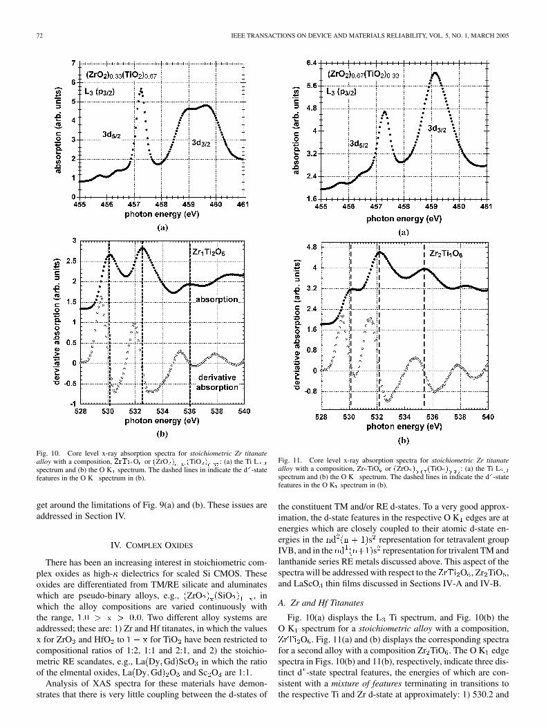
Fig. 10. Core level x-ray absorption spectra for stoichiometric Zr titanatealloy with a composition, ZrTi O or (ZrO ) (TiO ) : (a) the Ti Lspectrum and (b) the O K spectrum. The dashed lines in indicate the d -statefeatures in the O K spectrum in (b).
get around the limitations of Fig. 9(a) and (b). These issues areaddressed in Section IV.
IV. COMPLEX OXIDES
There has been an increasing interest in stoichiometric com-plex oxides as high- dielectrics for scaled Si CMOS. Theseoxides are differentiated from TM/RE silicate and aluminateswhich are pseudo-binary alloys, e.g., ZrO SiO , inwhich the alloy compositions are varied continuously withthe range, . Two different alloy systems areaddressed; these are: 1) Zr and Hf titanates, in which the valuesx for ZrO and HfO to for TiO have been restricted tocompositional ratios of 1:2, 1:1 and 2:1, and 2) the stoichio-metric RE scandates, e.g., La Dy Gd ScO in which the ratioof the elmental oxides, La Dy Gd O and Sc O are 1:1.
Analysis of XAS spectra for these materials have demon-strates that there is very little coupling between the d-states of
Fig. 11. Core level x-ray absorption spectra for stoichiometric Zr titanatealloy with a composition, Zr TiO or (ZrO ) (TiO ) : (a) the Ti Lspectrum and (b) the O K spectrum. The dashed lines in indicate the d -statefeatures in the O K spectrum in (b).
the constituent TM and/or RE d-states. To a very good approx-imation, the d-state features in the respective O K edges are atenergies which are closely coupled to their atomic d-state en-ergies in the s representation for tetravalent groupIVB, and in the s representation for trivalent TM andlanthanide series RE metals discussed above. This aspect of thespectra will be addressed with respect to the O , Zr TiO ,and LaScO thin films discussed in Sections IV-A and IV-B.
A. Zr and Hf Titanates
Fig. 10(a) displays the L Ti spectrum, and Fig. 10(b) theO K spectrum for a stoichiometric alloy with a composition,
O . Fig. 11(a) and (b) displays the corresponding spectrafor a second alloy with a composition Zr TiO . The O K edgespectra in Figs. 10(b) and 11(b), respectively, indicate three dis-tinct d -state spectral features, the energies of which are con-sistent with a mixture of features terminating in transitions tothe respective Ti and Zr d-state at approximately: 1) 530.2 and

LUCOVSKY et al.: CONDUCTION BAND-EDGE STATES ASSOCIATED WITH THE REMOVAL OF d-STATE DEGENERACIES BY THE J-T EFFECT 73
532.4 eV for TiO and 2) 532.4 and 535.4 to 536.0 eV for ZrO ,each with an experimental uncertainty of 0.1 eV. This meansthat the lowest energy spectral feature is TiO -like, the highestspectral feature ZrO -like, and the middle frequency has con-tributions from both TiO and ZrO . Derivative O K spectrado not indicate and additional d -state spectral features. The re-spective Ti L spectra in Figs. 10(a) and 11(a), provide evidencefor Jahn–Teller term splittings indicating a complete removal ofthe Ti 3d state degeneracies. The presence of the term split fea-tures in the Ti L spectra, and their absence in the respectiveO K edge spectra is essentially the same behavior noted abovefor TiO O K and Ti L spectra. The T term-split energiesof the three lower -states in the Ti L spectra are the same foreach composition, whereas there are marked differences in thetwo term-splitting of the -states. These are consistent withdifferences in the character of the bonding between Ti and itssecond neighbors: 1) a mixture of ionic and covalent bondingfor a compositionally averaged mixture of Zr and Ti neighborsfor O , and 2) a more ionic bonding with a compositionalaverage two Zr neighbors in Zr TiO [3]. The second neighborbonding has little effect on the T -bonding states which arelocalized on the nearest neighbor Ti and O, but has a strong in-fluence on the -bonding states which are significantly moredelocalized.
The O K spectra of Hf titanate alloys, HfO SiO ,with: 1) , , , , and and
display qualitatively and quantitative similar spectra tothe Zr titanates discussed above. To a good approximation, thefeatures in the O K edge are also well described by a mixtureof HfO and TiO features, with small shifts that are consistentwith a weak coupling between Ti and Hf d-states with the samesymmetries. This is illustrated in Fig. 12(a) and (b) for HfTiO ,or the 1:1 composition: HfO SiO . The TM -states thatform the top of the valence band and the bottom of conduc-tion band are predominantly Ti-like and are shifted by less than0.5 eV from their values in the TiO , whereas there are largershifts, 1 eV in the Hf-like -bond states that are at the bottomof the valence band higher in the conduction band. One expla-nation proposed for this behavior was that it was indicative ofrelatively weak coupling between the -bonded states that areat the top of valence band, and stronger coupling between the
-bonded states that are deeper in the valence band [8]. How-ever, this explanation fails to take into account the strong con-tribution of O 2p nonbonding states at the top of the valenceband [6]. On the other hand, the differences in the valence bandstates of the elemental and complex oxides are explained quan-titatively by noting that the valence and conduction band spectraof the constituent elemental oxides, TiO and HfO include theeffects of Jahn–Teller term splittings, whereas those of the com-plex oxide, HfTiO include Jahn–Teller shifts for the Ti-atoms,but not the Hf-atoms. The 1 eV shifts of the states at the bottomof the valence band, and above the conduction band edge as re-vealed in the O K spectrum. The smaller shifts in the states atthe top of valence band and bottom of the conduction band mayindeed be due to a weak coupling of -bonded states; however,this will require additional study.
Similar valence band, and O K edge shifts have been foundin Zr titanate alloys, and additional compositions are being
Fig. 12. (a) O K and (b) UPS valence band spectra for HfTiO , orequivalently an Hf titante alloy with 1:1 composition of HfO and TiO . Thearrows in (a) and (b) indicate the smaller shifts in the �-bonded states at the topof the valence band and bottom of the conduction, as well as the larger shifts inthe �-bonded states at the bottom of the valence band and at higher energies inthe conduction band.
studied to see if the observed shifts correlate with Zr titanatephases, or mixtures of ZrO and HfO . Stated otherwise,comparisons between Zr titanate alloys and the end-memberoxides may prove to be a novel way of identifying compo-sitions that correspond to stoichiometric complex oxides, asdistinguished from alloys with random, or statistical bondingof the constituent elemental oxides.
B. La and Other RE Scandates
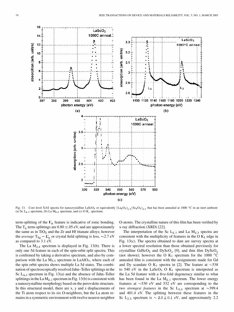
Qualitatively similar behavior are presented for stoichio-metric La, Dy, and Gd scandates. Sc L , La M and O Kspectra are presented in Fig. 13(a), (b), and (c), respectively,for LaScO or equivalently La O Sc O that has beenannealed at 1000 C in an inert ambient. The Sc L spectrumin Fig. 13(a) displays a Jahn–Teller term-splitting similar tothose of the Ti spectrum for Zr TiO in Fig. 11(a), where the
74 IEEE TRANSACTIONS ON DEVICE AND MATERIALS RELIABILITY, VOL. 5, NO. 1, MARCH 2005
Fig. 13. Core level XAS spectra for nanocrystalline LaScO or equivalently (La O ) (Sc O ) that has been annealed at 1000 C in an inert ambient:(a) Sc L spectrum, (b) La M spectrum, and (c) O K spectrum.
term-splitting of the feature is indicative of ionic bonding.The T term-splittings are 0.80 .05 eV, and are approximatelythe same as in TiO and the Zr and Hf titanate alloys; howeverthe average T or crystal field splitting is less, 2.7 eVas compared to 3.1 eV.
The La M spectrum is displayed in Fig. 13(b). There isonly one 5d feature in each of the spin-orbit split spectra. Thisis confirmed by taking a derivative spectrum, and also by com-parison with the La M spectrum in LaAlO , where each ofthe spin orbit spectra shows multiple La 5d states. The combi-nation of spectroscopically resolved Jahn–Teller splittings in theSc L spectrum in Fig. 13(a) and the absence of Jahn–Tellersplittings in the La M spectrum in Fig. 13(b) is consistent witha nanocrystalline morphology based on the perovskite structure.In this structural model, there are x, y and z displacements ofthe Ti atom respect to its six O-neighbors, but the La atom re-mains in a symmetric environment with twelve nearest-neighbor
O-atoms. The crystalline nature of this film has been verified byx-ray diffraction (XRD) [22].
The interpretation of the Sc L and La M spectra areconsistent with the multiplicity of features in the O K edge inFig. 13(c). The spectra obtained to date are survey spectra ata lower spectral resolution than those obtained previously forcrystalline GdScO and DyScO [9], and thin film DyScO(not shown); however the O K spectrum for the 1000 Cannealed film is consistent with the assignments made for Gdand Dy scandate O K spectra in [2]. The feature at 538to 540 eV in the LaScO O K spectrum is interpreted asthe La 5d feature with a five-fold degeneracy similar to whathas been found in the La M spectrum. The lower energyfeatures at 530 eV and 532 eV are corresponding to thetwo strongest features in the Sc L spectrum at 399.4and 401.4 eV. The splitting between these features in theSc L spectrum is eV, and approximately 2.2
LUCOVSKY et al.: CONDUCTION BAND-EDGE STATES ASSOCIATED WITH THE REMOVAL OF d-STATE DEGENERACIES BY THE J-T EFFECT 75
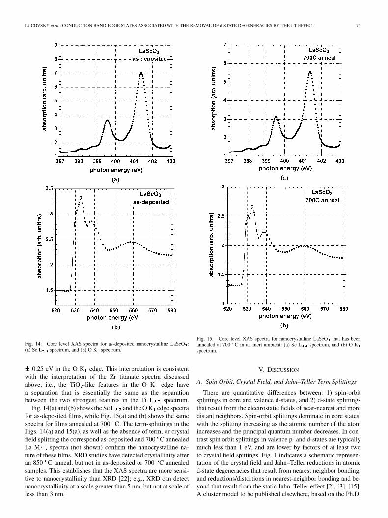
Fig. 14. Core level XAS spectra for as-deposited nanocrystalline LaScO :(a) Sc L spectrum, and (b) O K spectrum.
0.25 eV in the O K edge. This interpretation is consistentwith the interpretation of the Zr titanate spectra discussedabove; i.e., the TiO -like features in the O K edge havea separation that is essentially the same as the separationbetween the two strongest features in the Ti L spectrum.
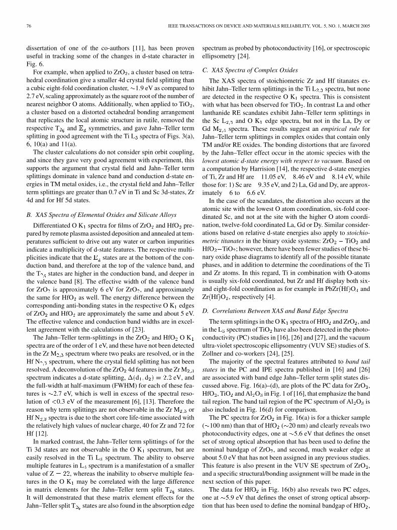
Fig. 14(a) and (b) shows the Sc L and the O K edge spectrafor as-deposited films, while Fig. 15(a) and (b) shows the samespectra for films annealed at 700 C. The term-splittings in theFigs. 14(a) and 15(a), as well as the absence of term, or crystalfield splitting the correspond as-deposited and 700 C annealedLa M spectra (not shown) confirm the nanocrystalline na-ture of these films. XRD studies have detected crystallinity afteran 850 C anneal, but not in as-deposited or 700 C annealedsamples. This establishes that the XAS spectra are more sensi-tive to nanocrystallinity than XRD [22]; e.g., XRD can detectnanocrystallinity at a scale greater than 5 nm, but not at scale ofless than 3 nm.
Fig. 15. Core level XAS spectra for nanocrystalline LaScO that has beenannealed at 700 C in an inert ambient: (a) Sc L spectrum, and (b) O Kspectrum.
V. DISCUSSION
A. Spin Orbit, Crystal Field, and Jahn–Teller Term Splittings
There are quantitative differences between: 1) spin-orbitsplittings in core and valence d-states, and 2) d-state splittingsthat result from the electrostatic fields of near-nearest and moredistant neighbors. Spin-orbit splittings dominate in core states,with the splitting increasing as the atomic number of the atomincreases and the principal quantum number decreases. In con-trast spin orbit splittings in valence p- and d-states are typicallymuch less than 1 eV, and are lower by factors of at least twoto crystal field spittings. Fig. 1 indicates a schematic represen-tation of the crystal field and Jahn–Teller reductions in atomicd-state degeneracies that result from nearest neighbor bonding,and reductions/distortions in nearest-neighbor bonding and be-yond that result from the static Jahn–Teller effect [2], [3], [15].A cluster model to be published elsewhere, based on the Ph.D.
76 IEEE TRANSACTIONS ON DEVICE AND MATERIALS RELIABILITY, VOL. 5, NO. 1, MARCH 2005
dissertation of one of the co-authors [11], has been provenuseful in tracking some of the changes in d-state character inFig. 6.
For example, when applied to ZrO , a cluster based on tetra-hedral coordination give a smaller 4d crystal field splitting thana cubic eight-fold coordination cluster, 1.9 eV as compared to2.7 eV, scaling approximately as the square root of the number ofnearest neighbor O atoms. Additionally, when applied to TiO ,a cluster based on a distorted octahedral bonding arrangementthat replicates the local atomic structure in rutile, removed therespective T and symmetries, and gave Jahn–Teller termsplitting in good agreement with the Ti L spectra of Figs. 3(a),6, 10(a) and 11(a).
The cluster calculations do not consider spin orbit coupling,and since they gave very good agreement with experiment, thissupports the argument that crystal field and Jahn–Teller termsplittings dominate in valence band and conduction d-state en-ergies in TM metal oxides, i.e., the crystal field and Jahn–Tellerterm splittings are greater than 0.7 eV in Ti and Sc 3d-states, Zr4d and for Hf 5d states.
B. XAS Spectra of Elemental Oxides and Silicate Alloys
Differentiated O K spectra for films of ZrO and HfO pre-pared by remote plasma assisted deposition and annealed at tem-peratures sufficient to drive out any water or carbon impuritiesindicate a multiplicity of d-state features. The respective multi-plicities indicate that the states are at the bottom of the con-duction band, and therefore at the top of the valence band, andthe T states are higher in the conduction band, and deeper inthe valence band [8]. The effective width of the valence bandfor ZrO is approximately 6 eV for ZrO , and approximatelythe same for HfO as well. The energy difference between thecorresponding anti-bonding states in the respective O K edgesof ZrO and HfO are approximately the same and about 5 eV.The effective valence and conduction band widths are in excel-lent agreement with the calculations of [23].
The Jahn–Teller term-splittings in the ZrO and HfO O Kspectra are of the order of 1 eV, and these have not been detectedin the Zr M spectrum where two peaks are resolved, or in theHf N spectrum, where the crystal field splitting has not beenresolved. A deconvolution of the ZrO 4d features in the Zr Mspectrum indicates a d-state splitting, d d eV, andthe full-width at half-maximum (FWHM) for each of these fea-tures is 2.7 eV, which is well in excess of the spectral reso-lution of 0.3 eV of the measurement [6], [13]. Therefore thereason why term splittings are not observable in the Zr M orHf N spectra is due to the short core life-time associated withthe relatively high values of nuclear charge, 40 for Zr and 72 forHf [12].
In marked contrast, the Jahn–Teller term splittings of for theTi 3d states are not observable in the O K spectrum, but areeasily resolved in the Ti L spectrum. The ability to observemultiple features in L spectrum is a manifestation of a smallervalue of Z , whereas the inability to observe multiple fea-tures in the O K may be correlated with the large differencein matrix elements for the Jahn–Teller term split T states.It will demonstrated that these matrix element effects for theJahn–Teller split T states are also found in the absorption edge
spectrum as probed by photoconductivity [16], or spectroscopicellipsometry [24].
C. XAS Spectra of Complex Oxides
The XAS spectra of stoichiometric Zr and Hf titanates ex-hibit Jahn–Teller term splittings in the Ti L spectra, but noneare detected in the respective O K spectra. This is consistentwith what has been observed for TiO . In contrast La and otherlanthanide RE scandates exhibit Jahn–Teller term splittings inthe Sc L and O K edge spectra, but not in the La, Dy orGd M spectra. These results suggest an empirical rule forJahn–Teller term splittings in complex oxides that contain onlyTM and/or RE oxides. The bonding distortions that are favoredby the Jahn–Teller effect occur in the atomic species with thelowest atomic d-state energy with respect to vacuum. Based ona computation by Harrision [14], the respective d-state energiesof Ti, Zr and Hf are 11.05 eV, 8.46 eV and 8.14 eV, whilethose for: 1) Sc are 9.35 eV, and 2) La, Gd and Dy, are approx-imately 6 to 6.6 eV.
In the case of the scandates, the distortion also occurs at theatomic site with the lowest O atom coordination, six-fold coor-dinated Sc, and not at the site with the higher O atom coordi-nation, twelve-fold coordinated La, Gd or Dy. Similar consider-ations based on relative d-state energies also apply to stoichio-metric titanates in the binary oxide systems: ZrO TiO andHfO TiO ; however, there have been fewer studies of these bi-nary oxide phase diagrams to identify all of the possible titanatephases, and in addition to determine the coordinations of the Tiand Zr atoms. In this regard, Ti in combination with O-atomsis usually six-fold coordinated, but Zr and Hf display both six-and eight-fold coordination as for example in PbZr Hf O andZr Hf O , respectively [4].
D. Correlations Between XAS and Band Edge Spectra
The term splittings in the O K spectra of HfO and ZrO , andin the L spectrum of TiO have also been detected in the photo-conductivity (PC) studies in [16], [26] and [27], and the vacuumultra-violet spectroscopic ellipsomentry (VUV SE) studies of S.Zollner and co-workers [24], [25].
The majority of the spectral features attributed to band tailstates in the PC and IPE spectra published in [16] and [26]are associated with band edge Jahn–Teller term split states dis-cussed above. Fig. 16(a)–(d), are plots of the PC data for ZrO ,HfO , TiO and Al O in Fig. 1 of [16], that emphasize the bandtail region. The band tail region of the PC spectrum of Al O isalso included in Fig. 16(d) for comparison.
The PC spectra for ZrO in Fig. 16(a) is for a thicker sample( 100 nm) than that of HfO ( 20 nm) and clearly reveals twophotoconductivity edges, one at 5.6 eV that defines the onsetset of strong optical absorption that has been used to define thenominal bandgap of ZrO , and second, much weaker edge atabout 5.0 eV that has not been assigned in any previous studies.This feature is also present in the VUV SE spectrum of ZrO ,and a specific structural/bonding assignment will be made in thenext section of this paper.
The data for HfO in Fig. 16(b) also reveals two PC edges,one at 5.9 eV that defines the onset of strong optical absorp-tion that has been used to define the nominal bandgap of HfO ,
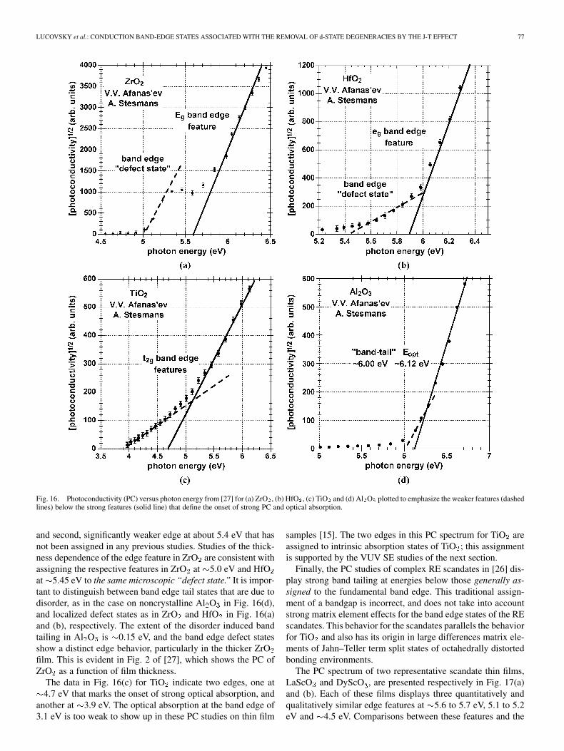
LUCOVSKY et al.: CONDUCTION BAND-EDGE STATES ASSOCIATED WITH THE REMOVAL OF d-STATE DEGENERACIES BY THE J-T EFFECT 77
Fig. 16. Photoconductivity (PC) versus photon energy from [27] for (a) ZrO , (b) HfO , (c) TiO and (d) Al O plotted to emphasize the weaker features (dashedlines) below the strong features (solid line) that define the onset of strong PC and optical absorption.
and second, significantly weaker edge at about 5.4 eV that hasnot been assigned in any previous studies. Studies of the thick-ness dependence of the edge feature in ZrO are consistent withassigning the respective features in ZrO at 5.0 eV and HfOat 5.45 eV to the same microscopic “defect state.” It is impor-tant to distinguish between band edge tail states that are due todisorder, as in the case on noncrystalline Al O in Fig. 16(d),and localized defect states as in ZrO and HfO in Fig. 16(a)and (b), respectively. The extent of the disorder induced bandtailing in Al O is 0.15 eV, and the band edge defect statesshow a distinct edge behavior, particularly in the thicker ZrOfilm. This is evident in Fig. 2 of [27], which shows the PC ofZrO as a function of film thickness.
The data in Fig. 16(c) for TiO indicate two edges, one at4.7 eV that marks the onset of strong optical absorption, and
another at 3.9 eV. The optical absorption at the band edge of3.1 eV is too weak to show up in these PC studies on thin film
samples [15]. The two edges in this PC spectrum for TiO areassigned to intrinsic absorption states of TiO ; this assignmentis supported by the VUV SE studies of the next section.
Finally, the PC studies of complex RE scandates in [26] dis-play strong band tailing at energies below those generally as-signed to the fundamental band edge. This traditional assign-ment of a bandgap is incorrect, and does not take into accountstrong matrix element effects for the band edge states of the REscandates. This behavior for the scandates parallels the behaviorfor TiO and also has its origin in large differences matrix ele-ments of Jahn–Teller term split states of octahedrally distortedbonding environments.
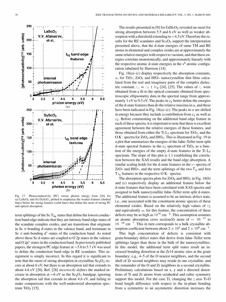
The PC spectrum of two representative scandate thin films,LaScO and DyScO , are presented respectively in Fig. 17(a)and (b). Each of these films displays three quantitatively andqualitatively similar edge features at 5.6 to 5.7 eV, 5.1 to 5.2eV and 4.5 eV. Comparisons between these features and the
78 IEEE TRANSACTIONS ON DEVICE AND MATERIALS RELIABILITY, VOL. 5, NO. 1, MARCH 2005
Fig. 17. Photoconductivity (PC) versus photon energy from [26] for(a) LaScO and (b) DyScO plotted to emphasize the weaker features (dashedlines) below the strong features (solid lines) that define the onset of strong PCand optical absorption.
term splittings of the Sc T states that define the lowest conduc-tion band edge indicate that they are intrinsic band edge states ofthe scandate complex oxides, and are transitions that originatein Sc -bonding d-states in the valence band, and terminate inSc -anti-bonding d -states of the conduction band. As notedabove these Sc d-states are coupled to O 2p states in the valenceand O p states in the conduction band. In previously publishedpapers, the strongest PC edge feature at 5.6 to 5.7 eV was usedto define the conduction band edge in RE scandates. This as-signment is simply incorrect. In this regard it is significant tonote that the onset of strong absorption in crystalline Sc O oc-curs at about 6 eV, but there is an absorption tail that extends toabout 4.6 eV [28]. Ref. [28] incorrectly defines the marked in-crease in absorption at 6 eV as the Sc O bandgap, ignoringthe absorption tail that extends to about 4.6 eV, and failing tomake comparisons with the well-understood absorption spec-trum TiO [15].
The results presented in [9] for GdScO revealed an onset forstrong absorption between 5.5 and 6 eV as well as weaker ab-sorption with a threshold extending to 4.5 eV. Therefore the re-sults for the RE scandates and Sc O support the interpretationpresented above, that the d-state energies of same TM and REatoms in elemental and complex oxides are at approximately thesame relative energies with respect to vacuum, and that these en-ergies correlate monotonically, and approximately linearly withthe respective atomic d-state energies in the s atomic configu-ration tabulated by Harrison [14].
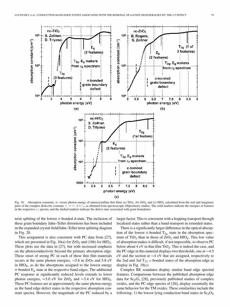
Fig. 18(a)–(c) display respectively the absorption constants,, for TiO , ZrO and HfO nanocrystalline thin films calcu-
lated from the real and imaginary parts of the complex dielec-tric constant, [24], [25]. The values of wereobtained from a fit to the optical constants obtained from spec-troscopic ellipsometry data in the spectral range from approxi-mately 1 eV to 9.5 eV. The peaks in better define the energiesof the d-state features than do the relative maxima in , and thesehave been indicated in Fig. 18(a)–(c). The peaks in are shiftedin energy because they include a contribution from as well as
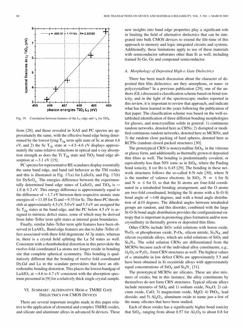
. Before commenting on the additional band edge feature ineach of these spectra, it is important to note that there is excellentagreement between the relative energies of these features, andthose obtained from either the Ti L spectrum for TiO , and theO K spectra for ZrO and HfO . This is illustrated in Fig. 19 ina plot that summarizes the energies of the Jahn–Teller term splitd-state spectral features in the spectrum of TiO as a func-tion of the energies of the empty d-state features in the Ti Lspectrum. The slope of this plot is 1.1 establishing the correla-tion between the XAS results and the band edge absorption. Asimilar scaling holds for the d-state features in the spectra ofZrO and HfO , and the term splittings of the two and firstT features in the respective O K spectra.
The absorption spectra plots for ZrO and HfO in Fig. 18(b)and (c) respectively display an additional feature below thed-state features that have been correlated with XAS spectra andassigned to bulk nanocrystallite Jahn–Teller term split d-states.The additional feature is assumed to be an intrinsic defect state,i.e., one associated with the constituent atomic species of theseelemental oxides. Based on the relatively high values ofand equivalently , for this feature, the concentration of thesedefects may be as high as cm . This assumption assumesan atomic absorption cross section/Zr atom of to
cm . This in turn corresponds to a bulk crystallite ab-sorption coefficient between about and cm .
This high concentration of defects is consistent withgrain-boundary defect states that derive from Jahn–Teller termsplittings larger than those in the bulk of the nanocrystallites.In this model, the additional term split states result an in-creased bonding distortion at the Zr14 atomic sites at the grainboundary; e.g., 4–5 of the O nearest neighbors, and the secondshell of Zr second neighbors may reside in one crystallite, andthe remainder of the O and Zr neighbors in a second crystallite.Preliminary calculations based on x, y and z directed distor-tions of Ti and Zr atoms from octahedral and cubic symmetrysupport this model. For the case Ti, changing the z axis Ti-Obond length difference with respect to the in-plane bondingfrom a symmetric to an asymmetric distortion increases the
LUCOVSKY et al.: CONDUCTION BAND-EDGE STATES ASSOCIATED WITH THE REMOVAL OF d-STATE DEGENERACIES BY THE J-T EFFECT 79
Fig. 18. Absorption constants, �, versus photon energy of nanocrystalline thin films (a) TiO , (b) ZrO and (c) HfO calculated from the real and imaginaryparts of the complex dielectric constant, " = " + i " , as obtained from spectroscopic ellipsometry studies. The solid markers indicate the energies of featuresin the respective " spectra, and the dashed markers indicate the defect state associated with grain boundaries.
term splitting of the lowest -bonded d-state. The inclusion ofthese grain boundary Jahn–Teller distortions has been includedin the expanded crystal-field/Jahn–Teller term splitting diagramin Fig. 20.
This assignment is also consistent with PC data from [27],which are presented in Fig. 16(a) for ZrO and (16b) for HfO .These plots use the data in [27], but with increased emphasison the photoconductivity beyond the primary absorption edge.These onset of strong PC in each of these thin film materialsoccurs at the same photon energies, 5.6 in ZrO and 5.8 eVin HfO , as do the absorptions assigned to the lowest energy
-bonded state at the respective band edges. The additionalPC response at significantly reduced levels extends to lowerphoton energies, 5.0 eV for ZrO and 5.4 eV for HfO .These PC features are at approximately the same photon energyas the band edge defect states in the respective absorption con-stant spectra. However, the magnitude of the PC reduced by a
larger factor. This is consistent with a hopping transport throughlocalized states rather than a band-transport in extended states.
There is a significantly larger difference in the optical absorp-tion of the lowest -bonded T state in the absorption spec-trum of TiO than in those of ZrO and HfO . This low valueof absorption makes it difficult, if not impossible, to observe PCbelow about 4 eV in thin film TiO . This is indeed the case, andthe PC edge in this material displays two thresholds, one at 4.5eV and the section at 4 eV that are assigned, respectively tothe 2nd and 3rd T -bonded states of the absorption edge asdisplay in Fig. 18(c).
Complex RE scandates display similar band edge spectralfeatures. Comparisons between the published absorption edgedata for Sc O [28], previously published studies of complexoxides, and the PC edge spectra of [26], display essentially thesame behavior for the TM oxides. These similarities include thefollowing: 1) the lowest lying conduction band states in Sc O
80 IEEE TRANSACTIONS ON DEVICE AND MATERIALS RELIABILITY, VOL. 5, NO. 1, MARCH 2005
Fig. 19. Correlation between features of the L edge and " for TiO .
from [28], and those revealed in XAS and PC spectra are ap-proximately the same, with the effective band edge being deter-mined by the lowest lying T term split state of Sc at about 4.6eV, and 2) the Sc T state at 4.5–4.6 eV displays approxi-mately the same relative reductions in optical and x-ray absorp-tion strength as does the Ti T state and TiO band edge ab-sorption at 3.1 eV [15].
PC spectra for representative RE scandates display essentiallythe same band edge, and band tail behavior as the TM oxidesand this is illustrated in Fig. 17(a) for LaScO and Fig. 17(b)for DyScO . The energies difference between the experimen-tally determined band edge states of LaScO and TiO is
eV. This energy difference is approximately equal tothe difference of 1.7 eV between their respective atomic stateenergies of 11.05 for Ti and 9.35 for Sc. The three PC thresh-olds at approximately 4.5 eV, 5.0 eV and 5.5 eV are assigned theSc T states at the band edge, and the PC below 4.5 eV is as-signed to intrinsic defect states, some of which may be derivedfrom Jahn–Teller term split states at internal grain boundaries.
Finally, similar Jahn–Teller term split features have been ob-served in LaAlO . Band edge features are due to Jahn–Teller ef-fect associated with three fold degenerate Al 3p states, whereasin, there is a crystal field splitting the La 5d states as well.Consistent with a rhombohedral distortion in this perovskite thetwelve-fold coordinated La atoms not longer reside in bondingsite that complete spherical sysmmetry. This bonding is qual-itatively different that the bonding of twelve fold coordinatedDy,Gd and La in the scandate perovskites that have an oth-rorhombic bonding distortion. This places the lowest bandgap ofLaAlO at 4.6 to 4.7 eV consistent with the absorption spec-trum presented in [9] for a relatively thick single crystal sample.
VI. SUMMARY: ALTERNATIVE HIGH- TM/RE GATE
DIELECTRICS FOR CMOS DEVICES
There are several important insights made in this paper rela-tive to the application of elemental and complex TM/RE oxides,and silicate and aluminate alloys in advanced Si devices. These
new insights into band edge properties play a significant rolein limiting the field of alternative dielectrics that can be inte-grated into bulk CMOS devices to extend the life-time of thisapproach to memory and logic integrated circuits and systems.Additionally, these limitations apply to use of these materialswith semiconductor substrates other than Si as well, includingtrained Si-Ge, Ge and compound semiconductor.
A. Morphology of Deposited High- Gate Dielectrics
There has been much discussion about the character of de-posited thin film dielectrics: are they amorphous, or nano- orpolycrystalline? In a previous publication [29], one of the au-thors (GL) discussed a classification scheme based on bond-ion-icity, and in the light of the spectroscopic studies reported inthis review, it is important to review that approach, and indicatewhat has been learned in the years following the publication ofthat paper. The classification scheme was based on the well-es-tablished identification of three different bonding morphologiesfor glasses, and noncrsytalline solids in general: 1) continuousrandom networks, denoted here as CRNs; 2) disrupted or modi-fied continuous random networks, denoted here as MCRNs; and3) the random close packing of hard spheres, denoted here asRCPSs (random closed packed structures [30].
The prototypical CRN is noncrystalline SiO , in the vitreousor glassy form, and additionally as thermally grown or depositedthin films as well. The bonding is predominantly covalent, orequivalently less than 50% ionic as in SiO , where the Paulingbond ionicity, fi (or Ib) is 0.45 [29]. The bonding in these net-work structures follows the so-called 8-N rule [30], where Nis the number of valence electrons. In SiO , N for Siand N for O, so that the Si atoms are four-fold coordi-nated in a tetrahedral bonding arrangement, and the O atomsare two-fold coordinated, bridging the Si atoms with a Si-O-Sibond angle of 148 degrees, and with a bond angle distribu-tion of 10 degrees. The dihedral angles between tetrahedralgroups are random, and this disorder, combined with the largeSi-O-Si bond angle distribution provides the configurational en-tropy that is important in promoting glass formation and/or non-crystallinity in thermally grown or deposited thin films.
Other CRNs include SiO solid solutions with boron oxide,O or phosphorous oxide, P O , silicon nitride, Si N , and
silicon oxynitride alloys, which are solid solutions of SiO andSi N . The solid solution CRNs are differentiated from theMCRNs because each of the individual alloy constituents, e.g.,
O or P O , form CRN structures as well. The highest valuesof attainable in low defect CRNs are approximately 5.5 andhave been obtained in Si oxynitride alloys with approximatelyequal concentrations of SiO and Si N [31].
The prototypical MCRNs are silicates. These are also mix-tures of oxides, but in this instance, the alloy constituents bythemselves do not form CRN structures. Typical silicate alloysinclude mixtures of SiO and 1) sodium oxide, Na O; 2) cal-cium oxide, CaO; 3) magnesium oxide, MgO; 4) PbO , leaddioxide; and 5) Al O , aluminum oxide to name just a few ofthe many silicates that have been studied.
Each of these oxides has a significantly higher bond ionicitythat SiO , ranging from about 0.57 for Al O to about 0.8 for
LUCOVSKY et al.: CONDUCTION BAND-EDGE STATES ASSOCIATED WITH THE REMOVAL OF d-STATE DEGENERACIES BY THE J-T EFFECT 81
Fig. 20. Schematic representation of the Jahn–Teller distortions in TM elemental and complex oxides with eight-fold coordination, including the grain-boundarydefect states.
Na O. The electro-positive atoms, Na, Ca, Mg, etc., are incorpo-rated in ionic bonding arrangements in which their bonding co-ordinations are the same as they are in the ionic constituent ox-ides, e.g., six for Na and Ca. The bonding arrangements requirethe formation of electrostatic bonds that involve the nonbondingelectrons on the bridging O atoms of the nondisrupted portion ofthe SiO network, thereby increasing the average coordinationof these atoms from two to three. These arrangements there-fore disrupt the CRN through the formation of ionic bondingarrangements, and modify the network through the increase inthe coordination of the network oxygen atoms as well.
In addition to the silicates listed above, silicates can also beformed by combining SiO with TM oxides, such as ZrO ,HfO , O and La O , as well as trivalent rare earth atoms.Thin film TM and RE silicates have received attention as can-didate materials for high- applications. They suffer from onesignificant draw back that is common to all silicate alloys; theychemically phase separate at elevated temperatures, e.g., about900 C, form two-phase mixtures of noncrystalline SiO , andnano- or microcrystallites of the more ionic oxide component[32].
There is also a body of experimental results that suggests thatAl O and Ta O form noncrystalline thin film solids when de-posited or grown from the vapor phase. However, these mate-rials as well crystallize at relatively low temperatures, 800 to900 C [32]. The highest values of obtained in these MCRNsare generally in the range of 10, and in some instances up toabout 15.
The third class of noncrystalline materials are RCPSs, whichconsist primary of metal alloys such as Gd and Tb ,and metal-metalloid alloys such as Ni P and P [30],[33]. These alloys have been prepared by rapid quenching of liq-uids, and by vacuum deposition of thin films. These alloys ex-hibit a unique feature in the radial distribution functions (RDFs)obtained from Fourier transform the x-ray scattering intensity(I(k)) as a function of wave vector, k. This is doublet in thesecond neighbor distance that corresponds to two different pack-ings of hard spheres corresponding to: 1) in-line packing, inwhich two spheres of are each in direct contact with, and sep-arated by a third sphere, and 2) a second packing arrangementin which the two spheres that separate a pair of spheres are indirect contact with each other and separate their two common
neighbors. These two packing arrangements which can be per-mutted between the two components of a metallic alloy provideconfiguration entropy which contributes to glass formation.
The bond ionicity between the alloy components of theseRCPSs is generally very small, less than 10% and does not mit-igate the gains in the Gibbs free energy derived from the con-figuration entropy contributions.
One the other hand bond ionicities in excess of 65% for TMand RE oxides, and complex oxides make RCPSs energeticallyunfavorable because of Coulomb repulsions that completelymitigate the gains in configuration entropy form permuttedpacking arrangements such as those described above.
Therefore, as discussed above, when chemically pure, themorphology of TM and RE oxides, and TM and RE com-plex oxides will be crystalline. These materials are generallynanocrystalline as deposited, and crystallite sizes grow rapidlyas annealing temperatures are increased above 700 C. If thecrystallites are less than about 3 nm in average in as-deposited,these cannot be detected by x-ray diffraction (XRD), andthese films have termed “x-ray amorphous”. However, othertechniques such as x-ray absorption, as discussed above, candetect nanocrystallinity through Jahn–Teller term splittings.
B. Band Gap and Conduction Band Offset Energy Scaling
Band gap scaling has been addressed above in the contextof the seminal papers of John Robertson that combine modelcalculations with a limited amount of experimental data [2].The experimental results presented in this paper reinforce theconclusions addressed above, and discussed in other publica-tions [6]. The conclusion is that the bandgaps of high- TM/REelemental oxides scale as the d-state energy of the respectiveTM/RE atoms. As noted in [6], this scaling may not apply to
O and La O due to overlap with their respective 5s and6s states. However, the limitation discussed above remains thesame: the bandgaps and conduction band offset energies of theelemental high- dielectrics with highest static dielectric con-stants, Sc O , TiO , Ta O and Nb O have bandgaps and con-duction band offset energies too small for use as alternative gatedielectrics in advanced Si devices.
Based on comparisons between the XAS spectra and/or op-tical bandgaps of TiO and Hf and Zr titanate alloys, and Sc O

82 IEEE TRANSACTIONS ON DEVICE AND MATERIALS RELIABILITY, VOL. 5, NO. 1, MARCH 2005
and RE scandate alloys, the Jahn–Teller term spittings, the op-tical bandgaps and therefore the conduction band offset ener-gies for these nanocrystalline materials are essentially the sameas those for TiO and Sc O respectively, and therefore are toosmall for applications as alternative gate dielectrics in advancedSi devices.
Based on these scaling considerations, this restricts the fieldof high- materials that have the potential for use as gate di-electrics in advanced Si devices to Zr, Hf, Y, La, and trivalentlanthanide rare earth oxides, and their respective silicate andaluminate alloys. However, two other issues must be addressedrelative to these dielectrics: 1) the thermal stability of noncrys-talline silicate and aluminate alloys, and 2) intrinsic defect statesderived from grain boundaries in nanocrystalline thin films.
C. Thermal Stability of Silicate and Aluminate Alloys
The silicate and aluminate alloys of Zr and Hf are generallynoncrystalline or amorphous as-deposited, but display chem-ical phase separation at temperatures of approximately 900 C.These result in the formation of a nanocrystalline ZrO or HfO .This has two consequences: 1) in alloys with less than 50 molec-ular percent ZrO or HfO , the diphasic character of the phaseseparated thin film materials reduces the static dielectric con-stants, and 2) in alloy with more than 50 molecular percent ZrOor HfO , it leads to crystallization with internal grain bound-aries. In either the case these phase-separated films do not meetelectrical performance metrics for advanced Si devices.
Crystallization has been impeded by the incorporation of ni-trogen in these films, however, many problems remain that re-lated to process integration issues. These are beyond the scopeof this paper and will not be addressed.
D. Grain Boundary Defects and Electrical Performance
Bias dependent trapping and trap-assisted direct tunnelinghave been reported in states conduction band edge states nearthe conduction band edge in stacks gate dielectrics comprisedof a Si substrate, a thin SiO interfacial buffer layer, and a gatedielectric of HfO [20], [21]. The trap assisted tunnelling (TAT)has been reported for low levels of bias, 1 eV above the flat-band voltage, for both substrate and gate injection, while, thetrapping or Frenkel Poole (FP) transport has been reported onlyfor substrate injection. These results have correlated these biasdependent electrical properties with a high density of traps nearthe conduction band edge. Based on these studies, the energy ofthe trapping sites has been estimated at 0.5 to 0.8 eV below theband edge for extended state transport. This estimated energy isin excellent agreement with the band edge defect state found inPC and absorption spectra, and assigned in this paper to grainboundary, Jahn–Teller term split states.
Other studies of trapping in HfO based dielectrics: 1) havefound identified bias voltage level dependent effects in bias tem-perature instabilities (BTI) for substrate injection of electrons[34], that are also consistent with a high density of trappingstates below the conduction band edge, and 2) have demon-strated that the traps at the conduction band edge of HfO , es-timated to be at a depth of 0.3 to 0.5 eV, are pre-existing andnot generated as a result of carrier injection [20], [21], [35]. The
densities of these band edge traps have been demonstrated tobe at least cm , and more likely in excess of cm ,corresponding to volume densities of at least cm , andprobably as high as 3– cm . Based on the spectro-scopic studies reported above, these trapping states are assignedto the states in HfO associated the spectral feature below thelowest energy Eg conduction band state, i.e., the state that ex-tends to about 0.5 eV below the conduction band edge. Thisdefect has been assigned to a state resulting from a Jahn–Tellerterm split state that arises from a local bonding environment forHf atoms at a grain boundary that is more distorted than at a Hfsite in the bulk of a nanocrystallite. The density of these defects,as estimated from the optical absorption, and the PC is at least
cm , and in the same general range as determined fromthe transport studies.
Similar band edge states have been found in ZrO , and inthe complex scandate dielectrics. Frenkel–Poole transport hasbeen reported in ZrO dielectric films, and in Ta O as well[1], [20], [21]. The spectroscopic studies of this paper suggestthat bias-direction (substrate or gate) dependent trapping and/ortrap assisted tunneling be studied in alternative gate dielectrics,particularly those that are known to be nanocrystalline.
In this regard, band edge trapping has not been reported inas-deposited Zr of Hf silicate alloys when these films havenot been subjected to annealing that results in chemical phaseseparation and crystallization. This includes nitrided Zr andHf silicate alloys. Nitridation of HfO provides improvementsin carrier mobility, and these may be associated with preser-vation of a noncrystalline morphology which would eliminatgrain-boundary defects that derive from increased Jahn–Tellerbonding distortions.
E. Where Do We Go From Here?
There are other factors to address in the extension Si CMOSdevices, as well as in devices based on other semiconductor sub-strates including Si-Ge, Ge and compound semiconductors. Theresults discussed above identify the importance of intrinsic de-fect states in nanocrystalline thin films and that can arise fromJahn–Teller term split states at the conduction band edge. Thereis an ongoing debate relative to the future of bulk CMOS, anda transition to semiconductor on insulator (SOI), and three-di-mensional devices.
REFERENCES
[1] M. Houssa, High-k Gate Dielectrics, M. Houssa, Ed. Bristol, U.K.:Inst. Physics, 2004, ch. 1.1.
[2] J. Robertson, J. Vac. Sci. Technol., vol. B 18, p. 1785, 2000.[3] F. A. Cotton and G. Wilkenson, Advanced Inorganic Chemistry, 3rd
ed. New York: Interscience, 1972, ch. 20.[4] H. Krebs, Fundamentals of Inorganic Crystal Chemistry. London,
U.K.: McGraw-Hill, 1968, ch. 9 and 10.[5] S. Okada and O. Matsuoka, J. Phys. Chem., vol. 91, p. 4193, 1989.[6] G. Lucovsky, J. G. Hong, C. C. Fulton, Y. Zou, R. J. Nemanich, and H.
Ade, J. Vac. Sci. Technol, vol. B 22, p. 2132, 2004.[7] G. B. Rayner Jr., D. Kang, Y. Zhang, and G. Lucovsky, J. Vac. Sci.
Technol., vol. B 20, p. 1748, 2002.[8] C. C. Fulton, G. Lucovsky, and R. J. Nemanich, Appl. Phys. Lett., vol.
84, p. 580, 2003.[9] S. G. Lim et al., J Appl. Phys., vol. 91, pp. 4500–4505, 2002.
[10] L. F. Edge et al., Appl. Phys. Lett., vol. 86, p. 4629, 2004.[11] Y. Zhang, Ph. D. Dissertation, Dept. Physics, North Carolina State Univ.,
Raleigh, 2005.
LUCOVSKY et al.: CONDUCTION BAND-EDGE STATES ASSOCIATED WITH THE REMOVAL OF d-STATE DEGENERACIES BY THE J-T EFFECT 83
[12] E. U. Condon and G. H. Shortley, The Theory of Atomic Spectra. Cam-bridge, U.K.: Cambridge Univ. Press, 1957, ch. V.
[13] G. Lucovsky et al., J. Vac. Sci. Technol., vol. B 20, p. 1739, 2002.[14] W. A. Harrision, Elementary Electronic Structure, Singapore: World
Scientific, 1999.[15] P. A. Cox, Transition Metal Oxides. Oxford, U.K.: Oxford Science,
1992.[16] V. V. Afanas’ev and A. Stesmans, High-� Gate Dielectrics, M. Houssa,
Ed. Bristol, U.K.: Inst. Physics, 2004, ch. 3.3.[17] International Technology Roadmap for Semiconductors (2001). [On-
line]. Available: http://public.itrs.net[18] G. Lucovsky and J. C. Phillips, J. Vac. Sci. Technol., vol. B 22, p. 2089,
2004.[19] G. Lucovsky, J. P. Maria, and J. C. Phillips, J. Vac. Sci. Technol., vol. B
22, p. 2097, 2004.[20] J.-L. Autran, D. Munteanu, and M. Houssa, High-� Gate Dielectrics,
M. Houssa, Ed. Bristol, U.K.: Inst. Physics, 2004, ch. 1.4.[21] X. Zu, M. Houssa, S. De Gendt, and M. Hyens, Appl. Phys. Lett., vol.
80, p. 1975, 2001.[22] L. F. Edge et al., presented at the Physics and Chemistry of Semicon-
ductor Interfaces Conf., Bozman, MT, Jan. 2005.[23] P. W. Peacock and J. Robertson, J. Appl. Phys., vol. 92, p. 4712, 2002.[24] S. Zollner and D. Tyrioso, private communication.[25] S. Zollner and B. R. Rogers, private communication.
[26] V. V. Afanas’ev et al., Appl. Phys. Lett., vol. 85, p. 5917, 2004.[27] V. V. Afanas’ev and A. Stesmans, Appl. Phys. Lett., vol. 80, p. 1957,
2002.[28] H. H. Tippins, J. Phys. Chem Solids, vol. 27, p. 1069, 1966.[29] G. Lucovsky, J. Vac. Sci. Technol., vol. A 19, p. 1553, 2001.[30] R. Zallen, The Physics of Amorphous Solids. New York: Wiley, 1983,
ch. 1 and 2.[31] G. Lucovsky, IBM J. Res. Dev., vol. 43, p. 301, 1999.[32] G. Lucovsky, G. B. Rayner, and R. S. Johnson, Microelectron. Reliab.,
vol. 41, p. 937, 2001.[33] C. S. Cargill III and S. Kirkpatrick, Structure and Excitations in Amor-
phous Solids, G. Lucovsky and F. L. Galeener, Eds. New York: Amer-ican Inst. Physics, 1976, p. 339.
[34] J. Lee and K. Onishi, High-�Gate Dielectrics, M. Houssa, Ed. Bristol,U.K.: Inst. Physics, 2004, ch. 5.3.
[35] G. Bersuker et al., Microelectron. Reliabil., vol. 44, p. 1509, 2004.
Photographs and biographies of the authors not available at the time of publica-tion.