IEEE TRANSACTIONS ON COMPUTERS, VOL. 64 ... - eng…xqin/pubs/sun_tc15.pdf · tions aim to increase...
16
RB-Explorer: An Accurate and Practical Approach to Write Amplification Measurement for SSDs Hui Sun, Xiao Qin, Senior Member, IEEE, Hong Jiang, Senior Member, IEEE, Jianzhong Huang, and Changsheng Xie, Member, IEEE Abstract—A large write amplification ratio degrades the program/erase cycles (P/Es) of NAND Flashes and reduces the endurance and performance of solid state disks (SSDs). The lack of a practical way to measure write amplification for SSDs motivates us to propose a novel measuring method called RB-Explorer at the SSD level rather than the NAND Flash level. The goal of RB-Explorer is two-fold: (1) to accurately measure the write amplification of SSDs to quantify SSD endurance and (2) to study the impacts of I/O techniques on write amplification of SSDs. RB-Explorer incorporates a Ready/Busy (R/B) signal of one of the NAND Flashes in an SSD in a proposed write amplification model for SSDs with four full-parallelism levels (i.e., the channel, chip, die, and plane levels). RB- Explorer takes two steps toward measuring write amplification. First, RB-Explorer quantifies the number of page programs using the low R/B signal level, the duration of which varies with the different operation (i.e., read, program, and erase) in NAND Flash. Second, RB-Explorer measures data volume written to NAND Flashes by considering parallelisms at four levels. Data volume written to a die in a NAND Flash is obtained as a product of the number N p of programs and page size P a . Given the number N channel of channels, the number N chip of chips per channel, and the number N die of dies per chip, one can obtain the data volume written to NAND Flashes as a product of N p ; P a ; N die ; N chip , and N channel . RB-Explorer is applied to analyzing write amplification ratios of SSDs to track SSD endurance. Furthermore, we implement a real-world SSD (i.e., SSD-v) and employ a fine-tuned SSD simulator (i.e., SSDsim) to validate the accuracy of RB-Explorer. Our experimental results show that RB-Explorer improves on the accuracy of SSDsim—the state-of-the-art SSD simulator—in most tested cases. We conduct a series of measurements using micro-benchmarks and I/O traces to demonstrate how RB-Explorer may be applied to investigate SSDs. Index Terms—Write amplification, NAND flash, solid state disk, read/busy signal, write endurance, performance Ç 1 INTRODUCTION W RITE amplification has strong impacts on the endur- ance and performance of solid state disks (SSDs). This paper presents a novel and practical method called RB- Explorer to measure write amplification at the SSD level rather than the NAND Flash level. At the heart of RB- Explorer is a model of write amplification for SSDs with four full parallelism levels (i.e., the channel, chip, die, and plane levels). Our RB-Explorer can be applied to track SSD endurance by analyzing the write amplification of SSDs. We implement a real-world SSD (i.e., SSD-v) and a fine-tuned SSD simulator (i.e., SSDsim) to validate the accuracy and credibility of our RB-Explorer. Micro-benchmarks and I/O traces are loaded on tested SSDs to evaluate the write ampli- fication of the tested SSDs. SSD endurance is limited by the number of program/ erase cycles (P/Es) in a NAND Flash can endure before being worn out. Due to out-of-place and erase-before-write updates in NAND Flash, an updated page must be rewrit- ten to an available page in another block or the same block after erasing its enclosing block. These two processes intro- duce excessive P/Es, this is, amplify page programs, which reduces the lifetime of SSDs. Increasing the utilization of available P/Es can substantially improve SSD lifetime. More precisely, write amplification is the ratio of data volume written in NAND Flash by the SSD controller to data volume written by the host machine of the SSD. High write amplification indicates a large number of excessive page programs that reduce available P/Es and degrade SSD endurance. Although existing studies quantitatively evaluate the impacts of affecting factors (e.g., over-provi- sioning (OP) and garbage collection) [3], [12], [13], [14], [15], [16], [22] on write amplification, such quantitative studies were conducted using probabilistic models imple- mented in simulators. The simulators, which have not been validated by real-world measurements, typically ignore critical SSD device features like parallelisms at the channel, chip, die, and plane layers. Extensive studies on SSD write amplification have been conducted from the SSD simulators points of view [3], [4], [7], [43]. However, we find in experiments (see Section 4.4) that state-of-the-art SSD simulators face an accuracy chal- lenge in write amplification measurement. The lack of a H. Sun, J. Huang, and C. Xie are with National Laboratory for Optoelec- tronics, School of Computer Science and Technology, Huazhong Univer- sity of Science and Technology, 430074, Wuhan, China. E-mail: [email protected], [email protected], [email protected]. X. Qin is with the Department of Computer Science and Software Engineer- ing, Auburn University, Auburn, AL 36849. E-mail: [email protected]. H. Jiang is with the Department of Computer Science & Engineering, Uni- versity of Nebraska-Lincoln, Lincoln, NE 68588. E-mail: [email protected]. Manuscript received 8 Aug. 2013; accepted 29 Dec. 2013. Date of publication 25 Feb. 2014; date of current version 13 Mar. 2015. Recommended for acceptance by E.-Y. Chung. For information on obtaining reprints of this article, please send e-mail to: [email protected], and reference the Digital Object Identifier below. Digital Object Identifier no. 10.1109/TC.2014.2308207 IEEE TRANSACTIONS ON COMPUTERS, VOL. 64, NO. 4, APRIL 2015 1133 0018-9340 ß 2014 IEEE. Personal use is permitted, but republication/redistribution requires IEEE permission. See http://www.ieee.org/publications_standards/publications/rights/index.html for more information.
Transcript of IEEE TRANSACTIONS ON COMPUTERS, VOL. 64 ... - eng…xqin/pubs/sun_tc15.pdf · tions aim to increase...
RB-Explorer: An Accurate and PracticalApproach to Write Amplification
Measurement for SSDsHui Sun, Xiao Qin, Senior Member, IEEE, Hong Jiang, Senior Member, IEEE,
Jianzhong Huang, and Changsheng Xie,Member, IEEE
Abstract—A large write amplification ratio degrades the program/erase cycles (P/Es) of NAND Flashes and reduces the endurance
and performance of solid state disks (SSDs). The lack of a practical way to measure write amplification for SSDs motivates us to
propose a novel measuring method called RB-Explorer at the SSD level rather than the NAND Flash level. The goal of RB-Explorer is
two-fold: (1) to accurately measure the write amplification of SSDs to quantify SSD endurance and (2) to study the impacts of I/O
techniques on write amplification of SSDs. RB-Explorer incorporates a Ready/Busy (R/B) signal of one of the NAND Flashes in an SSD
in a proposed write amplification model for SSDs with four full-parallelism levels (i.e., the channel, chip, die, and plane levels). RB-
Explorer takes two steps toward measuring write amplification. First, RB-Explorer quantifies the number of page programs using the
low R/B signal level, the duration of which varies with the different operation (i.e., read, program, and erase) in NAND Flash. Second,
RB-Explorer measures data volume written to NAND Flashes by considering parallelisms at four levels. Data volume written to a die in
a NAND Flash is obtained as a product of the number Np of programs and page size Pa. Given the number Nchannel of channels, the
number Nchip of chips per channel, and the number Ndie of dies per chip, one can obtain the data volume written to NAND Flashes as a
product of Np;Pa;Ndie;Nchip, and Nchannel. RB-Explorer is applied to analyzing write amplification ratios of SSDs to track SSD
endurance. Furthermore, we implement a real-world SSD (i.e., SSD-v) and employ a fine-tuned SSD simulator (i.e., SSDsim) to
validate the accuracy of RB-Explorer. Our experimental results show that RB-Explorer improves on the accuracy of SSDsim—the
state-of-the-art SSD simulator—in most tested cases. We conduct a series of measurements using micro-benchmarks and I/O traces
to demonstrate how RB-Explorer may be applied to investigate SSDs.
Index Terms—Write amplification, NAND flash, solid state disk, read/busy signal, write endurance, performance
Ç
1 INTRODUCTION
WRITE amplification has strong impacts on the endur-ance and performance of solid state disks (SSDs).
This paper presents a novel and practical method called RB-Explorer to measure write amplification at the SSD levelrather than the NAND Flash level. At the heart of RB-Explorer is a model of write amplification for SSDs withfour full parallelism levels (i.e., the channel, chip, die, andplane levels). Our RB-Explorer can be applied to track SSDendurance by analyzing the write amplification of SSDs. Weimplement a real-world SSD (i.e., SSD-v) and a fine-tunedSSD simulator (i.e., SSDsim) to validate the accuracy andcredibility of our RB-Explorer. Micro-benchmarks and I/Otraces are loaded on tested SSDs to evaluate the write ampli-fication of the tested SSDs.
SSD endurance is limited by the number of program/erase cycles (P/Es) in a NAND Flash can endure beforebeing worn out. Due to out-of-place and erase-before-writeupdates in NAND Flash, an updated page must be rewrit-ten to an available page in another block or the same blockafter erasing its enclosing block. These two processes intro-duce excessive P/Es, this is, amplify page programs, whichreduces the lifetime of SSDs. Increasing the utilization ofavailable P/Es can substantially improve SSD lifetime.
More precisely, write amplification is the ratio of datavolume written in NAND Flash by the SSD controller todata volume written by the host machine of the SSD. Highwrite amplification indicates a large number of excessivepage programs that reduce available P/Es and degradeSSD endurance. Although existing studies quantitativelyevaluate the impacts of affecting factors (e.g., over-provi-sioning (OP) and garbage collection) [3], [12], [13], [14],[15], [16], [22] on write amplification, such quantitativestudies were conducted using probabilistic models imple-mented in simulators. The simulators, which have notbeen validated by real-world measurements, typicallyignore critical SSD device features like parallelisms at thechannel, chip, die, and plane layers.
Extensive studies on SSD write amplification have beenconducted from the SSD simulators points of view [3], [4],[7], [43]. However, we find in experiments (see Section 4.4)that state-of-the-art SSD simulators face an accuracy chal-lenge in write amplification measurement. The lack of a
� H. Sun, J. Huang, and C. Xie are with National Laboratory for Optoelec-tronics, School of Computer Science and Technology, Huazhong Univer-sity of Science and Technology, 430074, Wuhan, China.E-mail: [email protected], [email protected],[email protected].
� X. Qin is with the Department of Computer Science and Software Engineer-ing, AuburnUniversity, Auburn, AL 36849. E-mail: [email protected].
� H. Jiang is with the Department of Computer Science & Engineering, Uni-versity ofNebraska-Lincoln, Lincoln,NE68588.E-mail: [email protected].
Manuscript received 8 Aug. 2013; accepted 29 Dec. 2013. Date of publication25 Feb. 2014; date of current version 13 Mar. 2015.Recommended for acceptance by E.-Y. Chung.For information on obtaining reprints of this article, please send e-mail to:[email protected], and reference the Digital Object Identifier below.Digital Object Identifier no. 10.1109/TC.2014.2308207
IEEE TRANSACTIONS ON COMPUTERS, VOL. 64, NO. 4, APRIL 2015 1133
0018-9340� 2014 IEEE. Personal use is permitted, but republication/redistribution requires IEEE permission.See http://www.ieee.org/publications_standards/publications/rights/index.html for more information.

practical and accurate way to measure write amplificationfor SSDs possess a challenge to researchers who design andoptimize SSDs because most of such designs and optimiza-tions aim to increase SSD performance and endurance thatare directly and significantly affected by write amplification.This challenge motivates us to propose RB-Explorer that isdesigned (1) to accurately estimate the write amplification ofSSDs to quantify SSD endurance and (2) to study the impactsof I/O techniques onwrite amplification of SSDs.
A centerpiece of RE-Explorer is a write amplificationmodel, the underpinning of which is our key observationthat the number of page programs can be quantified by thenumber of occurrences of the low R/B signal level for pageprogram operations. Our proposed model relies on anobservation that the duration of the low level of the R/B sig-nal varies with different operations (i.e., read, program, anderase) in NAND Flash. RB-Explorer measures the R/B sig-nal of one of the NAND Flashes in an SSD by applying theWhite-Box test [25]—a tested SSD enclosure is opened sothat the output level of an R/B pin in one of the NANDFlashes can be tested.
Considering the parallelisms at the four levels inside anSSD, our method is capable of measuring data volume writ-ten to NAND Flashes by SSD controllers. Data volume writ-ten to a die in a NAND Flash is obtained as a product of thenumberNp of programs and page size Pa. Given the numberNchannel of channels, the number Nchip of chips per channel,and the number Ndie of dies per chip, one can measure thedata volume written to NAND Flashes as a product ofNchannel; Nchip; Ndie, Np, and Pa (see (7) in Section 3.3).
RB-Explorer reported in this paper can be viewed as astep towards accurately measuring write amplification foran entire SSD rather than NAND Flashes. Write amplifica-tion for an entire SSD is based on (1) the data volumewritten from a host and (2) the data volume written toNAND Flashes. Note that the former data volume isdetermined by I/O workloads and can be technicallyassessed at the user level; the latter one can be evaluatedby our new method.
RB-Explorer has the following four salient features thatfacilitate the optimization of system performance andreliability:
� First, RB-Explorer enables users to quantify SSDendurance under various workload conditions.
� Second, RB-Explorer offers ample opportunities forsystem designers to understand end-to-end implica-tions of optimization strategies to boost SSD endur-ance. For example, one may use RB-Explorer tostudy the side effects of I/O schedulers and file sys-tems on write amplification.
� Third, RB-Explorer provides guidelines for hard-ware and software developers to investigate excel-lent techniques that are focused on reducing writeamplification to improve the endurance of SSDs.
� Last but not the least, RB-Explorer can be applied toevaluating the performance and reliability impactsof high-level techniques (e.g., file systems) and low-level techniques (e.g., compression techniques) onthe endurance of SSDs in the system. Thus, RB-Explorer allows system designers to deploy SSDs
with small write amplification into a system,thereby improving the system’s data storage reli-ability and availability.
This paper makes three main contributions:
� A new write amplification measurement approach:Our RB-Explorer not only evaluates SSD perfor-mance (e.g., MB/s and IOPS), but also measuresdata volume written in NAND Flashes of SSDs. RB-Explorer incorporates a four-level model of writeamplification for SSDs. The four levels considered inour model include the channel, chip, die, and planelevels. The model in RB-Explorer makes use of an R/B signal of one of the NAND Flashes in an SSD. Toimprove RB-Explorer, we apply the white-box test-ing, in which a tested SSD enclosure is opened tomeasure R/B signals in the NAND Flash to obtainwrite amplification values.
� A newly implemented SSD (SSD-v) system: We imple-ment an SSD system called SSD-v to verify the accu-racy and credibility of our RB-Explorer. Ourverification results show that the |REWA RB| value,i.e., the relative error of write amplification in Sec-tion 4.3, is smaller than 1 percent in 100 percent-write micro-benchmarks and |REWA RB| is smallerthan 10 percent in mixed-write micro-benchmarks.The relative error of our RB-Explorer is muchsmaller than that of a fine-tuned SSD simulator,SSDsim, as shown in Section 4.4. This SSD-v, alongwith results of SSDsim, shows that RB-Explorer isaccurate and the measurement technique is generallyapplicable to SSDs.
� Measuring the impact of SSD write amplification: Weconduct a series of measurements using micro-benchmarks and I/O traces to study the impact ofwrite amplification on SSDs. We investigate the rela-tionship between write amplification and data volumewritten by a host (orWALVD for short).
The rest of this paper is organized as follows: Back-ground and motivation are provided in Section 2. Section 3presents the design of RB-Explorer. The SSD-v and RB-Explorer validation are presented in Section 4. Section 5describes experimental results. In Section 6, we survey therelated work. The summary of our study and future workcan be found in Section 7.
2 BACKGROUND AND MOTIVATION
2.1 NAND Flash and Solid State Disks
NAND Flash [6] is comprised of one or more targets, each ofwhich is organized into one or more dies. A die is the atomicunit that can independently execute commands and reportstatuses by an R/B signal. Each die is comprised of one ormore planes, each of which contains many blocks. Eachblock contains a fixed number of pages. NAND Flash canexecute three different operations, i.e., read, program(write), and erase. Like a block for being the atomic unit forerase operations, a page is the atomic unit for read and pro-gram. Within a block, pages are read sequentially or ran-domly; however, program operations can only access apage sequentially. If any pages need to be updated, only
1134 IEEE TRANSACTIONS ON COMPUTERS, VOL. 64, NO. 4, APRIL 2015

out-of-place and erase-before-write updates are allowed. Anexcessive number of updates increase write amplificationand degrade the available P/Es in NAND Flash, therebyshortening SSD lifetime.
An SSD is mainly comprised of NAND Flashes, cache,and an SSD controller. Cache improves performance ofsmall writes and temporarily stores a mapping table. TheSSD controller is the most important component and con-tains an intermediate software layer called flash translationlayer (i.e., FTL). FTL mainly performs address mapping,garbage collection, wear-leveling, etc.
Because out-of-place and erase-before-write updatesdegrade P/Es and reduce NAND Flash endurance, newhardware and software in SSDs are designed to extendNAND Flash endurance and prolong SSD lifetime.
2.2 Quantifying Write Amplification
There are two ways of defining write amplification. The firstone is based on NAND Flash, whereas the second one investi-gated in this study, is based on an entire SSD.
Write amplification is a ratio of the actual number ofpage programs per user page program [3]. This definitionassumes that I pages in a block_A with ðV þ IÞ valid pageshave been updated. Thus, the I pages are set to be invalidafter the new content of these pages are written elsewhere(out-of-place update). The V pages should be rewritten toanother free block when block_A is reclaimed by garbagecollection. In other words, there are ðV þ IÞ pages beingrewritten during the updating of I pages. Consequently, thewrite amplification (WA) is given as
WA ¼ V þ I
I: (1)
To measure write amplification values under this defini-tion, the structure and codes about page programs in firm-ware of an SSD must be given. It is impractical, if notimpossible, for anyone other than the SSD’s designers tofigure out these features of the page programs.
The second definition [11] calculates write amplifica-tion as a ratio of data volume written to the NANDFlashes by an SSD controller to data volume written froma host. In Fig. 1 (see Section 3.1), there are two kinds ofdata volume in the data stream from the host to NANDFlashes. The data volume written from the host under a certainworkload must be stored in the SSD; this is called logicaldata volume (i.e., L_Volume_Data). When the SSD controllerwrites the total logical data to the NAND Flashes, the datavolume written to the NAND Flashes is called physical datavolume (i.e., P_Volume_Data). Given these definitions,write amplification is estimated as
WA ¼ P Volume Data
L Volume Data: (2)
The physical data volume is no less than that of the logi-cal one, meaning that the value of write amplification is noless than 1. Two types of data volume should be measuredto calculate the write amplification. The logical data volumecan be obtained by users; the physical data volume can bemeasured practically and accurately by RB-Explorer whichwill be described in Section 3.
2.3 Two Use Cases of RB-Explorer
There is a rich set of scenarios in which our RB-Explorercan provide SSD designers and system developers withan effective means of measuring write amplification ofSSDs. The following two use cases show the importanceof our approach:
� An increasing number of new I/O schedulers andfile systems are emerging to boost the performanceand reliability of SSD-based storage systems. Theseadvanced techniques may have side effects on thewrite amplification of SSDs. RB-Explorer enablessystem developers of these I/O techniques to accu-rately quantify write amplification. Furthermore,RB-Explorer can help system developers understandend-to-end implications of optimization strategies toboost SSD endurance.
� Thanks to SSDs’ lower energy consumption andhigher I/O performance, SSDs are widely adoptedas storage devices for HPC systems such as super-computers (e.g., the ‘Gordon’ Supercomputer [26]).The reliability of such supercomputers depends onthe endurance of SSDs. To choose the most appropri-ate SSDs for an SSD-based supercomputer, one maycollect traces from the supercomputer and replayreal-world traces on candidate SSDs. Applying ourRB-Explorer, the supercomputer’s designers canchoose the best SSD among all candidate SSDs bymeasuring their write amplification values. In doingso, the system designers are able to optimize the per-formance of the supercomputer for target applica-tions running on the system.
3 DESIGN OF RB-EXPLORER
In this study, we adopt and improve the White-Box test toevaluate write amplification, meaning that we shouldopen an SSD’s enclosure to test an R/B signal of oneNAND Flash. The duration of a low level of R/B varieswith different operations in NAND Flash. In our RB-Explorer, we scan the output level of an R/B signal tocalculate the number of the low levels of the R/B signalfor page programs. This process can help us obtain theamount of page programs under a given workload condi-tion. Because the page size in a given type of NANDFlash is constant, data volume written by a controller toan NAND Flash can be obtained as the product of thenumber of page programs and the page size of theNAND Flash. Thanks to the parallelism nature inside anSSD, the data volume written to all NAND Flashes canbe obtained. It is a novel method to measure the writeamplification value of SSDs under I/O workloads. Inwhat follows, we explain the details of the new and prac-tical RB-Explorer.
3.1 Ready/Busy (R/B) Signal in a NAND Flash
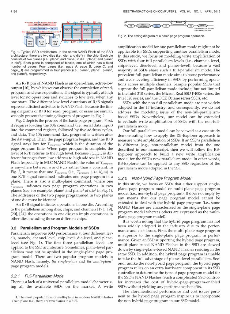
Fig. 1 shows the architecture of a typical SSD. R/B signals,one of which is contained in one die, indicate the status ofdies in NAND Flash. A low-level R/B signal indicates thatan operation command in the die is in progress.
SUN ET AL.: RB-EXPLORER: AN ACCURATE AND PRACTICAL APPROACH TOWRITE AMPLIFICATION MEASUREMENT FOR SSDS 1135
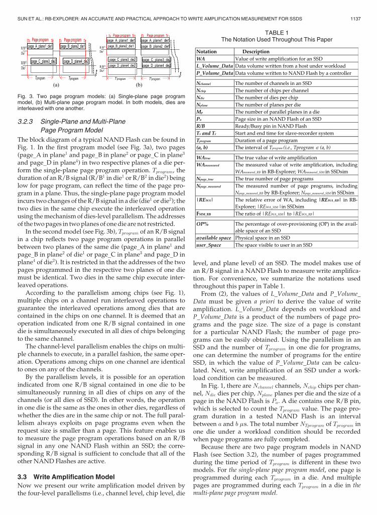
An R/B pin of NAND Flash is an open-drain, active-lowoutput [10], by whichwe can observe the completion of read,program, and erase operations. The signal is typically at highlevel for no operations and switches to low level when anyone starts. The different low-level durations of R/B signalsrepresent distinct activities in NAND Flash. Because the tim-ing diagrams of R/B for read, program, or erase are similar,we only present the timing diagram of program in Fig. 2.
Fig. 2 depicts the process of the basic page program. First,it requires loading the 80h command (i.e., serial data input)into the command register, followed by five address cycles,and data. The 10h command (i.e., program) is written afterthe data-input. Then, the page program begins, and the R/Bsignal stays low for Tprogram, which is the duration of thepage program time. When page program is complete, thelevel of R/B returns to the high level. Because Tprogram is dif-ferent for pages from low address to high address in NANDFlash (especially in MLC NAND Flash), the value of Tprogram
is anywhere between a and b ms rather than a constant. InFig. 2, it means that one Tprogram (i.e., Tprogram 2 ða; bÞmsÞ inone R/B signal contained indicates one page program in aplane. There is also a multi-plane command, where oneTprogram indicates two page program operations in twoplanes (see, for example, plane1 and plane2 of die1 in Fig. 1).The addresses of the two pages programmed in two planesof one die must be identical.
An R/B signal indicates operations in one die. Accordingto the parallelism among dies, chips, and channels [17], [19],[20], [24], the operations in one die can imply operations inother dies including those on different chips.
3.2 Parallelism and Program Models of SSDs
Parallelism improves SSD performance at four different lev-els, namely, channel-level, chip-level, die-level, and plane-level (see Fig. 1). The first three parallelism levels areapplied to the SSD architecture. Sometimes, plane-level par-allelism may not be applied in the single-plane page pro-gram model. There are two popular program models inNAND Flash, namely, the single-plane and the multi-plane1
page program models.
3.2.1 Full-Parallelism Mode
There is a lack of a universal parallelismmodel characteriz-ing all the available SSDs on the market. A write
amplification model for one parallelism mode might not beapplicable for SSDs supporting another parallelism mode.In this study, we focus on modeling write amplification ofSSDs with four full-parallelism levels (i.e., channels-level,chips-level, dies-level, and planes-level), because a vastmajority of SSDs share such a full-parallelism mode. Theprevalent full-parallelism mode aims to boost performanceand wear-leveling efficiency in SSDs by performing opera-tions across multiple channels. Sample popular SSDs thatsupport the full-parallelism mode include, but not limitedto the Intel 310 series, the Micron Real SSD P400e series, theIntel 520 series, and the OCZ Octane series SSDs, etc.
SSDs with the non-full-parallelism mode are not widelyadopted in the IT industry; and consequently, we do notaddress the modeling issue of the non-full-parallelism-based SSDs. Nevertheless, our model can be extendedto evaluate write amplification of SSDs with the non-full-parallelism mode.
Our full-parallelism model can be viewed as a case studydemonstrating how to apply the RB-Explorer approach tomeasure write amplification of SSDs. If an SSD’s parallelismis different (e.g., non-parallelism mode) from the onedescribed in our manuscript, then we will follow the RB-Explorer approach to build a new write amplificationmodel for the SSD’s new parallelism mode. In other words,RB-Explorer can be applied to any SSD regardless of theparallelism mode adopted in the SSD.
3.2.2 Non-Hybrid Page Program Model
In this study, we focus on SSDs that either support single-plane page program model or multi-plane page programmodel (i.e., non-hybrid page program). It does not imply byany means that our page program model cannot beextended to deal with the hybrid page program (i.e., someNAND Flashes are characterized as the single-plane pageprogram model whereas others are expressed as the multi-plane page program model).
It is worth noting that the hybrid page program has notbeen widely adopted in the industry due to the perfor-mance and cost issues. First, the multi-plane page programis superior to the single-plane page program in perfor-mance. Given an SSD supporting the hybrid page program,multi-plane-based NAND Flashes in the SSD are sloweddown by single-plane-based NAND Flashes residing in thesame SSD. In addition, the hybrid page program is unableto take the full advantage of planes-level parallelism. Sec-ond, unlike the non-hybrid page program, the hybrid pageprogram relies on an extra hardware component in its SSDcontroller to determine the type of page program model forthe SSD’s NAND Flashes. Such a complicated SSD control-ler increases the cost of hybrid-page-program-enabledSSDs without yielding any performance benefits.
The aforementioned performance and cost issues perti-nent to the hybrid page program inspire us to incorporatethe non-hybrid page program in our SSD model.
Fig. 2. The timing diagram of a basic page program operation.
Fig. 1. Typical SSD architecture. In the above NAND Flash of the SSDarchitecture, there are two dies (i.e., die1 and die2) in the chip. Each dieconsists of two planes (i.e., plane1 and plane2 in die1; plane3 and plane4
in die2). Each plane is composed of blocks, one of which has a fixednumber of pages. Four pages (i.e., page_A, page_B, page_C, andpage_D) are programmed in four planes (i.e., plane1, plane2, plane3,and plane4), respectively.
1. The most popular form of multi-plane in modern NAND Flashesis two-plane (i.e., there are two planes in a die).
1136 IEEE TRANSACTIONS ON COMPUTERS, VOL. 64, NO. 4, APRIL 2015
3.2.3 Single-Plane and Multi-Plane
Page Program Model
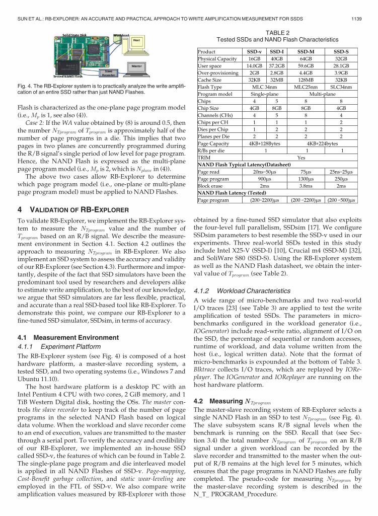
The block diagram of a typical NAND Flash can be found inFig. 1. In the first program model (see Fig. 3a), two pages(page_A in plane1 and page_B in plane2 or page_C in plane3
and page_D in plane4) in two respective planes of a die per-form the single-plane page program operation. Tprogram, theduration of an R/B signal (R/B1 in die1 or R/B2 in die2) beinglow for page program, can reflect the time of the page pro-gram in a plane. Thus, the single-plane page programmodelincurs two changes of theR/B signal in a die (die1 or die2); thetwo dies in the same chip execute the interleaved operationusing themechanismof dies-level parallelism. The addressesof the twopages in twoplanes of onedie are not restricted.
In the secondmodel (see Fig. 3b), Tprogram of an R/B signalin a chip reflects two page program operations in parallelbetween two planes of the same die (page_A in plane1 andpage_B in plane2 of die1 or page_C in plane3 and page_D inplane4 of die2). It is restricted in that the addresses of the twopages programmed in the respective two planes of one diemust be identical. Two dies in the same chip execute inter-leaved operations.
According to the parallelism among chips (see Fig. 1),multiple chips on a channel run interleaved operations toguarantee the interleaved operations among dies that arecontained in the chips on one channel. It is deemed that anoperation indicated from one R/B signal contained in onedie is simultaneously executed in all dies of chips belongingto the same channel.
The channel-level parallelism enables the chips on multi-ple channels to execute, in a parallel fashion, the same oper-ation. Operations among chips on one channel are identicalto ones on any of the channels.
By the parallelism levels, it is possible for an operationindicated from one R/B signal contained in one die to besimultaneously running in all dies of chips on any of thechannels (or all dies of SSD). In other words, the operationin one die is the same as the ones in other dies, regardless ofwhether the dies are in the same chip or not. The full paral-lelism always exploits on page programs even when therequest size is smaller than a page. This feature enables usto measure the page program operations based on an R/Bsignal in any one NAND Flash within an SSD; the corre-sponding R/B signal is sufficient to conclude that all of theother NAND Flashes are active.
3.3 Write Amplification Model
Now we present our write amplification model driven bythe four-level parallelisms (i.e., channel level, chip level, die
level, and plane level) of an SSD. The model makes use ofan R/B signal in a NAND Flash to measure write amplifica-tion. For convenience, we summarize the notations usedthroughout this paper in Table 1.
From (2), the values of L_Volume_Data and P_Volume_Data must be given a priori to derive the value of writeamplification. L_Volume_Data depends on workload andP_Volume_Data is a product of the numbers of page pro-grams and the page size. The size of a page is constantfor a particular NAND Flash; the number of page pro-grams can be easily obtained. Using the parallelism in anSSD and the number of Tprogram in one die for programs,one can determine the number of programs for the entireSSD, in which the value of P_Volume_Data can be calcu-lated. Next, write amplification of an SSD under a work-load condition can be measured.
In Fig. 1, there are Nchannel channels, Nchip chips per chan-nel, Ndie dies per chip, Nplane planes per die and the size of apage in the NAND Flash is Pa. A die contains one R/B pin,which is selected to count the Tprogram value. The page pro-gram duration in a tested NAND Flash is an intervalbetween a and b ms. The total number NTprogram of Tprogram inone die under a workload condition should be recordedwhen page programs are fully completed.
Because there are two page program models in NANDFlash (see Section 3.2), the number of pages programmedduring the time period of Tprogram is different in these twomodels. For the single-plane page program model, one page isprogrammed during each Tprogram in a die. And multiplepages are programmed during each Tprogram in a die in themulti-plane page program model.
(a) (b)
Fig. 3. Two page program models: (a) Single-plane page programmodel, (b) Multi-plane page program model. In both models, dies areinterleaved with one another.
TABLE 1The Notation Used Throughout This Paper
SUN ET AL.: RB-EXPLORER: AN ACCURATE AND PRACTICAL APPROACH TOWRITE AMPLIFICATION MEASUREMENT FOR SSDS 1137

According to the die-level parallelism, the numbers ofpage programs in two dies of one chip are approximatelyequal, meaning that Tprogram in each R/B of two dies is thesame during the page program. The number of page pro-grams is equal to each other between two dies of the samechip. The same relationship holds true for any two dies ofthe same NAND Flash in an SSD (see Fig. 1) based on thechips-level and channels-level parallelism. The concurrencyof Nchannel channels in the SSD ensures this relationshipbetween any two dies whether they are contained in thesame NAND Flash or not. The number of Tprogram based onan R/B signal can be used to measure the number of pageprograms in one die under a workload. The same relation-ship in dies of all NAND Flashes in the SSD allows us to cal-culate the total number of page programs on the SSD underthe workload.
Given a workload condition, the write amplificationmodel derives the total number of page programs using theR/B signal of a die in one NAND Flash. Thus, the modelcounts the number NTprogram of Tprogram and obtains thenumber Mp of parallel planes in a die. The total number Np
of page programs during each Tprogram, can be computed as
Np ¼ NTprogram �Mp; (3)
where the value of Mp depends on the page program model(see Section 3.2.3) in the tested NAND Flash. As shown in(4), Mp is 1 for the single-plane page program model; Mp
equals to Nplane when it comes to the multi-plane page pro-gram model. An approach to quantifying Mp is detailed inSection 3.5
Mp ¼ 1 single-plane page programmodel;Nplane multi-plane concurrent page programmodel:
�
(4)
Let Pa denote the size of one page; we can calculate thedata volume written by an SSD controller to one die as (i.e.,ðNp � PaÞ). For the NAND Flashes in the SSD, there is oneR/B pin per die. Given a chip consisting of Ndie dies, thenumber of R/B pins in the chip isNdie.
The number of R/B pins in a channel is a product of Ndie
and the number Nchip of NAND Flashes in the channel. Inother words, the number of R/B pins in the channel isðNchip �NdieÞ. Given the parallelism of dies, chips, andchannels, multiple (i.e., ðNchannel �Nchip �NdieÞ) dies areidentical. Hence, the data volume, P_Volume_Data, writtento all the NAND Flashes of the SSD is a product ofNchannel; Nchip; Ndie; Np, and Pa. Thus, we have
P Volume Data ¼ Nchannel �Nchip �Ndie �Np � Pa: (5)
It follows from (3) that
P Volume Data ¼ Nchannel �Nchip �Ndie
� NTprogram �Mp
� �� Pa: (6)
Using L_Volume_Data, Pa, NTprogram, and Tprogram, wequantify the write amplification (see also (2)) of an SSD as
WA ¼ P Volume Data
L Volume Data
¼ Nchannel �Nchip �Ndie � Pa � ðNTprogram �MpÞL Volume Data
:
(7)
Recall that L_Volume_Data in (7) is the data volume writ-ten from a host to the SSD under specific workload. L_Volu-me_Data can be measured in the form of read and write loadon the SSD. Nchip is a constant for an SSD; Ndie and Pa areconstants for a NAND Flash. NTprogram can be assessed asthe number of Tprogram on an R/B signal.Mp—the number ofparallel planes in a die—can be obtained as the number ofpage programs in one die of one tested NAND Flash duringa time period of Tprogram in the SSD. Please refer to Section3.1 for a way of measuring the number of page programs bythe Tprogram of an R/B signal.
3.4 Quantifying NNTTprogram
To obtain the value of NTprogram in the model described inSection 3.3, we need to test a single R/B in one NAND Flashof an SSD (see the justifications in Section 3.2.3). The R/Bsignal levels are scanned when workload is loaded on theSSD. Without operations, the output level of R/B is high.When an operation begins, the level of R/B becomes low,the RB-Explorer system records the starting time Ts. Whenthe R/B level changes to high, time Te value is recorded (seeFig. 3). The low level’s duration (i.e., Tprogram) is calculatedby the system as Tprogram ¼ Ts � Te. If Tprogram 2 ða; bÞms, onepage is programmed. In doing so, the total numberNTprogram of Tprogram on an R/B signal under a workload con-dition can be counted. Thus, the value of NTprogram isobtained by our RB-Explorer.
3.5 Quantifying MMp
From (4), the value of Mp depends on the page programmodels (e.g., single-plane or multi-plane page programmodel). Our RB-Explorer follows a two-step process to deter-mine the value ofMp from themeasuredwrite amplification.
Step 1: RB-Explorer executes a micro-benchmark with anincompressible sequential access and fixed amount (e.g.,2 GB) of written data on an SSD. RB-Explorer keeps track ofthe number NTprogram of low levels for page programs in anR/B signal of one NAND Flash in the SSD. Applying ourwrite amplification model (see (7) in Section 3.3), RB-Explorer obtains the value of write amplification (i.e., WA)for the SSD under this micro-benchmark using (8):
WA ¼ Nchannel �Nchip �Ndie � Pa�L Volume Data
�NTprogram : (8)
Step 2: the value ofMp can be decided by the write ampli-fication measured in Step 1. In particular, if the write ampli-fication value is approximately 1, Mp is 1; otherwise, Mp isset to 2.
Now we explain the rationale behind Step 2. Given anSSD, our micro-benchmark featured with incompressiblesequential accesses makes the write amplification close toone. In practice, whether the write amplification providedby (8) equals to one largely depends on NTprogram. Let usconsider the following two cases:
Case 1: If the WA value computed by (8) is approximately1, then the number NTprogram of Tprogram is equal to the num-ber of page programs in a die. In this case, we conclude thatonly one page in a plane is programmed during one periodof the R/B low level for page program. Thus, the NAND
1138 IEEE TRANSACTIONS ON COMPUTERS, VOL. 64, NO. 4, APRIL 2015
Flash is characterized as the one-plane page program model(i.e.,Mp is 1, see also (4)).
Case 2: If theWA value obtained by (8) is around 0.5, thenthe number NTprogram of Tprogram is approximately half of thenumber of page programs in a die. This implies that twopages in two planes are concurrently programmed duringthe R/B signal’s single period of low level for page program.Hence, the NAND Flash is expressed as the multi-planepage programmodel (i.e.,Mp is 2, which isNplane in (4)).
The above two cases allow RB-Explorer to determinewhich page program model (i.e., one-plane or multi-planepage program model) must be applied to NAND Flashes.
4 VALIDATION OF RB-EXPLORER
To validate RB-Explorer, we implement the RB-Explorer sys-tem to measure the NTprogram value and the number ofTprogram based on an R/B signal. We describe the measure-ment environment in Section 4.1. Section 4.2 outlines theapproach to measuring NTprogram in RB-Explorer. We alsoimplement an SSD system to assess the accuracy and validityof our RB-Explorer (see Section 4.3). Furthermore and impor-tantly, despite of the fact that SSD simulators have been thepredominant tool used by researchers and developers aliketo estimate write amplification, to the best of our knowledge,we argue that SSD simulators are far less flexible, practical,and accurate than a real SSD-based tool like RB-Explorer. Todemonstrate this point, we compare our RB-Explorer to afine-tuned SSD simulator, SSDsim, in terms of accuracy.
4.1 Measurement Environment
4.1.1 Experiment Platform
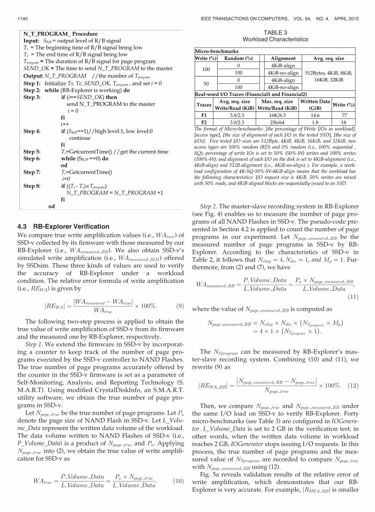
The RB-Explorer system (see Fig. 4) is composed of a hosthardware platform, a master-slave recording system, atested SSD, and two operating systems (i.e., Windows 7 andUbuntu 11.10).
The host hardware platform is a desktop PC with anIntel Pentium 4 CPU with two cores, 2 GiB memory, and 1TiB Western Digital disk, hosting the OSs. The master con-trols the slave recorder to keep track of the number of pageprograms in the selected NAND Flash based on logicaldata volume. When the workload and slave recorder cometo an end of execution, values are transmitted to the masterthrough a serial port. To verify the accuracy and credibilityof our RB-Explorer, we implemented an in-house SSDcalled SSD-v, the features of which can be found in Table 2.The single-plane page program and die interleaved modelis applied in all NAND Flashes of SSD-v. Page-mapping,Cost-Benefit garbage collection, and static wear-leveling areemployed in the FTL of SSD-v. We also compare writeamplification values measured by RB-Explorer with those
obtained by a fine-tuned SSD simulator that also exploitsthe four-level full parallelism, SSDsim [17]. We configureSSDsim parameters to best resemble the SSD-v used in ourexperiments. Three real-world SSDs tested in this studyinclude Intel X25-V (SSD-I) [10], Crucial m4 (SSD-M) [32],and SoliWare S80 (SSD-S). Using the RB-Explorer systemas well as the NAND Flash datasheet, we obtain the inter-val value of Tprogram (see Table 2).
4.1.2 Workload Characteristics
A wide range of micro-benchmarks and two real-worldI/O traces [23] (see Table 3) are applied to test the writeamplification of tested SSDs. The parameters in micro-benchmarks configured in the workload generator (i.e.,IOGenerator) include read-write ratio, alignment of I/O onthe SSD, the percentage of sequential or random accesses,runtime of workload, and data volume written from thehost (i.e., logical written data). Note that the format ofmicro-benchmarks is expounded at the bottom of Table 3.Blktrace collects I/O traces, which are replayed by IORe-player. The IOGenerator and IOReplayer are running on thehost hardware platform.
4.2 Measuring NNTprogram
The master-slave recording system of RB-Explorer selects asingle NAND Flash in an SSD to test NTprogram (see Fig. 4).The slave subsystem scans R/B signal levels when thebenchmark is running on the SSD. Recall that (see Sec-tion 3.4) the total number NTprogram of Tprogram on an R/Bsignal under a given workload can be recorded by theslave recorder and transmitted to the master when the out-put of R/B remains at the high level for 5 minutes, whichensures that the page programs in NAND Flashes are fullycompleted. The pseudo-code for measuring NTprogram bythe master-slave recording system is described in theN_T_ PROGRAM_Procedure.
Fig. 4. The RB-Explorer system is to practically analyze the write amplifi-cation of an entire SSD rather than just NAND Flashes.
TABLE 2Tested SSDs and NAND Flash Characteristics
SUN ET AL.: RB-EXPLORER: AN ACCURATE AND PRACTICAL APPROACH TOWRITE AMPLIFICATION MEASUREMENT FOR SSDS 1139
4.3 RB-Explorer Verification
We compare true write amplification values (i.e., WAture) ofSSD-v collected by its firmware with those measured by ourRB-Explorer (i.e., WAmeasured RB). We also obtain SSD-v’ssimulated write amplification (i.e., WAmeasured SIM ) offeredby SSDsim. These three kinds of values are used to verifythe accuracy of RB-Explorer under a workloadcondition. The relative error formula of write amplification(i.e., REWA) is given by
REWAj j ¼ WAmeasured �WAtruej jWAtrue
� 100%: (9)
The following two-step process is applied to obtain thetrue value of write amplification of SSD-v from its firmwareand the measured one by RB-Explorer, respectively.
Step 1. We extend the firmware in SSD-v by incorporat-ing a counter to keep track of the number of page pro-grams executed by the SSD-v controller to NAND Flashes.The true number of page programs accurately offered bythe counter in the SSD-v firmware is set as a parameter ofSelf-Monitoring, Analysis, and Reporting Technology (S.M.A.R.T). Using modified CrystalDiskInfo, an S.M.A.R.T.utility software, we obtain the true number of page pro-grams in SSD-v.
LetNpage true be the true number of page programs. Let Pa
denote the page size of NAND Flash in SSD-v. Let L_Volu-me_Data represent the written data volume of the workload.The data volume written to NAND Flashes of SSD-v (i.e.,P_Volume_Data) is a product of Npage true and Pa. ApplyingNpage true into (2), we obtain the true value of write amplifi-cation for SSD-v as
WAtrue ¼ P Volume Data
L Volume Data¼ Pa �Npage true
L Volume Data: (10)
Step 2. The master-slave recording system in RB-Explorer(see Fig. 4) enables us to measure the number of page pro-grams of all NAND Flashes in SSD-v. The pseudo-code pre-sented in Section 4.2 is applied to count the number of pageprograms in our experiment. Let Npage measured RB be themeasured number of page programs in SSD-v by RB-Explorer. According to the characteristics of SSD-v inTable 2, it follows that Nchip ¼ 4; Ndie ¼ 1, and Mp ¼ 1. Fur-thermore, from (2) and (7), we have
WAmeasured RB ¼ P Volume Data
L Volume Data¼ Pa �Npage measured RB
L Volume Data;
(11)
where the value ofNpage measured RB is computed as
Npage measured RB ¼ Nchip �Ndie � NTprogram �Mp
� �¼ 4� 1� NTprogram � 1
� �:
The NTprogram can be measured by RB-Explorer’s mas-ter-slave recording system. Combining (10) and (11), werewrite (9) as
REWA RBj j ¼ Npage measured RB �Npage true
�� ��Npage true
� 100%: (12)
Then, we compare Npage true and Npage measured RB underthe same I/O load on SSD-v to verify RB-Explorer. Fortymicro-benchmarks (see Table 3) are configured in IOGenera-tor. L_Volume_Data is set to 2 GB in the verification test; inother words, when the written data volume in workloadreaches 2 GB, IOGenerator stops issuing I/O requests. In thisprocess, the true number of page programs and the mea-sured value of NTprogram are recorded to compare Npage true
with Npage measured RB using (12).Fig. 5a reveals validation results of the relative error of
write amplification, which demonstrates that our RB-Explorer is very accurate. For example, jREWA RBj is smaller
TABLE 3Workload Characteristics
1140 IEEE TRANSACTIONS ON COMPUTERS, VOL. 64, NO. 4, APRIL 2015

than 1 percent (i.e., jREWA RBj < 1%) in write-intensivemicro-benchmarks, and jREWA RBj is smaller than 10 per-cent (i.e., jREWA RBj < 10%) in the read/write mixedmicro-benchmarks. The validation results confirm the accu-racy and credibility of our RB-Explorer. Thus, RB-Explorercan be employed to measure write amplification for SSDsunder any I/O workload. The small value of jREWA RBj isattributed to the following three reasons.
First, the typical latency erase is around 2 ms for NANDFlash in SSD-v. Interestingly, the latency for a program isanywhere between 200 and 2,200 ms, which makes pro-gram and erase time interleaved. Hence, the times of erasesmay be added to the number of programs. Thus, the errorof an excessive number of programs may exit. Let usassume that the duration of page program distributes I.I.D.according to a uniform distribution as Unif [200, 2,200].The probability of the duration of block erase being in therange from 200 to 2,200 is 10 percent; this probability ismuch smaller in real cases. In Fig. 5a, our empirical resultsconfirm that the influence of interleaved duration of pro-gram and erase is insignificant.
Second, the sampling process for R/B signals may misssome low levels for page program, making the number ofpage programs smaller.
Third, there is a distinction between the programdurationsof lower-addressed pages and those of upper-addressedpages inside NAND Flash. Lower-addressed pages haveshorter programdurations than upper-addressed pages’ pro-gram durations.
The plane-level parallelism, the lowest level of paral-lelism level, is independent of the other three levels ofparallelism. The multi-plane model is physically distinctfrom the one-plane model. Nevertheless, the verificationof the one-plane model can be used to verify the multi-plane model.
4.4 Improving on Accuracy of SSDsim
Now we demonstrate that RB-Explorer is more accuratethan a state-of-the-art SSD simulator—SSDsim. We tuneSSDsim’s parameter to simulate SSD-v and collect SSD-v’ssimulated write amplification (i.e., WAmeasured SIM ). We runIOGenerator to drive both SSDsim and SSD-v; we assess thenumber of page programs (i.e., Npage measured SIM ) from anoutput file for the comparison purpose. Comparing REWA
of WAmeasured SIM and REWA of WAmeasured RB, we concludethat RB-Explorer is more accurate than SSDsim in terms ofmeasuring SSD write amplification.
Similar to (11) and (12), the relative error formula of writeamplification for SSDsim is written as
REWA SIMj j ¼ Npage measured SIM �Npage true
�� ��Npage true
� 100%: (13)
Fig. 5b plots the experimental results from the simulator.Except for the 4 KiB-100 percent-W-align_RD case, all thecases under the 100 percent-write workload have smalljREWA SIM j (i.e., jREWA SIM j < 5%). Unfortunately, mostjREWA SIM j values in other cases are larger than 14 percentunder the 50 percent-write workload. These values inFig. 5b are much larger than those in Fig. 5a. In order toquantify the difference between jREWA RBj and jREWA SIM j,we introduce
FSIM RB ¼ REWA SIMj jREWA RBj j ; (14)
where FSIM RB is the deviation ratio of the write amplifica-tion value measured by the simulator to that measured byRB-Explorer. Obviously, the larger the FSIM RB values are,the more accurate RB-Explorer is than SSDsim. Fig. 5creveals that in a few cases, SSDsim’s accuracy is slightlyhigher than that of RB-Explorer, because SSDsim does notconsider the interleaved time between program and eraseoperations, however small it may be. Fig. 5c also confirmsthat the accuracy of our RB-Explorer is much higher thanthat of SSDsim in most tested cases.
RB-Explorer improves on the accuracy of SSDsimbecause of the following three reasons: First, the event-driven-based SSDsim does not accurately resemble real-world SSDs from the perspective of bursty random-write I/Os; thus, SSDsim inaccurately simulates the frequency ofgarbage collection. Second, due to the initial mechanism forread operations in SSDsim, it issues a pre-write operationfor each read request. Consequently, write data volumesimulated by SSDsim is larger than that of the real-worldSSD. Third, SSDsim is unable to simulate read disturb,which triggers excessive block erases and programs.
More importantly, since any one simulator cannot uni-versally accurately simulate all SSDs, the fact that writeamplification values measured by the fine-tuned SSDsimpresent a much larger deviation from true ones implies thatsimulators in general cannot flexibly and accurately mea-sure the write amplification value.
5 EXPERIMENTAL RESULTS
Now we employ RB-Explorer to evaluate write amplifica-tion and its performance impact of three real-world SSDs(i.e., SSD-I, SSD-M, and SSD-S) during the initial andsteady states, respectively. Write amplification values
(a) (b) (c)
Fig. 5. Relative error of write amplification: (a) jREWA RBj; (b) jREWA SIM j; (c) FSIM RB (i.e., ðjREWA SIM jÞ=ðjREWA RBjÞ).
SUN ET AL.: RB-EXPLORER: AN ACCURATE AND PRACTICAL APPROACH TOWRITE AMPLIFICATION MEASUREMENT FOR SSDS 1141

measured in the initial state are reference points, andthose obtained in the steady state represent standard onesfor the tested SSDs.
We use Windows 7, on which IOGenerator is running,to partition the tested SSDs with 4 KiB alignment and tosend a TRIM [15], [35] command to emulate SSD factorystate (i.e., the initial state). Blktrace and IORplayer, runningon Ubuntu 11.10, replay I/O traces. The slave recorder inRB-Explorer monitors an available R/B pin of one chip intested SSDs to test its output level for page program. IOGen-erator or IOReplayer stops issuing requests when the follow-ing two criteria are satisfied. First, the tested bandwidthmeasured in IOPS or MB/s reaches a stable value (see Sec-tion 5.1). Second, data volume written from the host satisfiesa specified requirement (see Section 5.2 and Section 5.3).The slave recorder transmits NTprogram to the master whenthe output of R/B remains at the high level for five minutes.The values of Mp are based on the program model ofNAND Flash in tested SSDs in Table 2. From (7), we canobtain the write amplification values for the SSDs under thegiven workload conditions.
5.1 Micro-Benchmarks Measurement
Micro-benchmarks in Table 3 are all selected. We select twoextreme workload conditions—full sequential and full ran-dom write cases, labeled “SQ” and “RD” respectively inthe legends of the write amplification curves of Figs. 6, 7, 8,and 9. The I/O access patterns of other micro-benchmarksare between these two extreme cases. To evaluate theimpact of read I/Os on write amplification, we choose50 percent-read micro-benchmarks. Tested SSDs areopened with O_DIRECT.
5.1.1 SSD Measurement in the Initial State
In the initial state, write amplification obtained by RB-Explorer is very small, because there is sufficient amount ofavailable space for write I/Os to incur only infrequent gar-bage collection when data is updated. In additional, the val-ues plotted in Figs. 6 and 7 are very low under sequential
accesses. This result is attributed to the fact that SSDs takeadvantage of sequential accesses, which may incur less fre-quent but highly efficient garbage collection during pageprograms. Thus, these workload conditions help SSDsmaintain low write amplification.
When the I/O size is small (see the 512-Byte results inFigs. 6 and 7), we found write amplification to be muchhigher than that under the sequential or random workloadwith big I/Os (e.g., I/O size from 4 to 32 KiB). Data vol-umes written per I/O transaction smaller than the pagesize (i.e., 4 KiB) trigger more page programs in NANDFlash, which increases write amplification. Our 512-Byteresults also show that write amplification values under 4KiB-align_SQ accesses are larger than those under 4 KiB-no-align_SQ accesses. The 4 KiB-align alignment is a bur-den in the case of sequential accesses of small I/Os.Because the alignment size of each I/O on the SSD is 4KiB, they will begin at a multiple of 4 KiB from the begin-ning of an SSD. The size of the page is 4 KiB, but this typeof I/Os cannot be programmed in the same page. In thiscase, the number of page programs increases and writeamplification is larger under 4 KiB-align_SQ accesses thanthat under 4 KiB-no-align_SQ accesses.
In Figs. 6a and 6b, write amplification under 512-BytesI/O random accesses is smaller than that in Fig 6c. Thecache space in SSD-I and SSD-M is 32 and 128 MB, respec-tively; and the cache is deployed to merge many small I/Osinto larger ones to reduce the number of page updates anddecrease write amplification accordingly. The cache spacefor SSD-S, 32 KB, is much smaller than that for SSD-I andSSD-M, resulting in much higher write amplification under512-Byte random I/O accesses. However, the average val-ues in the 8, 16, and 32 KiB benchmarks are much larger forSSD-M than SSD-I as shown in Figs. 6a and 6b; this mayresult from the different FTL technology.
When it comes to I/Os that are bigger than 512 Bytes (i.e.,I/O size from 4 to 32 KiB), alignment hardly impacts thewrite amplification under sequential access patterns. Theaverage value of write amplification ranges from 1.07 to1.60 under the 4 KiB-no-align_SQ accesses in Figs. 6 and 7. It
Fig. 6. Fifty percent-write micro-benchmarks in the initial state of RAW SSDs.
Fig. 7. Hundred percent-write micro-benchmarks in the initial state of RAW SSDs.
1142 IEEE TRANSACTIONS ON COMPUTERS, VOL. 64, NO. 4, APRIL 2015

can be seen that garbage collection rarely occurs, giving riseto low write amplification.
Read I/Os noticeably affect write amplification when thecache space is small (see Figs. 6c versus 7c). For SSD-I andSSD-M, the impact of read I/Os on write amplification isless noticeable. Nevertheless, the write amplification valuesplotted in Fig. 6 are larger than those in Fig. 7. The reasonfor this trend is two-fold. First, a significant portion ofDRAM is allocated to caching read data, limiting cacheresources that may boost random write performance bymerging small writes. Second, read operations in NANDFlash may cause the read disturb in blocks, meaning thatthe valid pages are rewritten before erasing the blocks. Thisenlarges write amplification.
5.1.2 SSD Measurement in the Steady State
To place the tested SSDs in the random-steady (steady forshort) state, the 4 KiB-align_RD access is configured to dis-tribute data across the available space of NAND Flashes asunevenly as possibly for about 12 hours.
In the steady state, Figs. 8 and 9 demonstrate that writeamplification is very low in the case of sequential accesses.The average value of write amplification is anywherebetween 1 and 5 except for the workload with 512-Bytesrequests. In the process of random accesses, write amplifica-tion is between 10 and 50. The worst-case write amplificationvalues all happen with 512-Byte I/O requests. In addition tosmall I/O sizes and random accesses, lack of sufficient dataspace for written data can aggravate write amplification. Inthis test, the capacity of over-provisioning (i.e., OP, the inclu-sion of extra storage capacity in NAND Flashes that isreserved only for SSD controllers) is an important factoraffecting the write amplification for SSDs with less dataspace. OP lowers write amplification and makes the changesof values smooth (see the results from SSD-M).
Write amplification of SSD-M with a 128 MB cache variesslightly more than that of SSD-I with a 32 MB cache. SSD-Swith a 32 KB cache becomes the worst case. The maximumwrite amplification changes from 85 to 90 for SSD-M (seeFigs. 8b and 9b) but ranges from 110 to 150 for SSD-S (see
Figs. 8c and 9c). This indicates that write amplification issensitive to cache size.
Comparing with the 100 percent-write workload, theread I/Os in the 50 percent-write workload elevate writeamplification in the steady state. Although write amplifica-tion decreases when I/O size increases, it is still higher thanthat under the 100 percent-write workload. Please refer toSection 5.1.1 for the reasons why read I/Os increase writeamplification.
Since the tests for different SSDs are similar, our remain-ing tests are focused only on one SSD-I withMp ¼ 1.
5.2 Logical Data Volume in Partitioned SSDs
The logical data volume written from the host substantiallyaffects write amplification. A large amount of data writtento NAND Flash space leads to limited user-data space,which increases the probability of page updates and the fre-quency of garbage collection. This trend becomes pro-nounced under random workload conditions, whichincreases write amplification. Thus, the relationship betweenwrite amplification of an SSD and logical data volume writtenfrom the host (WALVD) is important in deepening this under-standing and thus investigated in this paper.
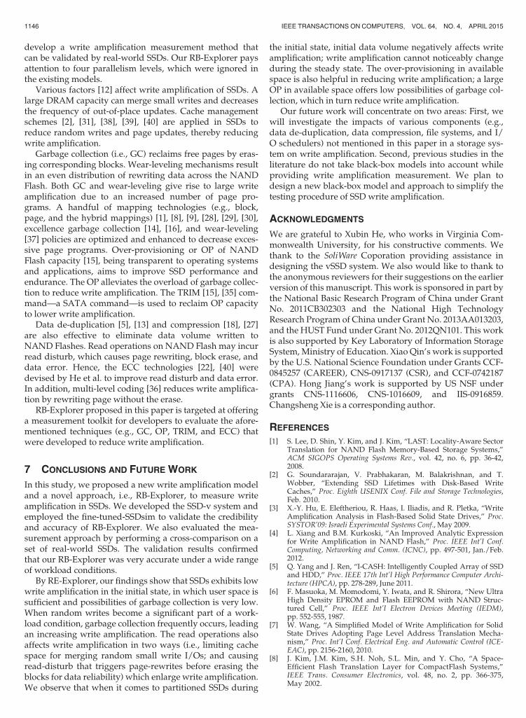
In this test procedure, we focus on WALVD under fivekinds of OP percent. Although the OP costs extra capacityin NAND Flashes, it is employed to reduce write amplifica-tion of SSDs. Under a given OP percent condition, we runthe 4 KiB-align_RD access test for 15 times, in each of whichthe 5 GiB logical written data volume is configured byIOGenerator. After the amount of written data satisfies therequirement, the IOGenerator stops sending requests. TheNTprogram is transmitted to the master by the slave recorderwhen the output of R/B remains at the high level for fiveminutes. After the master receives the result, the next sub-test will start. Fifteen sub-tests will be performed duringeach experiment. From (7), we derive write amplificationfrom L_Volume_Data (5 GiB) and the value ofNTprogram.
There is a 40 GB capacity in the partitioned SSD-I with37.2 GB user space. Seven percent of the total capacity (i.e.,2.8 GB) is set as the OP space. The available space, in this
Fig. 8. Fifty percent-write micro-benchmarks in the steady state of RAW SSDs.
Fig. 9. Hundred percent-write micro-benchmarks in the steady state of RAW SSDs.
SUN ET AL.: RB-EXPLORER: AN ACCURATE AND PRACTICAL APPROACH TOWRITE AMPLIFICATION MEASUREMENT FOR SSDS 1143
paper, includes user space and OP space. For SSD-I, the rela-tionship between the OP percent in the available space ofSSD and write amplification is given as
OP% ¼ OP � 100%
Available Space¼ OP � 100%
OP þ User Space
¼ 2:8GB
2:8GBþ User Space� 100%;
(15)
where OP space cannot be changed by users; however, theOP percent in the available space can be configured by mod-ifying the user space size on the right-hand side of (15).Table 4 illustrates how we configure the user-space parame-ters. In each test, we initialize the SSDs to their factorydefault states by the TRIM command and partition accord-ing to the user-space size or User_Space (see (15)).
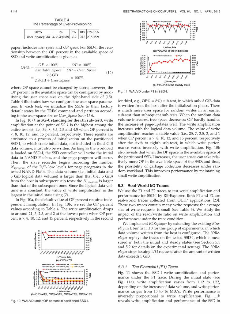
In Fig. 10 (k in 5G-k standing for the kth sub-test), writeamplification at the point of 5G-1 is the highest among theentire test set, i.e., 39, 8, 6.5, 2.5 and 4.5 when OP percent is7, 8, 10, 12, and 15 percent, respectively. These results areattributed to a process of initialization on the partitionedSSD-I, to which some initial data, not included in the 5 GiBdata volume, must also be written. As long as the workloadis loaded on SSD-I, the SSD controller will write the initialdata to NAND Flashes, and the page program will occur.Then, the slave recorder begins recording the numberNTprogram of the R/B low levels for page programs in thetested NAND Flash. This data volume (i.e., initial data and5 GiB logical data volume) is larger than that (i.e., 5 GiB)from the host in subsequent sub-tests; the NTprogram is largerthan that of the subsequent ones. Since the logical data vol-ume is a constant, the value of write amplification is thelargest in the initial state using (7).
In Fig. 10a, the default value of OP percent requires inde-pendent manipulation. In Fig. 10b, we set the OP percentvalues according to Table 4. The write amplification dropsto around 21, 3, 2.5, and 2 at the lowest point when OP per-cent is 7, 8, 10, 12, and 15 percent, respectively in the second
(or third, e.g., OP% ¼ 8%) sub-test, in which only 5 GiB datais written from the host after the initialization phase. Thereis much more user space for random writes in an earliersub-test than subsequent sub-tests. When the random datavolume increases, free space decreases; OP hardly handlesthe increase of page-updates well. The write amplificationincreases with the logical data volume. The value of writeamplification reaches a stable value (i.e., 25, 7, 3.5, 3, and 1when OP percent is 7, 8, 10, 12, and 15 percent, respectivelyafter the sixth to eighth sub-test), in which write perfor-mance varies inversely with write amplification. Fig. 10balso reveals that when the OP space in the available space ofthe partitioned SSD-I increases, the user space can take rela-tively more OP in the available space of the SSD; and thus,the possibility of garbage collection decreases under ran-dom workload. This improves performance by maintainingsmall write amplification.
5.3 Real-World I/O Traces
We use the F1 and F2 traces to test write amplification andperformance for SSD-I by RB-Explorer. Both F1 and F2 arereal-world traces collected from OLTP applications [23].These two traces contain many write requests; the averagesize of write requests is small (see Table 3). We study theimpact of the read/write ratio on write amplification andperformance under the trace condition.
We implement IOReplayer by extending the existing Btre-play in Ubuntu 11.10 for this group of experiments, in whichdata volume written from the host is configured. The IORe-player replays the traces on the tested SSD-I, which is mea-sured in both the initial and steady states (see Section 5.1and 5.2 for details on the experimental setting). The IORe-player stops issuing I/O requests after the amount of writtendata exceeds 5 GiB.
5.3.1 The Financial1 (F1) Trace
Fig. 11 shows the SSD-I write amplification and perfor-mance under the F1 trace. During the initial state (seeFig. 11a), write amplification varies from 1.12 to 1.22,depending on the increase of data volume, and write perfor-mance ranges from 13 to 16 MB/s. Write performance isinversely proportional to write amplification. Fig. 11breveals write amplification and performance of the SSD in
TABLE 4The Percentage of Over-Provisioning
Fig. 10. WALVD under OP percent in partitioned SSD-I.
Fig. 11. WALVD under F1 in SSD-I.
1144 IEEE TRANSACTIONS ON COMPUTERS, VOL. 64, NO. 4, APRIL 2015
the steady state, in which write amplification is around 16and write throughput is about 2 MB/s in the first subtest.The poor performance is attributed to less available spaceand a random data distribution.
In the subsequent sub-tests, the write amplification andperformance become much better thanks to the write pat-tern in the trace. After the 13th sub-test, the write amplifica-tion and throughput become approximately 2 and 12 MB/s,respectively. When 77 percent of the requests are writes, thewrite performance is 16 and 12 MB/s in the initial andsteady state, respectively. The write performance in thesteady state is worse than that in the initial. The differencebetween write amplification in the initial and steady statesis insignificant.
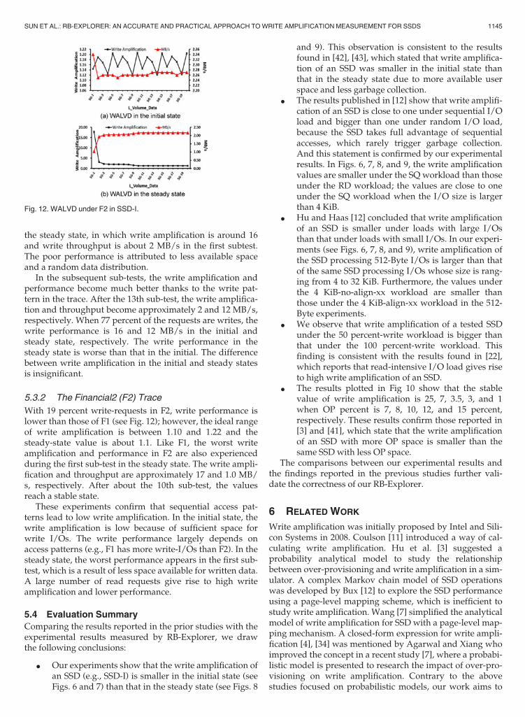
5.3.2 The Financial2 (F2) Trace
With 19 percent write-requests in F2, write performance islower than those of F1 (see Fig. 12); however, the ideal rangeof write amplification is between 1.10 and 1.22 and thesteady-state value is about 1.1. Like F1, the worst writeamplification and performance in F2 are also experiencedduring the first sub-test in the steady state. The write ampli-fication and throughput are approximately 17 and 1.0 MB/s, respectively. After about the 10th sub-test, the valuesreach a stable state.
These experiments confirm that sequential access pat-terns lead to low write amplification. In the initial state, thewrite amplification is low because of sufficient space forwrite I/Os. The write performance largely depends onaccess patterns (e.g., F1 has more write-I/Os than F2). In thesteady state, the worst performance appears in the first sub-test, which is a result of less space available for written data.A large number of read requests give rise to high writeamplification and lower performance.
5.4 Evaluation Summary
Comparing the results reported in the prior studies with theexperimental results measured by RB-Explorer, we drawthe following conclusions:
� Our experiments show that the write amplification ofan SSD (e.g., SSD-I) is smaller in the initial state (seeFigs. 6 and 7) than that in the steady state (see Figs. 8
and 9). This observation is consistent to the resultsfound in [42], [43], which stated that write amplifica-tion of an SSD was smaller in the initial state thanthat in the steady state due to more available userspace and less garbage collection.
� The results published in [12] show that write amplifi-cation of an SSD is close to one under sequential I/Oload and bigger than one under random I/O load,because the SSD takes full advantage of sequentialaccesses, which rarely trigger garbage collection.And this statement is confirmed by our experimentalresults. In Figs. 6, 7, 8, and 9, the write amplificationvalues are smaller under the SQ workload than thoseunder the RD workload; the values are close to oneunder the SQ workload when the I/O size is largerthan 4 KiB.
� Hu and Haas [12] concluded that write amplificationof an SSD is smaller under loads with large I/Osthan that under loads with small I/Os. In our experi-ments (see Figs. 6, 7, 8, and 9), write amplification ofthe SSD processing 512-Byte I/Os is larger than thatof the same SSD processing I/Os whose size is rang-ing from 4 to 32 KiB. Furthermore, the values underthe 4 KiB-no-align-xx workload are smaller thanthose under the 4 KiB-align-xx workload in the 512-Byte experiments.
� We observe that write amplification of a tested SSDunder the 50 percent-write workload is bigger thanthat under the 100 percent-write workload. Thisfinding is consistent with the results found in [22],which reports that read-intensive I/O load gives riseto high write amplification of an SSD.
� The results plotted in Fig 10 show that the stablevalue of write amplification is 25, 7, 3.5, 3, and 1when OP percent is 7, 8, 10, 12, and 15 percent,respectively. These results confirm those reported in[3] and [41], which state that the write amplificationof an SSD with more OP space is smaller than thesame SSD with less OP space.
The comparisons between our experimental results andthe findings reported in the previous studies further vali-date the correctness of our RB-Explorer.
6 RELATED WORK
Write amplification was initially proposed by Intel and Sili-con Systems in 2008. Coulson [11] introduced a way of cal-culating write amplification. Hu et al. [3] suggested aprobability analytical model to study the relationshipbetween over-provisioning and write amplification in a sim-ulator. A complex Markov chain model of SSD operationswas developed by Bux [12] to explore the SSD performanceusing a page-level mapping scheme, which is inefficient tostudy write amplification. Wang [7] simplified the analyticalmodel of write amplification for SSD with a page-level map-ping mechanism. A closed-form expression for write ampli-fication [4], [34] was mentioned by Agarwal and Xiang whoimproved the concept in a recent study [7], where a probabi-listic model is presented to research the impact of over-pro-visioning on write amplification. Contrary to the abovestudies focused on probabilistic models, our work aims to
Fig. 12. WALVD under F2 in SSD-I.
SUN ET AL.: RB-EXPLORER: AN ACCURATE AND PRACTICAL APPROACH TOWRITE AMPLIFICATION MEASUREMENT FOR SSDS 1145
develop a write amplification measurement method thatcan be validated by real-world SSDs. Our RB-Explorer paysattention to four parallelism levels, which were ignored inthe existing models.
Various factors [12] affect write amplification of SSDs. Alarge DRAM capacity can merge small writes and decreasesthe frequency of out-of-place updates. Cache managementschemes [2], [31], [38], [39], [40] are applied in SSDs toreduce random writes and page updates, thereby reducingwrite amplification.
Garbage collection (i.e., GC) reclaims free pages by eras-ing corresponding blocks. Wear-leveling mechanisms resultin an even distribution of rewriting data across the NANDFlash. Both GC and wear-leveling give rise to large writeamplification due to an increased number of page pro-grams. A handful of mapping technologies (e.g., block,page, and the hybrid mappings) [1], [8], [9], [28], [29], [30],excellence garbage collection [14], [16], and wear-leveling[37] policies are optimized and enhanced to decrease exces-sive page programs. Over-provisioning or OP of NANDFlash capacity [15], being transparent to operating systemsand applications, aims to improve SSD performance andendurance. The OP alleviates the overload of garbage collec-tion to reduce write amplification. The TRIM [15], [35] com-mand—a SATA command—is used to reclaim OP capacityto lower write amplification.
Data de-duplication [5], [13] and compression [18], [27]are also effective to eliminate data volume written toNAND Flashes. Read operations on NAND Flash may incurread disturb, which causes page rewriting, block erase, anddata error. Hence, the ECC technologies [22], [40] weredevised by He et al. to improve read disturb and data error.In addition, multi-level coding [36] reduces write amplifica-tion by rewriting page without the erase.
RB-Explorer proposed in this paper is targeted at offeringa measurement toolkit for developers to evaluate the afore-mentioned techniques (e.g., GC, OP, TRIM, and ECC) thatwere developed to reduce write amplification.
7 CONCLUSIONS AND FUTURE WORK
In this study, we proposed a new write amplification modeland a novel approach, i.e., RB-Explorer, to measure writeamplification in SSDs. We developed the SSD-v system andemployed the fine-tuned-SSDsim to validate the credibilityand accuracy of RB-Explorer. We also evaluated the mea-surement approach by performing a cross-comparison on aset of real-world SSDs. The validation results confirmedthat our RB-Explorer was very accurate under a wide rangeof workload conditions.
By RE-Explorer, our findings show that SSDs exhibits lowwrite amplification in the initial state, in which user space issufficient and possibilities of garbage collection is very low.When random writes become a significant part of a work-load condition, garbage collection frequently occurs, leadingan increasing write amplification. The read operations alsoaffects write amplification in two ways (i.e., limiting cachespace for merging random small write I/Os; and causingread-disturb that triggers page-rewrites before erasing theblocks for data reliability) which enlarge write amplification.We observe that when it comes to partitioned SSDs during
the initial state, initial data volume negatively affects writeamplification; write amplification cannot noticeably changeduring the steady state. The over-provisioning in availablespace is also helpful in reducing write amplification; a largeOP in available space offers low possibilities of garbage col-lection, which in turn reduce write amplification.
Our future work will concentrate on two areas: First, wewill investigate the impacts of various components (e.g.,data de-duplication, data compression, file systems, and I/O schedulers) not mentioned in this paper in a storage sys-tem on write amplification. Second, previous studies in theliterature do not take black-box models into account whileproviding write amplification measurement. We plan todesign a new black-box model and approach to simplify thetesting procedure of SSD write amplification.
ACKNOWLEDGMENTS
We are grateful to Xubin He, who works in Virginia Com-monwealth University, for his constructive comments. Wethank to the SoliWare Coporation providing assistance indesigning the vSSD system. We also would like to thank tothe anonymous reviewers for their suggestions on the earlierversion of this manuscript. This work is sponsored in part bythe National Basic Research Program of China under GrantNo. 2011CB302303 and the National High TechnologyResearch Program of China under Grant No. 2013AA013203,and the HUST Fund under Grant No. 2012QN101. This workis also supported by Key Laboratory of Information StorageSystem, Ministry of Education. Xiao Qin’s work is supportedby the U.S. National Science Foundation under Grants CCF-0845257 (CAREER), CNS-0917137 (CSR), and CCF-0742187(CPA). Hong Jiang’s work is supported by US NSF undergrants CNS-1116606, CNS-1016609, and IIS-0916859.Changsheng Xie is a corresponding author.
REFERENCES
[1] S. Lee, D. Shin, Y. Kim, and J. Kim, “LAST: Locality-Aware SectorTranslation for NAND Flash Memory-Based Storage Systems,”ACM SIGOPS Operating Systems Rev., vol. 42, no. 6, pp. 36-42,2008.
[2] G. Soundararajan, V. Prabhakaran, M. Balakrishnan, and T.Wobber, “Extending SSD Lifetimes with Disk-Based WriteCaches,” Proc. Eighth USENIX Conf. File and Storage Technologies,Feb. 2010.
[3] X.-Y. Hu, E. Eleftheriou, R. Haas, I. Iliadis, and R. Pletka, “WriteAmplification Analysis in Flash-Based Solid State Drives,” Proc.SYSTOR’09: Israeli Experimental Systems Conf., May 2009.
[4] L. Xiang and B.M. Kurkoski, “An Improved Analytic Expressionfor Write Amplification in NAND Flash,” Proc. IEEE Int’l Conf.Computing, Networking and Comm. (ICNC), pp. 497-501, Jan./Feb.2012.
[5] Q. Yang and J. Ren, “I-CASH: Intelligently Coupled Array of SSDand HDD,” Proc. IEEE 17th Int’l High Performance Computer Archi-tecture (HPCA), pp. 278-289, June 2011.
[6] F. Masuoka, M. Momodomi, Y. Iwata, and R. Shirora, “New UltraHigh Density EPROM and Flash EEPROM with NAND Struc-tured Cell,” Proc. IEEE Int’l Electron Devices Meeting (IEDM),pp. 552-555, 1987.
[7] W. Wang, “A Simplified Model of Write Amplification for SolidState Drives Adopting Page Level Address Translation Mecha-nism,” Proc. Int’l Conf. Electrical Eng. and Automatic Control (ICE-EAC), pp. 2156-2160, 2010.
[8] J. Kim, J.M. Kim, S.H. Noh, S.L. Min, and Y. Cho, “A Space-Efficient Flash Translation Layer for CompactFlash Systems,”IEEE Trans. Consumer Electronics, vol. 48, no. 2, pp. 366-375,May 2002.
1146 IEEE TRANSACTIONS ON COMPUTERS, VOL. 64, NO. 4, APRIL 2015

[9] A. Gupta, Y. Kim, and B. Urgaonkar, “DFTL: A Flash TranslationLayer Employing Demand-Based Selective Caching of Page-LevelAddress Mappings,” Proc. ACM Int’l Conf. Architectural Support forProgramming Languages and Operating Systems (ASPLOS), pp. 229-240, Mar. 2009.
[10] Intel MD332 NAND Flash Memory Datasheet, June 2009.[11] R. Coulson, “How Solid-State Drives Improve Computing
Platforms,”Intel IDF Fall, 2008.[12] X.-Y. Hu and R. Haas, “The Fundamental Limit of Flash Random
Write Performance: Understanding, Analysis and PerformanceModeling,” research report, RZ 3771 (# 99781), IBM Research Zur-ich, Switzerland, Mar. 2010.
[13] J. Kim, C. Lee, S. Lee, I. Son, J. Choi, S. Yoon, H.-u. Lee, S. Kang, Y.Won, and J. Cha, “De-Duplication in SSDs: Model and Quantita-tive Analysis,” Proc. IEEE 28th Symp. Mass Storage Systems andTechnologies (MSST ’12), pp. 1-12, Apr. 2012.
[14] L.-P. Chang, T.-W. Kuo, and S.-W. Lo, “Real-Time Garbage Collec-tion for Flash-Memory Storage Systems of Real-Time EmbeddedSystems,” ACM Trans. Embedded Computing Systems, vol. 3, no. 4,pp. 837-863, Nov. 2004.
[15] T. Frankie, G. Hughes, and K. Kreutz-Delgado, “SSD Trim Com-mands Considerably Improve Overprovisioning,” Proc. FlashMemory Summit’11, Aug. 2011.
[16] I. Iliadis, “Performance of the Greedy Garbage-Collection Schemein Flash-Based Solid-State Drives,” Research Report, RZ 3769 (#99779), IBM Research, Zurich, Switzerland, Mar. 2010.
[17] Y. Hu, H. Jiang, D. Feng, L. Tian, H. Luo, and S.-P. Zhang,“Performance Impact and Interplay of SSD Parallelism throughAdvanced Commands, Allocation Strategy and Data Gran-ularity,” Proc. Int’l Conf. Supercomputing (ICS ’11), pp. 96-107, May2011.
[18] T. Park and J.-S. Kim, “Compression Support for Flash TranslationLayer,” Proc. Int’l Workshop Software Support for Portable Storage,pp. 19-24, Oct. 2010.
[19] S. Park, E. Seo, J. Shin, S. Maeng, and J. Lee, “Exploiting InternalParallelism of Flash-Based SSDs,” IEEE Computer Architecture Let-ters, vol. 9, no. 1, pp. 9-12, Jan.-June 2010.
[20] F. Chen, R. Lee, and X. Zhang, “Essential Roles of Exploiting Inter-nal Parallelism of Flash Memory Based Solid State Drives in High-Speed Data Processing,” Proc. IEEE 17th Int’l High PerformanceComputer Architecture (HPCA ’11), pp. 266-277, Feb. 2011.
[21] Intel http://www.iometer.org/, 2014.[22] S. Moon and A.L.N. Reddy, “Write Amplification Due to ECC on
Flash Memory or Leave Those Bit Errors Alone,” Proc. IEEE 28thSymp. Mass Storage Systems and Technologies (MSST ’12), pp. 1-6,Apr. 2012.
[23] K. B ates and B. McNutt, “SPC: Storage Process Council I/Otraces,” UMass Trace Repository, 2008.
[24] M. Jung, E. Herbert Wilson, and M.T. Kandemir, “PhysicallyAddressed Queueing (PAQ): Improving Parallelism in Solid StateDisks,” Proc. 39th Int’l Symp. Computer Architecture (ISCA ’12),pp. 404-415, June 2012.
[25] White-box-testing, http://en.wikipedia.org/wiki/White-box_testing, 2014.
[26] A.M. Caulfield, L. M. Grupp, and S. Swanson, “Gordon: UsingFlash Memory to Build Fast, Power-Efficient Clusters for Data-Intensive Applications,” Proc. ACM Int’l Conf. Architectural Supportfor Programming Languages and Operating Systems (ASPLOS ’09),pp. 217-228, Mar. 2009.
[27] G. Wu and X. He, “Delta-FTL: Improving SSD Lifetime viaExploiting Content Locality,” Proc. Seventh ACM European Conf.Computer Systems, pp. 253-266, Apr. 2012.
[28] S.-W. Lee, D.-J. Park, T.-S Chung, D.-H. Lee, S.-W. Park, and H.-J.Song, “FAST: An FTL Scheme with Fully Associative Sector Trans-lations,” Proc. US-Korea Conf. Science, Technology & Entrepreneur-ship, Aug. 2005.
[29] J. Kang, H. Jo, J. Kim, and J. Lee, “A Superblock-Based FlashTranslation Layer for NAND Flash Memory,” Proc. Sixth ACM/IEEE Int’l Conf. Embedded Software, pp. 161-170, Oct. 2006.
[30] F. Chen, T. Luo, and X. Zhang, “CAFTL: A Content-Aware FlashTranslation Layer Enhancing the Lifespan of Flash Memory BasedSolid State Drives,” Proc. Ninth USENIX Conf. File and Storage Tech-nologies, Feb. 2011.
[31] S. Kang, S. Park, H. Jung, H. Shim, and J. Cha, “PerformanceTrade-Offs in Using NVRAM Write Buffer for Flash Memory-Based Storage Devices,” IEEE Trans. Computers, vol. 58, no. 6,pp. 744-758, June 2009.
[32] Micron MT29F64G08CFACB NAND Flash Memory Datasheet,Nov. 2011.
[33] Blktrace, http://linux.die.net/man/8/blktrace, 2014.[34] R. Agarwal and Marrow, “A Closed-Form Expression for Write
Amplification in NAND Flash,” Proc. IEEE GLOBECOM Work-shops (GC Wkshps), pp. 1846-1850, Dec. 2010.
[35] T. Frankie, G. Hughes, and K. Kreutz-Delgado, “A MathematicalModel of the Trim Command in NAND-Flash SSDs,” Proc. ACM50th Ann. Southeast Regional Conf., pp. 59-64, 2012.
[36] A. Jagmohan, M. Franceschini, and L. Lastras, “Write Amplifica-tion Reduction in NAND Flash through Multi-Write Coding,”Proc. IEEE 26th Symp. Mass Storage Systems and Technologies(MSST ’10), pp. 1-6, May 2010.
[37] D. Jung, Y.-H. Chae, H. Jo, J.-S. Kim, and J. Lee, “A Group-BasedWear-Leveling Algorithm for Large-Capacity Flash Memory Stor-age Systems,” Proc. Int’l Conf. Compilers, Architecture, and Synthesisfor Embedded Systems (CASES), pp. 160-164, Sept. 2007.
[38] G. Wu, B. Eckart, and X. He, “BPAC: An Adaptive Write BufferManagement Scheme for Flash-Based Solid State Drives,” Proc.IEEE 26th Symp. Mass Storage Systems and Technologies (MSST ’10),pp. 1-6, May 2010.
[39] H. Kim and S. Ahn, “BPLRU: A Buffer Management Scheme forImproving Random Writes in Flash Storage Abstract,” Proc. SixthUSENIX Conf. File and Storage Technologies, May 2008.
[40] G. Wu, X. He, N. Xie, and T. Zhang, “DiffECC: Improving SSDRead Performance Using Differentiated Error Correction CodingSchemes,” Proc. Int’l Symp. Modeling, Analysis & Simulation of Com-puter and Telecomm. Systems (MASCOTS), pp. 57-66, Aug. 2010.
[41] K. Smith, “Understanding SSD over Provisioning,” Proc. FlashMemory Summit’12, Aug. 2012.
[42] H. Mehling, “Solid State Drives Get Faster with TRIM,” EnterpriseStorage Forum, June 2010.
[43] T. Frankie, “Model and Analysis of Trim Commands in Solid StateDrives,” PhD dissertation, Dept. of Electrical Eng., UC San Diego,La Jolla, CA, 2012.
[44] http://en.wikipedia.org/wiki/Write_amplification, 2014.
Hui Sun is currently a PhD candidate in Schoolof Computer Science and Wuhan National Labo-ratory for Optoelectronics, Huazhong Universityof Science and Technology (HUST), Wuhan,China. His research interest includes computerarchitecture, performance evaluation, NANDFlash memory-based storage systems, file sys-tems, and I/O architectures.
Xiao Qin received the BS and MS degrees inComputer Science from the Huazhong Universityof Science and Technology, Wuhan, China, andthe PhD degree in Computer Science from theUniversity of Nebraska-Lincoln, USA, in 1992,1999, and 2004, respectively. He is currently anAssociate Professor with the Department ofComputer Science and Software Engineering,Auburn University. His research interests includeparallel and distributed systems, storage sys-tems, fault tolerance, real-time systems, and per-
formance evaluation. He was a recipient of the US National ScienceFoundation Computing Processes and Artifacts Award and the NSFComputer System Research Award in 2007 and the NSF CAREERAward in 2009. He is a senior member of the IEEE.
SUN ET AL.: RB-EXPLORER: AN ACCURATE AND PRACTICAL APPROACH TOWRITE AMPLIFICATION MEASUREMENT FOR SSDS 1147

Hong Jiang received the BSc degree in Com-puter Engineering in 1982 from Huazhong Uni-versity of Science and Technology, Wuhan,China; the MASc degree in Computer Engineer-ing in 1987 from the University of Toronto, Tor-onto, Canada; and the PhD degree in ComputerScience in 1991 from the Texas A&M University,College Station, Texas, USA. Since August 1991he has been at the University of Nebraska-Lin-coln, Lincoln, Nebraska, USA, where he is WillaCather Professor of Computer Science and Engi-
neering. At UNL, he has graduated 12 PhD students who upon theirgraduations either landed academic tenure-track positions in PhD-grant-ing US institutions or were employed by major US IT corporations. Hispresent research interests include computer architecture, computer stor-age systems and parallel I/O, high-performance computing, big datacomputing, cloud computing, performance evaluation. He serves as anAssociate Editor of the IEEE Transactions on Parallel and DistributedSystems. He has over 200 publications in major journals and interna-tional Conferences in these areas, including IEEE-TPDS, IEEE-TC,ACM-TACO, JPDC, ISCA, MICRO, USENIX ATC, FAST, LISA, ICDCS,IPDPS, MIDDLEWARE, OOPLAS, ECOOP, SC, ICS, HPDC, INFO-COM, ICPP, etc., and his research has been supported by NSF, DODand the State of Nebraska. Dr. Jiang is a senior member of IEEE, andmember of ACM.
Jianzhong Huang received the PhD degree incomputer architecture in 2005 and completed thePost-Doctoral research in information engineer-ing in 2007 from Huazhong University of Scienceand Technology (HUST), Wuhan, China. He iscurrently an associate professor in the WuhanNational Laboratory for Optoelectronics atHUST. His research interests include computerarchitecture and dependable storage systems.Dr. Huang was a recipient of the National Sci-ence Foundation of China in Storage System
Research Award in 2007. He is a member of China Computer Federation(CCF).
Changsheng Xie received the BS and MSdegrees in computer science both from Huaz-hong University of Science and Technology,Wuhan, China, in 1982 and 1988, respectively.He is currently a professor in the Department ofComputer Engineering at HUST. He is also thedirector of the Data Storage Systems Laboratoryof HUST and the deputy director of the WuhanNational Laboratory for Optoelectronics. Hisresearch interests include computer architecture,I/O system, and networked storage system. He is
the vice chair of the expert committee of Storage Networking IndustryAssociation (SNIA), China. Prof. Xie is a member of IEEE.
" For more information on this or any other computing topic,please visit our Digital Library at www.computer.org/publications/dlib.
1148 IEEE TRANSACTIONS ON COMPUTERS, VOL. 64, NO. 4, APRIL 2015

![Dynamic, Reliability-driven Scheduling of Parallel …xqin/pubs/jpdc05.pdf · application specific integrated ... critical nature of jobs executed in many real ... [24] were static](https://static.fdocuments.us/doc/165x107/5b5e42317f8b9a51328bf7b3/dynamic-reliability-driven-scheduling-of-parallel-xqinpubsjpdc05pdf-application.jpg)