
IEEE TRANSACTIONS ON CIRCUITS AND SYSTEMS—I: …tcc/musa07-tcas1.pdf · have become the design...
11
IEEE TRANSACTIONS ON CIRCUITS AND SYSTEMS—I: REGULAR PAPERS, VOL. 54, NO. 10, OCTOBER 2007 2137 Modeling and Design of Multilevel Bang–Bang CDRs in the Presence of ISI and Noise Faisal Ahmed Musa, Student Member, IEEE, and Anthony Chan Carusone, Member, IEEE Abstract—Multilevel clock-and-data recovery (CDR) systems are analyzed, modeled, and designed. A stochastic analysis pro- vides probability density functions that are used to estimate the effect of intersymbol interference (ISI) and additive white noise on the characteristics of the phase detector (PD) in the CDR. A slope detector based novel multilevel bang–bang CDR architec- ture is proposed and modeled using the stochastic analysis and its performance compared with a typical multilevel Alexander PD-based CDR for equal-loop bandwidths. The rms jitter of the CDRs are predicted using a linear jitter model and a Markov chain and verified using behavioral simulations. Jitter tolerance simulations are also employed to compare the two CDRs. Both analytical calculations and behavioral simulations predict that at equal-loop bandwidths, the proposed architecture is superior to the Alexander type CDR at large ISI and low signal-to-noise ratios. Index Terms—Alexander phase detector (PD), bang–bang PDs, clock-and-data recovery (CDR), intersymbol interference (ISI), minimum mean squared error (MMSE) timing recovery, multi- level serial links. I. INTRODUCTION S WITCHING and routing data via bandlimited channels have become the design bottleneck in high-speed serial links due to the dramatic increase in data traffic. As a result, the electrical path from one die to another is being plagued by severe levels of intersymbol interference (ISI) due to dispersion arising from frequency dependent channel characteristics such as skin effect, dielectric losses and reflections. Pulse amplitude modulation (PAM) has been proposed as a bandwidth-effi- cient alternative to nonreturn-to-zero (NRZ) signalling since it mitigates the undesirable characteristics of channels by lowering the symbol rate. Extensive work has been done on high-speed CMOS based clock-and-data recovery (CDR) cir- cuits employing NRZ signalling [1]–[3]. However, CDR design for PAM signals is more challenging compared to its NRZ counterpart due to the presence of a multitude of different data transitions in the multilevel signal [4]–[7]. This work proposes a multilevel CDR scheme that does not use data transitions for phase detection and clock recovery. At present, one of the most widely used CDR techniques is the bang–bang loop which updates the voltage-controlled oscil- lator (VCO) by a fixed amount of phase irrespective of the phase Manuscript received December 7, 2004; revised November 22, 2005. This work was supported by Intel Corporation, Gennum Corporation and Canadian Microelectronics Corporation. This paper was recommended by Associate Ed- itor A. Wang. The authors are with the Edward S. Rogers Sr. Department of Electrical and Computer Engineering, University of Toronto, Toronto, ON M5S3G4, Canada (e-mail: [email protected]; [email protected]). Digital Object Identifier 10.1109/TCSI.2007.905536 Fig. 1. 4-PAM system model. error. Analysis of bang–bang loops is complicated due to the inherent nonlinearity of the phase detector (PD). An attempt to linearize the loop in [8] by using an approximation to Gaussian input noise resulted in a square-root dependence of output jitter on input jitter for a 100% edge density. In [9], a piecewise-linear model of a bang–bang loop is introduced in which the effect of slewing is utilized to derive expressions for jitter transfer, jitter tolerance and jitter generation. In [10], the effect of ISI, transmitter noise and receiver noise on the performance of a bang–bang loop is analyzed leading to the conclusion that ISI errors dominate the low bit-error rate (BER) analysis. How- ever, none of these references provide an analysis of how de- terministic and random noise sources influence the gain of the bang–bang PD and how the CDR should be designed in the pres- ence of these noise sources to meet given specs (such as loop bandwidth, jitter peaking, etc.). We address this by defining the PD gain as the slope of the PD output probability curves, which are found from the knowledge of the channel and noise statis- tics. The analysis is easily extended to multilevel PAM. Two multilevel CDRs are analyzed using the model: an Alexander PD based CDR and a novel technique based on minimum mean squared error (MMSE) timing recovery. Sinusoidal VCO noise and transmitter noise is introduced in behavioral simulations to verify the loop bandwidth predicted by the model and to esti- mate the jitter tolerance, respectively. Thus, the techniques de- veloped in this work allow us to model the effects of noise and ISI on bang–bang PDs. This allows us to choose the PD with the best performance (lowest rms jitter, higher jitter tolerance) for a certain level of ISI and random noise. Fig. 1 shows the system to be modeled. The 4-PAM signal is transmitted through a bandlimited channel which leads to ISI. At the receiver end, the signal is further corrupted by additive noise and then fed into the receiver front-end which may exac- erbate the ISI. The CDR recovers the clock signal which is used to sample the received signal and recover the transmitted data. The paper is organized as follows. Section II discusses relevant background concepts and introduces a linear jitter model [8]. Section III derives a probability density function (PDF) using 1549-8328/$25.00 © 2007 IEEE
Transcript of IEEE TRANSACTIONS ON CIRCUITS AND SYSTEMS—I: …tcc/musa07-tcas1.pdf · have become the design...

IEEE TRANSACTIONS ON CIRCUITS AND SYSTEMS—I: REGULAR PAPERS, VOL. 54, NO. 10, OCTOBER 2007 2137
Modeling and Design of Multilevel Bang–BangCDRs in the Presence of ISI and Noise
Faisal Ahmed Musa, Student Member, IEEE, and Anthony Chan Carusone, Member, IEEE
Abstract—Multilevel clock-and-data recovery (CDR) systemsare analyzed, modeled, and designed. A stochastic analysis pro-vides probability density functions that are used to estimate theeffect of intersymbol interference (ISI) and additive white noiseon the characteristics of the phase detector (PD) in the CDR. Aslope detector based novel multilevel bang–bang CDR architec-ture is proposed and modeled using the stochastic analysis andits performance compared with a typical multilevel AlexanderPD-based CDR for equal-loop bandwidths. The rms jitter of theCDRs are predicted using a linear jitter model and a Markovchain and verified using behavioral simulations. Jitter tolerancesimulations are also employed to compare the two CDRs. Bothanalytical calculations and behavioral simulations predict thatat equal-loop bandwidths, the proposed architecture is superiorto the Alexander type CDR at large ISI and low signal-to-noiseratios.
Index Terms—Alexander phase detector (PD), bang–bang PDs,clock-and-data recovery (CDR), intersymbol interference (ISI),minimum mean squared error (MMSE) timing recovery, multi-level serial links.
I. INTRODUCTION
SWITCHING and routing data via bandlimited channelshave become the design bottleneck in high-speed serial
links due to the dramatic increase in data traffic. As a result,the electrical path from one die to another is being plagued bysevere levels of intersymbol interference (ISI) due to dispersionarising from frequency dependent channel characteristics suchas skin effect, dielectric losses and reflections. Pulse amplitudemodulation (PAM) has been proposed as a bandwidth-effi-cient alternative to nonreturn-to-zero (NRZ) signalling sinceit mitigates the undesirable characteristics of channels bylowering the symbol rate. Extensive work has been done onhigh-speed CMOS based clock-and-data recovery (CDR) cir-cuits employing NRZ signalling [1]–[3]. However, CDR designfor PAM signals is more challenging compared to its NRZcounterpart due to the presence of a multitude of different datatransitions in the multilevel signal [4]–[7]. This work proposesa multilevel CDR scheme that does not use data transitions forphase detection and clock recovery.
At present, one of the most widely used CDR techniques isthe bang–bang loop which updates the voltage-controlled oscil-lator (VCO) by a fixed amount of phase irrespective of the phase
Manuscript received December 7, 2004; revised November 22, 2005. Thiswork was supported by Intel Corporation, Gennum Corporation and CanadianMicroelectronics Corporation. This paper was recommended by Associate Ed-itor A. Wang.
The authors are with the Edward S. Rogers Sr. Department of Electrical andComputer Engineering, University of Toronto, Toronto, ON M5S3G4, Canada(e-mail: [email protected]; [email protected]).
Digital Object Identifier 10.1109/TCSI.2007.905536
Fig. 1. 4-PAM system model.
error. Analysis of bang–bang loops is complicated due to theinherent nonlinearity of the phase detector (PD). An attempt tolinearize the loop in [8] by using an approximation to Gaussianinput noise resulted in a square-root dependence of output jitteron input jitter for a 100% edge density. In [9], a piecewise-linearmodel of a bang–bang loop is introduced in which the effectof slewing is utilized to derive expressions for jitter transfer,jitter tolerance and jitter generation. In [10], the effect of ISI,transmitter noise and receiver noise on the performance of abang–bang loop is analyzed leading to the conclusion that ISIerrors dominate the low bit-error rate (BER) analysis. How-ever, none of these references provide an analysis of how de-terministic and random noise sources influence the gain of thebang–bang PD and how the CDR should be designed in the pres-ence of these noise sources to meet given specs (such as loopbandwidth, jitter peaking, etc.). We address this by defining thePD gain as the slope of the PD output probability curves, whichare found from the knowledge of the channel and noise statis-tics. The analysis is easily extended to multilevel PAM. Twomultilevel CDRs are analyzed using the model: an AlexanderPD based CDR and a novel technique based on minimum meansquared error (MMSE) timing recovery. Sinusoidal VCO noiseand transmitter noise is introduced in behavioral simulations toverify the loop bandwidth predicted by the model and to esti-mate the jitter tolerance, respectively. Thus, the techniques de-veloped in this work allow us to model the effects of noise andISI on bang–bang PDs. This allows us to choose the PD withthe best performance (lowest rms jitter, higher jitter tolerance)for a certain level of ISI and random noise.
Fig. 1 shows the system to be modeled. The 4-PAM signal istransmitted through a bandlimited channel which leads to ISI.At the receiver end, the signal is further corrupted by additivenoise and then fed into the receiver front-end which may exac-erbate the ISI. The CDR recovers the clock signal which is usedto sample the received signal and recover the transmitted data.The paper is organized as follows. Section II discusses relevantbackground concepts and introduces a linear jitter model [8].Section III derives a probability density function (PDF) using
1549-8328/$25.00 © 2007 IEEE
2138 IEEE TRANSACTIONS ON CIRCUITS AND SYSTEMS—I: REGULAR PAPERS, VOL. 54, NO. 10, OCTOBER 2007
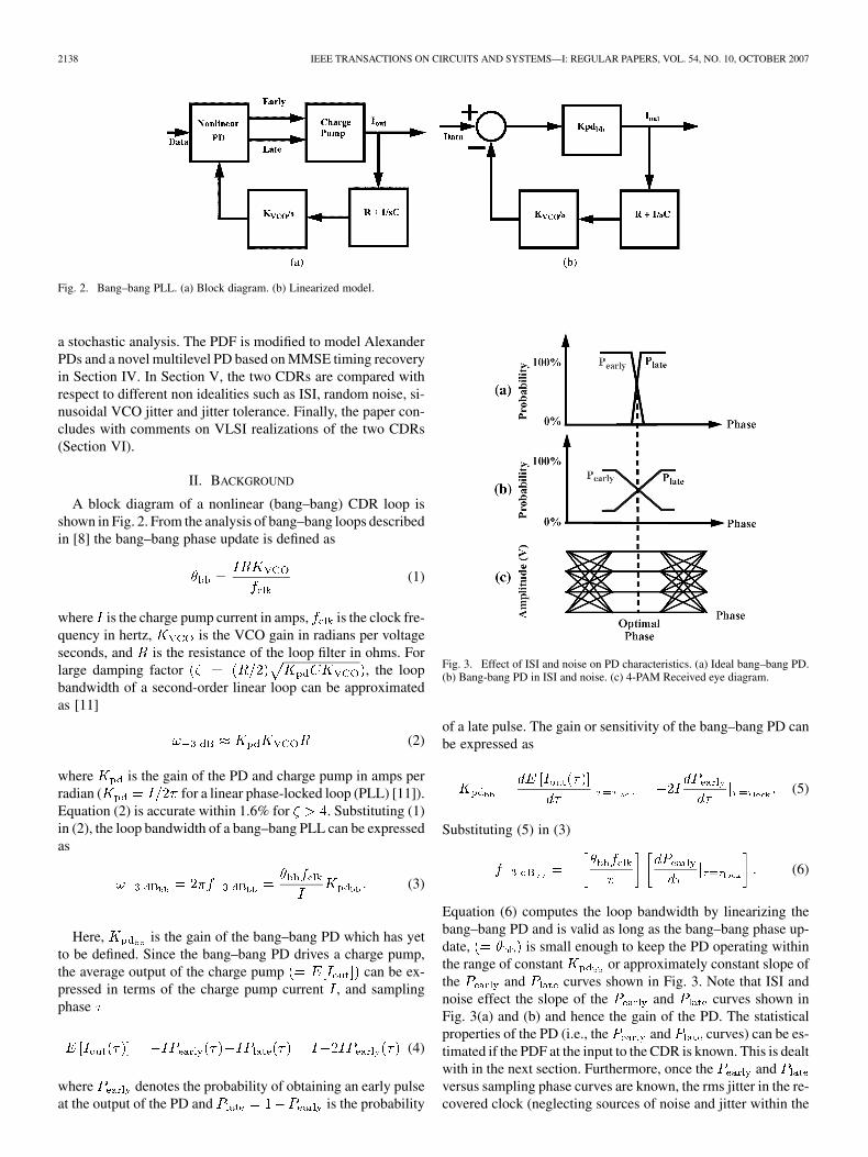
Fig. 2. Bang–bang PLL. (a) Block diagram. (b) Linearized model.
a stochastic analysis. The PDF is modified to model AlexanderPDs and a novel multilevel PD based on MMSE timing recoveryin Section IV. In Section V, the two CDRs are compared withrespect to different non idealities such as ISI, random noise, si-nusoidal VCO jitter and jitter tolerance. Finally, the paper con-cludes with comments on VLSI realizations of the two CDRs(Section VI).
II. BACKGROUND
A block diagram of a nonlinear (bang–bang) CDR loop isshown in Fig. 2. From the analysis of bang–bang loops describedin [8] the bang–bang phase update is defined as
(1)
where is the charge pump current in amps, is the clock fre-quency in hertz, is the VCO gain in radians per voltageseconds, and is the resistance of the loop filter in ohms. Forlarge damping factor , the loopbandwidth of a second-order linear loop can be approximatedas [11]
(2)
where is the gain of the PD and charge pump in amps perradian ( for a linear phase-locked loop (PLL) [11]).Equation (2) is accurate within 1.6% for . Substituting (1)in (2), the loop bandwidth of a bang–bang PLL can be expressedas
(3)
Here, is the gain of the bang–bang PD which has yetto be defined. Since the bang–bang PD drives a charge pump,the average output of the charge pump can be ex-pressed in terms of the charge pump current , and samplingphase
(4)
where denotes the probability of obtaining an early pulseat the output of the PD and is the probability
Fig. 3. Effect of ISI and noise on PD characteristics. (a) Ideal bang–bang PD.(b) Bang-bang PD in ISI and noise. (c) 4-PAM Received eye diagram.
of a late pulse. The gain or sensitivity of the bang–bang PD canbe expressed as
(5)
Substituting (5) in (3)
(6)
Equation (6) computes the loop bandwidth by linearizing thebang–bang PD and is valid as long as the bang–bang phase up-date, is small enough to keep the PD operating withinthe range of constant or approximately constant slope ofthe and curves shown in Fig. 3. Note that ISI andnoise effect the slope of the and curves shown inFig. 3(a) and (b) and hence the gain of the PD. The statisticalproperties of the PD (i.e., the and curves) can be es-timated if the PDF at the input to the CDR is known. This is dealtwith in the next section. Furthermore, once the andversus sampling phase curves are known, the rms jitter in the re-covered clock (neglecting sources of noise and jitter within the

MUSA AND CARUSONE: MODELING AND DESIGN OF MULTILEVEL BANG–BANG CDRs 2139
Fig. 4. Pulse response h of a typical serial link that consists of a coaxial cablechannel model and first-order receive filter.
loop) can be estimated following the linearized analysis in [8].The resulting rms jitter (in radians) can therefore be expressedas
(7)
Substituting (3) in (7) we get
(8)
Equation (8) relates the loop bandwidth and the statistical prop-erties of the PD to the rms jitter of the recovered clock. Notethat for a fixed-loop bandwidth, a CDR’s recovered clock jitteris inversely proportional to the slope of its versus phasecurves in the vicinity of the lock point. If the recovered clockjitter is high, the clock phase, will wander over a range forwhich the slope is no longer constant making it dif-ficult to apply (8). This variation in can be taken intoaccount by using a random walk model or Markov chain [12].In this work, both the linear model in (8) and the Markov chainwill be used to predict the rms jitter of the CDR.
III. STOCHASTIC MODELING OF CDR INPUT
The purpose of this section is to obtain an expression for thePDF of the input signal to the CDR (which is labelled as Y inFig. 1) as a function of sampling phase, , from a knowledgeof the channel response, the receiver front-end, and the additivenoise. This expression can then be used to evaluate theand curves for the bang–bang CDR and eventually the gainof the PD.
A. Effect of Channel Response
The analysis assumes that the pulse response of the channel isknown. Fig. 4 shows a typical pulse response, , of the entirepath from transmitter to the CDR input. Included in is acoaxial cable model used as the channel and a receiver front-endmodeled as a first-order low-pass filter
(9)
Fig. 5. Example of computing a sampled voltage at a particular sampling phase.(a) Transmitted symbols. (b) Received pulses (with ISI). (c) Received signal.
The input to the CDR can be expressed as
(10)
Here is the random data input to the channel and is the re-ceiver front-end output. Fig. 5 illustrates how previous symbolsinterfere with the current bit to produce the sampled voltage atany particular sampling phase. Fig. 5(a) shows a sequence oftransmitted symbols. Neglecting the channel delay, the channeloutputs a sequence of pulses, each pulse being weighted by thecorresponding transmitted symbol. This is shown in Fig. 5(b).The received signal is a sum of these pulses. Thus, at time
the receiver sampled voltage can be expressed as asum of points , , and in Fig. 5(b) where is the sample ofthe current symbol and , are samples of previous symbols.Let be the baud rate samples of for a particular samplingphase . For instance, Fig. 4 plots for two different samplingphases: and ps. Thus, can be expressed as
(11)
Substituting (11) in (10) we get
(12)
The infinite sum in (12) can be made finite by neglecting thenegligible tails of outside the range
(13)

2140 IEEE TRANSACTIONS ON CIRCUITS AND SYSTEMS—I: REGULAR PAPERS, VOL. 54, NO. 10, OCTOBER 2007
For a finite of length , there are possible se-quences of transmitted 4-PAM data: .Let be a matrix whose rows are all of thepossible transmitted 4-PAM data patterns of length and
be the element of in row and column . Hence, thechannel output corresponding to the data pattern in row ofis
(14)
Thus, for a particular sampling phase there are possiblevalues of the CDR input given by (14), each correspondingto a row of the data matrix . Assuming random uncorrelateddata, each sequence will occur with probability . Thus,the PDF for the signal (assuming no random noise) for a par-ticular sampling phase can be expressed as
(15)
Note that the data matrix can be generalized for line coding byweighting each term of the summation in (15) by the probabilityof the corresponding data pattern. Some PDs are inactive forcertain received data patterns, in which case the correspondingterms in (14) must be omitted.
B. Additive Noise
Noise in the channel and receiver front-end is modeled as anequivalent input referred noise source. If the PDF of the additivenoise is , then the PDF of the signal (Fig. 1) at the inputto the CDR for any sampling phase can be obtained by simplyconvolving and in (15)
(16)
For the special case of Gaussian noise
(17)
Substituting (17) in (16)
(18)
In essence, the PDF is a sum of Gaussian distributions. The con-stants define the means of the Gaussians in terms of thesampled pulse response (deterministic jitter). Each Gaussianhas a variance of (random jitter). Note that for evaluatingin (18), the entire pulse response from transmitter to the CDRinput has to be considered.
TABLE IPARAMETERS FOR THE SYSTEM IN FIG. 1
Fig. 6. PDF at two different sampling phases of a given data eye. (a) Eye dia-gram. (b) PDF at data transition. (c) PDF at maximum data eye opening.
C. System Level Parameters
System level parameters used for behavioral simulations areshown in Table I. The input random data sequence is assumedto be a 4-PAM system with equi-probable values at 1.5, 0.5,
0.5, and 1.5. The effect of baseline wander is neglected sincethe channel is assumed to be dc coupled. Using (18) and the pa-rameters in Table I, the PDF at the input to the CDR is calculatedfor two different sampling phases (Fig. 6). Good agreement withtime-domain simulations in Simulink is also observed. The SNRand the channel length will be varied in subsequent sections toobserve the effect of these parameters on CDR performance.
IV. MULTILEVEL CDR ARCHITECTURES
This section attempts to model Alexander PD and MMSEPD-based CDR architectures for multilevel signals using thestochastic analysis in the previous section.
A. Alexander PD-Based CDR
In the presence of data transitions, the Alexander PD [14]generates an early or late pulse depending on whether theclock leads or lags the data. A possible implementation of anAlexander PD modified for 4-PAM signals is shown in Fig. 7[4]–[7]. The input data is sampled at the rising and fallingedges of a full-rate clock. The input being a 4-PAM signal,the sampled values are sent to a bank of clocked comparators

MUSA AND CARUSONE: MODELING AND DESIGN OF MULTILEVEL BANG–BANG CDRs 2141
Fig. 7. Block diagram of 4-PAM Alexander PD [4]–[7].
to detect the correct signal level. The choice of the thresholddepends on the input data eye. The usual Alexander PD
logic is authenticated by a transition detector which filters outundesired transitions such as 1.5 to 0.5 and vice versa.The desired transition types are [7]: 1) Symmetric crossingsi.e., transitions from 1.5 to 1.5 and vice versa; 0.5 to 0.5and vice versa; 2) 1.5 to 0.5 and vice versa; 3) 1.5 to 0.5and vice versa. The PD logic is enabled through a controlsignal whenever any one of these transitions are detected. Forexample, if a transition from 1.5 to 1.5 is detected then theearly/late pulses can be generated through logic gates as
(19)
where is the current data sample output of the zerothreshold clocked comparator (Fig. 7), is the correspondingedge sample and is the data sample from the previousperiod. To determine the and versus sampling phasecurves for this PD, the statistics of the received waveform atdata transitions are required. Hence, to model the CDR in lock,the PDF of the transition edge samples is needed.
Fig. 8 shows one of the data transitions of a 4-PAM signal andtwo PDFs corresponding to different transition edge samplingphases A and B. Sampling phase A leads the zero crossing whilesampling phase B lags. For a leading sampling phase, we expect
and vice versa for a lagging sampling phase.Note that an early pulse will be generated by the PD wheneverthe sampled value at the rising data transition edge is belowthe threshold. Thus, for sampling phase A or B, the probabilityof an early pulse when the data transitions from 1.5 to 1.5
can be expressed as
(20)
Fig. 8. Example of calculating P and P for two different transitionedge samples using PDFs.
where denotes the PDF corresponding to a tran-sition from 1.5 to 1.5 in the 4-PAM signal . This PDF canbe derived from the PDF in (18) by modifying the data matrixto include only rows whose th and th columns are 1.5and 1.5, respectively. Consequently, the modified 4-PAM datamatrix will have dimensions . For example, if
the modified data matrix can be expressed as1
(21)
Thus, can be expressed as
(22)
and
(23)
Evaluating (22)
(24)
1Practically m is much larger than 2. m = 2 is chosen here to illustrate thedata transition matrix.
2142 IEEE TRANSACTIONS ON CIRCUITS AND SYSTEMS—I: REGULAR PAPERS, VOL. 54, NO. 10, OCTOBER 2007
Fig. 9. Plots ofP andP values for Alexander PD for 13.8-GHz coaxialcable channel model, SNR = 43 dB, 4 Gsymbol/s 4-PAM data, and 4-GHzreceiver front-end.
where is the complementary error function. Similarly, theprobability of a late pulse when the data transitions from 1.5to 1.5 can be expressed as
(25)
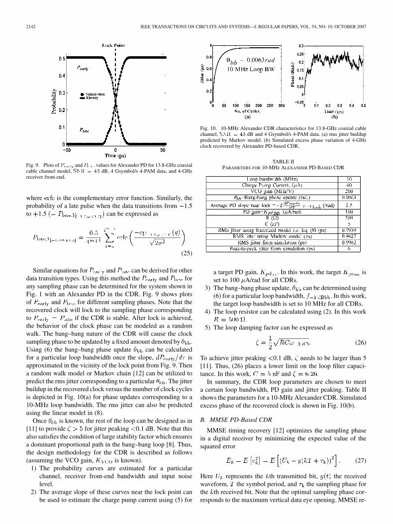
Similar equations for and can be derived for otherdata transition types. Using this method the and forany sampling phase can be determined for the system shown inFig. 1 with an Alexander PD in the CDR. Fig. 9 shows plotsof and for different sampling phases. Note that therecovered clock will lock to the sampling phase correspondingto if the CDR is stable. After lock is achieved,the behavior of the clock phase can be modeled as a randomwalk. The bang–bang nature of the CDR will cause the clocksampling phase to be updated by a fixed amount denoted by .Using (6) the bang–bang phase update can be calculatedfor a particular loop bandwidth once the slope, isapproximated in the vicinity of the lock point from Fig. 9. Thena random walk model or Markov chain [12] can be utilized topredict the rms jitter corresponding to a particular . The jitterbuildup in the recovered clock versus the number of clock cyclesis depicted in Fig. 10(a) for phase updates corresponding to a10-MHz loop bandwidth. The rms jitter can also be predictedusing the linear model in (8).
Once is known, the rest of the loop can be designed as in[11] to provide for jitter peaking 0.1 dB. Note that thisalso satisfies the condition of large stability factor which ensuresa dominant proportional path in the bang–bang loop [8]. Thus,the design methodology for the CDR is described as follows(assuming the VCO gain, is known).
1) The probability curves are estimated for a particularchannel, receiver front-end bandwidth and input noiselevel.
2) The average slope of these curves near the lock point canbe used to estimate the charge pump current using (5) for
Fig. 10. 10-MHz Alexander CDR characteristics for 13.8-GHz coaxial cablechannel, SNR = 43 dB and 4 Gsymbol/s 4-PAM data. (a) rms jitter builduppredicted by Markov model. (b) Simulated excess phase variation of 4-GHzclock recovered by Alexander PD-based CDR.
TABLE IIPARAMETERS FOR 10-MHz ALEXANDER PD-BASED CDR
a target PD gain, . In this work, the target isset to 100 A/rad for all CDRs.
3) The bang–bang phase update, can be determined using(6) for a particular loop bandwidth, . In this work,the target loop bandwidth is set to 10 MHz for all CDRs.
4) The loop resistor can be calculated using (2). In this work.
5) The loop damping factor can be expressed as
(26)
To achieve jitter peaking 0.1 dB, needs to be larger than 5[11]. Thus, (26) places a lower limit on the loop filter capaci-tance. In this work, nF and .
In summary, the CDR loop parameters are chosen to meeta certain loop bandwidth, PD gain and jitter peaking. Table IIshows the parameters for a 10-MHz Alexander CDR. Simulatedexcess phase of the recovered clock is shown in Fig. 10(b).
B. MMSE PD-Based CDR
MMSE timing recovery [12] optimizes the sampling phasein a digital receiver by minimizing the expected value of thesquared error
(27)
Here represents the th transmitted bit, the receivedwaveform, the symbol period, and the sampling phase forthe th received bit. Note that the optimal sampling phase cor-responds to the maximum vertical data eye opening. MMSE re-

MUSA AND CARUSONE: MODELING AND DESIGN OF MULTILEVEL BANG–BANG CDRs 2143
quires that the sampling phase, be adjusted in the directionopposite the gradient,
(28)
Here is a parameter that is chosen to trade-off acquisition timewith jitter and determines how quickly is adjusted. Substi-tuting (27) into (28) and dropping the expectation operator re-sults in the following stochastic gradient update rule:
(29)
Practical high-speed implementations of the LMS algorithmoften use only 1-bit representations of the sign of the error andthe slope [15]. Applying this idea to MMSE TR results in thefollowing sign–sign MMSE (SSMMSE) rule [16] :
(30)
Here, (the bang–bang phase update) replaces . In a prac-tical bang–bang CDR, a small integral term is added to the rightside of (30). Thus, to summarize, this method requires the fol-lowing two quantities: 1) the sign of the slope of the receivedsignal at the sampling instant; 2) the sign of the error betweenthe sampled value and a particular signal level. Once these sig-nals are available in binary form, early/late pulses can be gen-erated using logic gates [16]
(31)
where is the data sample corresponding to a particular signallevel. The error with respect to a particular signal level can begenerated by a comparator. This will often be required for otherpurposes as well such as adaptive equalization [17], hence noextra hardware will be necessary.
The algorithm may be simplified by eliminating the errorsignal altogether. Suppose the PD is monitoring a 1.5 level.Thus, the error signal where is the re-ceived signal. Note that will be 0 most of the time since it ishighly unlikely that the signal will rise above 1.5. This can beeasily seen in the 4-PAM eye diagram of Fig. 6(a). Setting tozero in (31) results in the following logic:
(32)
A similar modification can be made when monitoring the 1.5level. The only difference will be that the error signal in this casewill be . Therefore, the error will be 1 mostof the time. Besides hardware reduction, another advantage ofmonitoring the max. and min. signal levels is the lower jitter inthe recovered clock [16]. The main challenge in the design isimplementing a high-frequency slope detector. One possibilityis to use passive - sections as shown in Fig. 11. Therelative phase shift between the data and slope outputs will be90 over a broad bandwidth. The low-pass and high-pass filters
Fig. 11. Multilevel PAM timing recovery using an SSMMSE PD with a fullrate clock (+1.5 and �1.5 levels are being monitored).
can be realized using on chip passive components. The choiceof the filter time constant is a tradeoff between bandwidth ofreceiver front-end and sensitivity of the slope detector. For thiswork, Grad/s. As proposed in [18], an activefilter may also be used.
Note that in Fig. 11, the early/late decisions of the PD de-pend on both the signal and the derivative of the signal.Hence, for each sampling phase a PDF can be computed for thesignal and a corresponding PDF for the slope by using(18) provided that the slope detector bandwidth is included inthe pulse response of the channel. Each of these PDFs will havetheir own vectors (i.e., and ) corresponding to each pos-sible combination of data. Since the phase update depends onboth of these two signals, a joint PDF of these two signals needsto be constructed for each sampling phase. A joint PDF requiresthe calculation of the correlation-coefficient function which isgiven as [13]
(33)
However, it can be shown that this function is zero for a signaland its slope at a particular sampling phase (Appendix). Thejoint PDF of the signal and its slope for a particular sam-pling phase can be expressed as
(34)
where . Note that the noise vari-ance of the slope signal , is influenced by the derivativeand hence is different from the noise variance of the data signal
. When the SSMMSE PD is monitoring 1.5 level, theprobability that an early pulse will be generated for a particularsampling phase can be expressed as
(35)

2144 IEEE TRANSACTIONS ON CIRCUITS AND SYSTEMS—I: REGULAR PAPERS, VOL. 54, NO. 10, OCTOBER 2007
Fig. 12. SSMMSEPD characteristics for 13.8-GHz coaxial cable channelmodel, SNR = 43 dB, 4 Gsymbol/s 4-PAM data and passive slope detectorwith 10-GHz cutoff frequency. (a) Eye diagram of CDR input (i.e., signal Yin Fig. 11. (b) Simulated and theoretical P and P for SSMMSEPD.
where represents the threshold voltage of the data com-parator [Fig. 11]. Evaluating the integrals in (35)
(36)
where and denote the error and complementaryerror function, respectively and . The prob-ability of obtaining a late pulse (when monitoring 1.5 level)can be expressed as
(37)
Similar equations can be derived for early and late pulses whenmonitoring 1.5 level. Using these equations, the and
for each sampling phase can be determined for the systemshown in Fig. 1 with an SSMMSE PD in the CDR. Fig. 12 showsplots of and for all sampling phases along with theeye diagram of the received data. The rms jitter can now be de-termined using (8) and a random walk model (Markov chain) fora particular loop bandwidth. Using the design methodology de-scribed for the Alexander PD-based CDR, the SSMMSE CDR
TABLE IIIPARAMETERS FOR 10-MHz SSMMSE PD-BASED CDR
Fig. 13. 10-MHz SSMMSE PD-based CDR characteristics for 13.8-GHzcoaxial cable channel model, SNR = 43 dB, 4 Gsymbol/s 4-PAM dataand passive slope detector with 10-GHz cutoff frequency. (a) Jitter builduppredicted by Markov model. (b) Simulated excess phase variation of 4-GHzclock recovered by SSMMSE PD-based CDR.
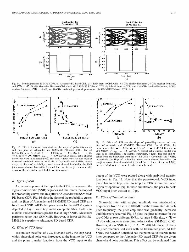
is designed for 10-MHz loop bandwidth. Table III shows theparameter values of the designed CDR. The jitter buildup pre-dicted by a Markov model is depicted in Fig. 13(a) for phaseupdates corresponding to a 10-MHz loop bandwidth. Simulatedexcess phase of the recovered clock is shown in Fig. 13(b).Fig. 14 depicts simulated eye diagrams of the data input to theCDR and the recovered clocks for Alexander PD and SSMMSEPD at 10-MHz loop bandwidth. Note that the lock point for theSSMMSE CDR corresponds to the maximum data eye opening,not the midpoint between data transitions as in the AlexanderPD.
V. EFFECT OF SYSTEM NONIDEALITIES
In this section, the effect of different nonidealities on the CDRperformance will be investigated.
A. Effect of Channel Bandwidth
Increasing the channel length reduces the bandwidth of thechannel and leads to greater ISI. This degrades the slope ofthe probability curves (Fig. 3) and results in a larger rms jitterfor a fixed-loop bandwidth (8). Fig. 15 plots the slope of theprobability curves and rms jitter of Alexander and SSMMSEPD-based CDR as a function of channel bandwidth. All Table Iparameters for the 4-PAM system depicted in Fig. 1 were keptintact except the channel length. Both simulations and calcula-tions predict that at large channel bandwidths, Alexander per-forms better than SSMMSE. However, at lower channel band-widths, SSMMSE is superior to Alexander PD-based CDR.
MUSA AND CARUSONE: MODELING AND DESIGN OF MULTILEVEL BANG–BANG CDRs 2145
Fig. 14. Eye diagrams for 10-MHz CDRs. (a) Alexander PD-based CDR. (i) 4-PAM input to CDR with 13.8-GHz bandwidth channel, 4-GHz receiver front-end,and SNR = 43 dB. (ii) Alexander PD-based CDR clock. (b) SSMMSE PD-based CDR. (i) 4-PAM input to CDR with 13.8-GHz bandwidth channel, 4-GHzreceiver front-end, SNR = 43 dB, and 10-GHz bandwidth passive slope detector. (ii) SSMMSE PD-based CDR clock.
Fig. 15. Effect of channel bandwidth on the slope of probability curvesand rms jitter of Alexander and SSMMSE PD-based CDR. For allCDRs, the loop bandwidth = 10 MHz, R = 0:5 k, C = 5 nF,VCO gain = 200 MHz/V, K = 100 �A/rad. A coaxial cable channelmodel was used in all simulations. The SNR, 4-PAM data rate and receiverfront-end bandwidth were set to 43 dB, 4 Gsymbol/s and 4 GHz, respec-tively. (a) Slope of probability curves versus channel bandwidth. (b) RMSjitter versus channel bandwidth (dashed line = linear jitter model (8);cross = Markov jitter model; dots = simulation).
B. Effect of SNR
As the noise power at the input to the CDR is increased, thesignal-to-noise ratio (SNR) degrades and this lowers the slope ofthe probability curves and rms jitter of Alexander and SSMMSEPD-based CDR. Fig. 16 plots the slope of the probability curvesand rms jitter of Alexander and SSMMSE PD-based CDR as afunction of SNR. All Table I parameters for the 4-PAM systemdepicted in Fig. 1 were kept intact except the SNR. Both sim-ulations and calculations predict that at large SNRs, Alexanderperforms better than SSMMSE. However, at lower SNRs, SS-MMSE is superior to Alexander PD-based CDR.
C. Effect of VCO Jitter
To simulate the effect of VCO jitter and verfiy the loop band-width, sinusoidal noise was introduced at the input to the VCOand the phase transfer functions from the VCO input to the
Fig. 16. Effect of SNR on the slope of probability curves and rmsjitter of Alexander and SSMMSE PD-based CDR. For all CDRs, theloop bandwidth = 10 MHz, R = 0:5 k, C = 5 nF, VCO gain =200 MHz/V, K = 100 �A/rad. A coaxial cable channel model wasused in all simulations. The channel bandwidth, 4-PAM data rate and re-ceiver front-end bandwidth were set to 13.8 GHz, 4 Gsymbol/s and 4 GHz,respectively. (a) Slope of probability curves versus channel bandwidth. (b)rms jitter versus channel bandwidth (dashed line = linear jitter model(8);cross = Markov jitter model; dots = simulation).
output of the VCO were plotted along with analytical transferfunctions in Fig. 17. Note that the peak-to-peak VCO inputphase has to be kept small to keep the CDR within the linearregion of operation [9]. In these simulations, the peak-to-peakVCO input jitter was set to 10 ps.
D. Effect of Transmitter Jitter
Sinusoidal jitter with varying amplitude was introduced atfrequencies from 50 kHz to 100 MHz at the transmitter. At eachjitter frequency, the jitter amplitude was gradually increaseduntil bit errors occurred. Fig. 18 plots the jitter tolerance for thetwo CDRs at two different SNRs. At large SNRs (i.e.,
dB) Alexander is more jitter tolerant than SSMMSE CDR.However, at low SNRs (i.e., dB) Alexander PD failsthe jitter tolerance test even with no transmitter jitter. At lowSNRs, the SSMMSE method has the potential to tolerate morejitter compared to the Alexander PD-based CDR for the givenchannel and noise conditions. This effect can be explained from

2146 IEEE TRANSACTIONS ON CIRCUITS AND SYSTEMS—I: REGULAR PAPERS, VOL. 54, NO. 10, OCTOBER 2007
Fig. 17. CDR transfer characteristics with 13.8-GHz coaxial cable channel,SNR = 43 dB, 4 Gsymbol/s 4-PAM data and 4-GHz receiver front-end(solid line, linearized analysis; dots, simulation results for SSMMSE PD-basedCDR; cross, simulation results for Alexander PD-based CDR. For allCDRs, the loop bandwidth = 10 MHz, R = 0:5 k, C = 5 nF,VCO gain = 200 MHz/V, K = 100 �A/rad.
Fig. 18. CDR jitter tolerance simulation results with 13.8-GHz bandwidthcoaxial cable channel, 4 Gsymbol/s and 4-GHz receiver front-end. For allCDRs, the loop bandwidth = 10 MHz, R = 0:5 k, C = 5 nF,VCO gain = 200 MHz/V, K = 100 �A/rad.
the input eye diagrams shown in Fig. 19 for two different SNRs.At low SNRs, the data transitions are more effected by noise,than the peak in the eye opening. Since the SSMMSE techniquetracks the maximum data eye opening instead of the data tran-sitions, it has better jitter tolerance compared to the AlexanderPD-based CDR at low SNRs.
VI. CONCLUSION
Analysis and design of multilevel bang–bang CDRs were pre-sented. A sampling-phase-dependent PDF is derived and uti-lized to model two different bang–bang CDRs: Alexander andSSMMSE. The CDRs are modeled by calculating the slope ofthe and versus sampling phase curves in the vicinityof the lock point. The loop bandwidth of the CDR is directlyproportional to the slope of the and curves in thevicinity of the lock point. A CDR with a lower slope will re-quire a larger charge pump current and a larger bang–bang phasestep to meet a target loop bandwidth. Therefore, the slope of the
and curves is an important performance metric ofany bang–bang CDR. A steeper slope implies lower rms jitterand higher jitter tolerance. Since the CDR input statistics effectthe PD gain the choice of the best PD will in general depend on
the channel ISI and noise. The analysis presented here is par-ticularly well suited to multilevel systems where ISI and noisebecome important due to the degradation in voltage margin as aresult of the increased number of levels.
Analysis showed that for the coaxial cable channel andGaussian noise conditions assumed, the SSMMSE PD per-formed better compared to the Alexander PD at large ISI andlow SNRs since the SSMMSE PD maintained a higher slopeof the and curves. At large ISI and low SNRs, thenoise in the data transitions is effectively worse than in themaximum data eye opening; thus causing the SSMMSE PD toperform better than the Alexander PD-based CDR under theseconditions.
Comparison of the hardware requirements of the two CDRsis given in Table IV. The SSMMSE method presented in thiswork is hardware efficient compared to an Alexander PD-basedCDR. A particularly important feature of the SSMMSE methodis that it requires half the number of clock sampling phases asthat of the Alexander PD. For example, to retime the data witha quarter rate clock, an Alexander PD would require eight clockphases separated in phase by 45 but the SSMMSE method re-quires only four clock phases separated in phase by 90 . Thus,the SSMMSE method would require a simpler and lower powerVCO.
APPENDIX
CORRELATION-COEFFICIENT FUNCTION FOR SSMMSE PD
The purpose of this section is to prove that the correlation-coefficient function for a random signal and its slope,
is equal to zero. From (33)
(38)
For uncorrelated random data, . Also, where denotes the cross correlation between
and for a lag (or delay) of zero. Therefore
(39)
If is a wide-sense stationary process, then its cross-correla-tion with its slope can be expressed as [13]
(40)
where is the delay (or lag) between the signal and its slope,and is the auto-correlation function for the signal
for a delay of . Substituting (40) in (39)
(41)
is expressed as [13]
(42)

MUSA AND CARUSONE: MODELING AND DESIGN OF MULTILEVEL BANG–BANG CDRs 2147
Fig. 19. Eye diagram of 4 Gsymbol/s, 4-PAM data with 13.8-GHz channel. (a) SNR = 43 dB. (b) SNR = 28 dB.
TABLE IVCOMPARISON OF THE HARDWARE REQUIREMENTS OF
ALEXANDER PD AND SSMMSE PD
where denotes the power-spectral density of . Sub-stituting (42) in (41) and simplifying
(43)
REFERENCES
[1] C.-K. K. Yang, R. Farjad-Rad, and M. Horowitz, “A 0.6 �m CMOS 4Gb/s transceiver with data recovery using oversampling,” in Dig. Tech.Papers 1997 Symp. VLSI Circuits , Jun. 1997, pp. 71–72.
[2] J. Savoj and B. Razavi, “A 10 Gb/s CMOS clock-and-data recoverycircuit with a half rate binary phase/frequency detector,” IEEE J. Solid-State Circuits, vol. 38, no. 1, pp. 1135–1145, Jan. 2003.
[3] J. Rogers and J. Long, “A 10 Gb/s CDR/DEMUX with LC delay lineVCO in 0.18 m CMOS,” in Dig. Tech. Papers 2002 IEEE Int. Solid-State Circuits Conf., Feb. 2002, vol. 1, pp. 3–7.
[4] J. Stonick, G. Wei, J. Sonntag, and D. Weinlader, “An adaptive PAM-45 Gb/s backplane transceiver in 0.25-�m CMOS,” IEEE J. Solid-StateCircuits, vol. 38, no. 3, pp. 436–443, Mar. 2003.
[5] R. Farjad-Rad, C. Yang, M. Horowitz, and T. H. Lee, “A 0.3�m CMOS8-Gb/s 4-PAM serial link transceiver,” IEEE J. Solid-State Circuits, vol.35, no. 5, pp. 757–764, May 2000.
[6] J. L. Zerbe, C. W. Werner, V. Stojanovic, F. Chen, J. Wei, G. Tsang,W. Stonecypher, A. Ho, T. P. Thrush, R. T. Kollipara, M. A. Horowitz,and K. S. Donelly, “Equalization and clock recovery for a 2.5 Gb/s–10Gb/s 2-PAM/4-PAM backplane transceiver cell,” IEEE J. Solid-StateCircuits, vol. 38, no. 12, pp. 2121–2130, Dec. 2003.
[7] T. Toifl et al., “A 22-Gb/s PAM-4 receiver in 90-nm CMOS SOI tech-nology,” IEEE J. Solid-State Circuits, vol. 41, no. 4, pp. 954–965, Apr.2006.
[8] R. Walker, “Designing bang–bang PLLs for clock-and-data recoveryin serial data transmission systems,” in Phase Locking in High Perfor-mance Systems. New York: IEEE Press, 2003, pp. 34–45.
[9] J. Lee, K. Kundert, and B. Razavi, “Modeling of jitter in bang–bangclock-and-data recovery circuits,” in Proc. 2003 Custom Integr. Cir-cuits Conf., Sep. 2003, pp. 711–714.
[10] V. Stojanovic and M. Horowitz, “Modeling and analysis of high-speedlinks,” in Proc. 2003 Custom Integrated Circuits Conference, Sep.2003, pp. 589–594.
[11] B. Razavi, Design of Integrated Circuits for Optical Communica-tions. New York: McGraw Hill, Sep. 2002.
[12] E. Lee and D. Messerschmitt, Digital Communication, 2nd ed. Nor-well, MA: Kluwer , 1997.
[13] A. Leon-Garcia, Probability and Random Processes for Electrical En-gineering, 2nd ed. Reading, MA: Addison-Wesley, 1994.
[14] J. Alexander, “Clock recovery from random binary signals,” Electron.Lett., vol. 111, pp. 541–542, Oct. 1975.
[15] M. Le, P. Hurst, and J. Keane, “An adaptive analog noise-predictivedecision-feedback equalizer,” IEEE J. Solid State Circuits, vol. 37, no.2, pp. 105–113, Feb. 2002.
[16] F. Musa and A. C. Carusone, “Clock recovery in high-speed multilevelserial links,” in Proc. 2003 Int. Symp. Circuits Syst., May 2003, pp.449–452.
[17] V. Balan et al., “A 4.8–6.4-Gb/s serial link for backplane applicationsusing decision feedback equalization,” IEEE J. Solid State Circuits, vol.40, no. 9, pp. 1957–1967, Sep. 2005.
[18] F. Musa and A. C. Carusone, “A baud-rate timing recovery schemewith a dual-function analog filter,” IEEE Trans. Circuits Syst. II, Exp.Briefs, vol. 53, no. 12, pp. 1393–1397, Dec. 2006.
Faisal Ahmed Musa (S’01) received the B.Sc.degree from Bangladesh University of Engineeringand Technology (BUET), Dhaka, Bangladesh, in2000, and the M.S. degree from the University ofConnecticut, Storrs, in 2001, both in electrical en-gineering. He is currently working toward the Ph.D.degree at the University of Toronto, Toronto, ON,Canada.
During the summer of 2004, he worked on thedesign of high-speed clock recovery systems atIntel’s Microprocessor Technology Laboratory,
Hillsboro, OR. Since November 2006, he has also been working at GennumCorporation on the design and verification of high-speed phase-locked loops(PLLs). His research interests include modeling, design and implementation ofhigh-speed chip-to-chip signaling interfaces.
Mr. Musa was named an Edward S. Rogers Scholar by the Faculty of Engi-neering at the University of Toronto in both 2004 and 2005.
Anthony Chan Carusone (S’96–M’02) receivedthe B.A.Sc. and Ph.D. degrees from the Universityof Toronto, Toronto, ON, Canada, in 1997 and 2002,respectively.
Since 2001, he has been with the University ofToronto, where he is currently and Associate Pro-fessor in the Department of Electrical and ComputerEngineering,
Dr. Carusone was named an Ontario Distin-guished Researcher in 2002. Since then, he has heldthe Canada Research Chair in Integrated Systems.
During his doctoral study, he received the Governor-General’s Silver Medal.He was a coauthor of the best paper at the 2005 Compound SemiconductorIntegrated Circuits Symposium. He is Past Chair of the Analog Signal Pro-cessing Technical Committee for the IEEE Circuits and Systems Society, amember of the technical program committee for the Custom Integrated CircuitsConference, and an Associate Editor of the IEEE TRANSACTIONS ON CIRCUITS
AND SYSTEMS—II: EXPRESS BRIEFS.