IEEE Std 1050-2004 IEEE Guide for Instrumentation and Control Equipment Grounding in Generating...
101
IEEE Std 1050 ™ -2004 (Revision of IEEE Std 1050-1996) 1050 TM IEEE Guide for Instrumentation and Control Equipment Grounding in Generating Stations 3 Park Avenue, New York, NY10016-5997, USA IEEE Power Engineering Society Sponsored by the Energy Development and Power Generation Committee 14 September 2005 Print: SH95270 PDF: SS95270
description
Instrumentation
Transcript of IEEE Std 1050-2004 IEEE Guide for Instrumentation and Control Equipment Grounding in Generating...
IEEE Std 1050™-2004(Revision of
IEEE Std 1050-1996)
1050TM
IEEE Guide for Instrumentation andControl Equipment Grounding inGenerating Stations
3 Park Avenue, New York, NY10016-5997, USA
IEEE Power Engineering Society
Sponsored by theEnergy Development and Power Generation Committee
14 September 2005
Print: SH95270PDF: SS95270

Recognized as anAmerican National Standard (ANSI)
The Institute of Electrical and Electronics Engineers, Inc.3 Park Avenue, New York, NY 10016-5997, USA
Copyright © 2005 by the Institute of Electrical and Electronics Engineers, Inc.All rights reserved. Published 14 September 2005. Printed in the United States of America.
IEEE is a registered trademark in the U.S. Patent & Trademark Office, owned by the Institute of Electrical and ElectronicsEngineers, Incorporated.
National Electrical Code and NEC are both registered trademarks in the U.S. Patent & Trademark Office, owned by theNational Fire Protection Association, Incorporated.
National Electrical Safety Code and the NESC are both registered trademarks and service marks n the U.S. Patent &Trademark Office, owned by the Institute of Electrical and Electronics Engineers, Incorporated.
Print: ISBN 0-7381-4470-3 SH95270PDF: ISBN 0-7381-4471-1 SS95270
No part of this publication may be reproduced in any form, in an electronic retrieval system or otherwise, without the priorwritten permission of the publisher.
IEEE Std 1050
™
-2004
(Revision ofIEEE Std 1050-1996)
IEEE Guide for Instrumentation and Control Equipment Grounding in Generating Stations
Sponsor
Energy Development and Power Generation
Committee
of the
IEEE Power Engineering Society
Approved 5 February 2005
American National Standard Institute
Approved 24 September 2004
IEEE-SA Standards Board
Abstract:
Instrumentation and control (I&C) equipment grounding methods to achieve both a suit-able level of protection for personnel and equipment, and suitable electric noise immunity for signalground references in generating stations are identified.
Keywords:
control, generating stations, grounding, I&C, instrumentation
IEEE Standards
documents are developed within the IEEE Societies and the Standards Coordinating Committees of theIEEE Standards Association (IEEE-SA) Standards Board. The IEEE develops its standards through a consensusdevelopment process, approved by the American National Standards Institute, which brings together volunteersrepresenting varied viewpoints and interests to achieve the final product. Volunteers are not necessarily members of theInstitute and serve without compensation. While the IEEE administers the process and establishes rules to promote fairnessin the consensus development process, the IEEE does not independently evaluate, test, or verify the accuracy of any of theinformation contained in its standards.
Use of an IEEE Standard is wholly voluntary. The IEEE disclaims liability for any personal injury, property or otherdamage, of any nature whatsoever, whether special, indirect, consequential, or compensatory, directly or indirectly resultingfrom the publication, use of, or reliance upon this, or any other IEEE Standard document.
The IEEE does not warrant or represent the accuracy or content of the material contained herein, and expressly disclaimsany express or implied warranty, including any implied warranty of merchantability or fitness for a specific purpose, or thatthe use of the material contained herein is free from patent infringement. IEEE Standards documents are supplied “
AS IS
.”
The existence of an IEEE Standard does not imply that there are no other ways to produce, test, measure, purchase, market,or provide other goods and services related to the scope of the IEEE Standard. Furthermore, the viewpoint expressed at thetime a standard is approved and issued is subject to change brought about through developments in the state of the art andcomments received from users of the standard. Every IEEE Standard is subjected to review at least every five years forrevision or reaffirmation. When a document is more than five years old and has not been reaffirmed, it is reasonable toconclude that its contents, although still of some value, do not wholly reflect the present state of the art. Users are cautionedto check to determine that they have the latest edition of any IEEE Standard.
In publishing and making this document available, the IEEE is not suggesting or rendering professional or other servicesfor, or on behalf of, any person or entity. Nor is the IEEE undertaking to perform any duty owed by any other person orentity to another. Any person utilizing this, and any other IEEE Standards document, should rely upon the advice of a com-petent professional in determining the exercise of reasonable care in any given circumstances.
I
nterpretations: Occasionally questions may arise regarding the meaning of portions of standards as they relate to specificapplications. When the need for interpretations is brought to the attention of IEEE, the Institute will initiate action to prepareappropriate responses. Since IEEE Standards represent a consensus of concerned interests, it is important to ensure that anyinterpretation has also received the concurrence of a balance of interests. For this reason, IEEE and the members of itssocieties and Standards Coordinating Committees are not able to provide an instant response to interpretation requests exceptin those cases where the matter has previously received formal consideration. At lectures, symposia, seminars, or educationalcourses, an individual presenting information on IEEE standards shall make it clear that his or her views should be consideredthe personal views of that individual rather than the formal position, explanation, or interpretation of the IEEE.
Comments for revision of IEEE Standards are welcome from any interested party, regardless of membership affiliation withIEEE. Suggestions for changes in documents should be in the form of a proposed change of text, together with appropriatesupporting comments. Comments on standards and requests for interpretations should be addressed to:
Secretary, IEEE-SA Standards Board
445 Hoes Lane
Piscataway, NJ 08854
USA
Authorization to photocopy portions of any individual standard for internal or personal use is granted by the Institute ofElectrical and Electronics Engineers, Inc., provided that the appropriate fee is paid to Copyright Clearance Center. Toarrange for payment of licensing fee, please contact Copyright Clearance Center, Customer Service, 222 Rosewood Drive,Danvers, MA 01923 USA; +1 978 750 8400. Permission to photocopy portions of any individual standard for educationalclassroom use can also be obtained through the Copyright Clearance Center.
NOTE−Attention is called to the possibility that implementation of this standard may require use of subjectmatter covered by patent rights. By publication of this standard, no position is taken with respect to the exist-ence or validity of any patent rights in connection therewith. The IEEE shall not be responsible for identifyingpatents for which a license may be required by an IEEE standard or for conducting inquiries into the legal valid-ity or scope of those patents that are brought to its attention.
Copyright © 2005 IEEE. All rights reserved.
iii
Introduction
The original version of IEEE Std 1050 was published in 1989 after a five year development cycle. Specificrecommendations for the grounding of distributed control systems (DCS) were intentionally omitted fromthe 1989 edition since at the time the document was being written (1984–1987) there was not a large base ofinstalled systems and user experience on which to write a guide. Experience since 1989 has shown that DCSgrounding is essentially no different from the concepts presented in the 1989 version, and would not requirea specialized treatment in the guide.
The 1996 revision consisted of three major changes to the document. The first was the incorporation ofcomments, corrections, and clarifications that have been brought to the attention of the working group. Thesecond change was a significant rearrangement of the document for enhanced user-friendliness. Thisincluded a complete redrawing of the significant figures in Clause 5 to more clearly depict the conceptsbeing illustrated. The third change was the reformatting of the document to conform to the latest style man-ual for IEEE standards.
The revision includes major improvements in terminology consistency along with further elaboration of thevarious concepts that are introduced. Additional enhancements have been made to Clause 5 and its figuresfor clarity, including new subclauses on power source grounding and surge protection. Clause 6 on cableshields receives another reformatting to make the topics directly relate to the various types of I&C circuitsencountered in generating station design. Results of industry surveys are included to illustrate the prevalenceof various cable shield grounding techniques.
This guide was prepared by a Task Force of the Grounding Practices Working Group. The Working Groupis part of the Station Design, Operation, and Control Subcommittee and was sponsored by the Energy Devel-opment and Power Generation Committee of the IEEE Power Engineering Society.
Notice to users
Errata
Errata, if any, for this and all other standards can be accessed at the following URL: http://standards.ieee.org/reading/ieee/updates/errata/index.html. Users are encouraged to check this URL forerrata periodically.
Interpretations
Current interpretations can be accessed at the following URL: http://standards.ieee.org/reading/ieee/interp/index.html.
Patents
Attention is called to the possibility that implementation of this standard may require use of subject mattercovered by patent rights. By publication of this standard, no position is taken with respect to the existence orvalidity of any patent rights in connection therewith. The IEEE shall not be responsible for identifyingpatents or patent applications for which a license may be required to implement an IEEE standard or forconducting inquiries into the legal validity or scope of those patents that are brought to its attention.
This introduction in not part of IEEE Std 1050-2004, IEEE Guide for Instrumentation and Control Equip-ment Grounding in Generating Stations.
iv
Copyright © 2005 IEEE. All rights reserved.
Participants
At the time the document was approved the members of the Task Force were as follows:
Joseph R. Jancauskas,
Chair
Bruce W. Crowly,
Secretary
The following members of the individual balloting committee voted on this standard. Balloters may havevoted for approval, disapproval, or abstention.
When the IEEE-SA Standards Board approved this standard on 24 September 2004, it had the followingmembership:
Don Wright,
Chair
Steve M. Mills,
Vice Chair
Judith Gorman,
Secretary
*Member Emeritus
Also included are the following nonvoting IEEE-SA Standards Board liaisons:
Satish K. Aggarwal,
NRC Representative
Richard DeBlasio,
DOE Representative
Alan Cookson,
NIST Representative
Savoula Amanitidis
IEEE Standards Project Editor
Peter AouadAldean BengeLeslie A. D. Grant
Warren L. LewisRichard Meininger
Derek M. SawyerMalcolm V. Thaden, Jr.Gerald L. Vaughn
William AckermanSteven BrockschinkTommy CooperJoseph DeckmanWilliam G. FosseyRandall GrovesAjit Hiranandani
Edward Horgan Jr.Yuri KhersonskyLisardo LouridoGregory LuriThomas McCaffreyJames MichalecGary Michel
Charles MorsePaul PillitteriJames RuggieriMalcolm V. ThadenShanmugan ThamilarasanZhenxue XuJohn Yale
Chuck AdamsStephen BergerMark D. BowmanJoseph A. BruderBob DavisRoberto de Marca BoissonJulian Forster*Arnold M. GreenspanMark S. Halpin
Raymond HapemanRichard J. HollemanRichard H. HulettLowell G. JohnsonJoseph L. Koepfinger*Hermann KochThomas J. McGean
Daleep C. MohlaPaul NikolichT. W. OlsenRonald C. PetersenGary S. RobinsonFrank StoneMalcolm V. ThadenDoug ToppingJoe D. Watson
标准分享网 www.bzfxw.com 免费下载
Copyright © 2005 IEEE. All rights reserved.
v
Contents
1. Overview.............................................................................................................................................. 1
1.1 Scope............................................................................................................................................ 11.2 Purpose......................................................................................................................................... 1
2. Normative references ........................................................................................................................... 2
3. Definitions and acronyms .................................................................................................................... 3
3.1 Definitions.................................................................................................................................... 33.2 Acronyms..................................................................................................................................... 5
4. Design considerations for electrical noise minimization ..................................................................... 6
4.1 Typical noise sources and their characteristics............................................................................ 64.2 Noise-coupling methods ............................................................................................................ 184.3 Techniques for electrical noise minimization ............................................................................ 24
5. I&C system grounding....................................................................................................................... 41
5.1 Grounding philosophy ............................................................................................................... 415.2 Types of signal ground systems................................................................................................. 425.3 Separation criteria for circuits.................................................................................................... 485.4 I&C system power considerations ............................................................................................. 495.5 Surge protection considerations................................................................................................. 495.6 Other grounding considerations................................................................................................. 505.7 Generating station EMI environment......................................................................................... 52
6. Signal cable shield grounding............................................................................................................ 53
6.1 Cable shield requirements.......................................................................................................... 536.2 Analysis of shield grounding practices ...................................................................................... 536.3 Other cable shielding considerations ......................................................................................... 656.4 Comparison of cable shielding effectiveness............................................................................. 676.5 Common practices in shielding cables for distributed control and programmable logic
controller circuits ....................................................................................................................... 686.6 Central distribution frame (CDF) grounding practice ............................................................... 70
7. Testing................................................................................................................................................ 71
7.1 General....................................................................................................................................... 717.2 Sources of galvanic (conductive) ground loops......................................................................... 727.3 Galvanic ground loop prevention and detection ........................................................................ 727.4 Testing for ground loops............................................................................................................ 737.5 Signal ground system integrity .................................................................................................. 757.6 Maintenance of the signal ground system.................................................................................. 75
Annex A (informative) Bibliography............................................................................................................. 76
Annex B (informative) Conformance with local safety codes....................................................................... 79
Annex C (informative) Examples of I&C grounding methods...................................................................... 80

标准分享网 www.bzfxw.com 免费下载
IEEE Guide for Instrumentation and Control Equipment Grounding in Generating Stations
1. Overview
1.1 Scope
This application guide was developed to identify instrumentation and control (I&C) equipment groundingmethods to achieve both a suitable level of protection for personnel and equipment, and suitable electricnoise immunity for signal ground references in generating stations. Both ideal theoretical methods andaccepted practices in the electric utility industry are presented.
This guide is intended to give information on grounding methods for generating station instrumentation andcontrol equipment. Grounding design is normally based on the concept of two separate grounding systems,the equipment ground and the signal reference ground. The concepts of equipment grounding are well cov-ered in other IEEE standards. The concepts of grounding of instrument chassis, cable shields, signal pairs,and other related instrumentation and control items require special care in order to ensure that both person-nel working on equipment are adequately protected from electrical shock and that interference signals arenot inadvertently coupled into signal circuits. Although safety takes top priority, the I&C systems must besimultaneously safe and operationally reliable.
The basic theory and guidelines that should be understood before designing I&C grounding are presented inClause 4. Clause 5 presents various approaches for the grounding of equipment associated with generatingstation I&C systems. Clause 6 presents accepted practices in grounding the shields of I&C cables, whileClause 7 covers the testing of I&C grounding systems.
1.2 Purpose
The typical environment in a generating station provides many sources of electrical noise such as the switch-ing of large inductive loads, high fault currents, electronic drives, and high-energy, high-frequency tran-sients associated with switching at transmission voltage levels. The increasing use of solid-state equipmentand microprocessor-based control systems in these applications introduces a number of specific concernswith respect to electrical noise control. This document is a guide that discusses methods for the grounding ofinstrumentation and control equipment and their associated circuits in this environment.
Copyright © 2005 IEEE. All rights reserved. 1
IEEEStd1050-2004 IEEE GUIDE FOR INSTRUMENTATION AND
The generally low-level electrical signals transmitted from various I&C equipment in a generating stationthrough often lengthy cables may undergo signal distortion as they travel to the receiving end. This distor-tion is typically caused by noise pickup either at the signal source or along the cable run. The level of noiseon the received signal may cause operational errors and in extreme cases, damage to equipment which inturn may result in costly unit downtime. The use of proper grounding and shielding techniques can prevent alarge percentage of noise problems. It should be recognized that there are numerous accepted groundingtechniques and that the actual installation of a ground system should be made with reference to the recom-mendations of the I&C equipment manufacturers since the techniques used to solve one problem may resultin the creation of a different problem.
The grounding methods in this guide are intended to minimize degradation of instrumentation and controlsignals in generating stations. By contrast, the overall station grounding system is designed for safety con-siderations to establish a grounding system that will provide a low-impedance path for power currents toreturn to the power reference ground point for rapid fault clearing and to minimize potential differencesbetween electrical equipment and the local equipment grounding structures. The equipment grounding sys-tem is intended to reasonably ensure that hazardous voltages are not developed between grounded equip-ment or structures as a consequence of lightning surges, electrical faults, leakage or circulating currents, orstatic charges.
2. Normative references
This guide should be used in conjunction with the following standards publications. When the followingstandards are superseded by an approved revision, the revision applies.
Accredited Standards Committee C2-2002, National Electrical Safety Code® (NESC®).1
IEC/TS 61312-1:1995, Protection Against Lightning Electromagnetic Pulse (LEMP) Part I: GeneralPrinciples.2
IEEE Std C57.13.3™-1983 (Reaff 1990), IEEE Guide for the Grounding of Instrument Transformer Second-ary Circuits and Cases.3, 4
IEEE Std C62.23™-1995, IEEE Recommended Practice on Surge voltages in Low-Voltage AC PowerCircuits.
IEEE Std C62.43™-1999 IEEE Guide for the Application of Surge Protectors Used in Low-Voltage (LessThan or Equal to 1000 Vrms or 1200 Vdc) Data, Communication, and/or Signaling Circuit Application.
IEEE Std 142™-1991, IEEE Recommended Practice for Grounding of Industrial and Commercial PowerSystems (The Green Book).
IEEE Std 422™-1986, IEEE Guide for the Design and Installation of Cable Systems in Power GeneratingStations.
1The NESC is available from the Institute of Electrical and Electronics Engineers, Inc., 445 Hoes Lane, Piscataway, NJ 08854, USA(http://standards.ieee.org/).2IEC publications are available from the Sales Department of the International Electrotechnical Commission, Case Postale 131, 3, ruede Varembé, CH-1211, Genève 20, Switzerland/Suisse (http://www.iec.ch/). IEC publications are also available in the United Statesfrom the Sales Department, American National Standards Institute, 25 West 43rd Street, 4th Floor, New York, NY 10036, USA (http://www.ansi.org/).3IEEE publications are available from the Institute of Electrical and Electronics Engineers, Inc., 445 Hoes Lane, Piscataway, NJ 08854,USA (http://standards.ieee.org/).4The IEEE standards or products referred to in this clause are trademarks of the Institute of Electrical and Electronics Engineers, Inc.
2 Copyright © 2005 IEEE. All rights reserved.
标准分享网 www.bzfxw.com 免费下载
IEEE
CONTROL EQUIPMENT GROUNDING IN GENERATING STATIONS Std 1050-2004
IEEE Std 518™-1982 (Reaff 1996), IEEE Guide for the Installation of Electrical Equipment to MinimizeNoise Inputs to Controllers from External Sources.
IEEE Std 525™-1992 (Reaff 1999), IEEE Guide for the Design and Installation of Cable Systems in Substa-tions.
IEEE Std 665™-1995, IEEE Guide for Generating Station Grounding.
IEEE Std 1100™-1999, IEEE Recommended Practice for Grounding Electronic Equipment (IEEE EmeraldBook).
NFPA 70-2002: National Electrical Code® (NEC®).5
NFPA-780-2004: Standard for the Installation of Lightning Protection Systems.
3. Definitions and acronyms
3.1 Definitions
This subclause contains key terms as they are used in this guide. An asterisk (*) denotes definitions notincluded in The Authoritative Dictionary of IEEE Standards Terms [B21].6
3.2 attenuation: A general term used to denote a decrease in signal magnitude in transmission from onepoint to another.
3.3 central distribution frame grounding: A type of grounding system where all signal grounds arereferenced to a central point rather than at their respective signal sources. For certain systems this techniqueprovides a good functional compromise between the ideal signal grounding methods and ease of installationand troubleshooting.
3.4 common-mode (CM) noise: The generally unwanted noise voltage and current that appears equally andin phase from each victim signal, control, or power circuit conductor to ground, or between grounds orgrounding conductors. CM noise is also referred to as longitudinal-mode (LM) noise. Common-mode noisemay be caused by one or more of the following:
a) Electrostatic induction (E-field capacitive coupling) via near field effects. With equal capacitancebetween the set of victim conductors and their immediate surroundings, the noise voltage and cur-rent developed will be the same on all victim wires in the same circuit.
b) Magnetic induction (H-field transformer coupling) via near field effects. With the magnetic fieldlinking the set of victim conductors equally, the noise voltage and current developed will be thesame on all victim conductors in the same circuit.
c) Electromagnetic wave coupling via far-field effects. Electric dipole (or monopole) antennas and/ormagnetic loop antennas inadvertently formed in the victim conductor system can accept electromag-netic wave radiation and cause it to appear as common-mode noise and current on their path.
d) A variation in potential between two or more ground references to which the victim circuit’s con-ductors are connected. An example would be two separate buildings with a metallic signal or powercable routed between them along with a grounded circuit or signal conductor. When a lightning
5The NEC is published by the National Fire Protection Association, Batterymarch Park, Quincy, MA 02269, USA (http://www.nfpa.org). Copies are also available from the Institute of Electrical and Electronics Engineers, Inc., 445 Hoes Lane, Piscataway, NJ 08854, USA (http://standards.ieee.org/).6The numbers in brackets correspond to those of the bibliography in Annex A.
Copyright © 2005 IEEE. All rights reserved. 3
IEEEStd1050-2004 IEEE GUIDE FOR INSTRUMENTATION AND
strike or ac system ground-fault occurs at one building a CM noise condition will be produced on allof the conductors of the interconnecting cable. A potential difference is then seen to exist for theduration of the event between the two buildings via the interconnecting cable and a CM currentflows between the buildings via the cable. Note that the lightning or fault current that is coupled intothe enclosed loop area of the circuit conductors can also produce a CM effect. Direct lightning orfault current contact with the circuit conductors is not required.
3.5 coupling: The mechanism by which a near-field interference source of voltage, current, or both producesdirectly related interference in a victim circuit without a conductive (galvanic) path being involved in thetransfer. In general, coupling occurs via stray or parasitic reactive coupling means. (See: radiation in TheAuthoritative Dictionary [B21] for similar far-field effects.)
3.6 crosstalk: The unwanted transfer of signals or electrical noise by near-field coupling mechanismsbetween electrically separated, but physically adjacent circuit conductors. Crosstalk problems generally varyinversely with the spacing between the involved circuit conductors, and is commonly used in reference toeffects within multi-conductor cables.
3.7 cutoff frequency: a) (General) The frequency that is usually identified with the first –3 dB transitionbetween a passband and an adjacent attenuation band of system or transducer. b) (Of a waveguide) For agiven transmission mode in a nondissipative waveguide, the frequency at which the propagation constant is0.
3.8 distributed control system (DCS):* A control system composed of distributed software, hardware,cabling, sensors, activators, and input/output communication capability that is used to control and monitorequipment and processes.
3.9 electromagnetic compatibility (EMC):* The capability of electronic equipment or systems to be oper-ated in the intended operational electromagnetic environment at designed levels of efficiency in all designoperating modes. Also, the required ability of items of electrical and electronic equipment to be reliablyoperated without electrical interference occurring between them.
3.10 electromagnetic interference (EMI):* Impairment of a wanted electromagnetic signal by an electro-magnetic disturbance. Also, applied to equipment whose operation is impaired by conducted, coupled, orradiated electrical interference (EMI) of some type
3.11 equipment (safety) ground:* All of the conductive, normally non-current carrying metal parts ofequipment, raceways, and other enclosures that are connected to a site’s: (1) grounded ac system conductor(the neutral), (2) the related equipment grounding conductors, (3) the related ac grounding electrode conduc-tor and, (4) the related ac system earth grounding electrode itself.
3.12 ground: A conducting connection, whether intentional or accidental, between and electrical circuit orequipment and the earth or to some conducting body that serves in place of the earth (such as a vehicle’sframe).
3.13 ground, ac system: The single point at which an ac power system has its common or neutral terminalconnected to the power system ground reference.
3.14 immunity: The desirable property of equipment that prevents unintentional operation by a definedintensity of EMI.
3.15 neutral:* The terminal of a single or polyphase electrical power source that carries only the unbal-anced or triplen harmonic currents between the connected loads and the power source. On a two-wire,single-phase power source, the term “neutral” is also applied to the common terminal of the ac system. Thisterm is also applied to the circuit conductor(s) that is connected to the power source’s neutral terminal. The
4 Copyright © 2005 IEEE. All rights reserved.
标准分享网 www.bzfxw.com 免费下载
IEEE
CONTROL EQUIPMENT GROUNDING IN GENERATING STATIONS Std 1050-2004
neutral may be either solidly grounded, resistance grounded, impedance grounded, or ungrounded depend-ing upon the design requirements for the ac system.
3.16 noise (electrical): Any unwanted voltages or currents appearing in a circuit that may or may not simul-taneously contain desired signals, electrical power, or both. In this context, “noise” is generally consideredto be of a sub-cyclic and impulsive character to differentiate it from relatively steady-state harmonic wave-form distortion.
3.17 normal-mode (NM) noise: The noise voltage or current that appears in the same mode as the desiredsignal or power waveform on the victim circuit. Differential mode (DM) noise is also referred to as trans-verse noise and normal mode noise. DM noise may be caused by one or more of the following:
a) Any of the previously described common-mode (CM) interference mechanisms that occur on victimsignal paths where the induced CM voltage or currant is not carried in equally on circuit conductors.
b) Electrostatic fields linking unequally with the distributed capacitance of the victim signal wires.
c) Magnetic induction linking magnetic fields unequally with the victim signal wires.
d) Electromagnetic wave coupling. Electric dipole (or monopole) antennas and/or magnetic loop anten-nas inadvertently formed in the signal wiring or cabling can detect electromagnetic wave radiationand cause it to appear as normal mode noise on the circuit conductors.
e) Junction or thermal potentials due to the use of dissimilar metals in the connection system.
f) Common-mode to normal-mode noise conversion in the victim path, particularly via transformercoupling actions.
3.18 signal ground:* That point, bus-bar, or terminal to which signal return conductors and signal cableshields are to be connected and made common to one another. Ultimately, this point is connected to theequipment ground by means of a grounding/bonding jumper, strap, or grounding conductor.
3.19 susceptibility: The degree to which equipment may be operationally affected by a defined intensity ofelectromagnetic interference (EMI).
3.2 Acronyms
ac alternating currentCCVT coupling capacitor voltage transformerCDF central distribution frameCM common modeCT current transformerdc direct currentDM differential modeEG equipment groundEGC equipment grounding conductorEMC electromagnetic compatibilityEMI electromagnetic interferenceESD electrostatic dischargeGIS gas insulated switchgearI&C instrumentation and controlIcm common-mode currentIN noise currentLC inductive/capacitiveLCR inductive/capacitive/resistiveMOV metal oxide varistor
Copyright © 2005 IEEE. All rights reserved. 5
IEEEStd1050-2004 IEEE GUIDE FOR INSTRUMENTATION AND
Q quality factorRC resistive/capacitiveR radio frequencyRTD resistance temperature detectorSCR silicon controlled rectifierSDS separately derived ac systemSE service entrySE shielding effectivenessSEQ service equipmentSF6 Sulfur HexafluorideSIS solidly interconnected ac systemSRS signal reference structureTVSS transient voltage surge suppressionVS signal voltageVCM common-mode voltageVDM differential-mode voltageVN noise voltageVT voltage transformer0V RTN Zero Volt Return (Signal Ground Reference)
4. Design considerations for electrical noise minimization
4.1 Typical noise sources and their characteristics
Noise sources can be divided into several categories:
a) Natural sources—Those that happen independently of human activity; but their effects can becontrolled.
b) Incidental sources—Those caused by human activity; but they are not intentional.
c) Intentional sources—These are emissions of potentially interfering energy produced for specificpurposes unrelated to the equipment or systems under consideration.
4.1.1 Natural sources
Probably the most severe noise source to which any control system will be exposed is lightning. While mostelectronic control systems will probably fail under a direct lightning strike, even a remote power line strikecan cause interference as the lightning-induced surge travels along power lines and is dissipated throughleakage, radiation, and power loss in the distribution system.
In addition to the currents created in the power system’s conductors by a direct strike, lightning can also cre-ate similarly rapidly changing and high current flows through the earth and through numerous groundedmetallic systems and items such as cable shields, equipment grounding conductors, building steel, metallicpiping systems, conduits, raceways, and metallic equipment enclosures.
Single-point grounding of the above metallic items does not prevent the indicated lightning current fromflowing because of the distributed capacitance of the involved items, which completes the current path viastray reactive coupling. In addition, insulation of these items is not always a reliable protection for this prob-lem since the large lightning induced voltages can often arc-over through six-feet of air.
A typical lightning strike is composed of a downward-stepped leader stroke, usually negatively charged, afirst upward positive return stroke, then two or more downward leader strokes, each followed by a positivereturn stroke. On average, subsequent strokes contain about 40% of the first stroke’s amplitude.
6 Copyright © 2005 IEEE. All rights reserved.
标准分享网 www.bzfxw.com 免费下载
IEEE
CONTROL EQUIPMENT GROUNDING IN GENERATING STATIONS Std 1050-2004
A continuing current is usually present between stroke sequences. There may be as many as twenty strokesequences in a typical lightning flash. Characteristics of a typical lightning flash are as follows:
Potential 30 000 000 VPeak current 34 000 AMaximum di/dt 40 000 A/µsTime interval between strokes 30 msContinuing current 140 AContinuing current duration 150 ms
Analysis of the continuing current component of the lightning flash striking a power line indicates that itinitially behaves as a traveling wave and subsequently as a dc source. In cases where the lighting stroke ter-minates on a tower or lightning terminal, it may be analyzed through circuit analysis.
More information about the magnitudes and effects of lightning surge currents on structures, electrical sys-tems, building wiring, and telecommunications system cables may be obtained by reference to IEEE Std1100-1999, IEEE Std C62.23-1995, IEEE Std C62.41-1991 (R1995), IEEE Std C62.43-1999, NFPA-780-1997, and IEC/TR 61312-1:1995.
4.1.2 Incidental sources
Since one of the largest potential sources of electrical noise in an electrical generating station is the adjacenthigh-voltage substation, some of the incidental sources mentioned in the following subclauses originate pre-dominantly in the substation environment. Experience has shown that the electrical noise generated in thepower distribution system may reach the generating station I&C systems through the interconnections withthe earth grounding system and the I&C cables that run between the substation and the generating station.
4.1.2.1 High-voltage switching
This is the most frequent source of large transients in electric power systems. Opening or closing a set ofpolyphase contacts (disconnect switch or circuit breaker) to deenergize or energize a section of bus is nor-mally accompanied by arcing between the switch contacts. In addition, on a multipole operator it is virtuallyimpossible to have all three contacts operate in perfect synchronism. As a result, one contact will operatefirst, a second next, and finally the third. This produces unbalanced switching conditions on the circuit untilall three contacts are either fully closed or fully open. The result of this kind of switching is almost alwaysthe production of transient damped oscillatory voltage and current disturbances on the distribution path.
The typical transients generated in the above manner are very steep fronted waves near to their point of orig-ination. With distance, these transients are both attenuated and the wavefronts are slowed down by the lossesand impedance mismatches of the transmission medium.
The above transients are also capable of being electrostatically (E-Field) or magnetically (H-Field) coupledby near-field action to nearby cables. In far-field fashion they are radiated as an electromagnetic (radio)wave to sensitive systems. Typical values are:
Copyright © 2005 IEEE. All rights reserved. 7
IEEEStd1050-2004 IEEE GUIDE FOR INSTRUMENTATION AND
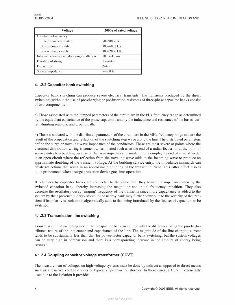
4.1.2.2 Capacitor bank switching
Capacitor bank switching can produce severe electrical transients. The transients produced by the directswitching (without the use of pre-charging or pre-insertion resistors) of three-phase capacitor banks consistof two components:
a) Those associated with the lumped parameters of the circuit are in the kHz frequency range as determinedby the equivalent capacitance of the phase capacitors and by the inductance and resistance of the buses, cur-rent-limiting reactors, and ground path.
b) Those associated with the distributed parameters of the circuit are in the MHz frequency range and are theresult of the propagation and reflection of the switching step wave along the line. The distributed parametersdefine the surge or traveling wave impedance of the conductors. These are most severe at points where theelectrical distribution wiring is somehow terminated such as at the end of a radial feeder, or at the point ofservice entry to a building because of the large impedance mismatch. For example, the end of a radial feederis an open circuit where the reflection from the traveling wave adds to the incoming wave to produce anapproximate doubling of the transient voltage. At the building service entry, the impedance mismatch cancreate reflections that result in an approximate doubling of the transient current. This latter effect also isquite pronounced when a surge protection device goes into operation.
If other nearby capacitor banks are connected to the same line, they lower the impedance seen by theswitched capacitor bank, thereby increasing the magnitude and initial frequency transition. They alsodecrease the oscillatory decay (ringing) frequency of the transients since more capacitance is added to thesystem by their presence. Energy stored in the nearby bank may further contribute to the severity of the tran-sient if its polarity is such that it algebraically adds to that being introduced by the first set of capacitors to beswitched.
4.1.2.3 Transmission line switching
Transmission line switching is similar to capacitor bank switching with the difference being the purely dis-tributed nature of the inductance and capacitance of the line. The magnitude of the line-charging currenttends to be substantially less than that for power-factor capacitor bank switching, but the system voltagescan be very high in comparison and there is a corresponding increase in the amount of energy beingrerouted.
4.1.2.4 Coupling capacitor voltage transformer (CCVT)
The measurement of voltages on high-voltage systems must be done by indirect as opposed to direct meanssuch as a resistive voltage divider or typical step-down transformer. In these cases, a CCVT is generallyused due to the isolation it provides.
Voltage 200% of rated voltage
Oscillation Frequency
Line disconnect switch 50–300 kHz
Bus disconnect switch 300–600 kHz
Low-voltage switch 300–2000 kHz
Interval between each decaying oscillation 10 µs–16 ms
Duration of string 1 ms–4 s
Decay time 2–4 s
Source impedance 5–200 Ω
8 Copyright © 2005 IEEE. All rights reserved.
标准分享网 www.bzfxw.com 免费下载
IEEE
CONTROL EQUIPMENT GROUNDING IN GENERATING STATIONS Std 1050-2004
The capacitors in these devices along with the inductance of the power system conductors constitute a reso-nant circuit whose frequency can be in the MHz range. Any oscillatory high-frequency transients occurringon the high-voltage bus can give rise to high-frequency currents that are coupled through the capacitors tothe signal and control circuits.
The transformer located in the base of the CCVT contains a distributed stray capacitance of a few hundredpF between the secondary winding and the core and the Faraday shield. This capacitance is the circuit ele-ment closing a loop, which in turn links the transient magnetic flux between the power ground conductorand the nearby signal cable. Transient potentials of up to 10 kV have been measured in signal cables.
Almost identical problems are present in current transformers that have wound capacitance bushings.
4.1.2.5 Gas insulated switchgear (GIS)
Typical GIS equipment often has faster contact operating time than air-insulated equipment and the gasallows the contact’s arcs to be more quickly extinguished. This combination of effects produces fasterswitching transition times, which result in higher frequency disturbances being created than are produced inair-insulated equipment.
During the operation of GIS, the high-voltage gradients caused by restrikes between contacts, induce travel-ing waves that are confined to the inside of the GIS enclosure by skin effect. They travel along the GIS andare divided and reflected at junctions, but are confined by any open circuit breakers or disconnect switchesalong the path of propagation. Only when discontinuities or breaks in the enclosure are encountered dopotentials transfer to the exterior enclosure surface and result in noise voltages. The most common enclosurediscontinuities are SF6-to-air terminations, cable potheads (with insulated flanges) and, for some switchgear,current transformers. The SF6-to-air termination represents by far the largest enclosure discontinuity andhence the largest source of noise voltages in most GIS. This location represents a critical coupling area forcontrol and signal cables.
Typical values for GIS measured at the bushing:
Voltage: 40%-70% of rated voltage
Oscillation Frequency: 5–50 MHz
Duration at Flashover: 40 ns
Duration at Disconnect Operation: 170 ms string of pulses
The GIS ground connections are typically lengthy due to the installation height above ground that equipmentof this type is often associated with. Therefore, as a result of L(di/dt) effects, they are almost always tooinductive to effectively reduce these high-frequency noise voltages. Also, they usually act as efficient radia-tors or EMI from the corresponding antenna effects when their length is >1/20th of a wavelength at theEMI’s fundamental frequency. Two of the best solutions for minimizing electrical noise are to physicallydistance the sensitive victim instrument and control systems from these areas, and to fully shield the victimequipment and filter all conductors that penetrate the victim equipment’s metal enclosures.
4.1.2.6 Vacuum insulated switchgear (VIS)
This equipment is similar to GIS except that the environment for the contacts is a vacuum as opposed to agas. Therefore, as a result of faster arc extinguishing time during contact bounce or opening, this type ofequipment is capable of producing even faster transient voltage and current wavefronts from its operationthan equivalent GIS equipment.
Copyright © 2005 IEEE. All rights reserved. 9
IEEEStd1050-2004 IEEE GUIDE FOR INSTRUMENTATION AND
4.1.2.7 Earth ground voltage differences
Earth grounding systems that extend over large areas have sufficient point-to-point earth impedance to cre-ate a difference in voltage between two points within the system during transient fault events and lightningstrike conditions. The conduction of these types of power-system transients through the grounding system isone of the most common causes of large ground potential differences from the related impedance effects. Atypical transient represents an ac signal of 1 kHz or greater and the path for the transient current will be par-allel to the path of the associated power system conductors.
Earth ground offset voltages may only be minimized by making better connections to the earth when theoverall distance between the two points of interest can be viewed under the conditions of circuit analysis.This is generally when the distance is less than 1/20 λ at the frequency of interest. When the distance thecurrent has to travel between points in the earth exceeds 1/20 λ, then transmission and wave theory must beused and there is no practical means to keep all points at or even very near the same potential. Hence, atsome critical frequency the earth grounding system cannot be used in any sense as a means of equalizingpotentials or minimizing unwanted current flows between points on its surface when they exceed 1/20 λ, nomatter how good a connection to earth has been made.
4.1.2.8 Current transformers (CTs)
Saturation of current transformer cores by excessive primary current (dc or ac) can induce very high volt-ages in the secondary windings and thence onto the conductors attached to them. This phenomenon isrepeated for each transition from saturation in one direction to saturation in the other, so it may occur on acycle-to-cycle basis. AC problems occur simply because of too much primary current for the CT design,while dc problems are typically associated with the effects of lightning. The unwanted transient voltageappearing in the secondary circuit consists of high-magnitude spikes having alternating polarity and persist-ing for a few milliseconds every half-cycle for the duration of the overcurrent condition.
4.1.2.9 Electro-mechanical equipment
Electro-mechanical equipment and some forms of rotating equipment, such as that containing unshieldedwindings or fields, centrifugal switches, armature brushes, or slip-rings, contain many possible internalsources of high-frequency interference. These include:
a) Partial (corona) discharges within the stator winding insulation of motors. Note that this can alsooccur on dry-type transformers.
b) Slot discharges between coil surfaces and the stator iron.
c) Sparking from exciters with brushes.
d) Arcing associated with conductor strands that have fractured from copper fatigue. This arcing is notcontinuous but is caused by a movement of conductor surfaces as a result of steady-state and tran-sient magnetic forces.
e) DC machine brushes.
f) Centrifugal switch contact operation and arcing.
g) Older types of non metal-enclosed or other inadequately shielded motor-controllers with arcing con-tacts. These may be of the manual or contactor type. Non-interlocked, manually operated reversingand motor “plugging” types of controls are potential problem sources since they may be operatedwhile the motor is still spinning.
h) Variable frequency or pulse inverter drives. These are also capable of producing both conductiveand radiated EMI from the fast transition times associated with SCR, IGBT, or similar motorinverter-driver switching schemes. The largest number of conducted EMI problems involving thistype of equipment occur in the range of the first 100 harmonics of the fundamental frequency of thedriver circuit.
10 Copyright © 2005 IEEE. All rights reserved.
标准分享网 www.bzfxw.com 免费下载
IEEE
CONTROL EQUIPMENT GROUNDING IN GENERATING STATIONS Std 1050-2004
i) Distributed capacitance. A motor that is being initially energized or in some cases de-energized iscapable of coupling a transient current from its winding to its metal frame/enclosure and thence intothe associated equipment grounding system for that motor. The coupling mechanism, in this case, isthe distributed capacitance from the winding to the case and is proportional to motor size andvoltage rating. Large motors operating at medium voltage can produce the greatest EMI effects, par-ticularly since these typically have a large number of associated I&C circuits.
4.1.2.10 Silicon controlled rectifiers (SCRs)
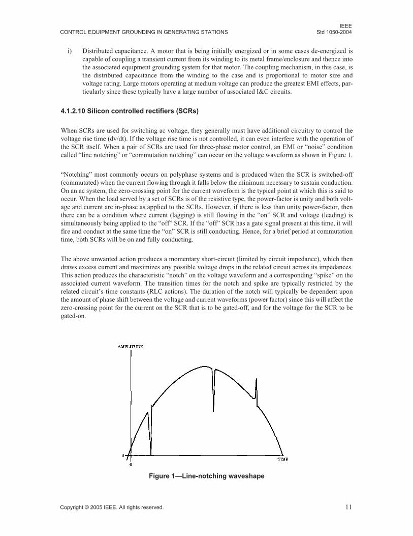
When SCRs are used for switching ac voltage, they generally must have additional circuitry to control thevoltage rise time (dv/dt). If the voltage rise time is not controlled, it can even interfere with the operation ofthe SCR itself. When a pair of SCRs are used for three-phase motor control, an EMI or “noise” conditioncalled “line notching” or “commutation notching” can occur on the voltage waveform as shown in Figure 1.
“Notching” most commonly occurs on polyphase systems and is produced when the SCR is switched-off(commutated) when the current flowing through it falls below the minimum necessary to sustain conduction.On an ac system, the zero-crossing point for the current waveform is the typical point at which this is said tooccur. When the load served by a set of SCRs is of the resistive type, the power-factor is unity and both volt-age and current are in-phase as applied to the SCRs. However, if there is less than unity power-factor, thenthere can be a condition where current (lagging) is still flowing in the “on” SCR and voltage (leading) issimultaneously being applied to the “off” SCR. If the “off” SCR has a gate signal present at this time, it willfire and conduct at the same time the “on” SCR is still conducting. Hence, for a brief period at commutationtime, both SCRs will be on and fully conducting.
The above unwanted action produces a momentary short-circuit (limited by circuit impedance), which thendraws excess current and maximizes any possible voltage drops in the related circuit across its impedances.This action produces the characteristic “notch” on the voltage waveform and a corresponding “spike” on theassociated current waveform. The transition times for the notch and spike are typically restricted by therelated circuit’s time constants (RLC actions). The duration of the notch will typically be dependent uponthe amount of phase shift between the voltage and current waveforms (power factor) since this will affect thezero-crossing point for the current on the SCR that is to be gated-off, and for the voltage for the SCR to begated-on.
Figure 1—Line-notching waveshape
Copyright © 2005 IEEE. All rights reserved. 11
IEEEStd1050-2004 IEEE GUIDE FOR INSTRUMENTATION AND
4.1.2.11 Digital Logic-Based systems (computers, controllers, and related equipment)
The harmonic noise generated by microprocessor and memory boards within an item of equipment such as acomputer, is dependent primarily upon its system clock frequency. The highest noise frequency, however,will be a harmonically related function of the rise and fall times of the clock pulse, whichever is faster. Forexample, a digital signal with a rise time of 3 ns is roughly equivalent to a 100 MHz sine wave.
While the above noise is usually well confined within the properly shielded and filtered equipment’s cabi-net, which has been compliance tested per the emissions standards of the country of origin, it can escape intothe environment by conducted, radiated, or both means if that enclosure is modified or left opened, its poweror signal cable port filtering is defeated, or it is penetrated by a foreign, unfiltered conductor of some typesuch as a field installed signal, power, or grounding conductor. For similar reasons, the various computersubsystems and peripheral devices can contribute significantly to the noise generated by the total computersystem, especially via EMI “leakage” from the interconnecting, power, signal, and control connectors andcables. This is especially the case when connectors and cables are field fabricated and have not been for-mally test certified to be compatible with the original equipment. This is generally not a problem with acpower cables that make connections to factory-provided, field-wiring compartments or associated recepta-cle/plug style connections that are integral to the compliant equipment.
The major contributing devices to EMI have the following characteristics:
a) CRT display. Noise sources within a CRT display are the video circuitry (typical 20–50 V swing at10–20 MHz) and the horizontal yoke drive circuitry (typical 3 A peak-to-peak amplitude at 10–20MHz). Near-field EMI in the form of very low-frequency H-fields up to several tens of kHz from thehorizontal yoke itself, are also encountered. This latter condition is a common problem when two ormore CRT displays are placed very close to one another and the mutual EMI coupled between themaffects the stability of the raster and produces effects such as slowly wavy lines, swimming display,or horizontal bands rolling up or down.
b) Switching power supply. The radiated noise generated by these devices is dependent upon theswitching frequency (typical 10–100 kHz) and the switching amplitude. These devices also providelarge amounts of EMI in the form of conducted harmonic current waveform distortion on the acpower supply wiring up to a few kHz. Most of this conducted EMI will involve odd-ordered har-monics from the ac system’s fundamental.
c) Printers. The major noise sources for these devices fall into two categories. For impact printers, theEMI is generated from the drivers and collapsing fields of printhead solenoids and the printhead orcarriage positioning motors along with the associated internal wiring to and from them. For laserprinters, the EMI is generated by the gated SCR or transistor switched power control circuits that areused to control the current for high-intensity drum erasure lamps and the heaters used with tonerfuser rolls.
d) Cabling. One of the most overlooked sources of radiated EMI noise in a computer system is theinterconnect cabling. The noise generated is dependent upon the signal level, the number of conduc-tors within each cable and their physical orientation (symmetry of twisting or lack thereof), and thetype of shielding provided if any. The connectors used at the ends of these cables are also known tobe a point of EMI emission if they are not properly shielded and grounded. Crosstalk between differ-ent circuits being carried in the same cable is also a common means of EMI propagation on thesecables.
4.1.2.12 DC control circuits
One of the major causes of transient overvoltages within a dc control circuit is the energizing of an induc-tance within a circuit. This induced voltage may be defined as:
12 Copyright © 2005 IEEE. All rights reserved.
标准分享网 www.bzfxw.com 免费下载
IEEE
CONTROL EQUIPMENT GROUNDING IN GENERATING STATIONS Std 1050-2004
(1)
where I is the current through the coil, L is the inductance of the coil, C is the stray capacitance of the circuit.
The involved inductance may consist of both discrete and distributed circuit elements. The involvedcapacitance may consist of the distributed wiring or stray capacitance plus any lumped capacitance fromconnected components. The current of interest is the value of the current at the instant the circuit is deener-gized by switching open the power source at any point in the circuit.
EMI impulses in excess of 3 kV can be produced by interrupting the current in highly inductive devices suchas a solenoid or a thermal-magnetic circuit breaker’s magnetic trip coil. Arcing across the electromechanicalcontacts will tend to limit the magnitude of the impulses (an increasing air-gap and arc represents increasingimpedance). As a general rule and with the exception of lightning-induced impulses, electrostatically ormagnetically induced ac voltages or currents from nearby external circuitry and conductors are relativelysmall in magnitude when compared to the internal inductive impulses induced in dc control circuits on theirown wiring.
4.1.2.13 Mechanical vibration
Mechanical vibration and shock can produce arc discharge EMI whenever loose electrical connections aremoved or electromechanical switch contacts bounce open or closed and produce an arc discharge. This istrue even for low-voltage circuits, since voltages as low as 9 V across gold alloy contacts can produce an arcdischarge. Also, many low-voltage circuits can involve the switching of very large amounts of available cur-rent. Power supply buses rated at ±5, ±12 Vdc logic and 12, 24, or 48 Vdc control power are commonlyrated for several tens of continuous amperes to more than a hundred amperes on larger items of equipment.
Terminal blocks, electrical components with loose connections, or poorly made splices in conductor pathsare common points on a wiring system where vibration causes problems to occur. When metallic conduit orother raceway fittings necessary for EMI shielding and equipment ground integrity vibrate loose, they canproduce an ineffective shielding connection, an arc discharge that will rapidly change the otherwise stablecurrent flow in the affected path, radiation of high-frequency noise, or combinations of these three problems.
4.1.2.14 Chemical contamination
Most industrial facility atmospheres contain suspended chemicals (such as oil, coolants, or degreasing solu-tions) that may settle on electrical equipment.
Even though liquid and even gas-tight electrical connections should normally be immune to this method ofcontamination, vibration and temperature changes may compromise the normally sealed electrical connec-tion. For example, vibration causes normally sealed connections to flex or linearly move in and out of theseal and thereby permit the entrance of chemical contaminants that are riding on the surface of the conductorduring its motions. In addition, many electrical connections and their seals are made with mechanically dis-similar materials that have different coefficients of expansion and contraction. Therefore, temperaturechanges will also cause the conductors passing through the seals in these kinds of connections to both expe-rience changes in the radial clearances and sealing pressure of the seal as well as changes in length, theeffects of which can combine and permit contaminants to enter.
Human hands can also introduce chemical contamination during the assembly of system components. Con-nections should be well cleaned of all contamination before mechanical bonding or sealing takes place.
V I LC----=
Copyright © 2005 IEEE. All rights reserved. 13
IEEEStd1050-2004 IEEE GUIDE FOR INSTRUMENTATION AND
Any time water or a chemical contaminant can get in between two metal items and especially when they areof dissimilar materials from widely spaced regions on the galvanic series, a semi-conducting joint is createdthat may also act as a wet-cell battery with a small potential across the joint. Such an unwanted type of jointis created when the contaminant acts as the electrolyte and the two metals assume the role of anode and cath-ode depending upon where they stand on the galvanic series. By itself, this electrochemical activity becomesa problem is two ways. The first is that the metal may literally be eaten away due to the corrosive action ofelectrolysis, and the second is that the developed potential may be considered a point-source of EMI.
A third form of EMI problem also exists that may be more of a problem in some cases. In this case, the elec-trochemical action of the contaminated joint is not usually of concern in the direct creation of the EMI.Instead, it generally takes an externally induced or conducted current to be forced through it in order for theproblem to fully emerge. This kind of EMI problem is typically a radiated type (but it can also be conductiveon the involved path) and it occurs since the electrochemical joint is a rectifying, semiconducting path. Assuch, it represents a non-linear impedance to any current flow forced through it. This non-linear impedancecreates harmonic current and related voltage waveform distortion of the current’s fundamental frequency asit conducts. Thus, a fundamental frequency current passing through such a non-linear conducting joint willsuddenly be combined with a number of higher-order, harmonically-related currents, each of which will beboth conducted and radiated to whatever degree is possible on the circuit. This is especially a problem whenthere is a strong source of radio-frequency energy nearby where such a joint can begin unintentionally actingas a part of an antenna circuit. Examples of external sources of exciting current are those created from anintentional radiator such as a transmitter, or from an unintentional one such as nearby arcing contacts, orcorona discharge on HV equipment. A natural source of exciting current is nearby lightning.
4.1.2.15 Human interaction via electrostatic discharge (ESD)
The electrostatic discharge (ESD) occurs when an electrostatically charged operator touches and therebydischarges via some part of the victim equipment. For example, external ESD may occur to metallicallyenclosed equipment, its data or signal cables and connectors, or its exposed controls. This is a known andserious type of EMI problem. Also, a lack of good ESD practices by personnel may cause ESD to occurwithin victim equipment and directly onto sensitive circuits and components due to careless handling of cir-cuit plug-in cards, connectors, and similar internal components.
While ESD is typically associated with conditions of low relative humidity, the involvement of ESD pronematerials (those that are widely spaced on the triboelectric table) as used for clothing articles, shoes, andwalking or working surfaces can clearly exacerbate an otherwise harmless problem. Thus, an ESD problemcan be experienced over a much wider range of relative humidity conditions than might be expected by alack of attention to the needed use of ESD resistant materials.
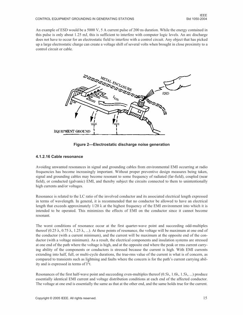
An example of ESD ingress to a victim circuit is shown in Figure 2 where a metallic switch body is mountedon a printed circuit board, but is isolated from the conductive cabinet. The ESD current will create both con-ducted and radiated noise in the victim equipment as it conductively flows to ground via the printed circuitboard’s traces and wiring capacitances. Once the ESD current enters the equipment’s wiring harness or logicpower supply distribution bus system, it is also free to radiate in far-field fashion within the equipment andto near-field couple to adjacent conductors and components. This allows the ESD to produce singular orsimultaneous multiple failure symptoms in the equipment, and often over widely spaced areas. Hence, anESD at one point in the victim equipment may produce its unwanted effects some distance away within theequipment on other circuits.
An ESD that occurs directly to a poorly grounded/bonded metal cabinet’s door or side-panel is also a knownEMI problem in that the large sheet metal area acts as a plane-wave radiator; therefore, when the ESDstrikes the external surface, its wavefront also travels through the thickness of the door or panel and is re-radiated from the inside surface into the enclosure’s volume containing the ESD susceptible circuits.
14 Copyright © 2005 IEEE. All rights reserved.
标准分享网 www.bzfxw.com 免费下载
IEEECONTROL EQUIPMENT GROUNDING IN GENERATING STATIONS Std 1050-2004
An example of ESD would be a 5000 V, 5 A current pulse of 200 ns duration. While the energy contained inthis pulse is only about 1.25 mJ, this is sufficient to interfere with computer logic levels. An arc dischargedoes not have to occur for an electrostatic field to interfere with a control circuit. Any object that has pickedup a large electrostatic charge can create a voltage shift of several volts when brought in close proximity to acontrol circuit or cable.
4.1.2.16 Cable resonance
Avoiding unwanted resonances in signal and grounding cables from environmental EMI occurring at radiofrequencies has become increasingly important. Without proper preventive design measures being taken,signal and grounding cables may become resonant to some frequency of radiated (far-field), coupled (nearfield), or conducted (galvanic) EMI, and thereby subject the circuits connected to them to unintentionallyhigh currents and/or voltages.
Resonance is related to the LC ratio of the involved conductor and its associated electrical length expressedin terms of wavelength. In general, it is recommended that no conductor be allowed to have an electricallength that exceeds approximately 1/20 λ at the highest frequency of the EMI environment into which it isintended to be operated. This minimizes the effects of EMI on the conductor since it cannot becomeresonant.
The worst conditions of resonance occur at the first quarter-wave point and succeeding odd-multiplesthereof (0.25 λ, 0.75 λ, 1.25 λ, ...). At these points of resonance, the voltage will be maximum at one end ofthe conductor (with a current minimum), and the current will be maximum at the opposite end of the con-ductor (with a voltage minimum). As a result, the electrical components and insulation systems are stressedat one end of the path where the voltage is high, and at the opposite end where the peak or rms current carry-ing ability of the components or conductors is stressed because the current is high. With EMI currentsextending into half, full, or multi-cycle durations, the true-rms value of the current is what is of concern, ascompared to transients such as lightning and faults where the concern is for the path’s current carrying abil-ity and is expressed in terms of I2t.
Resonances of the first half-wave point and succeeding even-multiples thereof (0.5λ, 1.0λ, 1.5λ, ...) produceessentially identical EMI current and voltage distribution conditions at each end of the affected conductor.The voltage at one end is essentially the same as that at the other end, and the same holds true for the current.
Figure 2—Electrostatic discharge noise generation
Copyright © 2005 IEEE. All rights reserved. 15
IEEEStd1050-2004 IEEE GUIDE FOR INSTRUMENTATION AND
Conductors installed in free-space will have self-resonant points that will normally be somewhat higher infrequency than those installed in close proximity to the earth, or in particular ferrous metal items. This is theresult of mutual coupling that exists between the conductor and the earth or ferrous items, and the result isgenerally that the self-resonant frequency of the conductor is lowered. In addition, depending upon theamount of stray coupling involved, the velocity factor of the path is also generally reduced to values that areless then that of a conductor in free space.
The full-wave, self-resonant frequency of a conductor in free space may be estimated by Equation (2):
f = c/l (2)
Where c is the speed of propagation in free space, approximately 300 meters per microsecond. Measuringtime in microseconds yields a result for f in megahertz.
Equation (2) may be used to approximate the self-resonant conditions of a cable or grounding conductor’spath. If the result is divided by 20, the 1/20 λ point may be estimated and used as a recommended limit. Sim-ilarly, dividing the result by 4.0 or by 2.0 respectively gives the quarter-wave point and half-wave pointestimates. Rearranging the equation allows the estimated length of the conductor to be determined in view ofa given amount of EMI frequency.
4.1.2.17 Reflections and traveling waves
Excessively high currents and voltages on EMI affected cables, or grounding conductors may also occurfrom traveling waves on the path, which encounter a severe impedance mismatch such as an open orshorted-end. In this type of situation, the traveling wave is partially or fully reflected by the impedance mis-match and the reflected portion is instantaneously added to the original wave at the point of reflection. As aresult, the current or voltage at such a point may easily be doubled.
In the case of an open-end termination such as at the end of an overhead radial distribution feeder, theimpedance is very high (open circuit), so the reflection occurs on the voltage waveform and not the currentwaveform. There is no current flow in the open circuit, but a very high potential may be created. In the caseof a short-circuit termination such as where a surge-arrester is applied on the end of an overhead radial dis-tribution feeder, the impedance is very low (it approaches a short-circuit condition in respect to the travelingwave), so the reflection occurs on the current waveform and not on the voltage waveform. There is littlevoltage developed across a “short circuit.”
EMI conditions at or near the shorted or open-end termination for a traveling wave can be very severe. Forexample, near-field conditions are worst for H-fields nearest the shorted-termination (highest current, lowestvoltage) while E-field conditions are similarly serious nearest the open-termination (highest voltage, lowestcurrent). Radiation of far-field EMI can occur all along the conductor’s path once it is subjected to EMI,which forms a traveling wave on it. Hence, unwanted EMI effects are unavoidable under these kinds of con-ditions if there are any victim power, signal, grounding, or other conductors located near the conductor car-rying the traveling wave.
4.1.2.17.1 Velocity factor
Traveling waves move through a conductive medium (such as a wire) at a velocity that may be considerablyless than that for the radiated wave in free space or air. The free space velocity factor of 1.0x is approxi-mately 299 m/s for a radiated wave. Velocity factors less than 1.0x always occur when a wave travelsthrough a physical medium such as a wire, and this affects calculations regarding how long a conductor maybe in relation to conditions of actual self-resonance vs. equivalent free space electrical length.
For example, the leading edge (first transition) of a radiated wave will travel 30 m in free space during onecycle of a 10 MHz clock signal in a microprocessor. However, within an insulated conductor in a cable, it
16 Copyright © 2005 IEEE. All rights reserved.
标准分享网 www.bzfxw.com 免费下载
IEEECONTROL EQUIPMENT GROUNDING IN GENERATING STATIONS Std 1050-2004
may travel only 21 m due to a reduced velocity factor, which, in this case, would be 0.7x (21m/30m = 0.7).If the voltage wave reflects from the cable termination where the cable has been terminated “open” or atleast in a very high impedance in comparison to the signal cable’s characteristic impedance, and is in phasewith a new wave, resonance will occur and line oscillations will be greatly magnified. Also, if one end of thecircuit is grounded, the first resonance at 10 MHz occurs when the conductor is only 5.25 m or 1/4 wave-length long.
At this frequency, the 5.25 m long cable appears to be virtually an open circuit between ends or at least avery high impedance. It is incapable of equalizing the voltages appearing between its ends. A cable orgrounding conductor, longer than 1/20 λ cannot be counted upon to adequately equalize voltages between itsends. This amounts to only 1.5 m of length at 10 MHz, so it should become apparent that the use of longgrounding/bonding conductors in a facility that is a part of a “single-point” or similar grounding system willnot be effective for high-frequency EMI.
At high frequencies, signal transmission lines are often terminated in their characteristic surge impedance toeliminate most of the reflection and resonance. However, no single-grounded conductor within a cable canprovide a virtual short circuit between one end and the other over a very useful portion of a broad frequencyrange, and not at all once 1/4 λ conditions and odd-multiples thereof, are approached.
4.1.2.18 Power circuit inrush current
Small conductors on higher impedance circuits carrying small amounts of current cannot induce significanttransient voltages and currents into larger power conductors on low-impedance circuits. This is the result ofthe relative impedance of the respective circuits and limits on how fast a large current change can beimpressed onto the path. However, the reverse situation is of major concern. Where I&C circuits are placednearby to power conductors, the likelihood of transient voltages and currents being coupled to the instru-mentation and control circuits is very high.
The transients produced by the unwanted near-field coupling can electromagnetically induce voltages thatcreate current transients in the I&C circuits installed near these power cables. This can occur when thepower circuit is energized and acts as a primary winding for an air-core transformer with the nearby I&C cir-cuit act as the secondary winding.
4.1.2.19 Other incidental sources
Noise can also be generated by such sources such as transformer and motor inrush currents, load tap-chang-ing, flashover of gaps from overvoltages, ferroresonance, impulse testing, megger testing, low-voltagebreaker and contactors, and corona discharge from high-voltage transmission lines. Noise from transmissionline corona can occur miles from the point of generation by propagating along the line.
Local incidental sources of EMI may also occur as a result of electrostatic filters in HVAC systems, ozonegenerators used with water purification systems, neon signs, and “bug-zappers.” Unfiltered SCR circuitsused to phase-control incandescent lighting systems also generate EMI in both radiated and conducted form.High- and low-pressure sodium lighting fixtures contain arcs and can produce EMI if they are not shielded.This also applies to mercury vapor lighting fixtures. Both forms of lighting fixtures may radiate high-frequency EMI unless shielded, and both will conduct low-frequency EMI back onto the ac power system inthe form of harmonic current and voltage waveform distortion unless harmonic filtering is provided at thefixture to prevent this.
Electric arc welders also create EMI at the arc, and both conduct it onto the connected ac power system andradiate it into the environment by the loop-antenna (far field) and transformer primary effects (near-field)that the welding cables can create if they are used without tightly twisting them together. Voltages used inthe arc-welding process are fairly low, while peak and rms currents may be quite high. Hence, E-field EMIis not as much a problem as is H-field EMI.
Copyright © 2005 IEEE. All rights reserved. 17
IEEEStd1050-2004 IEEE GUIDE FOR INSTRUMENTATION AND
4.1.3 Intentional sources
Many devices intentionally use radio frequency (RF) energy to accomplish their function, such as hand-heldtransceivers (cellular telephones, broadcast transmitters, security guard transceivers, citizen’s band radios),RF-stabilized arc welders, induction heaters and RF electrostatic drying equipment. These devices produceconsiderable amounts of RF energy, which generally is not contained and can therefore reach I&C equip-ment.
Proximity effects can easily offset the fact that a radiating source of EMI is otherwise “low-power.” Forexample, an 800 MHz cellular phone does not radiate much peak power by itself, but if brought into closeproximity to victim circuits such as those within an electronic equipment cabinet with the door open, consid-erable EMI can be coupled into these circuits. Unlike most two-way radio equipment, cellular telephonesradiate even when they are not in actual two-way use by their operator since they must periodically notifythe cellular site’s computer that they are on and where they are so that incoming calls may be received.
4.2 Noise-coupling methods
Noise can be coupled into (or transmitted from) control circuits by any one of four different methods:
a) Conductive (common impedance, galvanic, arcing, or direct contact)
b) Capacitive (electric)
c) Inductive (magnetic)
d) Radiation (electromagnetic)
Both capacitive and inductive coupling refer primarily to near-field coupling. This is also often referred to asthe reactive field where the energy is stored or as stray (parasitic) reactive coupling. A control circuit orcable is considered to be in the near field of an electromagnetic source when the source to circuit distance isless than l/6 λ of the highest source frequency. Radiation coupling refers to circuits located in the far field ofa source where the source’s emissions are seen as a true traveling electromagnetic wave. This latter situationinvolves radio wave transmissions and antennae effects.
Each of these coupling methods will be detailed in a following subclause.
4.2.1 Characteristics of electromagnetic fields
Electromagnetic waves consist of two oscillating fields at right angles to one another: the electric field (E-field) and the magnetic field (H-field). The electromagnetic wave impedance (Zw) in ohms is defined as theratio of the E-field intensity expressed in V/m to the H-field intensity expressed in A/m. In the reactive ornear field, where the energy is stored, the E-field and H-field can be considered independently where thewave impedance does not apply.
E-fields are generated by and most easily interact with high-impedance, voltage-driven circuitry, such as astraight wire or dipole. E-fields are most readily coupled by capacitor action. H-fields are generated by andmost readily interact with low-impedance, current-driven circuitry, such as a wire loop. H-fields are mostreadily coupled by transformer action.
Both the electric and magnetic fields are perpendicular to the direction of propagation of the electromagneticwave. The value of Zw for a plane wave propagating through air (free space) is 377 Ω.
4.2.2 Common impedance coupling
Conductive coupling is also known as common impedance coupling, and can be created by galvanic actionor an arc. As shown in Figure 3, when two or more circuits share a wire or conductor as a common section of
18 Copyright © 2005 IEEE. All rights reserved.
标准分享网 www.bzfxw.com 免费下载
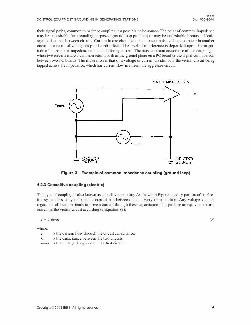
IEEECONTROL EQUIPMENT GROUNDING IN GENERATING STATIONS Std 1050-2004
their signal paths, common impedance coupling is a possible noise source. The point of common impedancemay be undesirable for grounding purposes (ground loop problem) or may be undesirable because of leak-age conductance between circuits. Current in one circuit can then cause a noise voltage to appear in anothercircuit as a result of voltage drop or Ldi/dt effects. The level of interference is dependent upon the magni-tude of the common impedance and the interfering current. The most common occurrence of this coupling iswhen two circuits share a common return, such as the ground plane on a PC board or the signal common busbetween two PC boards. The illustration is that of a voltage or current divider with the victim circuit beingtapped across the impedance, which has current flow in it from the aggressor circuit.
4.2.3 Capacitive coupling (electric)
This type of coupling is also known as capacitive coupling. As shown in Figure 4, every portion of an elec-tric system has stray or parasitic capacitance between it and every other portion. Any voltage change,regardless of location, tends to drive a current through these capacitances and produce an equivalent noisecurrent in the victim circuit according to Equation (3):
I = C de/dt (3)
where: I is the current flow through the circuit capacitance,C is the capacitance between the two circuits,de/dt is the voltage change rate in the first circuit.
Figure 3—Example of common impedance coupling (ground loop)
Copyright © 2005 IEEE. All rights reserved. 19
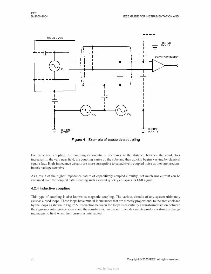
IEEEStd1050-2004 IEEE GUIDE FOR INSTRUMENTATION AND
For capacitive coupling, the coupling exponentially decreases as the distance between the conductorsincreases. In the very near field, the coupling varies by the cube and then quickly begins varying by classicalsquare-law. High-impedance circuits are more susceptible to capacitively coupled noise as they are predom-inately voltage sensitive.
As a result of the higher impedance nature of capacitively coupled circuitry, not much rms current can besustained over the coupled path. Loading such a circuit quickly collapses its EMI signal.
4.2.4 Inductive coupling
This type of coupling is also known as magnetic coupling. The various circuits of any system ultimatelyexist as closed loops. These loops have mutual inductances that are directly proportional to the area enclosedby the loops as shown in Figure 5. Interaction between the loops is essentially a transformer action betweenthe aggressor interference source and the sensitive victim circuit. Even dc circuits produce a strongly chang-ing magnetic field when their current is interrupted.
20 Copyright © 2005 IEEE. All rights reserved.
标准分享网 www.bzfxw.com 免费下载
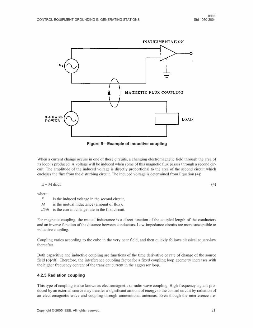
IEEECONTROL EQUIPMENT GROUNDING IN GENERATING STATIONS Std 1050-2004
When a current change occurs in one of these circuits, a changing electromagnetic field through the area ofits loop is produced. A voltage will be induced when some of this magnetic flux passes through a second cir-cuit. The amplitude of the induced voltage is directly proportional to the area of the second circuit whichencloses the flux from the disturbing circuit. The induced voltage is determined from Equation (4):
E = M di/dt (4)
where: E is the induced voltage in the second circuit,M is the mutual inductance (amount of flux),di/dt is the current change rate in the first circuit.
For magnetic coupling, the mutual inductance is a direct function of the coupled length of the conductorsand an inverse function of the distance between conductors. Low-impedance circuits are more susceptible toinductive coupling.
Coupling varies according to the cube in the very near field, and then quickly follows classical square-lawthereafter.
Both capacitive and inductive coupling are functions of the time derivative or rate of change of the sourcefield (dφ/dt). Therefore, the interference coupling factor for a fixed coupling loop geometry increases withthe higher frequency content of the transient current in the aggressor loop.
4.2.5 Radiation coupling
This type of coupling is also known as electromagnetic or radio wave coupling. High-frequency signals pro-duced by an external source may transfer a significant amount of energy to the control circuit by radiation ofan electromagnetic wave and coupling through unintentional antennas. Even though the interference fre-
Figure 5—Example of inductive coupling
Copyright © 2005 IEEE. All rights reserved. 21
IEEEStd1050-2004 IEEE GUIDE FOR INSTRUMENTATION AND
quencies may be much higher than those to which the control circuit will normally respond, they canbecome troublesome if they are modulated at the source by switching or by the ac power frequency or itsharmonics and then picked up and non-linearly demodulated or rectified by the control circuit. This processof pickup and demodulation can produce additional harmonically related spurious signals in the victiminstrument or control circuit. This circuit may then become a local re-radiation source of the EMI at the fun-damental or harmonically-related frequency from antenna effects of the victim circuit’s wiring.
4.2.6 Interference modes
4.2.6.1 Common-mode interference
This type of interference is also known as longitudinal-mode interference. It is simultaneously introducedinto all of the conductors of the signal path, including its grounding conductor if it has one. As a result of thesimultaneous nature of the introduction of the CM interference, little, if any, potential difference may beseen between the victim conductors. Instead, significant potential differences are generally seen to existbetween all of the victim conductors and the circuits and ground reference for the circuit the victim conduc-tors are terminated. This is illustrated by Figure 6.
CM currents are most commonly caused by equal electrical pickup in a pair of conductors, and in paths ofequal impedance will be essentially equal. If the CM current’s affected paths are of differing impedance,then the CM current will be inversely proportional to the impedance presented by each victim conductorpath forming the loop.
CM interference acts indirectly on the victim receiver. Therefore, a signal error must be preceded by a con-version from common-mode interference to differential-mode (DM) interference. A purely CM surgebetween separate grounds as shown in Figure 6 will be almost completely rejected by a well-balanced, dif-ferential amplifier. Connecting one side of the differential amplifier to ground will produce a differential-mode surge. Transformer coupling without using carefully balanced, center-tapped windings referenced tosignal ground will produce DM interference by the CM to DM conversion that takes place as a result of thewinding’s geometry.
Mismatched impedances of passive components (resistors, capacitors, and inductors) used in the transmis-sion of balanced signals through circuits also contribute to the conversion of CM to DM current or voltage inthe victim circuit.
22 Copyright © 2005 IEEE. All rights reserved.
标准分享网 www.bzfxw.com 免费下载
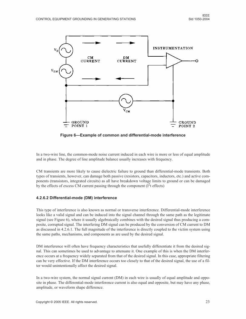
IEEECONTROL EQUIPMENT GROUNDING IN GENERATING STATIONS Std 1050-2004
In a two-wire line, the common-mode noise current induced in each wire is more or less of equal amplitudeand in phase. The degree of line amplitude balance usually increases with frequency.
CM transients are more likely to cause dielectric failure to ground than differential-mode transients. Bothtypes of transients, however, can damage both passive (resistors, capacitors, inductors, etc.) and active com-ponents (transistors, integrated circuits) as all have breakdown voltage limits to ground or can be damagedby the effects of excess CM current passing through the component (I2t effects)
4.2.6.2 Differential-mode (DM) interference
This type of interference is also known as normal or transverse interference. Differential-mode interferencelooks like a valid signal and can be induced into the signal channel through the same path as the legitimatesignal (see Figure 6), where it usually algebraically combines with the desired signal thus producing a com-posite, corrupted signal. The interfering DM signal can be produced by the conversion of CM current to DMas discussed in 4.2.6.1. The full magnitude of the interference is directly coupled to the victim system usingthe same paths, mechanisms, and components as are used by the desired signal.
DM interference will often have frequency characteristics that usefully differentiate it from the desired sig-nal. This can sometimes be used to advantage to attenuate it. One example of this is when the DM interfer-ence occurs at a frequency widely separated from that of the desired signal. In this case, appropriate filteringcan be very effective. If the DM interference occurs too closely to that of the desired signal, the use of a fil-ter would unintentionally affect the desired signal.
In a two-wire system, the normal signal current (DM) in each wire is usually of equal amplitude and oppo-site in phase. The differential-mode interference current is also equal and opposite, but may have any phase,amplitude, or waveform shape difference.
Figure 6—Example of common and differential-mode interference
Copyright © 2005 IEEE. All rights reserved. 23
IEEEStd1050-2004 IEEE GUIDE FOR INSTRUMENTATION AND
DM interference is principally conducted on power or signal paths and is typically the result of changes inloading on the affected set of conductors from the effects of multiple, varying or switched loads acting onthe commonly shared path impedance that produce IZ drop conditions of rms, instantaneous, or both types.
Whether a CM or DM interference produces greater numbers of problems on a signal circuit is strictlydependent upon the design of the victim circuit; its state at the time of occurrence of the interference; and theamplitude, duration, and rate of change of the CM or DM interference current or voltage.
4.2.6.3 Crosstalk
When transmitting either an ac or a pulsating dc signal on one pair of a multiple-pair cable, there is a ten-dency for the signals to be superimposed on signals being carried in adjacent pairs from a combination ofboth inductive and capacitive coupling, which is termed crosstalk. Both of these coupling methods aredirectly proportional to the frequency of the signal and the effects vary according to the twist, physical lay,geometry, and symmetry of the conductors involved. The effectiveness of the shielding between adjacentsignal conductors also affects crosstalk.
Increasing the amount of impedance in the crosstalk affected paths proportionally increases the effects of theunwanted capacitive coupling existing between them. For inductive coupling, the opposite is true whereincreasing the impedance inversely decreases the unwanted inductive coupling between them.
Therefore, the way in which a change of circuit impedance affects the total amount of crosstalk will dependon which factor is greater, capacitive or inductive coupling. If these two quantities are equal, then there willbe practically no change in the magnitude of the crosstalk when the impedance is varied.
4.3 Techniques for electrical noise minimization
4.3.1 Suppression at the source
One of the most effective techniques for reducing transients in a system is to reduce their amplitude at thesource, or to slow down their rate of current or voltage change.
4.3.1.1 Suppression of noise generated by solenoid, relay, or contactor coils
Placing a diode in parallel with a coil is the simplest method of suppression in a dc circuit. This provides alow impedance path in parallel with the circuit stray capacitance and prevents voltage buildup from theenergy in the collapsing field of the coil. The diode is back-biased during normal operation and acts as a nearshort-circuit to the “inductive kick” produced by the collapsing magnetic field of the de-energized induc-tance. The diode, however, has the disadvantages of:
1) Switch-off delay.
2) Diode failure may short circuit the device.
3) Overvoltage in the reverse direction (possibly caused by spikes from unsuppressed loads) candestroy the diode.
4) Oscillatory, decaying (ringing) transient production on the circuit.
The diode should be properly chosen to have high-reverse overvoltage current characteristics matched to theprotected coil current. The addition of a series resistance chosen as approximately equal to the coil resis-tance significantly reduces the switch-off delay and eliminates the short circuit if the diode fails. It also low-ers the “Q” of the LCR circuit and thus reduces the “ringing” when the associated device is de-energized.This technique is illustrated in Figure 7. Variations of this technique can be used with a resistor, capacitor,or resistor plus capacitor (snubber) to suppress the inductive kick on both ac and dc circuits. All have to beproperly selected to minimize changes to the characteristics of the overall circuit. An alternative technique
24 Copyright © 2005 IEEE. All rights reserved.
标准分享网 www.bzfxw.com 免费下载
IEEECONTROL EQUIPMENT GROUNDING IN GENERATING STATIONS Std 1050-2004
can be used to clamp the inductive spike to a fixed level using a metal oxide varistor or back to back zenerdiodes or Tranzorbs for both ac and dc circuits. These latter techniques will still let through spikes up to theclamping level of the device.
Generally the best place to apply this protection is directly across the coil. If the leads to the coil are long, itmay be necessary to place additional protection across the initiating contact since the cable inductance couldstill cause voltage spikes. R-C snubbers are frequently used across switch contacts for this purpose.
4.3.1.2 Suppression of SCRs, dc motor or generator brushes, and alternator slip-rings
Small value capacitors are used to attenuate unwanted high frequencies generated by these devices. Thisoccurs as they represent very low values of reactance at these frequencies when they are applied in parallelto the EMI source. They must also be selected to present a very high reactance to the signal frequenciesfound on the circuit in order to avoid having the suppression circuit unintentionally affect these desired fre-quencies. This may be a problem if the frequency of the desired current or voltage is higher than that of theEMI that is to be attenuated.
The suppression capacitors must be placed as close to the interference source as possible to prevent thecreation of and emission of RF interference from the intervening inductive wire leads so as to not producefurther unwanted EMI from the LC resonant conditions produced by the suppression circuit’s own wiringloop.
4.3.1.3 Suppression of input signal noise
It is quite common to place suitable filtering circuits directly onto electronic circuit boards to provide themwith an inherent transient immunity. This is not always advisable since it is generally too late to try andeffectively attenuate higher levels of EMI at board-level since the EMI is already onto the board’s wiringtraces and its fields are therefore in close proximity to the circuits on the board that are desired to be pro-tected. Component and PC board trace layout are extremely critical if this approach is to be effective due tothe combination of circuit and component density, nearness and quantity of PC wiring traces, and the knowneffects of near-field coupling under these conditions.
If EMI filtering at board level proves to be inadequate, then it is necessary to provide additional external fil-tering. R-C and LC filters, zener diodes, Tranzorbs, MOVs, or other non-linear clamping devices such asgas-tubes, and even SCR crowbar clamps can be used as required, but it is necessary to keep lead lengths onthese circuits to an absolute minimum so as to prevent these same items from being able to couple back into
Figure 7—Suppression with a diode and series resistance
Copyright © 2005 IEEE. All rights reserved. 25
IEEEStd1050-2004 IEEE GUIDE FOR INSTRUMENTATION AND
the same or other PC boards. This latter concern exists since many surge protective devices can operate withvery fast di/dt conditions and can generate strong local H-fields near them and their leads.
Cascaded transient or surge protection schemes are a recommended practice. This is where higher level EMIor transient energy is controlled nearest to its point of production or at the point of introduction into an itemof equipment, then an intermediate point is similarly protected, but at lower EMI energy. The final attenua-tion then occurs at the lowest EMI conditions right at the circuit board to be protected. The idea is to handlethe largest EMI currents and voltages at the greatest distance from the circuit that can be affected by theEMI, and to handle the clean-up of low-level EMI at board level. This is an important concept and has thegreatest practical application when lightning currents or other high-energy level switching transients areinvolved.
4.3.2 Positioning and isolating control cables
4.3.2.1 Cable routing
The physical arrangement of the I&C cables is an important factor affecting the creation of electrical noise.Techniques for minimizing noise pickup in control circuits include:
a) Radial routing of I&C cable. Circuits should not be looped with a single conductor from one pieceof equipment to another with the return conductor in another cable. Both supply and returnconductors should be in a common cable to minimize loop area and avoid the large magnetic induc-tion possible using separately routed single conductors. This means that both secondary leads ofCT’s should be in the same cable, both positive and negative dc leads should be in the same cable,and all three phases and neutral of voltage transformer (VT) secondary leads should be in the samecable.Any grounding leads associated with any circuit must also be tightly routed with the circuit conduc-tors and also must be carried inside of the same shield, conduit, or other raceway with the associatedcircuit conductors. This is necessary to keep the impedance of these circuits as low as possible bypermitting close interaction of the opposing magnetic fields occurring on them.If the supply and return signal lines are discrete wires (as opposed to being part of a factory pro-duced multi-conductor cable), they should be laid as close to each other as possible within the sameraceway to minimize the loop area and reduce susceptibility to interference from inductive coupling.The greatest practical amount of symmetrical twisting per unit of length of all signal supply andreturn conductors along with any dedicated grounding conductor, is desirable. Twisting of conduc-tors during installation must be commensurate with avoiding damage to the conductor’s insulation.On power circuits, such tight twisting is not normally feasible, however, the most practical twistingshould be applied.Do not twist a number of otherwise untwisted pairs of wires going to different circuits together asthey can create unwanted crosstalk and a higher impedance for the DM currents in any related pairof signal conductors in such a bundle. However, gently twisting together already twisted signal pairsto form a larger cable is generally advisable if done carefully. There are established rules for doingthis such as those promulgated by telecommunications companies, and these rules should be fol-lowed. Approximately 1 turn/meter is a generally useful amount of twist to use on multi-pair cablesand on power wiring.
b) Orient the I&C cables at right angles to any conductor that is likely to carry an unbalanced current.This also applies to conductors that carry a balanced current flow but where one conductor is spacedaway from its supply or return path conductors. This mostly applies to separated power bus-bars orany grounding conductors not routed with their associated circuit conductors. Examples of the latterare lightning down and air-terminal conductors, grounding electrode conductors, ac system ground-ing conductors, and grounding/bonding jumpers. Building steel, metal HVAC ducting, and plumb-ing or piping systems can also fall into this category. It is often not possible to route the I&C cablesat right angles to all items such as this for practical reasons, so the concept of increased spacing toreduce coupling may also be required on the same circuit.
26 Copyright © 2005 IEEE. All rights reserved.
标准分享网 www.bzfxw.com 免费下载
IEEECONTROL EQUIPMENT GROUNDING IN GENERATING STATIONS Std 1050-2004
c) Locate the control room in a centralized location so as to minimize I&C cable runs, or locate itaway from areas likely to produce large amounts of EMI and unwanted near-field conditions to thecables used to interface the control room to its external equipment.
d) Provide maximum separation between power and control wiring when it is not suitably shielded foroperation with close spacing to aggressor circuits.
e) Wherever possible, both power and signal types of circuits should be routed close to (right on thesurface of) any associated metal parts of an equipment cabinet or other form of cable transportground plane such as a solid-bottom cable tray, wireway, or other form of signal reference groundgrid or plane. The use of signal transport ground planes, signal reference grids or planes, is a recom-mended practice wherever they can be used.
f) Avoid inadvertent loops when routing I&C cables. For example, do not coil excess cable into a loopinstead of cutting it to the exact length needed to make the termination connection. This is a com-mon practice that is well known to cause coupling problems to and from such loops that form singleand multi-turn transformer windings. Folding (as opposed to coiling) excess cable back and forthand then tying it in place is a possible way to reduce this effect and to allow excess cable to be dealtwith. However, this is not always a good nor a practical solution.
4.3.2.2 Physical separation
Circuits operating at different voltages (and sometimes different energy levels) should be physically sepa-rated. Voltage separation is defined in IEEE Std 422-1986, and is a clear requirement if all the conductors inthe same bundle, conduit, or raceway are not equipped with an insulation system whose rating is equal to orexceeds that of the worst-case example in the same arrangement.
For example, low-energy analog signals should not be run in the same cable as higher energy control signalsor with ac power circuits. Similarly, dc battery and ac control power circuits should not be placed into thesame cable, conduit, or other raceway, and neither type of circuit should be routed with ac powerconductors.
In addition, after segregating cables by voltage level, they may also be separated within these voltage levelgroups according to function. When dissimilar circuits are run parallel to each other in a cable tray for anydistance, consideration may have to be given to separating the two circuit types by a grounded, ferrous bar-rier to reduce both the capacitive and inductive coupling between the cables. Many types of cable trays andraceways are available from their manufacturers with shielding barriers that can be used for this purpose.Care must be taken during installation to ensure that the desired separation is not compromised. Figure 8illustrates how rapidly the capacitive coupling is reduced by increasing physical separation.
Copyright © 2005 IEEE. All rights reserved. 27
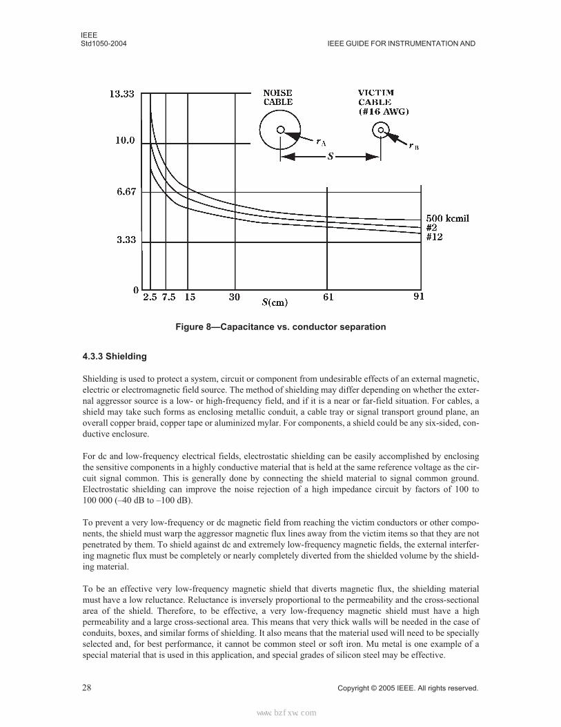
IEEEStd1050-2004 IEEE GUIDE FOR INSTRUMENTATION AND
4.3.3 Shielding
Shielding is used to protect a system, circuit or component from undesirable effects of an external magnetic,electric or electromagnetic field source. The method of shielding may differ depending on whether the exter-nal aggressor source is a low- or high-frequency field, and if it is a near or far-field situation. For cables, ashield may take such forms as enclosing metallic conduit, a cable tray or signal transport ground plane, anoverall copper braid, copper tape or aluminized mylar. For components, a shield could be any six-sided, con-ductive enclosure.
For dc and low-frequency electrical fields, electrostatic shielding can be easily accomplished by enclosingthe sensitive components in a highly conductive material that is held at the same reference voltage as the cir-cuit signal common. This is generally done by connecting the shield material to signal common ground.Electrostatic shielding can improve the noise rejection of a high impedance circuit by factors of 100 to100 000 (–40 dB to –100 dB).
To prevent a very low-frequency or dc magnetic field from reaching the victim conductors or other compo-nents, the shield must warp the aggressor magnetic flux lines away from the victim items so that they are notpenetrated by them. To shield against dc and extremely low-frequency magnetic fields, the external interfer-ing magnetic flux must be completely or nearly completely diverted from the shielded volume by the shield-ing material.
To be an effective very low-frequency magnetic shield that diverts magnetic flux, the shielding materialmust have a low reluctance. Reluctance is inversely proportional to the permeability and the cross-sectionalarea of the shield. Therefore, to be effective, a very low-frequency magnetic shield must have a highpermeability and a large cross-sectional area. This means that very thick walls will be needed in the case ofconduits, boxes, and similar forms of shielding. It also means that the material used will need to be speciallyselected and, for best performance, it cannot be common steel or soft iron. Mu metal is one example of aspecial material that is used in this application, and special grades of silicon steel may be effective.
Figure 8—Capacitance vs. conductor separation
28 Copyright © 2005 IEEE. All rights reserved.
标准分享网 www.bzfxw.com 免费下载
IEEECONTROL EQUIPMENT GROUNDING IN GENERATING STATIONS Std 1050-2004
Since the permeability of a magnetic material is not constant but depends on the flux density in the shieldmaterial, the magnetic flux density must be known in order to estimate the effectiveness of the shield used towarp the magnetic field away from the victim conductors contained within its enclosed volume. If the mag-netic flux density is so high that the magnetic shield becomes saturated, then the shield will not be effectiveabove the saturation point.
Effective very low-frequency magnetic field shielding is much more difficult to obtain than electrostaticshielding. For example, the effective magnetic shielding provided by enclosing a 60 Hz power cable in rigid,galvanized, steel conduit may only be a factor of 10 to 100 (–20 dB to –40 dB) for interfering frequenciesbelow 1 kHz. As the noise frequency increases, the effective shielding will increase.
The use of a shield to attenuate H-field interference (a near-field phenomena) on victim conductors in acable or similar circuit depends upon the shield operating in a fashion other than warping the magnetic fluxaway from the victim conductors or other component to be protected. In this second case, the magnetic fluxlines are allowed to penetrate the enclosing shield and to reach into the victim conductors without much (ifany) attenuation. This is achieved by grounding the shield at both ends, with the signal conductors containedinside the shield ground referenced to the same ground point as the shield at each end. The shield will thencarry an induced current from the aggressor H-field, and the contained victim conductors will also carry aninduced current from the aggressor H-field, with all of the induced currents being 180° out of phase with theaggressor current. Since the impedance of the shield’s closed loop (it is a larger mass of metal that is alsogrounded at both ends) is much lower than that of the signal conductors contained within (they are smallerand feed into circuitry), this allows more induced current flow to occur in the shield than in the signal con-ductors contained therein, so the shield’s current also develops its own magnetic field proportional to thecurrent flowing in it, and this is also closely coupled (it is an H-field) to the victim signal conductors alongwith the originally induced current from the aggressor source. Therefore, the shield’s magnetic field nowinduces its own current into the victim conductors with another 180° phase, thereby producing two currentflows in the victim conductors that are out-of-phase with one another. These two induced currents canceleach other out in the victim conductors, and what is left is the greatly attenuated “noise” on the victim cir-cuit, which cannot be removed without involving efforts with a diminishing rate of return for expendedeffort.
Note that the foregoing shielding effects are independent of the permeability or reluctance of the materialselected for the shield, but do depend upon its conductivity and surface area when skin-effect comes intoplay in the higher frequency ranges. If there are concerns about grounding the shield at both ends because oflow-frequency “ground loop,” then these will need to be addressed by the use of other methods. If there is noshield current induced by the aggressor H-field, then the shield cannot attenuate the EMI being induced intothe contained victim conductors. Also, twisting the victim conductors does not affect this situation since theproblem is one of induced CM current from the aggressor H-field and not a DM one.
Far-field shielding takes place by a different mechanism. When a high-frequency electromagnetic fieldimpinges on a conductive shield, most of the electromagnetic wave is reflected by the shield material byimpedance mismatch. A small portion of the wave is transmitted through the shield material and this isfurther attenuated as it travels through the thickness of the shield material. Thus, the field incident on theshielded circuit, component or system is lower than the incident electromagnetic field. A highly conductivematerial such as copper or aluminum, that is sufficiently strong enough to support itself, and encloses anentire circuit, will reduce interference from electromagnetic waves by factors of 10 000 to 1 000 000(–80 dB to –120 dB).
4.3.3.1 Electronic equipment shielding
Almost any metal cabinet is valued for electric field shielding because it bi-directionally helps prevent thecoupling of any electric fields in or out of the cabinet. The steel cabinet is valued for additional bi-direc-tional shielding from magnetic fields that may be generated in adjacent cabinets, or from within the subjectcabinet itself.
Copyright © 2005 IEEE. All rights reserved. 29
IEEEStd1050-2004 IEEE GUIDE FOR INSTRUMENTATION AND
For both the electric field and magnetic field shielding, cabinet openings or discontinuities may degrade theoverall performance, but seldom do they significantly alter the shielding performance. However, for electro-magnetic wave shielding, it must be remembered that the shield must totally enclose the protected circuit. Inthis case, the need for normal cabinet discontinuities, such as seams, cable penetrations, and apertures maysignificantly affect the shielding integrity of the cabinet and provide the possibility of electromagnetic cou-pling both in and out of the cabinet.
The efficiency of the electromagnetic wave coupling will depend upon the size of the hole or seam with rela-tion to the wavelength of the interference. Any opening in an enclosure can provide a highly efficientcoupling path at some frequency. As an opening increases in size, its coupling efficiency also increases.
An opening larger than λ/20 will permit electromagnetic energy to pass freely through the opening. There-fore, openings larger than λ/20 should be avoided. Since most EMI coupling problems are broadband innature, the wavelength must be that of the highest interference frequency. For a frequency of 100 MHz, themaximum dimension for a hole will be 0.15 m. For a frequency of 10 MHz, the maximum dimension will be1.5 m.
Any opening or seam without suitable EMI gasketing or special flange design that promotes capacitive cou-pling effects, and that is 1/2 λ or larger at the EMI’s frequency will allow maximum coupling of the EMI inor out of the shielded enclosure. Note that the sides of typical door openings on rack-type cabinets maytherefore represent vertically polarized slot-antennae with dimensions approaching two meters in somecases. Therefore, the tops and bottoms of these same doors may also represent similar horizontally polarizedslot-antennae with dimensions approaching one meter. A rack or other cabinet in which the door is left openduring operation represents a virtually unshielded volume.
Whenever an opening must be present in a cabinet, protective measures should be taken to reduce the threatof coupling. These protective measures include:
a) Keeping the longest dimension of apertures in cabinets less than λ/20. Openings larger than this willrequire additional protective measures.
b) Where cable must penetrate the cabinet through a hole, shielding can be accomplished by makingthe hole operate as a waveguide operating beyond cutoff frequency. This can be done by connectinga conductive tube to the inside of the cabinet as shown in Figure 9. Since the cutoff frequency of awaveguide is a function of twice the maximum width of the waveguide, the length of the conductivetube should be at least four times the width of the tube.
30 Copyright © 2005 IEEE. All rights reserved.
标准分享网 www.bzfxw.com 免费下载
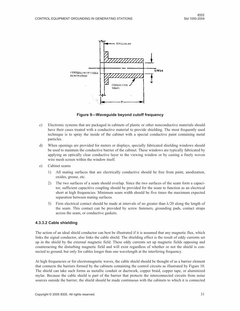
IEEECONTROL EQUIPMENT GROUNDING IN GENERATING STATIONS Std 1050-2004
c) Electronic systems that are packaged in cabinets of plastic or other nonconductive materials shouldhave their cases treated with a conductive material to provide shielding. The most frequently usedtechnique is to spray the inside of the cabinet with a special conductive paint containing metalparticles.
d) When openings are provided for meters or displays, specially fabricated shielding windows shouldbe used to maintain the conductive barrier of the cabinet. These windows are typically fabricated byapplying an optically clear conductive layer to the viewing window or by casting a finely wovenwire mesh screen within the window itself.
e) Cabinet seams
1) All mating surfaces that are electrically conductive should be free from paint, anodization,oxides, grease, etc.
2) The two surfaces of a seam should overlap. Since the two surfaces of the seam form a capaci-tor, sufficient capacitive coupling should be provided for the seam to function as an electricalshort at high frequencies. Minimum seam width should be five times the maximum expectedseparation between mating surfaces.
3) Firm electrical contact should be made at intervals of no greater than λ/20 along the length ofthe seam. This contact can be provided by screw fasteners, grounding pads, contact strapsacross the seam, or conductive gaskets.
4.3.3.2 Cable shielding
The action of an ideal shield conductor can best be illustrated if it is assumed that any magnetic flux, whichlinks the signal conductor, also links the cable shield. The shielding effect is the result of eddy currents setup in the shield by the external magnetic field. These eddy currents set up magnetic fields opposing andcounteracting the disturbing magnetic field and will exist regardless of whether or not the shield is con-nected to ground, but only for cables longer than one wavelength at the interfering frequency.
At high frequencies or for electromagnetic waves, the cable shield should be thought of as a barrier elementthat connects the barriers formed by the cabinets containing the control circuits as illustrated by Figure 10.The shield can take such forms as metallic conduit or ductwork, copper braid, copper tape, or aluminizedmylar. Because the cable shield is part of the barrier that protects the interconnected circuits from noisesources outside the barrier, the shield should be made continuous with the cabinets to which it is connected
Figure 9—Waveguide beyond cutoff frequency
Copyright © 2005 IEEE. All rights reserved. 31
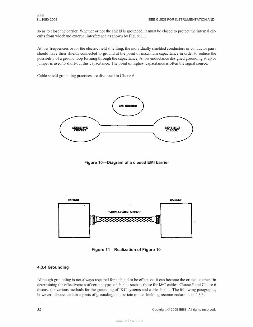
IEEEStd1050-2004 IEEE GUIDE FOR INSTRUMENTATION AND
so as to close the barrier. Whether or not the shield is grounded, it must be closed to protect the internal cir-cuits from wideband external interference as shown by Figure 11.
At low frequencies or for the electric field shielding, the individually shielded conductors or conductor pairsshould have their shields connected to ground at the point of maximum capacitance in order to reduce thepossibility of a ground loop forming through the capacitance. A low-inductance designed grounding strap orjumper is used to short-out this capacitance. The point of highest capacitance is often the signal source.
Cable shield grounding practices are discussed in Clause 6.
4.3.4 Grounding
Although grounding is not always required for a shield to be effective, it can become the critical element indetermining the effectiveness of certain types of shields such as those for I&C cables. Clause 5 and Clause 6discuss the various methods for the grounding of I&C systems and cable shields. The following paragraphs,however, discuss certain aspects of grounding that pertain to the shielding recommendations in 4.3.3.
Figure 10—Diagram of a closed EMI barrier
Figure 11—Realization of Figure 10
32 Copyright © 2005 IEEE. All rights reserved.
标准分享网 www.bzfxw.com 免费下载
IEEECONTROL EQUIPMENT GROUNDING IN GENERATING STATIONS Std 1050-2004
Ideally, no ac power or any other type of grounding conductor should penetrate an equipment cabinet with-out being appropriately filtered. When conductors do penetrate a cabinet, they can serve as a path alongwhich electromagnetic wave EMI can propagate and effectively reduce the shielding of a cabinet to 0 dB.Because this is a bi-directional situation, EMI from within the cabinet from the processing contained therein,will similarly be allowed to travel along the same conductor and to then EMI contaminate the overall envi-ronment. In this latter case the emissions compliance certification of the equipment can be voided. Thus, allpower wiring conductors must be interfaced to a cabinet or equipment enclosure via a fully shielded and LC-filtered wiring compartment, which topologically makes the power wiring appear to be on the cabinet’s out-side surface. Similarly, unless it is filtered, no grounding conductor must be allowed to penetrate the cabinet,but instead should be terminated directly to the outside surface of the cabinet before being allowed to makeentrance via a feed-through point. Most importantly, this also applies to cable shields.
At lower frequencies where either the electric field or the magnetic field coupling may be the source of EMIcoupling, the physical location of the grounding conductor can cause coupling to the conductors of sensitivecircuits. Since cable shields can be expected to pick up EMI, ground connections to this shield should bemade away from the conductors for sensitive circuits. The undesirable practice of using pig-tails or jumperwires to ground shields must be avoided for the additional reason that the pig-tails or jumpers provideunwanted coupling points to any victim conductors that may be parallel (or nearly so) oriented to them.
For cables entering or leaving a cabinet, the shields should be fully circumferentially grounded to the outsidesurface of the cabinet. For cables that run only internal to the cabinet, the shields should be low-inductancegrounded to the circuit common inside the cabinet. The use of pig-tails or jumpers should be avoided.
Proper shield grounding techniques will help to eliminate EMI noise radiation and reradiation from bothinternal and external sources, help to maintain the emissions compliance of the equipment, and help to min-imize any fire safety code issues.
4.3.5 Filters
All conductors penetrating an enclosure or cabinet are capable of bi-directionally conducting interferenceinto and out of the enclosure. This includes power conductors, grounding conductors, and any I&C cablesand associated cable shields. Once high-frequency noise enters a sensitive instrument, there is a good chancethat some portion of the high-frequency signal will appear as noise in the control circuits. In order for a filterto be effective, it is assumed that the interference frequency can be determined to be different than that of thesignal frequency and therefore out of the bandpass for the desired signal. Otherwise, attempts at filtering theEMI will also effect the desired signal process as well. This will occur for those portions of the signal thatoverlap in frequency or fall into the “skirt” area of the filter.
The worst case is when an EMI signal becomes impressed onto a digital system’s clock circuit since fromthere it may be routed throughout the system. This kind of EMI is also difficult to find since it makes itspresence known by being everywhere at the same time. The second worst case is when EMI enters a low-level amplifier circuit with sufficient bandwidth to amplify the EMI along with the desired signal. Thisraises the amplitude of the EMI signal to levels far above what it started out, and this allows it to become astronger source of EMI than it originally was. Proper filtering of circuits is used to generally minimize, if noteliminate, these problems along with others.
Many high-frequency transients can be prevented from entering control enclosures by bypassing each con-trol conductor to the signal/frame ground with a 0.1 microfarad ceramic disk capacitor at the terminal blockwhere the cable enters. This method is most effective if the bypass occurs on the outside surface of theequipment cabinet before any EMI can enter the cabinet’s volume. For this method to be effective, the leadsof the bypass capacitors should be kept as short as possible. Even better for purposes of bypassing is the useof a coaxial style feed-through capacitor that has its metal case solidly grounded to the equipment’s enclo-sure at the point of penetration. Care should be taken in evaluating if either of these methods will cause anundesirable time delay or waveform distortion of the signal.
Copyright © 2005 IEEE. All rights reserved. 33
IEEEStd1050-2004 IEEE GUIDE FOR INSTRUMENTATION AND
LC types of filters achieve their action on the EMI by the following interrelated actions:
1) Reflection via impedance mismatch reflects the EMI back up the same path from which it triedto enter the filter.
2) By circulating the EMI within the filter’s elements and creating EMI losses via heat dissipationin the filter’s components.
3) By low-impedance shunting action between conductors, and to equipment or signal groundconductors through filter components that are connected line-to-line and line-to-ground.
4) By radiation from the filter’s components into the environment (undesired) and to be mini-mized in a good filter design.
5) By letting the remaining EMI through the filter and out onto the filter’s other port.
If the EMI is common mode, the filter must be connected in series between each conductor (includingground conductors and shields) so as to raise the path’s impedance to CM current. More impedance equalsless current in the path, which results in EMI attenuation. Inductors may also be configured in CM to createa transformer bucking action between the CM current appearing on the conductors.
If the EMI is DM in nature, the filter must be connected between the signal conductors and additionally con-nected to signal or equipment ground depending upon the circuit being filtered.
Generally a combination filter is used that can attenuate both CM and DM noise. There are many types offilters, but the most common type is a simple combination inductor and capacitor, reactive filter configuredfor either high pass or low pass and with a characteristic impedance equal to that of the circuit into which itis to be placed at some specified center frequency. For ac power wiring, this is typically 50 Ω at 60 Hz andon telephone type circuits 600 Ω. The center frequency of the latter filter depends upon whether the type ofcircuit is voice grade or digital.
Filters can range anywhere from simple capacitors and ferrite beads used by themselves, to sophisticated,multi-stage and physically large bandpass filters. The configuration of the filter will naturally depend uponthe characteristics of the noise to be filtered, and the rms and peak currents of the signal to be passed throughthe filter in unattenuated fashion. Since different filter configurations will affect signal parameters such aspulse rise time and waveshapes of both digital and analog circuits, both the positive and negative effectsmust be considered when applying filters. Supplemental filters have also been known to cause detrimentalringing of digital circuits.
4.3.5.1 AC power filters
AC power line filters should preferably be of the hybrid common-mode/differential-mode type in order tocombat both types of conducted EMI. Power line filters should be located with regard to the followingconsiderations:
a) The filter should optimally be mounted in the bulkhead of the cabinet to protect against input-outputlead parasitic capacitance coupling at high frequencies. This is a serious problem that is often over-looked.
b) If the filter cannot be mounted on the bulkhead, isolate the unfiltered power leads to avoid recou-pling EMI to the nonfiltered power leads or to signal cabling.
c) Select a power line filter either with a high input impedance or to specifically match the load imped-ance to avoid changing the overall electrical characteristics of the power distribution system.
d) The power line filter should be rated for the appropriate line-to-line and line-to-ground workingvoltage and the number of phases on the circuit (including neutral if used).
e) The power line filter should be rated to handle the continuous rms current of the load, and any peakcurrents that the load may require.
34 Copyright © 2005 IEEE. All rights reserved.
标准分享网 www.bzfxw.com 免费下载
IEEECONTROL EQUIPMENT GROUNDING IN GENERATING STATIONS Std 1050-2004
f) The power line filter should be able to handle the harmonic currents from non-linear loads in addi-tion to the fundamental current from the load.
4.3.5.2 Filtering of grounding conductors
Since the equipment grounding conductor is also the conductor that the typical power entry low-pass LC fil-ter for electronic load equipment will be referenced to on an ac power system, its impedance must always bekept as low as possible. This allows the filter to successfully return EMI that it has shunted into the equip-ment ground to be effectively returned to the ac source. A beneficial EMI loop exists between the LC filterand the ac power source via the interconnecting equipment grounding conductor. Hence, a maximized EMIcurrent in this path may be viewed as beneficial if it is part of the LC filter’s operating mode. Accordingly,any actions taken to raise the impedance of this equipment grounding conductor path will have undesirableresults.
For example, if an inductance (“choke”) is placed into the equipment grounding conductor path for equip-ment that is attempting to use the path for LC filter return current, the action will reduce the effectiveness ofthe LC filter to the point that it will simply pass the EMI into the equipment it was intended to keep it out of.Placing an inductance into the path has the equivalent effect of adding it in series with the LC filter’s shuntcapacitors, which is a known poor practice.
However, if an inductance is inserted into the equipment grounding path for the LC filter, the indicationswill be that the equipment ground path is “quieter,” but that there is now an “unexplained” increase in theamount of CM EMI “noise” current that can be detected in the interconnecting cables from the victim equip-ment to other items of the overall system. What has happened is that the LC filter’s return current “noise”has not been reduced, it has been unknowingly rerouted. Accordingly, the equipment grounding conductorpath between equipment and the ac power source must always be configured to offer the lowest amount ofimpedance across the widest range of frequency possible if reliable operation of the system is to beexpected.
4.3.5.3 CM filtering
The appropriate place to apply CM chokes to decouple CM noise current paths, is on the actual data, signal,control, or other interface cable itself. Or, if a large enough choke can be obtained, it may be applied aroundall of the ac power conductors (line, neutral, and equipment ground) along with the involved conduit or race-way. These kinds of placements of a choke increase the CM impedance of the path and allow a concurrentreduction in CM current, which is usually a beneficial situation.
At high-frequencies, the physical point at which a CM choke is placed onto a conductor is critical. Inductorsrequire current to operate, not voltage. Hence, the chosen point must be a point of significant current flow inorder to obtain the needed H-field flux to excite the inductor and get a back-emf action. This means that thewavelength of any CW type of EMI needs to be considered and the choke placed at points on the standingwave that are current maximums, and not minimums. Traveling waves will intersect the choke no matterwhere it is placed.
Since CM chokes are inductors, they become very unwieldy and expensive as they are designed for lowerfrequency use. Hence, they are most practical in the high-frequency range. When applied to ac power systemconductors of any kind, they may also experience core saturation if the circuit is producing flux at dc, powersystem fundamental, or harmonic frequencies. This means special care must be taken in the design of thechoke’s core to avoid this kind of problem, or the use of very large cores.
Copyright © 2005 IEEE. All rights reserved. 35
IEEEStd1050-2004 IEEE GUIDE FOR INSTRUMENTATION AND
4.3.6 Other noise minimization techniques
4.3.6.1 Signal Isolation transformers
Isolation transformers can be used to block common-mode interference and dc signals. When both ends of asignal wire pair are fed by signal isolation transformers, the wires become isolated from dc and low-frequency ground potential differences in the terminal equipment. In practice, signal isolation transformersnormally are configured as solidly grounded, center-tapped devices so as to present a differentially balancedimpedance to ground and to enhance safety. Electrostatic shielding in the signal isolation transformer isimportant as an additional means of reducing CM currents and a subsequent CM to DM current conversion.
4.3.6.2 Power isolation transformers
An isolation transformer is defined as any transformer consisting of a separate primary and secondary wind-ing where they are not interconnected to form an autotransformer connection. Whether or not the isolationtransformer is grounded is not a part of the definition. In this context, a power isolation transformer is still an“isolation” transformer when its secondary winding is solidly grounded to the equipment grounding conduc-tor, equipment frame/enclosure, and any earth grounding electrode system.
When an isolation transformer is introduced into the electrical distribution system and its secondary isgrounded, it is referred to as a separately derived ac system. If, instead of grounding the secondary of an iso-lation transformer, it is interconnected with another solidly grounded ac system via a common neutral con-ductor run, the arrangement is correctly called a solidly interconnected ac system.
Since all ac systems in a facility should be solidly interconnected via a common equipment grounding con-ductor system and earth grounding electrode system, a power isolation transformer cannot provide an “iso-lated” ground to any equipment connected to their secondary. Instead, a power isolation transformer used tocreate a separately derived ac system can provide a new and local ac system and equipment ground pointthat is local to the isolation transformer and its served loads without the necessity to use only the servicegrounding point, which may be quite distant. It is important to note that a power isolation transformer is notused to form a truly “isolated” ground point.
Power isolation transformers may also be provided with electrostatic shields between the primary and sec-ondary windings for enhanced shielding effectiveness.
4.3.6.3 Ground current neutralizing transformers
Ground current neutralizing transformers can be used to eliminate the effects of inductive coupling orground potential rise associated with cables entering a generating station or run in parallel with the powertransmission lines. The inductive coupling will cause ground currents to flow when the I&C cables havemultiple connections to ground, either intentionally or unintentionally, from the stray capacitance betweenthe cables and ground.
To implement this method, all incoming I&C cables will pass through the neutralizing transformer andbecome separate secondary windings. The primary winding has the same number of turns as each of the sec-ondaries and is energized by the same induced potential rise as the cables. To achieve this, one end of theprimary circuit may be connected to the station ground and the conductor is run along the same path as theI&C cables with the other end connected to ground at a sufficient distance not to be affected by station faultcurrents. Thus, a voltage equal to the ground rise is induced in the control circuits and the ground risepotential is not present between the incoming cables and these circuit. This cancellation voltage can also begenerated separately.
36 Copyright © 2005 IEEE. All rights reserved.
标准分享网 www.bzfxw.com 免费下载
IEEECONTROL EQUIPMENT GROUNDING IN GENERATING STATIONS Std 1050-2004
4.3.6.4 Differential amplifiers
The use of differential amplifiers is an effective means of reducing common-mode noise. Even though thecommon-mode tolerance of most integrated circuit differential amplifiers is only a few volts, common-modevoltages of up to several thousand volts can be tolerated by using various attenuation schemes.
4.3.6.5 Increase the signal-to-noise ratio
Care must be exercised in using this method for, although it will reduce the induced noise in one region offrequency, it will cause an increase in noise in another region. Changing the circuit impedance to reduce thenoise induced by either a primarily inductive or capacitive source is subject to the same warning asincreasing the signal-to-noise ratio. Narrowing the bandwidth of a circuit is another way to affect the signal-to-noise ratio without changing its impedance.
4.3.6.6 Optically-coupled circuits
Signal circuits that use metallic paths for signal transport can be spot-converted to optically isolated circuitsin order to reduce the effects of CM potentials and currents on the circuits. This is accomplished by intro-ducing an appropriate converter into the path (usually at both ends), which includes a dielectric barrier thatis bridged by a light beam that is generated by an LED and received on the opposite side by a photo-sensi-tive transistor. Such circuits are called optically-coupled and may have dielectric withstand characteristics ofseveral kV at dc. As the signal frequency increases, the input-to-output reactive coupling may negate theattempted isolation.
Opto-couplers need to be shielded to protect their internal circuits from the effects of nearby EMI.
4.3.6.7 Fiber optic cables
Fiber optic cables are immune to the interference sources that plague standard current-carrying I&C cables.The input and output circuits of the fiber optic links are sensitive to EMI and typically need shielding fromlocal sources of EMI.
Fiber optic cables are often metal-clad to provide mechanical protection of the cable itself. Such a conduc-tive sheath can introduce EMI and especially lightning currents into equipment if the sheath is not solidlygrounded prior to its being interfaced to the terminating equipment at the cable’s ends. Ungrounded metalsheaths represent both a fire and shock hazard, particularly when they are routed between buildings or overlong vertical or horizontal distances in the same building. The safety concerns are for both lightning and acsystem ground-fault conditions.
Metallic fiber optic cable sheaths cannot be effectively insulated in order to avoid solidly grounding them.
4.3.6.8 Surge arresters
4.3.6.8.1 AC power circuits 400 volts and above
Surge arresters are a specially listed and defined class of devices intended to protect electrical circuits fromthe effects of conducted surge current. The most commonly available form of surge arrester is one that isconnected in shunt with the ac power conductors and equipment ground. These designs non-linearly clampthe voltage across their terminals in line-to-line and line-to neutral/equipment ground according to howmuch current is passed through them and what their wiring configuration has been chosen to be. If there is asufficient potential difference between the line(s) and equipment ground, they will then divert surge currentinto the grounding path.
Copyright © 2005 IEEE. All rights reserved. 37
IEEEStd1050-2004 IEEE GUIDE FOR INSTRUMENTATION AND
Surge arresters with typically not operate until several kV have appeared across their terminals and afteroperation they may limit surge voltage to the downstream wiring system to some lesser value, but still one inthe kV range. The let-through voltage and its associated current is also dependent upon the surge currentbeing conducted by the arrester and is generally a non-linear relationship. the let-through characteristics ofthe surge arrester are determined b both its design characteristics and its installation method.
Modern surge arresters typically are of the solid-state variety and do not contain and air-gaps. Air-gapdesigns are not desirable since they represent an operating variable that is affected by environmental condi-tions and manufacturing tolerances to a very great degree. Such gaps also tend to experience large changesin performance with each succeeding use as the gap erodes.
Gas-filled and gapped arresters are not desirable since they represent a near short-circuit to the ac power cur-rent once they have ionized. In some cases, the ionization may continue for several cycles and large amountsof ac power will be faulted through the device. This places great electro-magnetic stresses on all parts of theinvolved path and may lead to related electrical equipment failure. SCR based “crowbar” types of surgearresters pose similar problems and are therefore not generally useful in this application.
Since the surge arrester can carry large amounts of surge current with fast rates of current change, for arrest-ers provided in equipment it is advisable to route its conductors adjacent to the equipment enclosure. Allsurge arrester conductors should be routed to keep them away from any EMI susceptible conductors. Thisespecially applies to the surge arrester’s earth grounding electrode conductors.
4.3.6.8.2 AC power circuits below 400 V
Transient Voltage Surge Suppressors (TVSS) are devices intended to be applied on the building wiring acpower distribution system by attachment to switchboards, panelboards, and branch circuit outlet ends. Theycan be provided integral with equipment. The ratings of the TVSS must be commensurate with their point ofinstallation on the wiring system. See IEEE Std C64.41.
The most commonly available form of TVSS is one that is connected in shunt with the ac power conductorsand equipment ground. These designs non-linearly clamp the voltage across their terminals in line-to-lineand line-to-neutral/equipment ground according to how much current is passed through them and what theirwiring configuration has been chosen to be. If there is a sufficient potential difference between the line(s)and equipment ground, they will then divert surge current into the grounding path; otherwise, they will not.
Series connected and hybrid designs must be rated to handle the full rms current on the circuit plus remainundamaged by available fault-current during short-circuits. This latter set of requirements limits the applica-tion of the TVSS to smaller ampacity circuits due to the high costs associated with the series or hybriddesign.
The most commonly available TVSS is MOV based, but may also contain items such as capacitors andstrings of matched avalanche diodes, which are series connected due to voltage breakdown requirements.Gas tube based and SCR “crowbar” types of designs on ac power circuits are generally avoided because ofthe same kinds of problems as discussed above with surge arresters used on service entries and equipment.
4.3.6.8.3 I&C circuits
TVSS equipment should be attached to I&C circuits that enter/exit a building or defined zone to preventthese circuits from propagating a lightning or fault current hazard into or out of the area.
MOV based TVSS designs are not normally used on data/signaling/telecommunications circuits where thecapacitance loading effects of the MOV would affect the waveform of the transmitted current on the circuit.LCR based TVSS designs are more accurately classified as filters and so are not discussed in this subclause.
38 Copyright © 2005 IEEE. All rights reserved.
标准分享网 www.bzfxw.com 免费下载
IEEECONTROL EQUIPMENT GROUNDING IN GENERATING STATIONS Std 1050-2004
Most common TVSS designs that are intended to provide maximum amounts of protection for the circuits towhich they are attached use hybrid arrangements. These are TVSS designs that incorporate both a (shunt)gas-tube, a series impedance, and a (shunt) Tranzorb connected into each of the circuit conductors and toground.
The avalanche diode is the first (and sometimes only) protective device to go into operation if the surge issmall. However, when the surge is larger, it works against the IZ drop the current develops across the seriesimpedance (usually a resistor). This both limits the current through the avalanche diode and ramps up thevoltage across the gas-tube on the impedance’s input side. The avalanche diode and resistor continue tooperate in unison until the ionization voltage for the gas-tube is reached, at which time the tube fires, andreduces the potential across its terminals to about 15 V. This then relieves the resistor and avalanche diodefrom the high-current handling task, but the avalanche diode may continue to conduct to some degree.
As a result of problems involved with obtaining an exact ionization and conduction condition in separategas-tubes, the design has evolved to use a common gas-filled envelope, which contains multiple electrodesthat are normally insulated from one another. Thus, when any surge causes any ionization to occur on anyelectrode, the whole gas-tube operates and with a constant voltage drop across each circuit. This importanteffect also minimizes the highly unwanted conversion of CM surge current to DM surge current. Most gas-tubes are photo-sensitive and so when installed, should be kept in enclosures designed to exclude light.
Hybrid TVSS designs are available in balanced and unbalanced circuit types and for a wide variety of circuitimpedances and protocols.
4.3.7 Summary of EMI minimization techniques classified by coupling mechanism
It should be noted that, in real-world applications, the selected EMI minimization techniques will need to beoptimized based on the type of interference encountered. Accordingly, some of the techniques that followare at odds with each other since each is optimized to reduce a specific coupling mechanism.
4.3.7.1 Common impedance coupling
a) Eliminate as many common impedance points between circuits as possible by not using any conduc-tor as part of more than one circuit and by not connecting the circuit signal return to ground frommore than one point.
b) Avoid using the equipment ground system as part of the signal return path. Where it is necessary touse the equipment ground system as part of the signal return path, make ground connections as shortand of as low an impedance as possible. This typically requires that the I&C conductor and groundsystem be close together.
c) Do not use the earth as a path for any signals or in an attempt to equalize potential between equip-ment or signal processes, particularly when ac power system ground-faults or lightning currentscould become involved. The earth is too high of an impedance to permit this and the level of itsimpedance rises with the frequency of the current. Ultimately, it becomes too high to be of any use.This typically occurs below 1 MHz.
Most earth ground testing occurs at or near dc to 1 kHz and the test results are “corrected” to showequivalent dc ohms. Hence, what appears to be a “good” 1 Ω earth ground is in reality a connectionof high ohmic value at just a few kHz. In addition to this, the impedance value of any conductorused to make the connection to the earth ground may be in the kilo- to meg-ohm range at the EMIfrequency of interest. This means that even if the earth ground would be a good connection byitself, the impedance exhibited by the conductor used to connect to it could invalidate the design.
d) Use signal reference ground planes or grids to equalize potential between interconnected items ofequipment over a very broad range of frequency. Typically these kinds of broad-band signal refer-ence structures (SRS) will be effective from dc to over several tens of MHz. The SRS also functions
Copyright © 2005 IEEE. All rights reserved. 39
IEEEStd1050-2004 IEEE GUIDE FOR INSTRUMENTATION AND
independently from earth ground, although for safety it must be connected to the facility groundsystem.
4.3.7.2 Capacitive coupling
a) Reduce the impedance of the sensitive circuit to load-down the capacitive coupling mechanism.
b) Position and connect conductive shields so that capacitively coupled noise currents are returned tothe signal common ground without flowing through the signal lines. Capacitive shields shouldadequately enclose the signal circuits and be constructed of a low-impedance material in order toprovide an alternative bypass path for the noise current. Use low inductance techniques in how theshield is connected to the ground reference.
c) Route control circuits to minimize coupling between high level circuits and low level circuits. Oth-erwise, effectively enclose one or the other, or both of the circuits in a shield that is effective for thekind of EMI being propagated from the aggressor to the victim circuit.
d) Specify transformers that have solidly grounded electrostatic shields provided between the primaryand secondary windings.
4.3.7.3 Inductive coupling
a) Increase the impedance of the sensitive circuit so that EMI current flow is reduced.
b) Divert dc and very low-frequency sourced magnetic fields by shielding them, the victim circuits, orboth with low reluctance (high permeability), ferrous material. Avoid letting this material becomesaturated.
c) Route control circuits to minimize coupling and loop area (physical separation, right angle crossing,radial routing, twisting of signal pairs).
d) Increase the rise time of the signal.
4.3.7.4 Radiation coupling
a) Absorb radiated waves by using a lossy dielectric or magnetic shield.
b) Reflect radiated waves by using metallic shields.
c) Separate the emitter and receiver by the maximum possible distance since radiated power strength isinversely proportional to the square of the distance. The E-field component of the radiated signalwill be inversely proportional to the linear distance.
d) Design cabinet openings with regard to the techniques presented in 4.3.3.1.
e) Terminate external cable shields and power or signal filter grounds on the external surface of thecabinet via fully circumferential connections. Do not use “pig-tail” type connections or jumpers.
f) Recognize and prevent the pickup of electromagnetic radiation near the emitter by inadvertentantennas/conductors and the propagation of that wave to areas near the receiver where it can be re-radiated.
4.3.7.5 Common-mode rejection techniques
Common-mode noise can be produced by any of the above four coupling methods. Since common-modenoise is often converted into differential-mode noise, common-mode noise is the most frequent source oftrouble within I&C circuits. Several techniques that are useful in minimizing common-mode noise are:
a) Make the signal circuit symmetrical by using a balanced transducer and identical signal lines.
b) Minimize the common-mode coupling by increasing the physical separation between the emitter andthe receiver and minimizing the number of direct connections to the interference source.
c) Use shielding techniques to prevent the interference from reaching the sensitive circuits.
40 Copyright © 2005 IEEE. All rights reserved.
标准分享网 www.bzfxw.com 免费下载
IEEECONTROL EQUIPMENT GROUNDING IN GENERATING STATIONS Std 1050-2004
d) Use common-mode rejection devices such as differential amplifiers, power or signal isolation trans-formers, optical isolators, and CM chokes.
e) Utilize proper grounding methods.
Below 30 kHz and perhaps to as much as 300 kHz, apply the concepts of single-point grounding and floatinglogic or signal grounds while avoiding multiple grounding connections to the circuit common. This may bedifficult to achieve in an extensive system.
Above 30 kHz and below 300 kHz, multi-point grounding may be beneficial. However, above 300 kHz,multi-point grounding is required and extensive use of ground reference structures such as planes, grids, orboth should be made. When processes exist on the same system that employ bandwidths above and below30, then multi-point grounding must be used in combined, hybrid fashion with single-point grounding.
5. I&C system grounding
5.1 Grounding philosophy
5.1.1 Principal objectives
The principal objectives of generating station grounding practices are to:
a) Maintain safe voltages across the station area during high-voltage system transients (step and touchpotentials).
b) Minimize the effects of lightning surges on equipment and structures.
c) Provide a low-impedance, ground fault current return path.
d) Provide a low-impedance leakage path for any static charge that might accumulate on equipment.
e) Minimize noise interferences in I&C systems by providing a broad-band, common signal referenceof low relative impedance between devices, circuits, and complete systems.
Grounding circuits often share multiple functions, and it is necessary to design a grounding network so thatthe conveyance of transient voltages from electrical faults, lightning strikes, etc., does not interfere with thefunction of minimizing noise and preventing these transients from impinging on circuit elements beyondtheir limit of transient immunity. All portions of the station ground system, whether for power, lightning, orsignal reference, need to be interconnected and should not be isolated from each other for any reason. Iso-lated grounding elements represent a safety and operational hazard as discussed in 5.2.1.
It is therefore necessary to recognize the following four points: The first is that all points on the earth (evenwithin relatively close proximity) will not be the same or equal potential relative to an arbitrary referencepoint for all frequencies. The second is that each element of a grounding network has a finite resistance andimpedance. The third is that there is an inherent transient susceptibility of discrete circuit elements. Caremust therefore be taken to ensure that the environment will not exceed the specific operating limits of theindividual circuit elements. The fourth is that as local transients cause ground potentials to reach high val-ues, currents may enter conductively connected cable circuits and may also be capacitively and inductivelycoupled from grounded cable shields in the affected area into the I&C conductors. These conductors mayterminate outside of the transient area and could impress high voltages on any connected equipment, withthe possibility of causing equipment damage, personnel hazards, or fire hazards.
Copyright © 2005 IEEE. All rights reserved. 41
IEEEStd1050-2004 IEEE GUIDE FOR INSTRUMENTATION AND
5.1.2 Generating station grounding system
In any generating station there are four identifiable grounding systems which are all tied to the stationgrounding grid. Those for lightning, station service power, and equipment grounding are discussed in thefollowing references:
a) IEEE Std 665-1995
b) IEEE Std 142-1991
c) IEEE Std 1100-1999
Requirements of local safety codes are discussed in Annex B.
The fourth grounding system, discussed in the following subclauses, is the I&C grounding system, which isdesigned to minimize the generation and transfer of noise voltages.
5.2 Types of signal ground systems
An electronic I&C system may be viewed as a complex hub consisting of one or more microprocessors andnumerous I&C circuits interfacing through cables with end devices. Within the hub, the interconnectionsmay be complex and it may be impossible to use individual return paths for each end device. Therefore, acommon ground or reference plane may be created that will individually act as a return path for one group ofsignals. Ideally, this reference plane would offer zero impedance to all of the signals it serves. If this werethe case, all of the individual signal currents within this system would return to their respective sourceswithout creating unwanted coupling and interference. It is, however, impractical to achieve zero impedanceconnections, so care must be exercised in interfacing this system to the rest of the plant grounding systems.Improper grounding may cause the flow of electrical noise currents in these common signal returns and cre-ate problems. The majority of signals in generating station I&C systems are dc or low-frequency signals.
A fundamental objective of a separate signal ground system is to achieve the same safety goals as the equip-ment safety ground system, but to do so while keeping the electrical equipment safety ground conductorsseparate from I&C ground conductors. The separation is desired in order to minimize EMI coupling fromelectrical equipment, which may have high levels of EMI that could interfere or damage sensitive I&Cequipment. There are three common approaches toward this—single-point grounding, multiple-pointgrounding, and floating grounds. Each concept has its advantages and disadvantages, and a typical generat-ing station signal ground system may use a combination of all three, but in no case shall a method be imple-mented in such a manner as to create a personnel or fire hazard.
An important element of determining which type of grounding method to utilize is the operating frequencyof the I&C system. While the actual microprocessor frequency within an equipment cabinet would be con-sidered high frequency, the vast majority of I&C circuits that exit the cabinets are dc or low-frequency. Theinherent conflicts in grounding philosophies for high- and low-frequency circuits has been a continuingsource of confusion in determining the proper grounding techniques for I&C systems. The preponderance oflow-frequency circuits in generating station I&C systems generally utilize the single-point grounding tech-niques, which are often recommended by equipment manufacturers.
Note that Figure 12, Figure 13, Figure 14, and Figure 15 depict an additional local supplementary groundconnection to a local grounding system for each cabinet in addition to the equipment grounding conductorprovided with the incoming ac power circuit. This additional connection will enhance personnel safety byensuring near-zero step and touch potential to nearby equipment. For some figures, this local groundconductor has also been shown extended to the station ground grid as this optional connection may be rec-ommended by equipment vendors.
42 Copyright © 2005 IEEE. All rights reserved.
标准分享网 www.bzfxw.com 免费下载
IEEECONTROL EQUIPMENT GROUNDING IN GENERATING STATIONS Std 1050-2004
5.2.1 Single-point ground system
The single-point ground system is principally used to reduce the unwanted circulation of both dc and acpower system related fundamental and harmonic ground currents in the signal grounding paths. These cur-rents may cause common-mode noise across the range from 0 Hz to about 6 kHz (the 100th harmonic of60 Hz). A single-point ground system is implemented by connecting the signal circuit common to the stationground reference from only one point. This grounding method is very effective and adequate when dealingwith equipment operating at frequencies below 30 kHz and not exceeding 300 kHz. Various sources placethis frequency at anywhere between 100 kHz and 10 MHz. The equipment manufacturer should be con-sulted for each specific installation.
The signal ground reference point should be tied to the equipment safety ground point within the enclosureor local area and there should be no more than one (preferably filtered) ground lead exiting each equipmentenclosure. This lead should be a stranded and insulated conductor sized to minimize the steady-state poten-tial difference between devices (less than 1 V or manufacturer’s recommendation), and to meet the requiredmechanical strength. However, under conditions of high magnetic fields (Ldi/dt) this conductor will not nor-mally be able to meet the previous requirement for potential equalization unless the rate of current changeper ampere is quite low. Hence, it is normally not very useful in controlling transient current induced poten-tial differences between its ends.
The I&C ground points of each cabinet should be connected by insulating cables to a common insulated bus.The insulated ground conductors serve not only to galvanically isolate the signal ground from unintentionalgrounds but also to easily differentiate them from the equipment safety ground conductors. A single insu-lated connection is then made from the common signal ground to the interconnected generating stationgrounding system. Use of isolated ground rods as the reference point is a safety hazard because the isolatedground reference does not have a direct connection back to the power system neutral which could preventprotective devices from operating because of the high impedance which is introduced. Equipment misopera-tion and damage from transients and lightning can also become more likely since the isolated reference willhave a much larger voltage difference during the transient event than the other interconnected elements. Allparts of the grounding system need to be interconnected at some point. Additional discussion is contained inIEEE Std 142-1991 and IEEE Std 1100-1999.
A separate I&C grounding system should be utilized within the cabinet enclosure and it is advantageous tokeep these conductors separate from the power or equipment safety grounding connections. Adjacent cabi-nets should be bolted or bonded together with a single strap or cable for the group. This connection is inaddition to the equipment safety grounding conductor or conduit/raceway provided with the incoming acpower circuit. Cabinets located close together should have the supplementary grounds tied together at a sin-gle reference point in the local area.
Single-point grounding design is primarily based on the prevention of dc and very low-frequency groundcurrents from flowing in the signal common. Because electrical power equipment contributes most of theground current, it is good practice to keep the grounds for sensitive equipment away from power circuits andtheir ground return paths where large leakage or fault currents may occur. The equipment ground for a cabi-net containing I&C equipment should be recognized as being different from the equipment ground for a 400or 480 volt motor control center in regards to EMI, but not for safety. It is normally not good practice to tiethe signal or cabinet grounds from an I&C cabinet to the same point as the equipment grounds for equipmentsuch as motor control centers because of the higher possible currents during both normal system operationand system transients.
A disadvantage of the single-point grounding system is that it may fail to function as a signal reference andeven may be detrimental at high operating or threat frequencies. As equipment dimensions or ground con-ductor lengths ultimately approach 0.15, the conductor can no longer be considered a low-impedance con-ductor. In this manner, the signal grounding conductor will not effectively act to equalize potential betweenits ends and may carry EMI to or from the system and increase any interference problems. Single-point
Copyright © 2005 IEEE. All rights reserved. 43
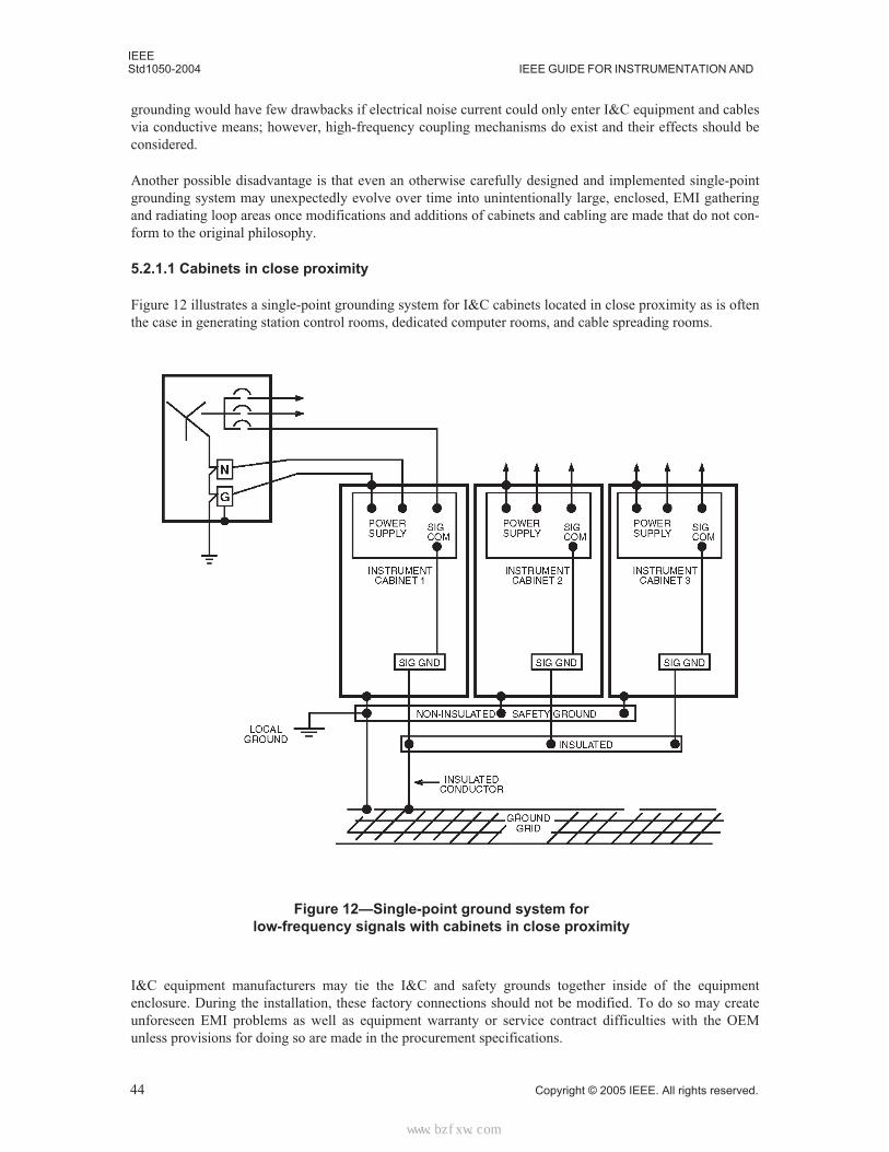
IEEEStd1050-2004 IEEE GUIDE FOR INSTRUMENTATION AND
grounding would have few drawbacks if electrical noise current could only enter I&C equipment and cablesvia conductive means; however, high-frequency coupling mechanisms do exist and their effects should beconsidered.
Another possible disadvantage is that even an otherwise carefully designed and implemented single-pointgrounding system may unexpectedly evolve over time into unintentionally large, enclosed, EMI gatheringand radiating loop areas once modifications and additions of cabinets and cabling are made that do not con-form to the original philosophy.
5.2.1.1 Cabinets in close proximity
Figure 12 illustrates a single-point grounding system for I&C cabinets located in close proximity as is oftenthe case in generating station control rooms, dedicated computer rooms, and cable spreading rooms.
I&C equipment manufacturers may tie the I&C and safety grounds together inside of the equipmentenclosure. During the installation, these factory connections should not be modified. To do so may createunforeseen EMI problems as well as equipment warranty or service contract difficulties with the OEMunless provisions for doing so are made in the procurement specifications.
Figure 12—Single-point ground system for low-frequency signals with cabinets in close proximity
44 Copyright © 2005 IEEE. All rights reserved.
标准分享网 www.bzfxw.com 免费下载
IEEECONTROL EQUIPMENT GROUNDING IN GENERATING STATIONS Std 1050-2004
5.2.1.2 Cabinets that are widely separated
In a distributed I&C system, the equipment cabinets may be located throughout the generating station and itis impractical or poor practice to implement the single-point grounding arrangement of Figure 12. Physicallydistributed systems often take the form of a primary control system such as that of Figure 12, with additionalremote input/output cabinets from the same manufacturer, as well as interfaces to other control system pack-ages from different manufacturers. An I&C system is considered a distributed system when the individualcontrol station cabinets are separated from each other by a distance long with respect to the wavelength ofthe interfering signal, but still not at a high enough frequency to create an electromagnetic wave. Separationdistances of 30 m between cabinets may be sufficient for them to be electrically “widely separated.”
Such as system has special problems since the cabinet ground points will be at relatively different potentialswith respect to each other, and unwanted currents may then flow on any ground connection between thecabinets. Figure 13 illustrates an approach to this situation by creating a separate single-point grounding sys-tem for each geographic grouping of equipment.
In utilizing multiple, single-point ground systems, the interconnection of low-frequency I&C cables betweenthe separate groupings should be avoided. Connections between widely separated cabinets should be high-frequency data highway cables. The communications circuits between the cabinets must have appropriateprotection for the common-mode noise, which is likely to result from the impedance of the long, insulatedsignal grounds. Standard common-mode protection ratings may not be adequate unless the requirements arebuilt in to the procurement specification. Signals between systems should use either differentially connectedsignal isolation transformer coupling or ac capacitor coupling with transmitter/receiver circuits having acommon-mode withstand voltage that safely exceeds the ground voltage under fault conditions. It may bepreferable to eliminate all metallic signal paths between the widely separated cabinets by the use of by fiberoptics, optical-coupling means, or by using wireless communications at infra-red or radio frequency.
Copyright © 2005 IEEE. All rights reserved. 45
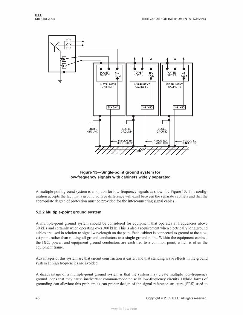
IEEEStd1050-2004 IEEE GUIDE FOR INSTRUMENTATION AND
A multiple-point ground system is an option for low-frequency signals as shown by Figure 13. This config-uration accepts the fact that a ground voltage difference will exist between the separate cabinets and that theappropriate degree of protection must be provided for the interconnecting signal cables.
5.2.2 Multiple-point ground system
A multiple-point ground system should be considered for equipment that operates at frequencies above30 kHz and certainly when operating over 300 kHz. This is also a requirement when electrically long groundcables are used in relation to signal wavelength on the path. Each cabinet is connected to ground at the clos-est point rather than routing all ground conductors to a single ground point. Within the equipment cabinet,the I&C, power, and equipment ground conductors are each tied to a common point, which is often theequipment frame.
Advantages of this system are that circuit construction is easier, and that standing wave effects in the groundsystem at high frequencies are avoided.
A disadvantage of a multiple-point ground system is that the system may create multiple low-frequencyground loops that may cause inadvertent common-mode noise in low-frequency circuits. Hybrid forms ofgrounding can alleviate this problem as can proper design of the signal reference structure (SRS) used to
Figure 13—Single-point ground system for low-frequency signals with cabinets widely separated
46 Copyright © 2005 IEEE. All rights reserved.
标准分享网 www.bzfxw.com 免费下载
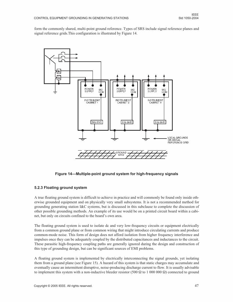
IEEECONTROL EQUIPMENT GROUNDING IN GENERATING STATIONS Std 1050-2004
form the commonly shared, multi-point ground reference. Types of SRS include signal reference planes andsignal reference grids.This configuration is illustrated by Figure 14.
5.2.3 Floating ground system
A true floating ground system is difficult to achieve in practice and will commonly be found only inside oth-erwise grounded equipment and on physically very small subsystems. It is not a recommended method forgrounding generating station I&C systems, but is discussed in this subclause to complete the discussion ofother possible grounding methods. An example of its use would be on a printed circuit board within a cabi-net, but only on circuits confined to the board’s own area.
The floating ground system is used to isolate dc and very low-frequency circuits or equipment electricallyfrom a common ground plane or from common wiring that might introduce circulating currents and producecommon-mode noise. This form of design does not afford isolation from higher frequency interference andimpulses once they can be adequately coupled by the distributed capacitances and inductances to the circuit.These parasitic high-frequency coupling paths are generally ignored during the design and construction ofthis type of grounding design, but can be significant sources of EMI problems.
A floating ground system is implemented by electrically interconnecting the signal grounds, yet isolatingthem from a ground plane (see Figure 15). A hazard of this system is that static charges may accumulate andeventually cause an intermittent disruptive, noise-producing discharge current to flow. It is usually advisableto implement this system with a non-inductive bleeder resistor (500 Ω to 1 000 000 Ω) connected to ground
Figure 14—Multiple-point ground system for high-frequency signals
Copyright © 2005 IEEE. All rights reserved. 47
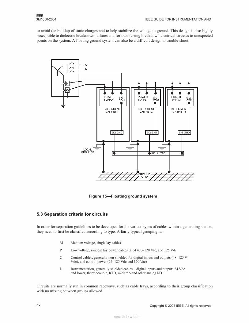
IEEEStd1050-2004 IEEE GUIDE FOR INSTRUMENTATION AND
to avoid the buildup of static charges and to help stabilize the voltage to ground. This design is also highlysusceptible to dielectric breakdown failures and for transferring breakdown electrical stresses to unexpectedpoints on the system. A floating ground system can also be a difficult design to trouble-shoot.
5.3 Separation criteria for circuits
In order for separation guidelines to be developed for the various types of cables within a generating station,they need to first be classified according to type. A fairly typical grouping is:
Circuits are normally run in common raceways, such as cable trays, according to their group classificationwith no mixing between groups allowed.
M Medium voltage, single lay cables
P Low voltage, random lay power cables rated 480–120 Vac, and 125 Vdc
C Control cables, generally non-shielded for digital inputs and outputs (48–125 V Vdc), and control power (24–125 Vdc and 120 Vac)
L Instrumentation, generally shielded cables—digital inputs and outputs 24 Vdc and lower, thermocouple, RTD, 4-20 mA and other analog I/O
Figure 15—Floating ground system
48 Copyright © 2005 IEEE. All rights reserved.
标准分享网 www.bzfxw.com 免费下载
IEEECONTROL EQUIPMENT GROUNDING IN GENERATING STATIONS Std 1050-2004
In determining the required separation between the cables, the raceway method utilized effects the minimumseparation distance. For cables routed in metallic conduits, the separation distances would be less for mag-netic conduit than for aluminum conduit. Separation required between metallic conduits will also generallybe less than the separation required for cables trays, particularly ladder-type trays with no covers. For cablesrouted in trays, a separation distance of 50 cm is normally maintained for installation purposes, and this isgenerally a sufficient distance between categories P and L (with solid bottoms and covers), with 25 cm beingrequired between categories P and C. A distance of 120 cm would be recommended between categories Mand L. When trays are installed vertically stacked by group as listed above, the recommended separation dis-tances can often be readily achieved. Barriers within a tray can also be utilized for separation the differentcable types.
When conduit is utilized, cables of Group L should normally be run in magnetic conduit to provide optimumshielding. When each of the circuit groups is run in a common underground duct bank where wide separa-tion distances are not feasible, magnetic conduit should continue to be utilized for the circuits of Group L.
Not all of the above grouping will be found in every installation, while other groupings and separations maybe required for data communication, fire protection, and telephone cables. Separation criteria can be a rela-tively simple set of guidelines, or it can be expanded into an elaborate set of tables to cover numerous instal-lation conditions.
Some vendors have specific raceway and separation criteria for the cables associated with their equipment,and these should be incorporated into the overall project separation criteria.
5.4 I&C system power considerations
The following considerations should be taken into account when designing the grounding system for a cen-tralized I&C system similar to that shown in Figure 12.
a) All ac power circuits should come from one locally installed source that is separately derived or sol-idly interconnected such as a UPS or an isolation transformer.
b) Each ac power circuit should contain an equipment ground conductor that connects to the equipmentframe and references it to the power source.
c) AC power should be distributed from the local power source to all local cabinets in the systemthrough individual circuit breakers or fuses. Each circuit should be a dedicated, individual load.
Note that some existing generating stations may use an ungrounded (floating) ac power distribution systemfor their I&C systems, while other utilize a grounded system. Only the latter design utilizes the equipmentground connection for ac fault protection on the first ground fault to occur. The floating design requires twoground faults to occur before the protective equipment can operate. Floating ac power distribution systemsare not recommended unless extensive use is made of ground fault detectors and alarms for the first faultoccurrence. Ungrounded systems are also difficult to achieve in practice as many equipment internal powersupplies ground one end of the output to the power supply frame, which is in turn solidly connected to theequipment frame and ground.
5.5 Surge protection considerations
5.5.1 Power supply circuits
Experience has shown that the I&C system power source can be a significant source of EMI problems.Surge protection should be provided for all incoming power feeds to critical I&C systems. Many vendorsrecommend that their equipment be fed from a dedicated local, separately derived power source. Since thisis most commonly a UPS or isolation transformer, both of these devices provide some inherent degree ofsurge protection. Subclause 4.3.5.1 contains recommendations on the use of ac power filters.
Copyright © 2005 IEEE. All rights reserved. 49
IEEEStd1050-2004 IEEE GUIDE FOR INSTRUMENTATION AND
5.5.2 Instrumentation and control circuits
Operating experience has shown that, in general, surge protection is not required for I&C circuits locatedwithin the main “powerhouse” of traditional steam turbine generating stations and that control circuits thatterminate outside of the powerhouse at outlying facilities such as circulating water pumphouses, fuel oilstorage, water treatment, etc. may become likely source of surges, which can cause equipment misoperationor damage.
IEC 61312-1:1995 discusses a “zone concept” that elaborates on the empirical findings noted above. Sepa-rate geographic “zones” are identified working outwards from the control system, and surge protectionshould be provided whenever a circuit crosses a zone boundary. The goal is to have high capacity surge pro-tective devices mitigate the surge closest to its point of origin external to the generating station, and thenhave subsequent surge mitigation with tighter voltage clamping levels and lower energy ratings at each zoneboundary heading into the main I&C system processors. Providing surge protection only at either or bothends of a long I&C circuit terminated outside of the main generating station building has been found to beinsufficient in some cases. Intermediate surge protection, as discussed by the “zone method,” is a logicalframework for providing enhanced surge protection. Providing surge protection at boundaries such as exit-ing a building as meshes well with certain national codes such as discussed in Annex B.
5.6 Other grounding considerations
5.6.1 Equipment safety grounds (mechanical, frame)
The equipment in this context is the exterior housings of I&C systems. Specifically, it refers to normallynon-current-carrying metal enclosures, such as cabinets, frames, and racks. The major objective of theequipment safety ground is to prevent hazardous potentials from developing between adjacent groundedequipment in order to protect personnel and equipment against hazards posed by electrical power transientsand faults. A desired objective of the equipment safety ground is to provide a low-impedance path for acsystem fault currents.
Requirements for the design and installation of an equipment safety ground include:
a) Ensure that all enclosures are constructed with special provisions, such as a designated equipmentcabinet ground stud, lug, or bus for terminating the ac equipment grounding conductor that is runwith the input power cable from the power distribution system. This connection is in addition to thesolid bonding of any metal armor, conduit, or raceway provided with the incoming ac power con-ductors. A continuous metallic raceway system of sufficient ampacity may serve as the ac equip-ment grounding conductor. Connect the ac equipment ground conductor and/or continuous metallicraceway system to the designated equipment safety ground bus for the cabinet.
b) Provide a supplementary ground cable connection to the cabinet. The supplementary ground cable isnot run with any ac power circuit conductors and will connect to the closest local ground point,ground mat, or reference ground plane if one is available. If multiple enclosures are physicallygrouped together, first bond them by bolting them to one another and then use only one connectionbetween the enclosure group and the supplementary ground. This singular supplementary groundconnection is in addition to the ac equipment grounding conductor and/or continuous metallic race-way system provided with the incoming ac power circuit to each cabinet. The supplementary groundcable should be a flexible, stranded conductor. This conductor should only be insulated if corrosionis a severe hazard. In known corrosive environments, periodic checks should be made as to theintegrity of all ground connections.
5.6.2 Ground conductor lengths
At MHz signal frequencies, the impedance of a single conductor can become high enough so that it nolonger provides a grounding connection between two points for the purpose of equalizing the relative poten-
50 Copyright © 2005 IEEE. All rights reserved.
标准分享网 www.bzfxw.com 免费下载
IEEECONTROL EQUIPMENT GROUNDING IN GENERATING STATIONS Std 1050-2004
tial of those points. For example, a conductor that represents an impedance of less than 0.3 Ω at 60 Hz willrepresent over 40 000 Ω at 10 MHz. Ground conductors longer than 1 m may be viewed as detrimentalrather than beneficial for dealing with EMI frequencies in the MHz range.
5.6.3 Generating station-to-substation interconnect
Although not installed for I&C circuit reasons, large diameter ground cables are usually installed along theinterconnecting ducts banks and cable trenches between a generating station and its switchyard. In general,conductors equal in size to the ground grid conductors should be installed either along the top corners of aduct bank or near both upper, inner sides of cable trenches. These cables should be bonded to both the gen-erating station and substation ground grids as well as to ground rods at intermediate points. Similarly, buriedcounterpoise conductors underneath the transmission lines between the substation and generating stationwill provide additional ties between the grounding systems.
Determining the size of these grounding conductors is related to the required I2t current handling character-istics and not its impedance at high-frequency for EMI control purposes. Achieving a low impedancerequires a focus on surface area and length-to-width ratio rather than on cross-sectional area for fault-currentcapability and mechanical robustness.
As a result of the coupling actions of the magnetic fields involved between these grounding conductors andthe plant’s ac power system conductors that are related to them, they will generally provide a lower imped-ance path than the I&C cable shields will. Therefore much, but not all, of the ground-fault currents from theac system may be diverted from the I&C cables. These grounding conductors also help to safely limit theground step and touch potential differences between the two grids during transients from lightning andfaults.
5.6.4 CT, VT, and CCVT grounding
Within IEEE Std C57.13.3-1983, much has been written and standardized about the proper techniques to usewhen grounding these devices. The general consensus is that the secondary neutrals for these devices shouldbe grounded at the entrance to the relay room rather than at the device.
5.6.5 Gas insulated switchgear (GIS)
Since GIS has been a known source of EMI generation, the I&C circuits installed close to the GIS (generallythose installed in the same building) should be completely shielded as follows:
a) All devices installed directly on the GIS (gas density relays, disconnect switch auxiliary switches,interlocks and drives, circuit breaker controls, CT and VT secondary connections) should be com-pletely metal-enclosed and have their housing and covers electrically bonded to the GIS enclosure.
b) All control cables should be shielded. The most effective cable shield is a continuous, cylindricallyapplied or continuously flow-applied corrugated metal shield as opposed to an interlocked, spiralarmor shield. These shields should be grounded in accordance with Clause 6.
c) If control cabinets are installed in the vicinity of the GIS, they should be completely shielded andtake into account the design considerations of 4.3.3.1.
d) When equipment with relatively low EMI immunity levels such as non-industrial computers areinstalled in the same building with the GIS, consideration should be given to the complete shielding(Faraday cage) of the rooms containing this equipment. This may be accomplished using prefabri-cated copper mesh materials or conductive paint, installed by experienced vendors.
5.6.6 Conduit and cable tray grounding
Conduit and cable tray grounding is discussed in detail in IEEE Std 665-1995. Some important installationconsiderations are listed here for completeness.
Copyright © 2005 IEEE. All rights reserved. 51
IEEEStd1050-2004 IEEE GUIDE FOR INSTRUMENTATION AND
a) All conduit should be connected to the facility ground system regardless of whether or not it is usedfor enclosing power circuits.
b) All joints between sections of conduit, fittings, and boxes should be electrically continuous.
c) All pipe and locknut threads should be treated with a conductive lubricant before they are engagedand tightened.
d) Grounding locknuts must positively penetrate all paint or other nonconductive finishes.
e) All cable tray systems should be electrically continuous. This includes the support brackets or hang-ers. All cable tray joints that are not inherently continuous should be bonded across with jumpersadequately sized for the conductors contained in the cable tray.
f) The screws on the cover plates of pull boxes, junction boxes, and outlet boxes should be tight and allshould be in place.
g) All raceway brackets and hangers should be securely bonded to the conduit and the structural mem-bers to which they are attached.
h) The electromechanical interface between a conduit, a wireway, a cable tray, or similar item shouldbe accomplished by means of direct connection between the two or by appropriate grounding/bond-ing jumper application.
5.7 Generating station EMI environment
A significant amount of research into characterizing the EMI environment in generating stations has beendone by the nuclear power industry since EMI has become a part of the Environmental Qualification fornuclear grade equipment (see [B14], [B15], [B38], [B40]). Although some aspects of nuclear generating sta-tions are different from other types of generating stations, the fundamental generating station similarities ofmost steam turbine generating stations, regardless of fuel source, makes the research and its conclusionsapplicable for general applications.
Some findings from this research include:
a) 1–30 MHz is the most common threat frequency for most equipment installed prior to 1995, with1–80 MHz being the wider threat frequency range for new equipment.
b) Separation criteria for routing of circuits should be utilized. In particular, keep low-level analog sig-nals separate from other circuit types. Having physical distance between circuits of different voltageand current levels is effective in preventing EMI.
c) No significant EMI issues were identified for digital (dry contact) input and output circuits.
d) The most significant EMI threat is hand-held transceivers (e.g.,“walkie-talkies”).
e) Switching mode power supplies can be a significant source of EMI, and separate power supplies fedfrom the same power source can modulate each other and increase the interference.
f) Modern cellular telephones are not a significant EMI threat.
g) As documented by NUREG/CR3270 [B40], the EMI magnitude can vary by a factor of 10 over adistance of 10 ft.
As a result of this field research, testing requirements have been established that include 8 dB of margin overthe worst case threat. Equipment being qualified for nuclear safety-related use is required to meet emissionsand susceptibility requirements, while equipment for non-nuclear safety use must meet emissions require-ments only. The qualification testing for equipment is quite involved and is done in such a manner as toactually replicate the intended field installation. These qualification tests have been established to clearlydefine what is required to meet the established EMI limits, including margin. The qualification criteria maynot reflect what is necessary in order for the equipment to function properly in its specific environment.
52 Copyright © 2005 IEEE. All rights reserved.
标准分享网 www.bzfxw.com 免费下载
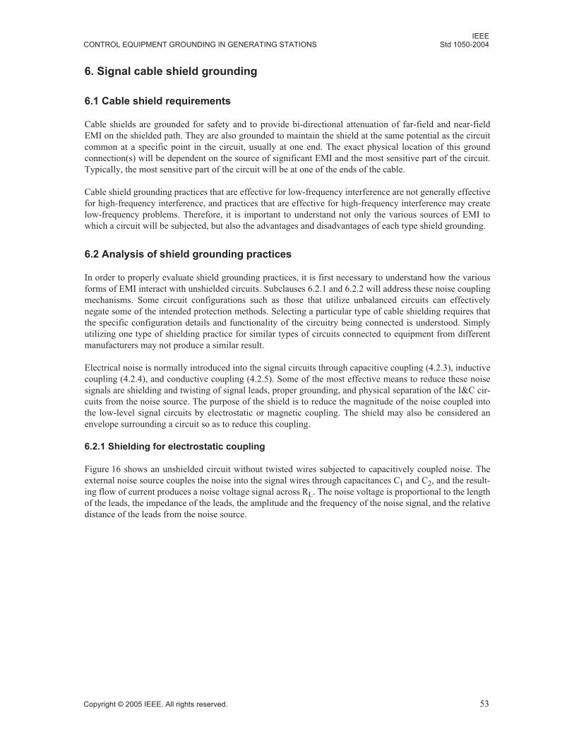
IEEECONTROL EQUIPMENT GROUNDING IN GENERATING STATIONS Std 1050-2004
6. Signal cable shield grounding
6.1 Cable shield requirements
Cable shields are grounded for safety and to provide bi-directional attenuation of far-field and near-fieldEMI on the shielded path. They are also grounded to maintain the shield at the same potential as the circuitcommon at a specific point in the circuit, usually at one end. The exact physical location of this groundconnection(s) will be dependent on the source of significant EMI and the most sensitive part of the circuit.Typically, the most sensitive part of the circuit will be at one of the ends of the cable.
Cable shield grounding practices that are effective for low-frequency interference are not generally effectivefor high-frequency interference, and practices that are effective for high-frequency interference may createlow-frequency problems. Therefore, it is important to understand not only the various sources of EMI towhich a circuit will be subjected, but also the advantages and disadvantages of each type shield grounding.
6.2 Analysis of shield grounding practices
In order to properly evaluate shield grounding practices, it is first necessary to understand how the variousforms of EMI interact with unshielded circuits. Subclauses 6.2.1 and 6.2.2 will address these noise couplingmechanisms. Some circuit configurations such as those that utilize unbalanced circuits can effectivelynegate some of the intended protection methods. Selecting a particular type of cable shielding requires thatthe specific configuration details and functionality of the circuitry being connected is understood. Simplyutilizing one type of shielding practice for similar types of circuits connected to equipment from differentmanufacturers may not produce a similar result.
Electrical noise is normally introduced into the signal circuits through capacitive coupling (4.2.3), inductivecoupling (4.2.4), and conductive coupling (4.2.5). Some of the most effective means to reduce these noisesignals are shielding and twisting of signal leads, proper grounding, and physical separation of the I&C cir-cuits from the noise source. The purpose of the shield is to reduce the magnitude of the noise coupled intothe low-level signal circuits by electrostatic or magnetic coupling. The shield may also be considered anenvelope surrounding a circuit so as to reduce this coupling.
6.2.1 Shielding for electrostatic coupling
Figure 16 shows an unshielded circuit without twisted wires subjected to capacitively coupled noise. Theexternal noise source couples the noise into the signal wires through capacitances C1 and C2, and the result-ing flow of current produces a noise voltage signal across RL. The noise voltage is proportional to the lengthof the leads, the impedance of the leads, the amplitude and the frequency of the noise signal, and the relativedistance of the leads from the noise source.
Copyright © 2005 IEEE. All rights reserved. 53
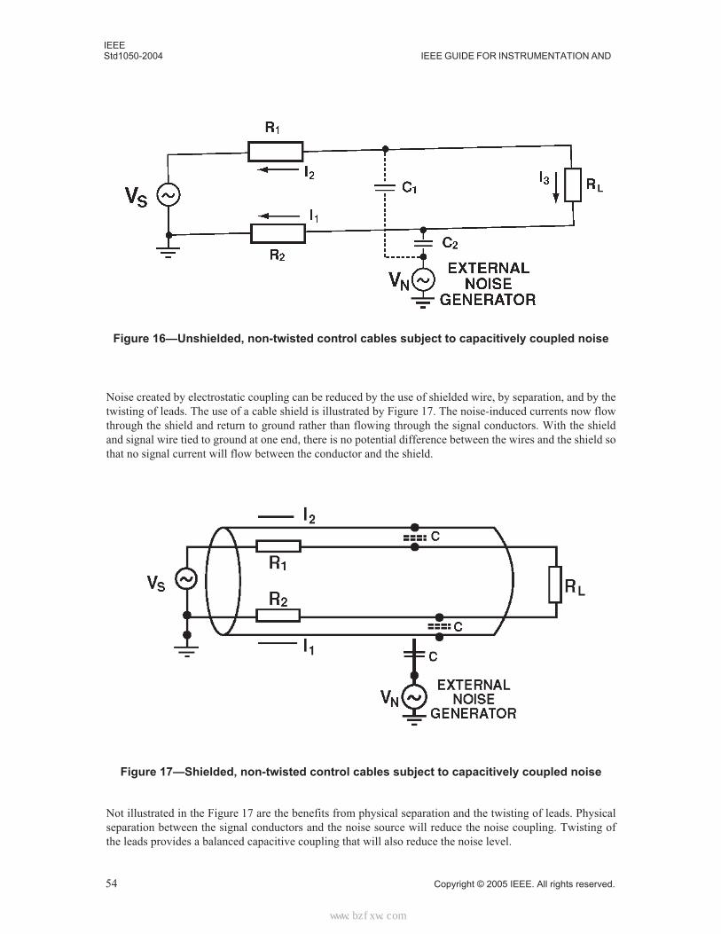
IEEEStd1050-2004 IEEE GUIDE FOR INSTRUMENTATION AND
Noise created by electrostatic coupling can be reduced by the use of shielded wire, by separation, and by thetwisting of leads. The use of a cable shield is illustrated by Figure 17. The noise-induced currents now flowthrough the shield and return to ground rather than flowing through the signal conductors. With the shieldand signal wire tied to ground at one end, there is no potential difference between the wires and the shield sothat no signal current will flow between the conductor and the shield.
Not illustrated in the Figure 17 are the benefits from physical separation and the twisting of leads. Physicalseparation between the signal conductors and the noise source will reduce the noise coupling. Twisting ofthe leads provides a balanced capacitive coupling that will also reduce the noise level.
Figure 16—Unshielded, non-twisted control cables subject to capacitively coupled noise
Figure 17—Shielded, non-twisted control cables subject to capacitively coupled noise
54 Copyright © 2005 IEEE. All rights reserved.
标准分享网 www.bzfxw.com 免费下载
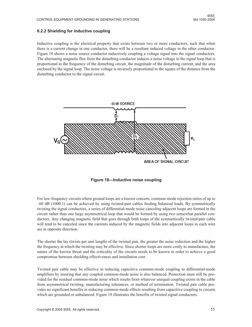
IEEECONTROL EQUIPMENT GROUNDING IN GENERATING STATIONS Std 1050-2004
6.2.2 Shielding for inductive coupling
Inductive coupling is the electrical property that exists between two or more conductors, such that whenthere is a current change in one conductor, there will be a resultant induced voltage in the other conductor.Figure 18 shows a noise source conductor inductively coupling a voltage signal into the signal conductors.The alternating magnetic flux from the disturbing conductor induces a noise voltage in the signal loop that isproportional to the frequency of the disturbing circuit, the magnitude of the disturbing current, and the areaenclosed by the signal loop. The noise voltage is inversely proportional to the square of the distance from thedisturbing conductor to the signal circuit.
For low-frequency circuits where ground loops are a known concern, common-mode rejection ratios of up to–60 dB (1000:1) can be achieved by using twisted-pair cables feeding balanced loads. By symmetricallytwisting the signal conductors, a series of differential-mode noise canceling adjacent loops are formed in thecircuit rather than one large asymmetrical loop that would be formed by using two somewhat parallel con-ductors. Any changing magnetic field that goes through both loops of the symmetrically twisted-pair cablewill tend to be canceled since the currents induced by the magnetic fields into adjacent loops in each wireare in opposite direction.
The shorter the lay (twists per unit length) of the twisted pair, the greater the noise reduction and the higherthe frequency at which the twisting may be effective. Since shorter loops are more costly to manufacture, thenature of the known threat and the criticality of the circuits needs to be known in order to achieve a goodcompromise between shielding effectiveness and installation cost.
Twisted pair cable may be effective in reducing capacitive common-mode coupling to differential-modeamplifiers by insuring that any coupled common-mode noise is also balanced. Protection must still be pro-vided for the residual common-mode noise which results from whatever unequal coupling exists in the cablefrom asymmetrical twisting, manufacturing tolerances, or method of termination. Twisted pair cable pro-vides no significant benefits in reducing common-mode effects resulting from capacitive coupling to circuitswhich are grounded or unbalanced. Figure 19 illustrates the benefits of twisted signal conductors.
Figure 18—Inductive noise coupling
Copyright © 2005 IEEE. All rights reserved. 55
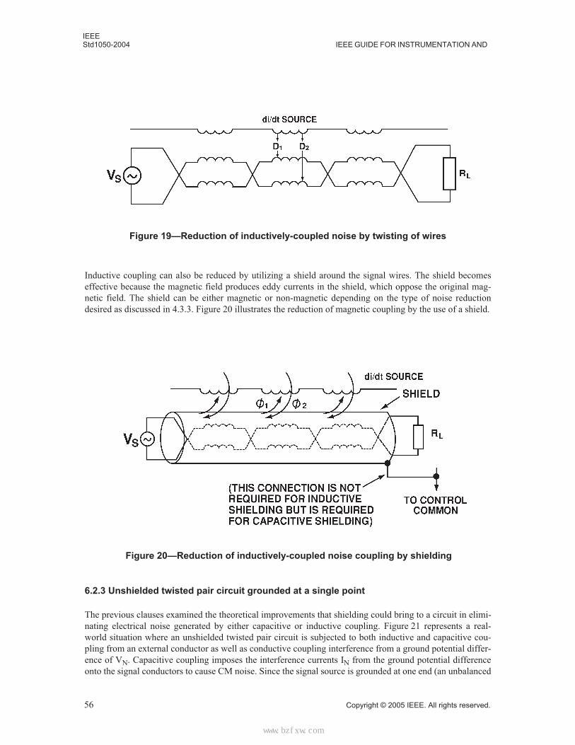
IEEEStd1050-2004 IEEE GUIDE FOR INSTRUMENTATION AND
Inductive coupling can also be reduced by utilizing a shield around the signal wires. The shield becomeseffective because the magnetic field produces eddy currents in the shield, which oppose the original mag-netic field. The shield can be either magnetic or non-magnetic depending on the type of noise reductiondesired as discussed in 4.3.3. Figure 20 illustrates the reduction of magnetic coupling by the use of a shield.
6.2.3 Unshielded twisted pair circuit grounded at a single point
The previous clauses examined the theoretical improvements that shielding could bring to a circuit in elimi-nating electrical noise generated by either capacitive or inductive coupling. Figure 21 represents a real-world situation where an unshielded twisted pair circuit is subjected to both inductive and capacitive cou-pling from an external conductor as well as conductive coupling interference from a ground potential differ-ence of VN. Capacitive coupling imposes the interference currents IN from the ground potential differenceonto the signal conductors to cause CM noise. Since the signal source is grounded at one end (an unbalanced
Figure 19—Reduction of inductively-coupled noise by twisting of wires
Figure 20—Reduction of inductively-coupled noise coupling by shielding
56 Copyright © 2005 IEEE. All rights reserved.
标准分享网 www.bzfxw.com 免费下载
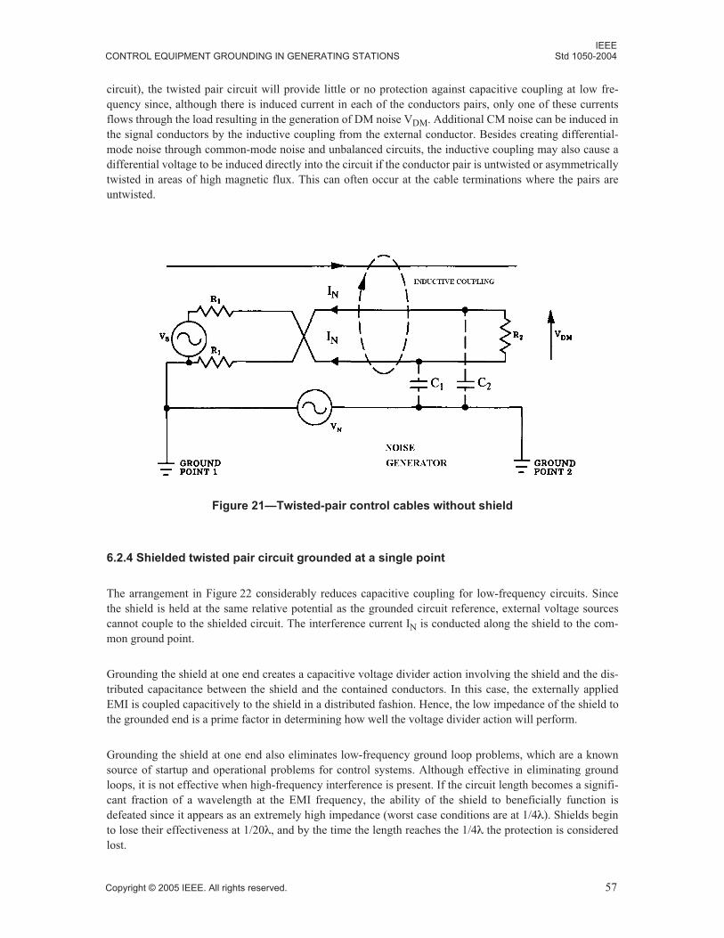
IEEECONTROL EQUIPMENT GROUNDING IN GENERATING STATIONS Std 1050-2004
circuit), the twisted pair circuit will provide little or no protection against capacitive coupling at low fre-quency since, although there is induced current in each of the conductors pairs, only one of these currentsflows through the load resulting in the generation of DM noise VDM. Additional CM noise can be induced inthe signal conductors by the inductive coupling from the external conductor. Besides creating differential-mode noise through common-mode noise and unbalanced circuits, the inductive coupling may also cause adifferential voltage to be induced directly into the circuit if the conductor pair is untwisted or asymmetricallytwisted in areas of high magnetic flux. This can often occur at the cable terminations where the pairs areuntwisted.
6.2.4 Shielded twisted pair circuit grounded at a single point
The arrangement in Figure 22 considerably reduces capacitive coupling for low-frequency circuits. Sincethe shield is held at the same relative potential as the grounded circuit reference, external voltage sourcescannot couple to the shielded circuit. The interference current IN is conducted along the shield to the com-mon ground point.
Grounding the shield at one end creates a capacitive voltage divider action involving the shield and the dis-tributed capacitance between the shield and the contained conductors. In this case, the externally appliedEMI is coupled capacitively to the shield in a distributed fashion. Hence, the low impedance of the shield tothe grounded end is a prime factor in determining how well the voltage divider action will perform.
Grounding the shield at one end also eliminates low-frequency ground loop problems, which are a knownsource of startup and operational problems for control systems. Although effective in eliminating groundloops, it is not effective when high-frequency interference is present. If the circuit length becomes a signifi-cant fraction of a wavelength at the EMI frequency, the ability of the shield to beneficially function isdefeated since it appears as an extremely high impedance (worst case conditions are at 1/4λ). Shields beginto lose their effectiveness at 1/20λ, and by the time the length reaches the 1/4λ the protection is consideredlost.
Figure 21—Twisted-pair control cables without shield
Copyright © 2005 IEEE. All rights reserved. 57
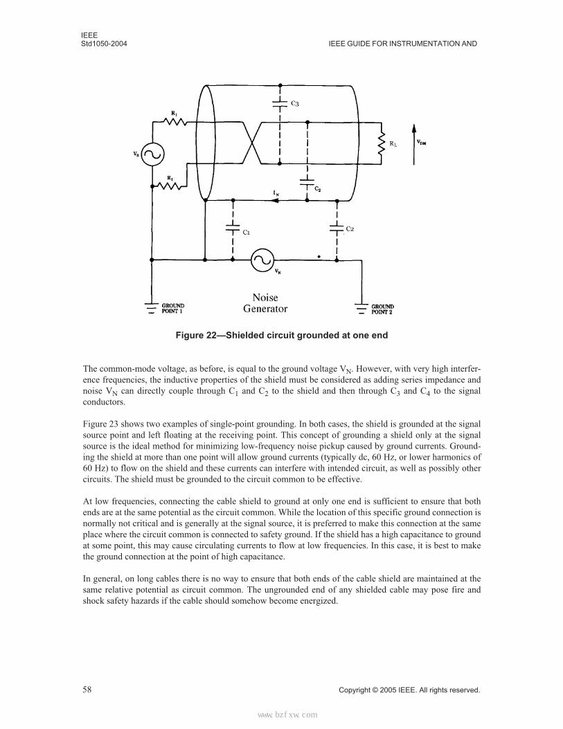
IEEEStd1050-2004 IEEE GUIDE FOR INSTRUMENTATION AND
The common-mode voltage, as before, is equal to the ground voltage VN. However, with very high interfer-ence frequencies, the inductive properties of the shield must be considered as adding series impedance andnoise VN can directly couple through C1 and C2 to the shield and then through C3 and C4 to the signalconductors.
Figure 23 shows two examples of single-point grounding. In both cases, the shield is grounded at the signalsource point and left floating at the receiving point. This concept of grounding a shield only at the signalsource is the ideal method for minimizing low-frequency noise pickup caused by ground currents. Ground-ing the shield at more than one point will allow ground currents (typically dc, 60 Hz, or lower harmonics of60 Hz) to flow on the shield and these currents can interfere with intended circuit, as well as possibly othercircuits. The shield must be grounded to the circuit common to be effective.
At low frequencies, connecting the cable shield to ground at only one end is sufficient to ensure that bothends are at the same potential as the circuit common. While the location of this specific ground connection isnormally not critical and is generally at the signal source, it is preferred to make this connection at the sameplace where the circuit common is connected to safety ground. If the shield has a high capacitance to groundat some point, this may cause circulating currents to flow at low frequencies. In this case, it is best to makethe ground connection at the point of high capacitance.
In general, on long cables there is no way to ensure that both ends of the cable shield are maintained at thesame relative potential as circuit common. The ungrounded end of any shielded cable may pose fire andshock safety hazards if the cable should somehow become energized.
Figure 22—Shielded circuit grounded at one end
58 Copyright © 2005 IEEE. All rights reserved.
标准分享网 www.bzfxw.com 免费下载
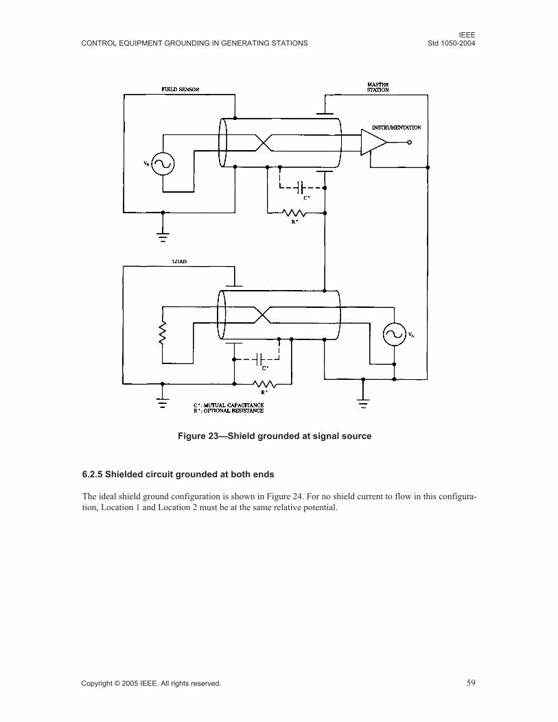
IEEECONTROL EQUIPMENT GROUNDING IN GENERATING STATIONS Std 1050-2004
6.2.5 Shielded circuit grounded at both ends
The ideal shield ground configuration is shown in Figure 24. For no shield current to flow in this configura-tion, Location 1 and Location 2 must be at the same relative potential.
Figure 23—Shield grounded at signal source
Copyright © 2005 IEEE. All rights reserved. 59
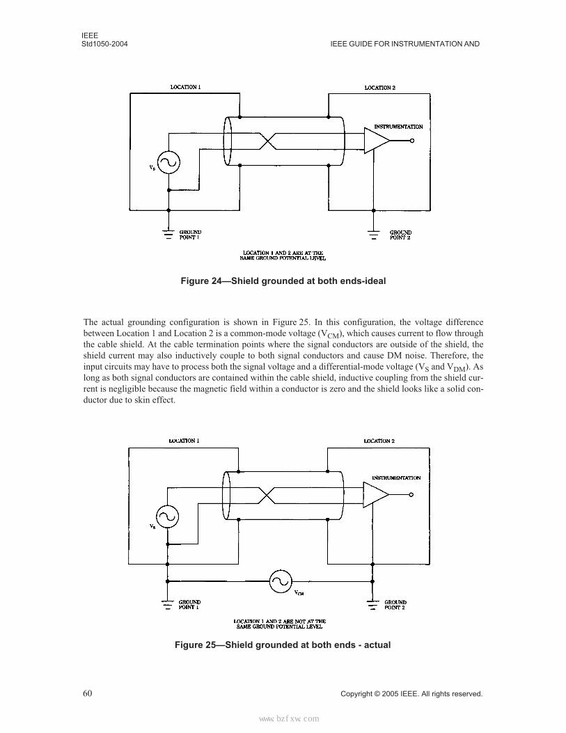
IEEEStd1050-2004 IEEE GUIDE FOR INSTRUMENTATION AND
The actual grounding configuration is shown in Figure 25. In this configuration, the voltage differencebetween Location 1 and Location 2 is a common-mode voltage (VCM), which causes current to flow throughthe cable shield. At the cable termination points where the signal conductors are outside of the shield, theshield current may also inductively couple to both signal conductors and cause DM noise. Therefore, theinput circuits may have to process both the signal voltage and a differential-mode voltage (VS and VDM). Aslong as both signal conductors are contained within the cable shield, inductive coupling from the shield cur-rent is negligible because the magnetic field within a conductor is zero and the shield looks like a solid con-ductor due to skin effect.
Figure 24—Shield grounded at both ends-ideal
Figure 25—Shield grounded at both ends - actual
60 Copyright © 2005 IEEE. All rights reserved.
标准分享网 www.bzfxw.com 免费下载
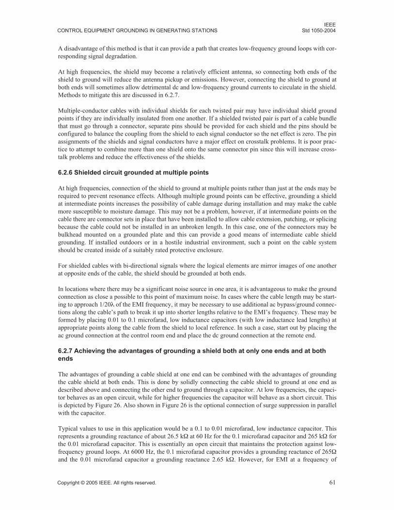
IEEECONTROL EQUIPMENT GROUNDING IN GENERATING STATIONS Std 1050-2004
A disadvantage of this method is that it can provide a path that creates low-frequency ground loops with cor-responding signal degradation.
At high frequencies, the shield may become a relatively efficient antenna, so connecting both ends of theshield to ground will reduce the antenna pickup or emissions. However, connecting the shield to ground atboth ends will sometimes allow detrimental dc and low-frequency ground currents to circulate in the shield.Methods to mitigate this are discussed in 6.2.7.
Multiple-conductor cables with individual shields for each twisted pair may have individual shield groundpoints if they are individually insulated from one another. If a shielded twisted pair is part of a cable bundlethat must go through a connector, separate pins should be provided for each shield and the pins should beconfigured to balance the coupling from the shield to each signal conductor so the net effect is zero. The pinassignments of the shields and signal conductors have a major effect on crosstalk problems. It is poor prac-tice to attempt to combine more than one shield onto the same connector pin since this will increase cross-talk problems and reduce the effectiveness of the shields.
6.2.6 Shielded circuit grounded at multiple points
At high frequencies, connection of the shield to ground at multiple points rather than just at the ends may berequired to prevent resonance effects. Although multiple ground points can be effective, grounding a shieldat intermediate points increases the possibility of cable damage during installation and may make the cablemore susceptible to moisture damage. This may not be a problem, however, if at intermediate points on thecable there are connector sets in place that have been installed to allow cable extension, patching, or splicingbecause the cable could not be installed in an unbroken length. In this case, one of the connectors may bebulkhead mounted on a grounded plate and this can provide a good means of intermediate cable shieldgrounding. If installed outdoors or in a hostile industrial environment, such a point on the cable systemshould be created inside of a suitably rated protective enclosure.
For shielded cables with bi-directional signals where the logical elements are mirror images of one anotherat opposite ends of the cable, the shield should be grounded at both ends.
In locations where there may be a significant noise source in one area, it is advantageous to make the groundconnection as close a possible to this point of maximum noise. In cases where the cable length may be start-ing to approach 1/20λ of the EMI frequency, it may be necessary to use additional ac bypass/ground connec-tions along the cable’s path to break it up into shorter lengths relative to the EMI’s frequency. These may beformed by placing 0.01 to 0.1 microfarad, low inductance capacitors (with low inductance lead lengths) atappropriate points along the cable from the shield to local reference. In such a case, start out by placing theac ground connection at the control room end and place the dc ground connection at the remote end.
6.2.7 Achieving the advantages of grounding a shield both at only one ends and at both ends
The advantages of grounding a cable shield at one end can be combined with the advantages of groundingthe cable shield at both ends. This is done by solidly connecting the cable shield to ground at one end asdescribed above and connecting the other end to ground through a capacitor. At low frequencies, the capaci-tor behaves as an open circuit, while for higher frequencies the capacitor will behave as a short circuit. Thisis depicted by Figure 26. Also shown in Figure 26 is the optional connection of surge suppression in parallelwith the capacitor.
Typical values to use in this application would be a 0.1 to 0.01 microfarad, low inductance capacitor. Thisrepresents a grounding reactance of about 26.5 kΩ at 60 Hz for the 0.1 microfarad capacitor and 265 kΩ forthe 0.01 microfarad capacitor. This is essentially an open circuit that maintains the protection against low-frequency ground loops. At 6000 Hz, the 0.1 microfarad capacitor provides a grounding reactance of 265Ωand the 0.01 microfarad capacitor a grounding reactance 2.65 kΩ. However, for EMI at a frequency of
Copyright © 2005 IEEE. All rights reserved. 61
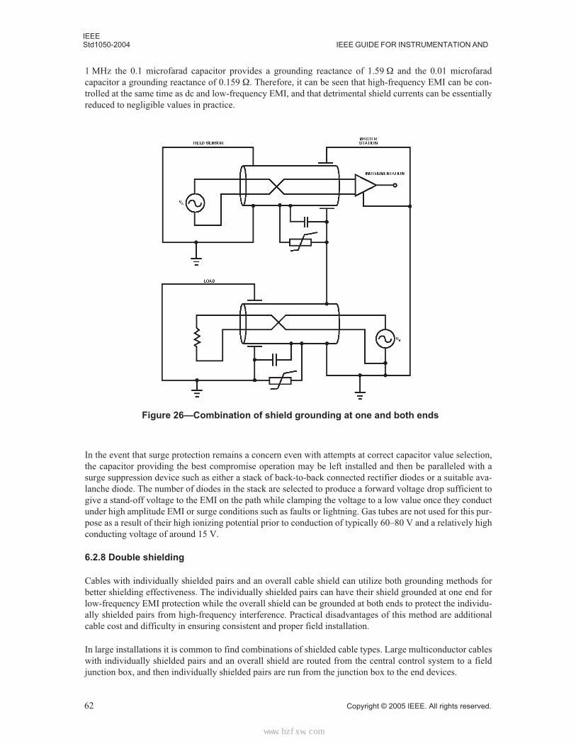
IEEEStd1050-2004 IEEE GUIDE FOR INSTRUMENTATION AND
1 MHz the 0.1 microfarad capacitor provides a grounding reactance of 1.59 Ω and the 0.01 microfaradcapacitor a grounding reactance of 0.159 Ω. Therefore, it can be seen that high-frequency EMI can be con-trolled at the same time as dc and low-frequency EMI, and that detrimental shield currents can be essentiallyreduced to negligible values in practice.
In the event that surge protection remains a concern even with attempts at correct capacitor value selection,the capacitor providing the best compromise operation may be left installed and then be paralleled with asurge suppression device such as either a stack of back-to-back connected rectifier diodes or a suitable ava-lanche diode. The number of diodes in the stack are selected to produce a forward voltage drop sufficient togive a stand-off voltage to the EMI on the path while clamping the voltage to a low value once they conductunder high amplitude EMI or surge conditions such as faults or lightning. Gas tubes are not used for this pur-pose as a result of their high ionizing potential prior to conduction of typically 60–80 V and a relatively highconducting voltage of around 15 V.
6.2.8 Double shielding
Cables with individually shielded pairs and an overall cable shield can utilize both grounding methods forbetter shielding effectiveness. The individually shielded pairs can have their shield grounded at one end forlow-frequency EMI protection while the overall shield can be grounded at both ends to protect the individu-ally shielded pairs from high-frequency interference. Practical disadvantages of this method are additionalcable cost and difficulty in ensuring consistent and proper field installation.
In large installations it is common to find combinations of shielded cable types. Large multiconductor cableswith individually shielded pairs and an overall shield are routed from the central control system to a fieldjunction box, and then individually shielded pairs are run from the junction box to the end devices.
Figure 26—Combination of shield grounding at one and both ends
62 Copyright © 2005 IEEE. All rights reserved.
标准分享网 www.bzfxw.com 免费下载
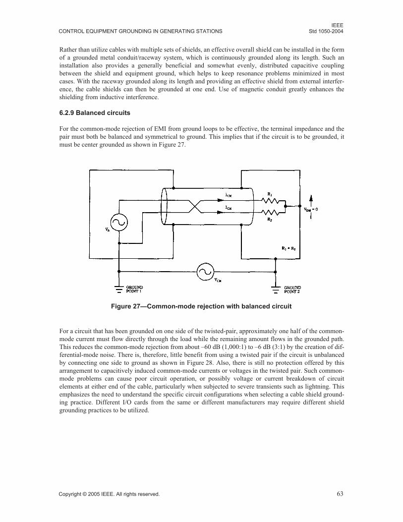
IEEECONTROL EQUIPMENT GROUNDING IN GENERATING STATIONS Std 1050-2004
Rather than utilize cables with multiple sets of shields, an effective overall shield can be installed in the formof a grounded metal conduit/raceway system, which is continuously grounded along its length. Such aninstallation also provides a generally beneficial and somewhat evenly, distributed capacitive couplingbetween the shield and equipment ground, which helps to keep resonance problems minimized in mostcases. With the raceway grounded along its length and providing an effective shield from external interfer-ence, the cable shields can then be grounded at one end. Use of magnetic conduit greatly enhances theshielding from inductive interference.
6.2.9 Balanced circuits
For the common-mode rejection of EMI from ground loops to be effective, the terminal impedance and thepair must both be balanced and symmetrical to ground. This implies that if the circuit is to be grounded, itmust be center grounded as shown in Figure 27.
For a circuit that has been grounded on one side of the twisted-pair, approximately one half of the common-mode current must flow directly through the load while the remaining amount flows in the grounded path.This reduces the common-mode rejection from about –60 dB (1,000:1) to –6 dB (3:1) by the creation of dif-ferential-mode noise. There is, therefore, little benefit from using a twisted pair if the circuit is unbalancedby connecting one side to ground as shown in Figure 28. Also, there is still no protection offered by thisarrangement to capacitively induced common-mode currents or voltages in the twisted pair. Such common-mode problems can cause poor circuit operation, or possibly voltage or current breakdown of circuitelements at either end of the cable, particularly when subjected to severe transients such as lightning. Thisemphasizes the need to understand the specific circuit configurations when selecting a cable shield ground-ing practice. Different I/O cards from the same or different manufacturers may require different shieldgrounding practices to be utilized.
Figure 27—Common-mode rejection with balanced circuit
Copyright © 2005 IEEE. All rights reserved. 63
IEEEStd1050-2004 IEEE GUIDE FOR INSTRUMENTATION AND
If balanced grounding is not a viable option, it may be better to galvanically float the receiver at its enclosureto increase the ground loop impedance and lower the common-mode current in the twisted pair, This action,however, replaces the galvanic connection with a stray or parasitic capacitance coupling mechanismbetween the enclosure and the “floated” item(s) inside of it. This can produce new problems that are worsethan the existing problem. Floating ground systems are generally not recommended as discussed in 5.2.3.
6.2.10 Coaxial cable
Coaxial cable can be used to transmit signals of all frequencies. It is particularly useful for signals above300 kHz. Upper limits on frequency are in the range of a few-hundred megahertz where cable losses appearto be the limiting factor. In this type of cable, the inner-surface of the outer conductor (shield) acts as one ofthe two conductors for the signal. It also provides an EMI path on its outer surface by taking advantage ofskin-effects to keep the signal and EMI current separate in the shield’s cross-section. Since the two signalconductors have the same axis (coaxial), the net magnetic flux created external to the cable by the signalprocess current is zero and likewise the net voltage induced in each conductor due to an external magneticfield is zero.
The particular frequency below which a shield will offer practically no useful attenuation is termed the cut-off frequency and is defined as:
fc = Rs / (2pLs) (5)
where: Rs = Shield resistance,
Ls = Self-inductance of the shield.
Cutoff frequencies for standard coaxial cables range from 0.5–10 kHz, and this range is directly related tothe length of the subject cable as well as its construction characteristics. For example, very short coaxialcable with heavy-wall copper shielding will operate at lower frequency than a longer one with thin-wallshielding.
Figure 28—Common-mode rejection nullified by ground
64 Copyright © 2005 IEEE. All rights reserved.
标准分享网 www.bzfxw.com 免费下载
IEEECONTROL EQUIPMENT GROUNDING IN GENERATING STATIONS Std 1050-2004
As the frequency increases above the cutoff frequency, the shield offers increasing attenuation. Theimprovement in shielding effectiveness results from the reduction in loop area caused by current returningon the shield rather than via the external ground plane established by the site’s grounding system, and not byany magnetic shielding properties of the shield itself. At higher frequencies, coaxial cable will begin to looklike triaxial cable when the skin depths on the inner and outer surface of the shield do not overlap and thesignal process current flows exclusively on the inner surface of the cable’s shield. This is the ideal point ofoperation for coaxial cable.
For coaxial shielding to be effective, the shield must be properly terminated and the center conductor mustbe kept in the center. The practice of twisting the braid of a coaxial cable and point soldering it to the base ofa connector or other termination point will cause currents that were flowing symmetrically on the coaxialouter conductor to become asymmetrical at this point and possibly couple to the signal conductor that waspreviously centered. This may result in a –20 dB (10:1) or more degradation in the effectiveness of theshield at high frequencies. These “pigtail” terminations also act as antennae and can both radiate and receiveEMI in the local area in which they are installed. Finally, such asymmetrical terminations of the cable’s endcause an impedance “bump” in the cable, which will cause reflections of the transmitted signal to occur onthe signal path with associated standing wave resonance problems, including possible dielectric failures onhigher power circuits. This impedance mismatch, therefore, degrades the signal process and may introducedata transfer errors. Accordingly, the braid should be soldered or connector terminated so that it completelyand symmetrically encloses the inner conductor at the connection junction and does so with minimumimpedance change.
Sharply bending a coaxial cable will displace the center conductor and also cause coupling from the outerconductor to the now displaced center conductor. The maximum possible bend radius should be used whenrouting coaxial cable. In general, the minimum bend radius should never be less than 10 times the nominaldiameter of the cable.
At lower frequencies, if the cable has multiple ground connections, the return current may travel externallybetween the cable’s ends via the site’s grounding system rather than through the shield. This unwantedaction creates magnetic fields in unknown areas outside the coaxial cable. In the vicinity of the coaxialcable, the signal and return currents are no longer equal and there is now a net magnetic flux created in thisarea also. A coaxial cable carrying low-frequency signals will not retain its immunity to external fields sinceany disturbance of the cable’s unbalanced fields will now concurrently disturb the contained signal processas well. Also, the circuit will have a second loop through the ground connection, which may have significantinduced voltage. Therefore, with low-frequency signals the non-ferrous metal shield of a multiple-groundedcoaxial cable offers practically no H-field shielding. This is particularly a problem with audio and videobaseband signal processes.
6.3 Other cable shielding considerations
a) Connecting the spare conductors in a cable to ground at both ends has been found to increase theshielding effectiveness of the cable by increasing the amount of grounded metal appearing as ashield, as well as reducing the EMI resulting from parasitic oscillations occurring in the manyradiating dipoles that these ungrounded conductors create as a result of the distributed stray LCproducts. This latter effect is important because of the close proximity of these conductors to theactive signal conductors in the same cable. Grounding the spare conductors at each end can alsoincrease low-frequency ground loop problems.
b) If the control cables are being laid in a cable trench, additional low-frequency magnetic shielding ofthe cables can be provided by running a 4/0 ground grid conductor either inside or on top of thetrench. Trenches represent known serious EMI and surge current coupling possibilities. This is gen-erally the result of two often interrelated effects: (1) use of non-metallic conduit or raceway and; (2)tight spacing between the victim and aggressor cables, which results from the need to keep thetrenching operation minimized. A known example of this unwanted situation is where a single
Copyright © 2005 IEEE. All rights reserved. 65
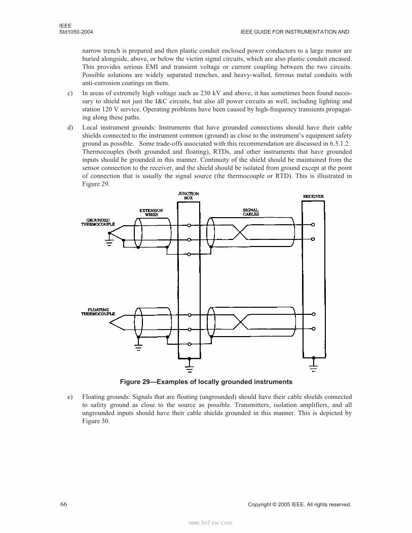
IEEEStd1050-2004 IEEE GUIDE FOR INSTRUMENTATION AND
narrow trench is prepared and then plastic conduit enclosed power conductors to a large motor areburied alongside, above, or below the victim signal circuits, which are also plastic conduit encased.This provides serious EMI and transient voltage or current coupling between the two circuits.Possible solutions are widely separated trenches, and heavy-walled, ferrous metal conduits withanti-corrosion coatings on them.
c) In areas of extremely high voltage such as 230 kV and above, it has sometimes been found neces-sary to shield not just the I&C circuits, but also all power circuits as well, including lighting andstation 120 V service. Operating problems have been caused by high-frequency transients propagat-ing along these paths.
d) Local instrument grounds: Instruments that have grounded connections should have their cableshields connected to the instrument common (ground) as close to the instrument’s equipment safetyground as possible. Some trade-offs associated with this recommendation are discussed in 6.5.1.2.Thermocouples (both grounded and floating), RTDs, and other instruments that have groundedinputs should be grounded in this manner. Continuity of the shield should be maintained from thesensor connection to the receiver, and the shield should be isolated from ground except at the pointof connection that is usually the signal source (the thermocouple or RTD). This is illustrated inFigure 29.
e) Floating grounds: Signals that are floating (ungrounded) should have their cable shields connectedto safety ground as close to the source as possible. Transmitters, isolation amplifiers, and allungrounded inputs should have their cable shields grounded in this manner. This is depicted byFigure 30.
Figure 29—Examples of locally grounded instruments
66 Copyright © 2005 IEEE. All rights reserved.
标准分享网 www.bzfxw.com 免费下载
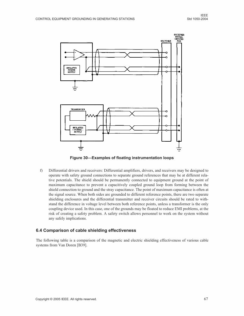
IEEECONTROL EQUIPMENT GROUNDING IN GENERATING STATIONS Std 1050-2004
f) Differential drivers and receivers: Differential amplifiers, drivers, and receivers may be designed tooperate with safety ground connections to separate ground references that may be at different rela-tive potentials. The shield should be permanently connected to equipment ground at the point ofmaximum capacitance to prevent a capacitively coupled ground loop from forming between theshield connection to ground and the stray capacitance. The point of maximum capacitance is often atthe signal source. When both sides are grounded to different reference points, there are two separateshielding enclosures and the differential transmitter and receiver circuits should be rated to with-stand the difference in voltage level between both reference points, unless a transformer is the onlycoupling device used. In this case, one of the grounds may be floated to reduce EMI problems, at therisk of creating a safety problem. A safety switch allows personnel to work on the system withoutany safely implications.
6.4 Comparison of cable shielding effectiveness
The following table is a comparison of the magnetic and electric shielding effectiveness of various cablesystems from Van Doren [B39].
Figure 30—Examples of floating instrumentation loops
Copyright © 2005 IEEE. All rights reserved. 67
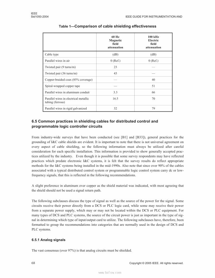
IEEEStd1050-2004 IEEE GUIDE FOR INSTRUMENTATION AND
6.5 Common practices in shielding cables for distributed control and programmable logic controller circuits
From industry-wide surveys that have been conducted (see [B1] and [B33]), general practices for thegrounding of I&C cable shields are evident. It is important to note that there is not universal agreement onevery aspect of cable shielding, so the following information must always be utilized after carefulconsideration for each specific installation. This information is provided to show generally accepted prac-tices utilized by the industry. Even though it is possible that some survey respondents may have reflectedpractices which predate electronic I&C systems, it is felt that the survey results do reflect appropriatemethods for the I&C systems being installed in the mid-1990s. Also note that since over 90% of the cablesassociated with a typical distributed control system or programmable logic control system carry dc or low-frequency signals, that this is reflected in the following recommendations.
A slight preference in aluminum over copper as the shield material was indicated, with most agreeing thatthe shield should not be used a signal return path.
The following subclauses discuss the type of signal as well as the source of the power for the signal. Somecircuits receive their power directly from a DCS or PLC logic card, while some may receive their powerfrom a separate power supply, which may or may not be located within the DCS or PLC equipment. Formany types of DCS and PLC systems, the source of the circuit power is just as important in the type of sig-nal in determining which type of input/output card to utilize. The following subclauses have, therefore, beenformatted to group the recommendations into categories that are normally used in the design of DCS andPLC systems.
6.5.1 Analog signals
The vast consensus (over 97%) is that analog circuits must be shielded.
Table 1—Comparison of cable shielding effectiveness
60 HzMagnetic
fieldattenuation
100 kHzElectric
fieldattenuation
Cable type (dB) (dB)
Parallel wires in air 0 (Ref.) 0 (Ref.)
Twisted pair (9 turns/m) 23 —
Twisted pair (36 turns/m) 43 —
Copper-braided coax (85% coverage) — 40
Spiral-wrapped copper tape — 51
Parallel wires in aluminum conduit 3.3 66
Parallel wires in electrical metallic tubing (ferrous)
16.5 70
Parallel wires in rigid galvanized 32 79
68 Copyright © 2005 IEEE. All rights reserved.
标准分享网 www.bzfxw.com 免费下载
IEEECONTROL EQUIPMENT GROUNDING IN GENERATING STATIONS Std 1050-2004
6.5.1.1 Analog inputs powered by a DCS or PLC
For this type of circuit, 46% of industry respondents utilize individually shielded pairs only, 12% utilize anoverall shield only, and 39% utilize cables that have individually shielded pairs plus and overall cable shield.No cable shield was recommended by 3% of the respondents. The shield should be grounded at the DCS orPLC according to 90% of the respondents, while 10% would ground the shield at the field device.
6.5.1.2 Analog inputs powered by an external source
For this type of circuit, 46% of industry respondents utilize individually shielded pairs only, 12% utilize anoverall shield only, and 39% utilize cables which have individually shielded pairs plus an overall cableshield. No cable shield was recommended by 3% of the respondents. The shield should be grounded at theDCS or PLC according to 79% of the respondents, while 21% would ground the shield at the field device.Compared to the previous item, the difference in where the shield is grounded reflects that a slightly higherpercentage are grounding the shield at the field device since this is generally the best location according totheory. That the percentage acting according to ideal theory is not that large appears to reflect the practicaldifficulties encountered during installation and checkout if cable shields are grounded at different locationson a circuit-by-circuit basis. There are practical advantages for grounding all cable shields at one point, withexperience showing that the few circuits that experience difficulties because of a uniform approach can becorrected during startup or early operation.
6.5.1.3 Analog voltage and current transformer inputs
The magnitudes of these signals are generally not directly compatible with the input ratings of DCS or PLCinputs and must be processed with a transducer. These would follow the same recommendations for otheranalog input signals, depending on whether the transducer is loop-powered or provided with an externalpower supply.
6.5.1.4 Analog outputs powered by a DCS or PLC
For this type of circuit, all of the respondents recommended utilizing shielded cables, with 45% utilizingindividually shielded pairs only, 16%, utilizing an overall shield only, and 39% utilizing cables that haveindividually shielded pairs plus and overall cable shield. The shield should be grounded at the DCS or PLCaccording to 90% of the respondents, while 10% would ground the shield at the field device.
6.5.2 Digital (dry contact change of state) signals
Digital (discrete) information in this context refers to the monitoring of a contact change of state, which istypically done with a dc voltage. This should not be confused with high-frequency “digital” communicationscircuits, which are discussed in 6.5.3. The shielding recommendations for these two types of “digital” cir-cuits are completely different, and the similar nomenclature has undoubtedly caused some confusion in theproper application of cable shield grounding practices.
The survey results show that approximately one-half of the respondents feel that there is no need for theshielding of these circuits. Since these circuits have a high signal-to-noise ratio it was expected that the per-centage of respondents not shielding these circuits would be higher. Two items may account for the receivedresponse. The first is that the survey did not specifically differentiate the wetting voltage. Respondents whoutilize a relatively low-voltage level such as 24 Vdc may feel that shielding is required. The second reason isthat it is the practice of some utilities to utilize shielded cable for all DCS and PLC circuits as part of theirstandard practice since it has the practical benefits of materials standardization and ensures that installationcrews recognize the special nature of these circuits. Some of these same utilities also have the practice of notterminating the shields at either end for digital input and output circuits since the circuit susceptibility is lowand shielding is not required. One utility has even standardized on separate colored cable for digital inputs,digital outputs, analog inputs, and analog outputs. That way a quick glance can tell whether the circuit has
Copyright © 2005 IEEE. All rights reserved. 69
IEEEStd1050-2004 IEEE GUIDE FOR INSTRUMENTATION AND
been landed on the appropriate DCS or PLC input/output card. The advantages of this method come with thedisadvantages related to consistency of application, material procurement, and warehouse costs.
6.5.2.1 Digital inputs wetted by the DCS or PLC
For this type of circuit, 43% of industry respondents felt that no shielding was required, 29% utilize individ-ually shielded pairs only, 14% utilize an overall shield only, and 14% utilize cables that have individuallyshielded pairs plus an overall cable shield. The shield should be grounded at the DCS or PLC according to86% of the respondents, while 14% would ground the shield at the field device.
6.5.2.2 Digital inputs wetted by an external device
For this type of circuit, 58% of industry respondents felt that no shielding was required, 18% utilize individ-ually shielded pairs only, 12% utilize an overall shield only, and 12% utilize cables that have individuallyshielded pairs plus and overall cable shield. The shield should be grounded at the DCS or PLC according to83% of the respondents, while 17% would ground the shield at the field device.
6.5.2.3 Digital outputs wetted by the DCS or PLC
For this type of circuit, 56% of industry respondents felt that no shielding was required, 20% utilize individ-ually shielded pairs only, 12% utilize an overall shield only, and 12% utilize cables that have individuallyshielded pairs plus and overall cable shield. The shield should be grounded at the DCS or PLC according to88% of the respondents, while 12% would ground the shield at the field device.
6.5.2.4 Digital outputs wetted by an external device
For this type of circuit, 59% of industry respondents felt that no shielding was required, 17% utilize individ-ually shielded pairs only, 12% utilize an overall shield only, and 12% utilize cables that have individuallyshielded pairs plus and overall cable shield. The shield should be grounded at the DCS or PLC according to88% of the respondents, while 12% would ground the shield at the field device.
6.5.3 Data highway/digital communication
For these circuits, it is recommended to follow the recommendations of the equipment vendor since eachvendor has specific requirements regarding installation methods, cable types, and allowable circuit lengths.Depending on the specific installation, these circuits are typically either shielded twisted pairs, coaxial, orfiber-optic cable.
6.6 Central distribution frame (CDF) grounding practice
In order to minimize the impact of low-frequency EMI on I&C cables, the ideal practice is to ground allcable shields only at the signal source. This would, however, result in a widely distributed grounding systemwith the following disadvantages.
a) Increased difficulty of controlling shield grounding practices through both the design and construc-tion phases, with experience indicating the likely introduction of numerous ground loops.
b) Substantial increase in commissioning time as a result of locating and remediating ground loopproblems.
This CDF grounding approach creates a central grounded reference at, or close to, the plant control room.Combined with other practices of minimizing noise generation in a generating station, this system has beenproven to provide protection that minimizes noise coupling to acceptable levels. More sensitive signal andprocessing systems can be treated separately with the shield grounded at the source end.
70 Copyright © 2005 IEEE. All rights reserved.
标准分享网 www.bzfxw.com 免费下载
IEEECONTROL EQUIPMENT GROUNDING IN GENERATING STATIONS Std 1050-2004
The CDF provides an ideal system to permit the termination of trunk cabling systems. It reduces the quantityand length of ground conductors when compared to other grounding practices. These advantages haveresulted in substantial cost and schedule advantages in the construction of some commercial nuclear generat-ing stations. It has not been employed in a greenfield generating station design utilizing a modern micropro-cessor-based distributed control system.
The CDF grounding method is illustrated by Figure C.13.
6.6.1 Principles of CDF grounding
A single large insulated ground conductor is brought directly from the station ground mat (separate from thebuilding distributed ground system) to an insulated copper bus (typical cross section 25 mm × 6 mm) pro-vided on the CDF. This would normally be in a control equipment room immediately adjacent to the maincontrol center.
This bus would form the center of the signal ground and safety ground system for all field signals terminatedin the local area and not grounded elsewhere, such as signals connected to the computer or sensitive signalsgrounded at the other end. Within each CDF area, the signal and equipment grounds may be kept separate upto the point where they should exit the area. Then they are connected together and to the ground matconnection.
An alternative ground bus could be created by applying sheet metal to the wall in the form of a ground-planeand to bring all cables to this point for shield grounding and surge suppression connections. The groundplane is then low-inductance grounded/bonded to the equipment grounding system in the same area; thus,minimizing potential difference between the two. The advantage of this type of ground plane is that it avoidsthe unintentionally high level of inductance that can result from the CDF cabling method. The cable imped-ance is not related to cross-sectional area as much as it is surface area, and a ground-plane has a better geom-etry to take advantage of this fact.
6.6.2 Auxiliary computer CDF grounding
It may be expedient to provide a separate but similar ground bus at the main computer for all field signalsdirectly connected to the computer. This bus would be connected radially by an insulated ground cable fromthe primary CDF ground bus. This computer CDF would also serve as the central point from which each ofthe computer cabinet signal ground racks would be referenced.
7. Testing
7.1 General
This clause addresses testing to detect conductive ground loops on I&C circuits that may purposely or inad-vertently use the ground system as part of the signal return path. Ground loops are discussed in 4.2.2, 4.3.3,5.2.2, and 6.2. This clause does not address testing on those high-frequency systems where multiple-pointgrounding may be used, nor is it intended to be used to test ground systems that are not used for signalreturns. Finally, the testing described herein is not full-range testing since it does not account for capaci-tively or inductively coupled ground loops that respond to changing voltages and currents.
In addition to the above, it must be understood that there are three classes of ground loop: (1) harmful orunwanted, and; (2) benign, in that they appear to have no effects, and; (3) beneficial ground loops such asthose that carry surge currents, ac system fault currents, and prevent fires and shocks from occurring. Beforeembarking on any program to remove or otherwise eliminate any perceived ground loop, it is important toknow which of the three types it is, and what will be the total range of effects if it is removed, not just a sin-
Copyright © 2005 IEEE. All rights reserved. 71
IEEEStd1050-2004 IEEE GUIDE FOR INSTRUMENTATION AND
gular effect. A gain in noise reduction may result in the creation of a safety hazard under certain transientconditions
7.2 Sources of galvanic (conductive) ground loops
The primary sources of conductive ground loops are:
a) More than one ground erroneously placed at different points on a cable shield or signal return.
b) Shield and associated signal wires connected to ground at different locations. A ground loop will beformed through the ground points and the signal wire to shield capacitance.
c) Leakage paths caused by insulation failure, moisture, etc. Leakage paths from moisture normallyoccur at circuit devices, terminal strips, or connectors.
7.3 Galvanic ground loop prevention and detection
Ground loops are formed whenever two or more connections are made from different points in the circuit tothe station ground system. Current flow between the ground points may occur from potential differencesbetween the ground points, but even connections to the same ground point from different points in the circuitcan create large loops that will be sensitive to inductive coupling.
Different points on the station grounding system may be at different voltages as a result of current flowthrough the grounding system. The currents may be the result of power system transients, lightning, or anyof the sources listed in 4.1. As a result of these voltage differences in the station grounding system, conduc-tive ground loops may provide a path for current flow through the I&C cable conductors and/or shield viathe multiple ground points. This current flow may create CM noise on the signal circuit, and if strongenough, may cause failure of the circuit. It may also cause noise problems if the CM noise is converted tonormal mode noise by the circuits and terminations.
The currents of interest in galvanic ground loop problems are most commonly 60 Hz or a harmonic of60 Hz, with the third harmonic having been historically typical. This has been changing with higher orderharmonics causing problems due to the proliferation of non-linear loads that generate higher orders ofharmonic energy during their operation. Examples of this are phase-shift fired SCR loads and pulse-width-modulated driven equipment such as variable speed motor drivers.
The loop areas formed by connecting different points in the circuit to the same ground point will be sensitiveto current surges flowing in any of the associated grounding wires running to the same grounding point andcommonly bundled together.
To avoid ground loops in the initial installation, tests should be conducted to verify that ground loops do notexist. This may be accomplished as follows:
a) Where practical, before grounding shields, signal wires, etc., first make a crude go-no go check forisolation from ground using an ohmmeter. If no unintentional ground points are located, next usesome other calibrated device specifically capable of measuring insulation integrity. The resistancebetween the wire or shield and station ground should be greater than 1 megohm. The substitution ofsignal generator for the insulation tester will indicate how much of a ground-loop exists as a func-tion of frequency. This can provide a good indication of the importance of non-conductive paths.
b) Where low resistance indicates an improper ground, defective cabling, moisture, etc., the deficiencyshould be corrected. Only after the deficiency is corrected should the circuit, shield, etc., be con-nected to ground.
c) After all the equipment and instrument grounds are installed, the overall signal ground systemshould be checked as described in 7.4.
72 Copyright © 2005 IEEE. All rights reserved.
标准分享网 www.bzfxw.com 免费下载
IEEECONTROL EQUIPMENT GROUNDING IN GENERATING STATIONS Std 1050-2004
The above test will detect most conductive ground loops, except those formed when long cable shields andthe associated I&C circuits are grounded at different locations. The capacitance between these kinds oflengthy shield and the signal wires will permit dc charging current from an ohmmeter and test frequency acfor insulation testers to flow through the cable to ground capacitance. This creates test problems that must beguarded against so that the results are not misinterpreted. The best way to avoid loops formed in this manneris careful design, construction, and field verification of the installation along with the use of experiencedcable test personnel.
7.4 Testing for ground loops
Safety considerations.
It is not recommended practice to disconnect the sole equipment grounding conductor or to rely on a ques-tionable equipment ground via a circuitous route during testing when power is still applied to the equipment.For example, in a properly grounded metal conduit containing an equipment grounding conductor, there isnot a significant hazard in disconnecting the equipment ground wire or the conduit for testing, but not bothat the same. Any disconnecting of grounding connections for the purposes of testing must be done with anunderstanding of the safety implications of removing a particular connection.
Ground loops formed by multiple direct, inductive (via a choke), or resistive ground connections to the sta-tion ground grid can be detected by the procedure described below and illustrated in Figure 31. It will notdetect ground loops resulting from incorrect shield grounding as described in 7.2.
Copyright © 2005 IEEE. All rights reserved. 73
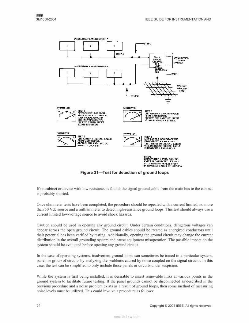
IEEEStd1050-2004 IEEE GUIDE FOR INSTRUMENTATION AND
If no cabinet or device with low resistance is found, the signal ground cable from the main bus to the cabinetis probably shorted.
Once ohmmeter tests have been completed, the procedure should be repeated with a current limited, no morethan 50 Vdc source and a milliammeter to detect high-resistance ground loops. This test should always use acurrent limited low-voltage source to avoid shock hazards.
Caution should be used in opening any ground circuit. Under certain conditions, dangerous voltages canappear across the open ground circuit. The ground cables should be treated as energized conductors untiltheir potential has been verified by testing. Additionally, opening the ground circuit may change the currentdistribution in the overall grounding system and cause equipment misoperation. The possible impact on thesystem should be evaluated before opening any ground circuit.
In the case of operating systems, inadvertent ground loops can sometimes be traced to a particular system,panel, or group of circuits by analyzing the problems caused by noise coupled on the signal circuits. In thiscase, the test can be simplified to only include those panels or circuits under suspicion.
While the system is first being installed, it is desirable to insert removable links at various points in theground system to facilitate future testing. If the panel grounds cannot be disconnected as described in theprevious procedure and a noise problem exists as a result of ground loops, then some method of measuringnoise levels must be utilized. This could involve a procedure as follows:
Figure 31—Test for detection of ground loops
74 Copyright © 2005 IEEE. All rights reserved.
标准分享网 www.bzfxw.com 免费下载
IEEECONTROL EQUIPMENT GROUNDING IN GENERATING STATIONS Std 1050-2004
a) Measure noise current/voltage on I&C ground cables connecting the main signal ground bus to thestation grounding system.
b) Measure noise current/voltage on cables connecting panels to the main signal ground bus.
c) Cables with noise current/voltage much higher than other cables may be shorted to ground.
d) Check the noise level on each cable connecting the panel to the faulted ground cable. Panel groundswith high noise levels should be checked.
e) Check the panel thoroughly and correct any inadvertent grounds.
This test is more effective if noise levels at various points are periodically monitored and recorded for futurereference. When a problem occurs, the noise levels can then be compared with previously recorded values.However, note that it is normal for some current to flow in a ground system due to capacitive couplingbetween energized circuit conductors, ground conductors, and cable shields. Thus, the presence of voltage orcurrent on an I&C ground cable does not necessarily mean a problem exists. Additionally, the absence ofnoise or no incorrect operation of circuits does not indicate the absence of ground loops or potential prob-lems. Problems caused by intermittent noise sources, such as lightning transients and power system groundfaults would be virtually impossible to locate during testing since the ground loops would only create aproblem when a transient or power system ground fault occurred. Thus, noise measurement tests may notnecessarily always be effective in locating unwanted ground loops and potential noise problems.
Noise measurements may, however, be useful in pointing to the cause. The frequency of the major noisecomponents will point to the noise source. The presence of 60 Hz and its principle harmonics would indicatethe power ground system as the source. For example, the presence of 180 Hz (the third harmonic of 60 Hz)would indicate a polyphase full-wave rectifier power supply as the probable source. Any relatively continu-ous high-frequency noise on a data system may be generated by corona discharge, phase-shift fired SCRs,and PWM controlled variable speed motor drives, or within the data system.
7.5 Signal ground system integrity
After initial installation, the following continuity/resistance measurements should be made:
a) Measure and log the resistance between the main signal ground bus and the station groundingsystem.
b) Measure and log the resistance between each cabinet signal ground point and the main instrumentground bus.
c) Compare the resistances to calculated or specified design goal values. If the resistances are high,check connections and correct any problems found. If resistance remains high, install larger groundcable, if required. Keeping ground conductors as short as possible is always advisable to minimizeground circuit impedance and thus limit noise voltage levels.
7.6 Maintenance of the signal ground system
Periodic inspections should be made of bolted connections to major signal ground buses. This check shouldinclude a visual inspection of all connections. Connections should be inspected for tightness and corrosion.
Copyright © 2005 IEEE. All rights reserved. 75
IEEEStd1050-2004 IEEE GUIDE FOR INSTRUMENTATION AND
Annex A
(informative)
Bibliography
[B1] “A Review of Manufacturer’s Recommendations for the Grounding of Distributed Control Systems inGenerating Stations,” IEEE Committee Report, IEEE Transactions on Energy Conversion, vol. 8, no. 1,March 1993.
[B2] Anders, R. and Campling, A. C., “Investigations into Interface in Substation and Power Station Auxil-iary Cabling,” CIGRE paper 36-09, 1976. Paper presented in the name of committee no 36, Interference.
[B3] ASEA Interference Handbook, Information Publication 7102001E, edition 2, 1981, Industrial Electron-ics Division, ASEA, S-721 83 Vasteras, Sweden.
[B4] Boersma, R., “Transient Ground Potential Rises in Gas Insulated Substations with Respect to EarthingSystems,” Presented at the Request of the Chairman of the CIGRE Study Committee 23, Electra no 110, pp.47–54.
[B5] Buckingham, R. P. and Gooding, F. H., “The Efficiency of Nonmagnetic Shields on Control and Com-munication Cable,” IEEE paper 69 TP 710-PWR.. Presented at the IEEE Summer Power Meeting 1969; vol.T-PAS 70, July/Aug 1970, pp. 1091-1099.
[B6] Cushing, V. J., Jr., “Transient Suppression in 500 kV Installations,” IEEE paper C 74 030-3. Presentedat the IEEE Power Engineering Society Winter Meeting, 1974, vol. T-PAS 74, July/Aug 1974, p. 1018.
[B7] Denny, H., Grounding for the Control of EMI, Gainesville, VA, Don White Consultants, Inc, 1983.
[B8] Denny, H. W., “Grounding in the Design of Building & Facilities for Safety Protection,” EMC Tech-nology, Jan-Mar 1983, pp. 22-34.
[B9] Dick, E. P., Fujimoto, N., Ford, G. L., and Harvey, S., “Transient Ground Potential Rise in Gas Insu-lated Switchgear-Problem Identification and Mitigation,” (82WM176-6); vol. T-PAS, Oct 1982, pp. 3610-3619.
[B10] Dietrich, R. E., Ramberg, H. C., and Barber, J. C., “BPA Experience with EMI Measurement andShielding,” Proceedings of the American Power Conference, vol. 32, 1970, pp. 1054-1061.
[B11] Electric Power Research Institute, Transmission Line Reference Book—345 kV and Above, secondedition, Palo Alto, CA, 1982, EL-2500.
[B12] Emery, F. F. and Harrold, R. T., “On Line Incipient Arc Detection in Large Turbine Generator StatorWindings,” IEEE Transactions on Power Apparatus and Systems, vol. PAS-99, no 6, Nov/Dec 1980, pp.2232-2238.
[B13] EMI Shielding Design Guide, Tecknit EMI Shielding Products, New York, 1982.
[B14] EPRI TR 102323, Rev. 2, “ Guidelines for Electromagnetic Interference Testing in Power Plants.”
[B15] EPRI TR-102400, Volumes 1 and 2, Handbook for Electromagnetic Compatibility for Digital Equip-ment in Power Plants. October 1994.
76 Copyright © 2005 IEEE. All rights reserved.
标准分享网 www.bzfxw.com 免费下载
IEEECONTROL EQUIPMENT GROUNDING IN GENERATING STATIONS Std 1050-2004
[B16] Fillenberg, R. R., Cleveland, G. W., and Harris, R. E., “Exploration of Transients by SwitchingCapacitors,” IEEE paper 70 TP 42-PWR presented at the IEEE Winter Power Meeting 1970, vol. T-PAS 71,Jan/Feb, pp. 250-260.
[B17] Gillies, D. A. and Ramberg, H. C., “Methods for Reducing Induced Voltages in Secondary Circuits,”IEEE paper 31 TP 66-329 presented at the IEEE Summer Power Meeting 1966, vol. T-PAS 67 63, supple-ment pp. 258-279.
[B18] Guidelines on Electrical Power for ADP Installation, Federal Information Processing Standards Pub-lication 94, Sep 1983.
[B19] Hayt, W. H., Jr., Engineering Electromagnetics, fourth edition, McGraw-Hill, Inc, New York, 1981,pp. 381-384.
[B20] Hicks, R. L. and Jones, D. E., “Transient Voltages on Power Station Wiring,” IEEE Transaction onPower Apparatus & Systems, vol. PAS-90, no 1, Jan/Feb 1971.
[B21] IEEE 100, The Authoritative Dictionary of IEEE Standard Terms.
[B22] IEEE Transactions on Aerospace and Electronic Applications, AES12, vol. 2, Mar 1976, p 104.
[B23] IEEE Working Group On Power System Harmonics, “Power System Harmonics: An Overview,” 85WM 139-3, presented at IEEE/PES 1983 Winter Meeting.
[B24] Jancauskas, J. R., Grant, L. A. D. G. and Thaden, M. V., “Use of Single Point Grounding for Instru-mentation and Control Systems Installed in Existing Generating Stations,” IEEE Transaction on EnergyConversion, Vol. 4, No. 3, September 1989, pages 402-405.
[B25] Klipec, B. E., “Reducing Electrical Noise in Instrument Circuits,” IEEE Transactions on Industry andGeneral Applications, vol. IGA-3, no 2, Mar/Apr 1967.
[B26] Kotheimer, W. C., “Influence of Station Design on Control Circuit Transients,” Proceedings of theAmerican Power Conference, 1969, pp. 1021-1028.
[B27] Kotheimer, W. C., “Radiated EMI Susceptibility of Electric Utility Control Devices and Systems,” apaper presented at the Edison Electric Institute meeting held in Springfield, IL, Oct 12 and 13, 1987.
[B28] Kotheimer, W. C., “Theory of Shielding & Grounding of Control Cables to Reduce Surges,” a paperpresented at the Fall Meeting of Pennsylvania Electric Association, Oct 5, 1973.
[B29] Martin, L. C., “Transorb & Metal Oxide Varistor Comparison,” Lawrence Livermore LaboratoryPublication, PEM-53.
[B30] Martin, R. E., Electrical Interference in Electronic Systems, Forest Grove or Research Studies Press.
[B31] Michael, D. T., “Proposed Design Standard for the Voltage Drop in Building Wiring for Low-VoltageSystems,” IEEE Transactions on Industry and General Applications, vol. IGA-4, Jan/Feb 1968, pp. 30-32.
[B32] Morrison, R., Grounding and Shielding Techniques in Instrumentation, third edition, Long Beach,CA, John Wiley and Sons, 1977.
[B33] Panel Session on “Grounding Requirements for Distributed Control Systems,” IEEE Power Engi-neerign Society, 1999 Summer Meeting.
Copyright © 2005 IEEE. All rights reserved. 77
IEEEStd1050-2004 IEEE GUIDE FOR INSTRUMENTATION AND
[B34] Seibert, G. C., EPRI Power Plant Electrical Reference Series, vol. 14, Electrical Noise Reduction,prepared by Stone and Webster.
[B35] Summary of the Guide for the Grounding of Instrument Transformer Secondary Circuits and Cases,(87SM627-3), July 1987.
[B36] Turesin, V. M., “Electromagnetic Compatibility Guide for Design Engineers,” IEEE Transactions onEMC, vol. EMC-9, no 3, Dec 1967, pp. 139-145.
[B37] United States Atomic Energy Commission. Division of Reactor Development and Technology RDTC1-1T, Standard on Instrumentation and Control Equipment Grounding and Shielding Practices, Jan 1973.
[B38] USNRC Regulatory Guide 1.180, “Guidelines for Evaluating Electromagnetic and Radio-FrequencyInterference in Safety-Related Instrumentation and Control Systems,” January 2000.
[B39] Van Doren, T. P., “Grounding & Shielding Electronic Instrumentation,” University of Missouri-Rolla1985. Seminar presented May 6, 1985 in Silver Springs, MD.
[B40] Weed, J.E., and H.G. Hudson, D. M. Wythe, E. J. Bogdan, “Investigation of Electromagnetic Interfer-ence (EMI) Levels in Commercial Nuclear Power Plants,” NUREG/CR 3270 UCID-19703.
[B41] White, D. R. J., Electromagnetic Interference and Compatibility, third edition, Gainesville, VA, DonWhite Consultants, Inc, 1981.
[B42] Wiszniewski, A. and Marczonek, S., “Transverse Interference Voltages on Secondary Protection Wir-ing at Substations,” IEEE paper F 76-316-0 presented at the IEEE Power Engineering Society, SummerMeeting 1976, vol. T-PAS, Jan/Feb 1977, pp. 261-267.
78 Copyright © 2005 IEEE. All rights reserved.
标准分享网 www.bzfxw.com 免费下载
IEEECONTROL EQUIPMENT GROUNDING IN GENERATING STATIONS Std 1050-2004
Annex B
(informative)
Conformance with local safety codes
In the United States, specific safety codes include:
a) National Electrical Safety Code®, (NESC®) (Accredited Standards Committee C2-2002)
b) National Electrical Code® (NEC)® (NFPA 70-2002)
c) Occupational Safety & Health Act (OSHA), Subpart S
d) The specific codes and requirements of the jurisdiction where the equipment is to be installed.
Significant aspects of these design codes include:
1) The requirements for the equipment grounding system are controlled by the NEC. The fullrange of NEC requirements are mandatory in each state by legislation and are also required atthe Federal level via OSHA Subpart S. Some exceptions for traditional vertically integratedutilities are granted; however, this is generally because it is assumed that the utilities are doingmore than the minimum required by the code.
2) The ungrounded end of any shielded cable may pose a fire or shock safety hazard if the cableshould somehow become energized. Typically this occurs from lightning or from accidentalcontact with a conductor from a higher voltage system. The latter situation is common withexterior run cables in industrial environments where electrical power lines are installed over-head. The NEC addresses this issue in detail and requires that no cable shield be permitted toenter a building from the outside without being grounded at the point of penetration. Surge pro-tection of the cable’s conductors is also required by the NEC to be applied at this same pointwhich is called the demarcation point.
3) The grounding of all power isolation transformers that are part of a building power system or ofunlisted electronic equipment of any kind is strictly controlled by the NEC in article 250,Grounding. In this context, any ac system (such as the one derived from an isolation trans-former) that is capable of being solidly grounded so as to limit the available voltage to 150Vrms or less to ground, are required to be solidly grounded. They may not be resistancegrounded, impedance grounded, or ungrounded.
4) Since the NEC requirements are for purposes of protection from electrical fires and shock haz-ards, there are no exceptions to the requirements that relate to the operation of equipment or forreduction in electrical “noise.” Floating any end of a cable and its connected circuitry is anNEC violation and could create a fire or shock hazard.
Additional discussions of installing I&C systems in accordance with the NEC are found in IEEE Std 1100-1999.
Copyright © 2005 IEEE. All rights reserved. 79
IEEEStd1050-2004 IEEE GUIDE FOR INSTRUMENTATION AND
Annex C
(informative)
Examples of I&C grounding methods
This annex contains examples of I&C grounding in generating stations. Only a single example is given foreach type of circuit and caution should be used in applying the illustrated concept to a similar circuit unlessthe actual circuit functionality has been carefully examined. Any given end device may be interfaced into awide variety of circuits ranging from individually isolated input to circuits that share common return paths.Techniques that function well for one type of circuit may not function for other types of circuits.
On many of the following figures, the shields of single twisted-pair cables are shown connected together forclarity. In actuality, each shield would be terminated separately inside the nearest junction box and then jum-pered to the shield of the cable on which it continued.
80 Copyright © 2005 IEEE. All rights reserved.
标准分享网 www.bzfxw.com 免费下载
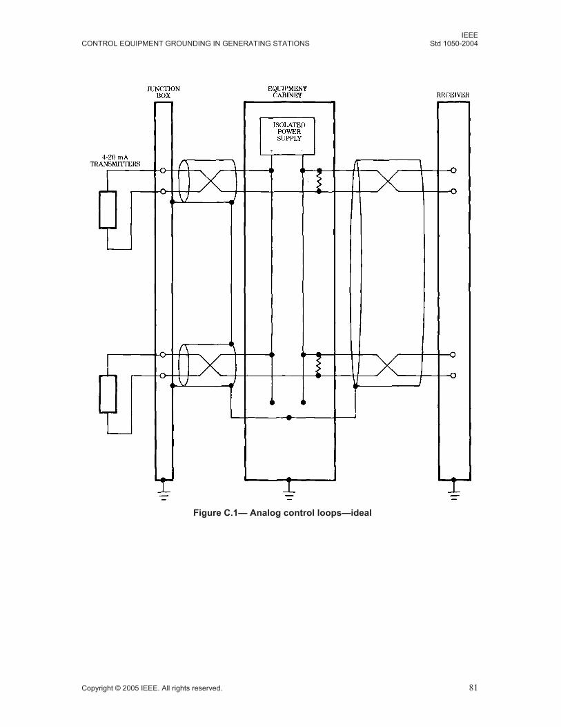
IEEECONTROL EQUIPMENT GROUNDING IN GENERATING STATIONS Std 1050-2004
Figure C.1— Analog control loops—ideal
Copyright © 2005 IEEE. All rights reserved. 81
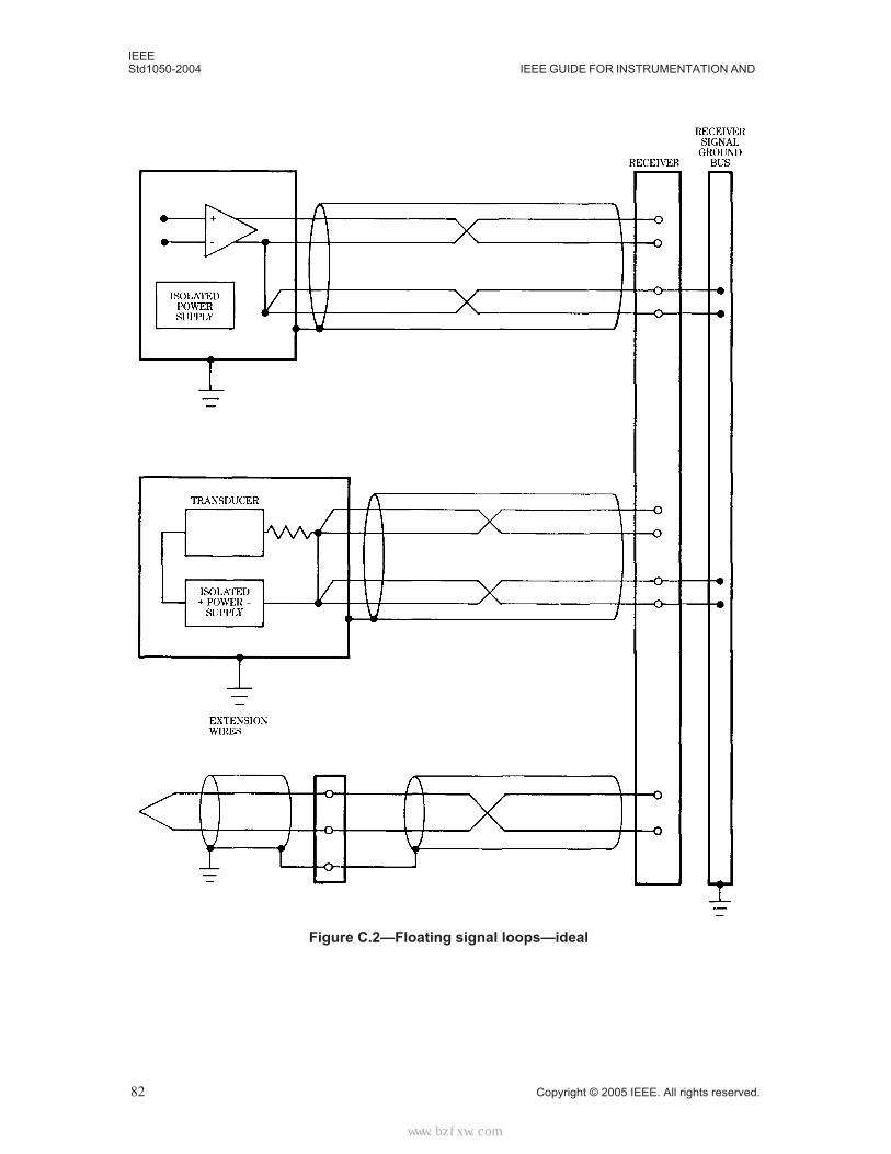
IEEEStd1050-2004 IEEE GUIDE FOR INSTRUMENTATION AND
Figure C.2—Floating signal loops—ideal
82 Copyright © 2005 IEEE. All rights reserved.
标准分享网 www.bzfxw.com 免费下载
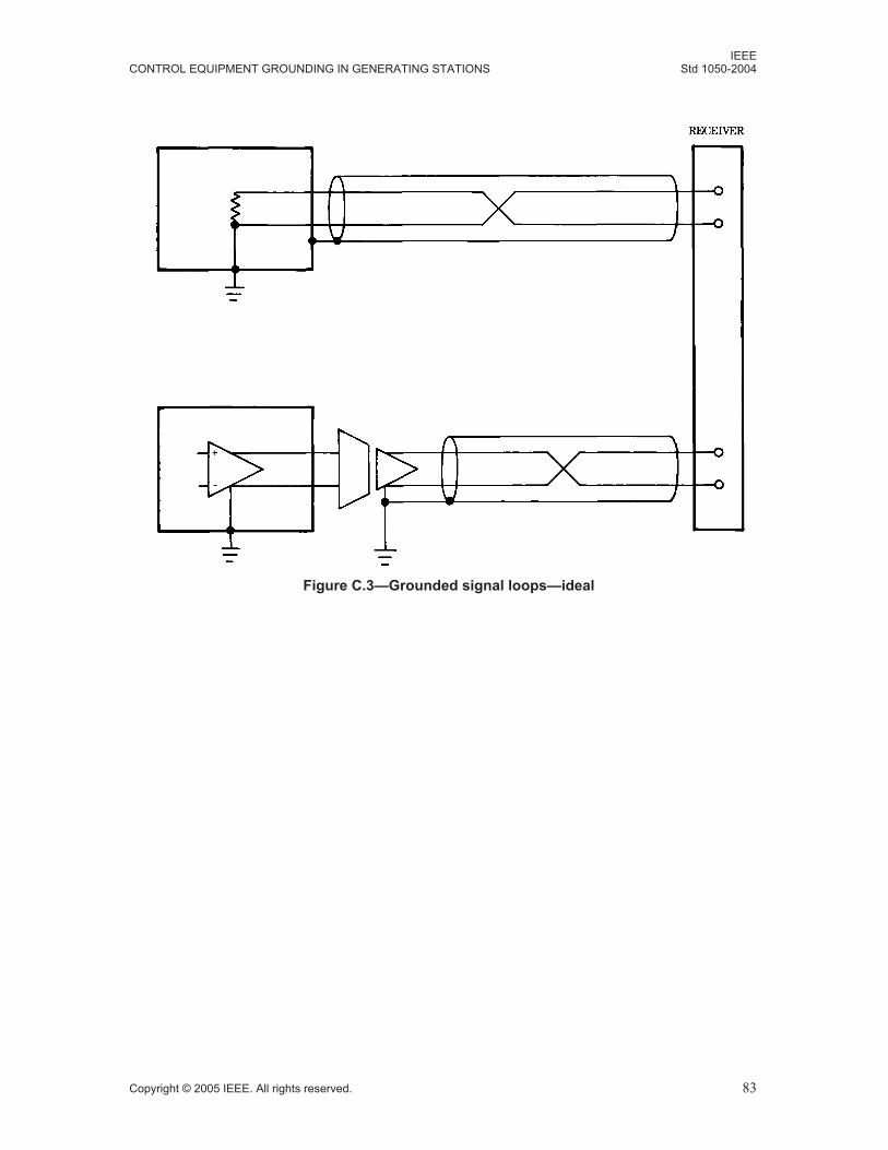
IEEECONTROL EQUIPMENT GROUNDING IN GENERATING STATIONS Std 1050-2004
Figure C.3—Grounded signal loops—ideal
Copyright © 2005 IEEE. All rights reserved. 83
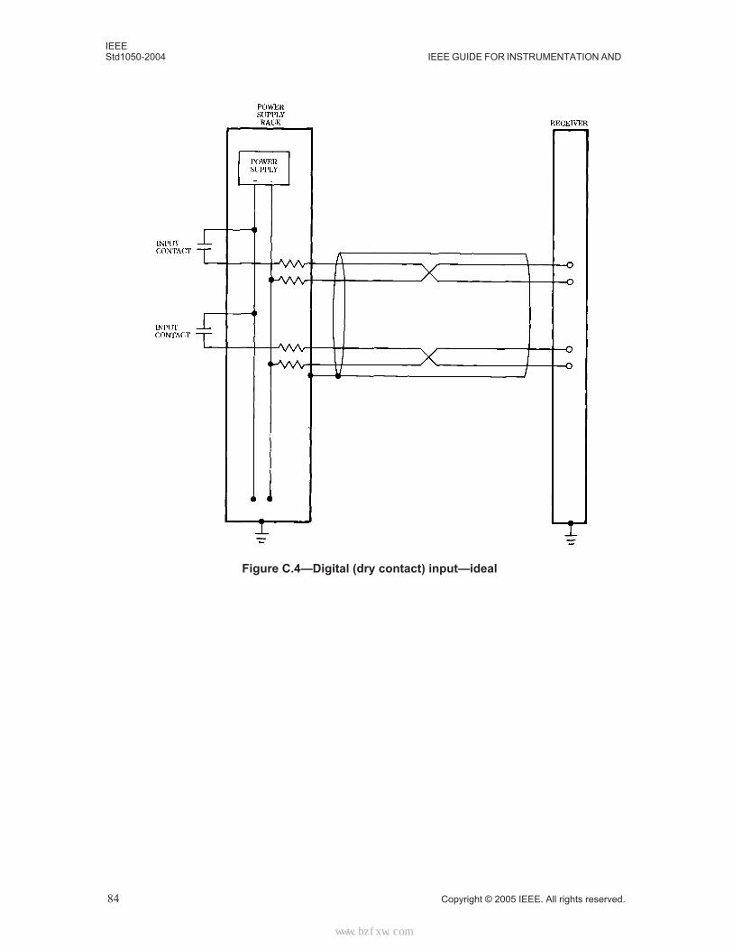
IEEEStd1050-2004 IEEE GUIDE FOR INSTRUMENTATION AND
Figure C.4—Digital (dry contact) input—ideal
84 Copyright © 2005 IEEE. All rights reserved.
标准分享网 www.bzfxw.com 免费下载
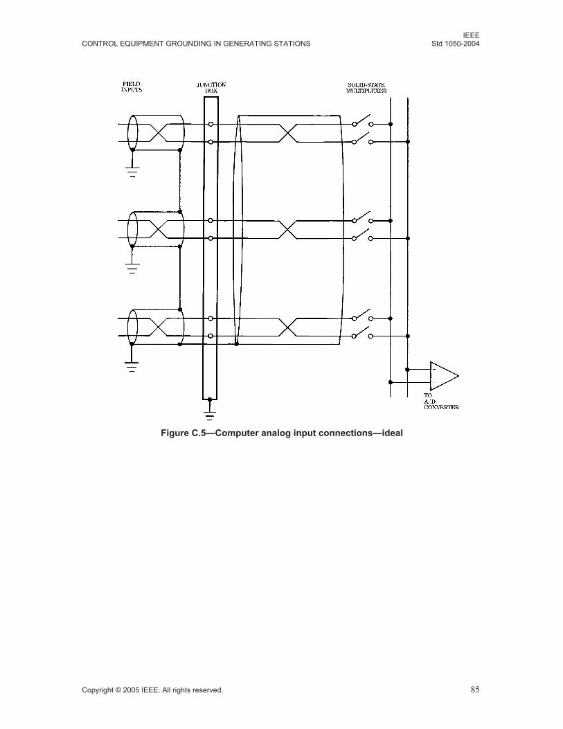
IEEECONTROL EQUIPMENT GROUNDING IN GENERATING STATIONS Std 1050-2004
Figure C.5—Computer analog input connections—ideal
Copyright © 2005 IEEE. All rights reserved. 85
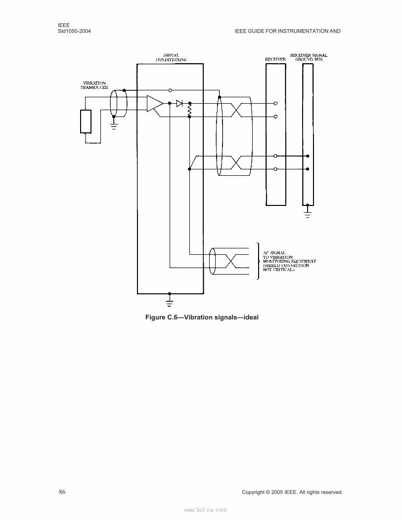
IEEEStd1050-2004 IEEE GUIDE FOR INSTRUMENTATION AND
Figure C.6—Vibration signals—ideal
86 Copyright © 2005 IEEE. All rights reserved.
标准分享网 www.bzfxw.com 免费下载
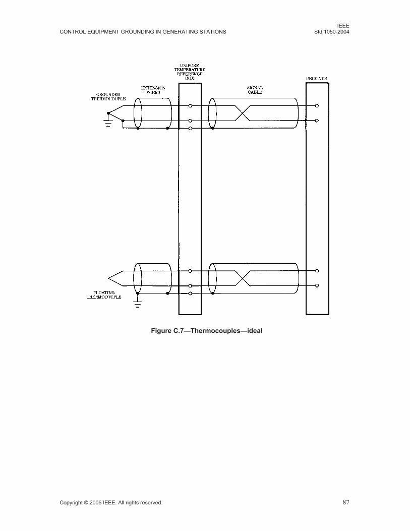
IEEECONTROL EQUIPMENT GROUNDING IN GENERATING STATIONS Std 1050-2004
Figure C.7—Thermocouples—ideal
Copyright © 2005 IEEE. All rights reserved. 87
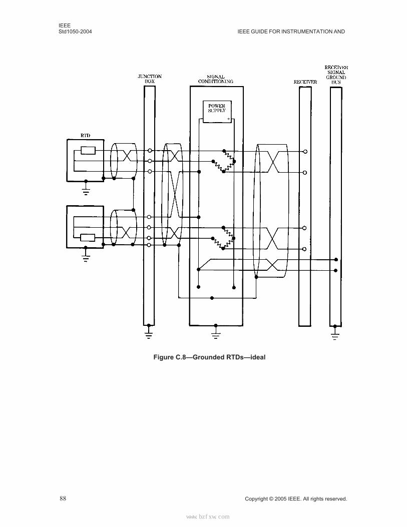
IEEEStd1050-2004 IEEE GUIDE FOR INSTRUMENTATION AND
Figure C.8—Grounded RTDs—ideal
88 Copyright © 2005 IEEE. All rights reserved.
标准分享网 www.bzfxw.com 免费下载
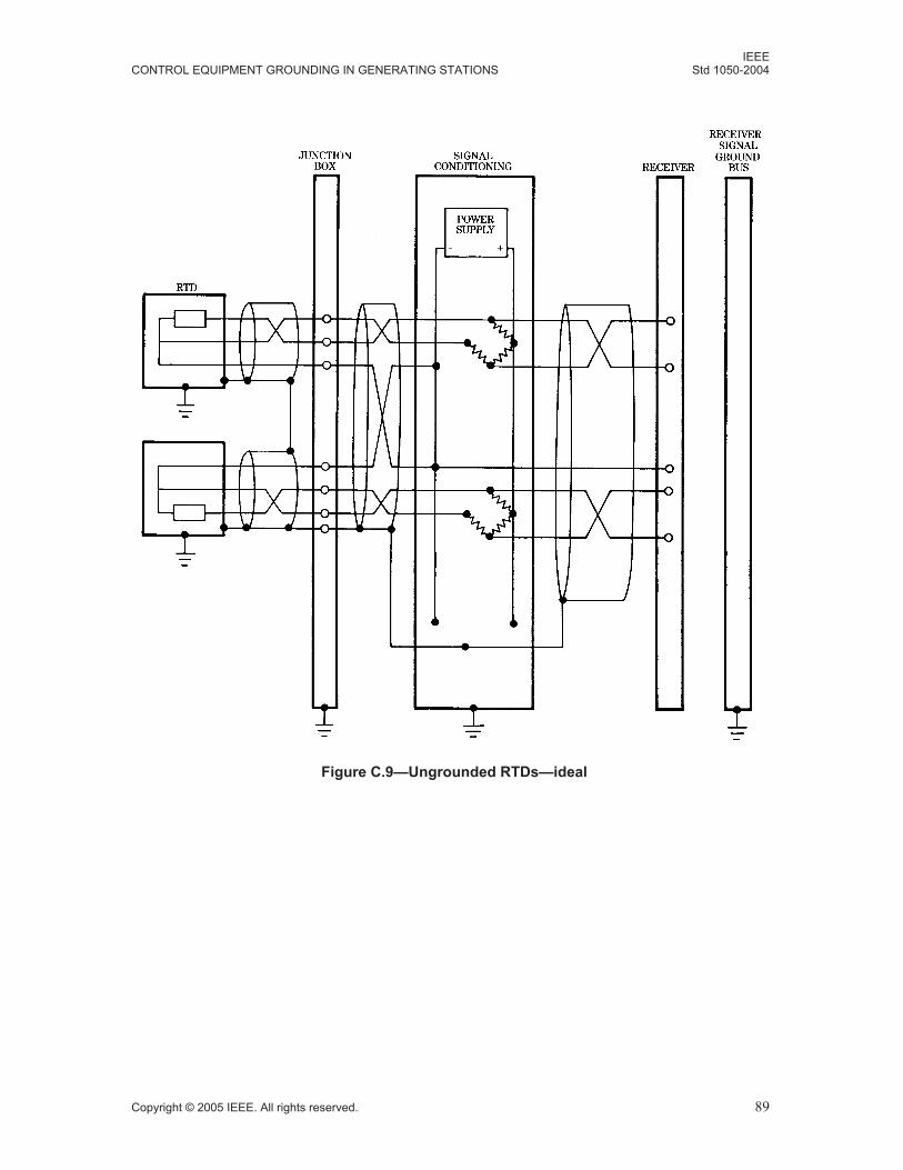
IEEECONTROL EQUIPMENT GROUNDING IN GENERATING STATIONS Std 1050-2004
Figure C.9—Ungrounded RTDs—ideal
Copyright © 2005 IEEE. All rights reserved. 89
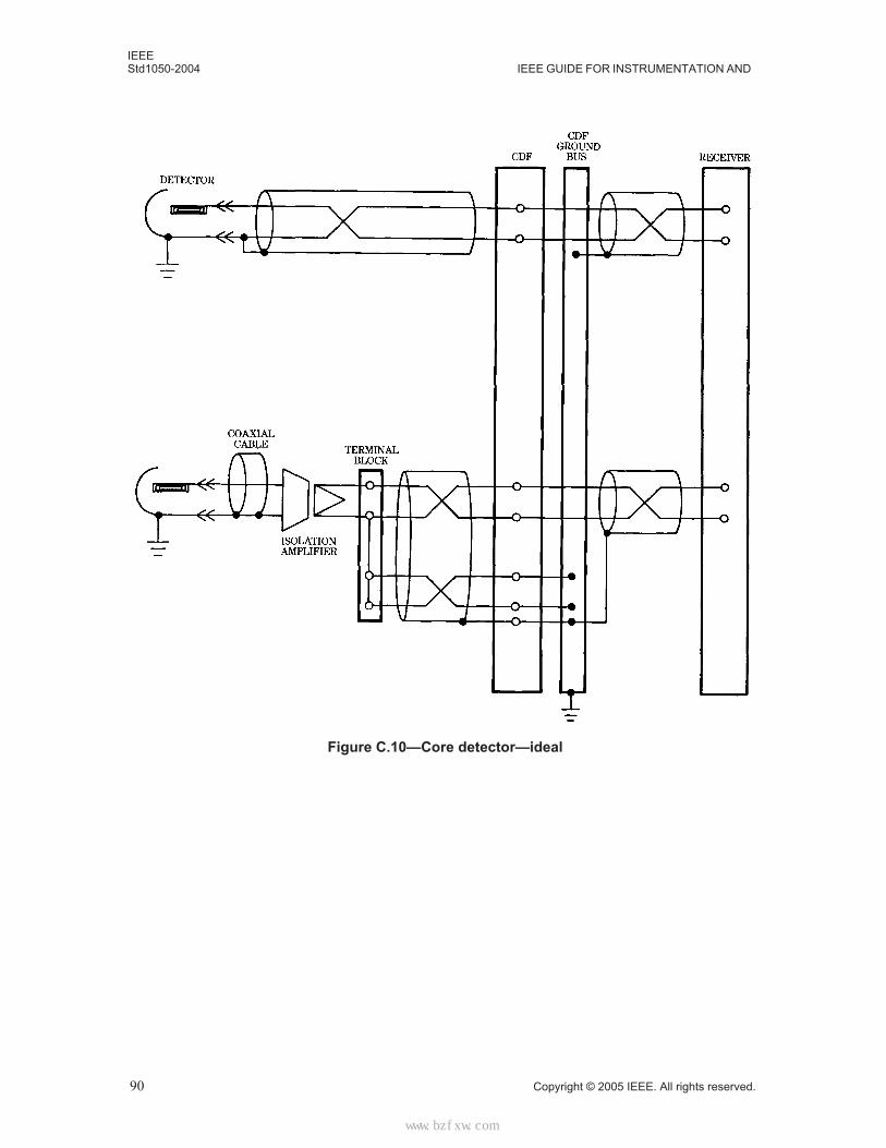
IEEEStd1050-2004 IEEE GUIDE FOR INSTRUMENTATION AND
Figure C.10—Core detector—ideal
90 Copyright © 2005 IEEE. All rights reserved.
标准分享网 www.bzfxw.com 免费下载
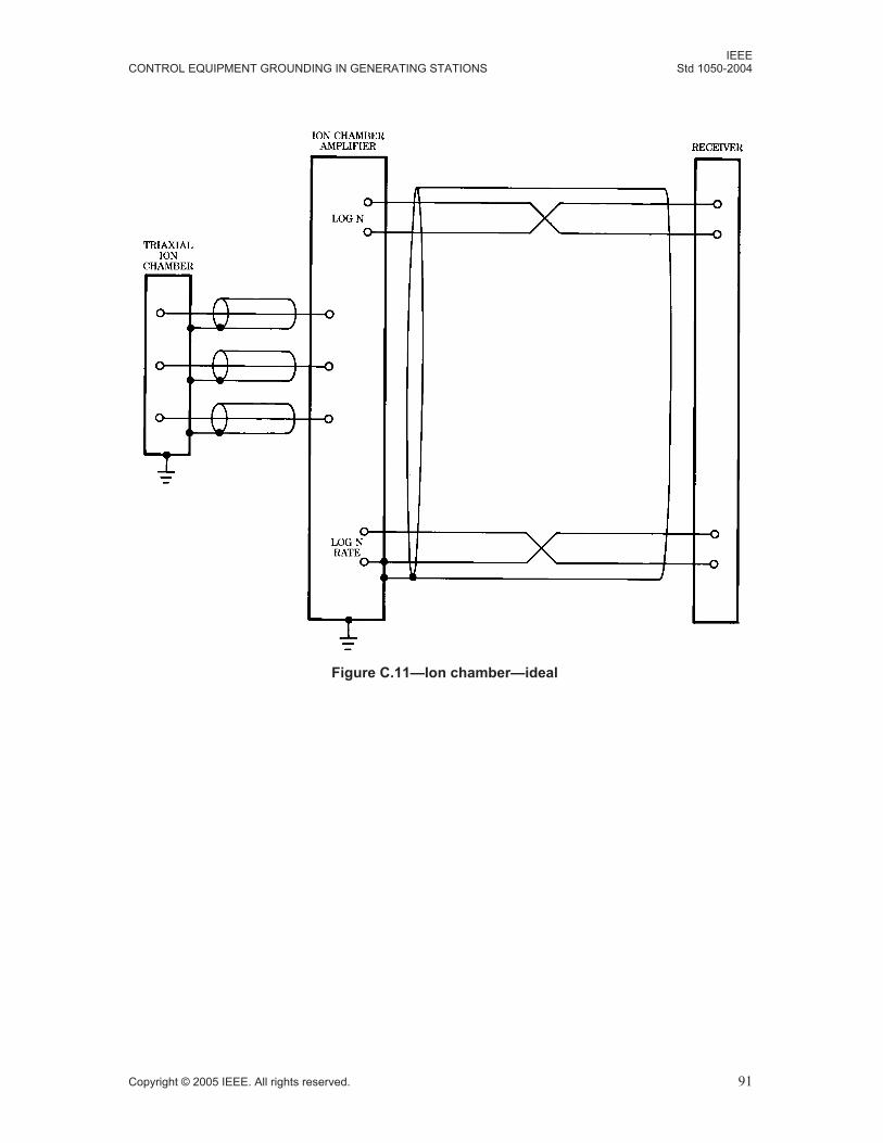
IEEECONTROL EQUIPMENT GROUNDING IN GENERATING STATIONS Std 1050-2004
Figure C.11—Ion chamber—ideal
Copyright © 2005 IEEE. All rights reserved. 91
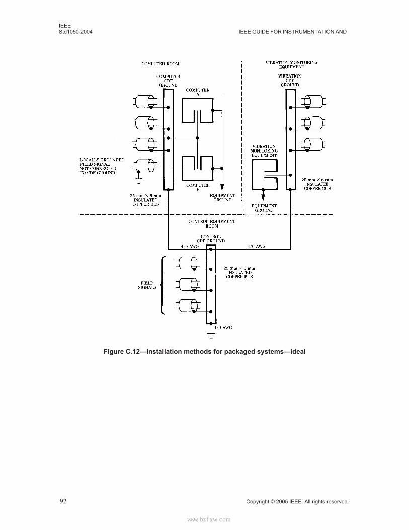
IEEEStd1050-2004 IEEE GUIDE FOR INSTRUMENTATION AND
Figure C.12—Installation methods for packaged systems—ideal
92 Copyright © 2005 IEEE. All rights reserved.
标准分享网 www.bzfxw.com 免费下载
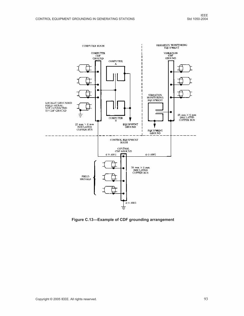
IEEECONTROL EQUIPMENT GROUNDING IN GENERATING STATIONS Std 1050-2004
Figure C.13—Example of CDF grounding arrangement
Copyright © 2005 IEEE. All rights reserved. 93


![I13presentation.ppt [Read-Only] · [7] Std. 80™-2000, IEEE Guide for Safety in AC Substation Grounding [8] Std. 142™-1991, IEEE Recommended Practice for Grounding of Industrial](https://static.fdocuments.us/doc/165x107/5ead97c98d6c8974e477813a/read-only-7-std-80a-2000-ieee-guide-for-safety-in-ac-substation-grounding.jpg)