IEEE SF Bay Area MEMS & Sensors Chapter
42
IEEE SF Bay Area MEMS & Sensors Chapter November 19, 2014 http://sites.ieee.org/scv-mems/ 1
Transcript of IEEE SF Bay Area MEMS & Sensors Chapter

IEEE SF Bay Area MEMS & Sensors Chapter
November 19, 2014
http://sites.ieee.org/scv-mems/1

Past Meetings
2 11/22/2014
2014 TITLE Guests IEEE TotalJan. 22nd Emerging Trillion Sensors Movement (Dr. Janusz Bryzek) 39 41 80Feb. 26th FBAR and FMOS Technology from a MEMS Perspective
(Dr. Stephen Gilbert)Advanced Metal Eutectic Bonding for High Volume MEMS (Sumant Sood)
35 35
70Mar. 18th Coupled-Filed MEMS Simulations (Dr. Metin Ozen) 25 7 32April 30th MEMS Wars: A New Hope (Dr. Kurt Petersen) 37 39 76May 28th MEMS in SEMI – The Role of a Global Association in Advancing
the MEMS Industry (Bettina Weiss)11 12
23June 25th MEMS on Alternate Substrates: A Case Study with Biometric
Sensors (Dr. KG Ganapathi)21 29
50July 23rd AdCom/Volunteers meeting 11 10 21Aug. 27th RF MEMS: From Research to Products (Prof. Gabriel Rebeiz) 30 46 76Sept. 24th IEEE MEMS Happy Hour (No invited talk). 12 12 24Oct. 22nd MEMS-enabled microscopes for in-vivo studies of cancer biology 29 31 60
Total 250 262 512

Officers and Program Committee
The MEMS and Sensors Chapter is run by volunteers organized as Officers (elected every year), Program Committee, and Advisory Board. If you are interested in volunteering, please send an email to [email protected].
Officers:Chair: Dr. Ramesh Ramadoss, Senior Manager, FormFactor Inc.Vice-Chair: Dr. Yan Du, Manager, Qualcomm MEMS Technologies Inc.Secretary: Dr. Gavin Ho, President, NanoFab Corp.Treasurer: Mr. Jeremie Dalton, Staff Engineer, Enovix Inc.Workshop Chair: Mr. Brent Lunceford, Advanced Product Development, 3M.
Program Committee:Dr. John Lee, Associate Professor, Mechanical Engineering, San José State UniversityDr. Mary Ann Maher, President, SoftMEMS Inc.Dr. Nisarga Naik, Research Scientist, Intel Labs.Dr. Hojr Sedaghat-Pisheh, Hardware Engineer/Manager, Google Inc.Mr. Sumant Sood, Product Marketing Manager, KLA-Tencor Inc.Amber Sun, Senior Engineer, Qualcomm Inc.Dr. Youmin Wang, Postdoc, UC Berkeley.Dr. Ernest Yen, MEMS Researcher, Texas Instruments Inc.Dr. Ningning Zhou, Staff Engineer, Qualcomm MEMS Technologies.
Advisory Board:Dr. Janusz Bryzek, TSensors Summit.Mr. Gene Burk, Consultant, IMT Inc.Dr. Leslie Field, Founder, SmallTech Consulting LLC; Consulting Professor, EE, Stanford University.Dr. Jim Knutti, President/CEO, Acuity Inc.Dr. Kurt Petersen, President, KP-MEMS Inc.3

Meeting Sponsor
4 11/22/2014
Complimentary food and refreshments sponsored by SoftMEMS Inc.
Thanks to Dr. Mary Ann Maher,
President/CEO
Upcoming Meetings
Feb. 25th, 2015 (Wednesday) 7:45 PM to 8:45 PM. Note: NEW LOCATION!!!Title: Building Successful MEMS Company: From Start to IPOSpeaker: Mr. Steve Nasiri, Nasiri VenturesLocation: Texas Instruments Building E Conference Center, 2900 Semiconductor Dr., Santa Clara, CA 95052 (Directions)Food: Pizza and beverages will be available at 7:15 pm for a $5 donation at the door.Sponsor: Sponsorship opportunities are available. Interested parties please email [email protected]
Mar. 25th, 2015 (Wednesday) 5:30 PM to 7:30 PM. Online registration coming soon.IEEE MEMS and Sensors Happy HourLocation: Steelhead Brewing Company, 333 California Drive, Burlingame, CA 94010This is a no-host event. Please pay for your own food and drinks.Sponsor: Sponsorship opportunities are available. Interested parties please email [email protected]
5 11/22/2014

Invited talk by Mr. Holger Doering
6 11/22/2014
He is responsible for Production, Process Engineering, IT, Assembly, Test, and Facilities Management. He started at ELMOS in 1995 as a Process Engineer and became Production Engineering Manager in 1997. From 1999 he was responsible for Production, Process Engineering and Equipment Maintenance in the Plasma-Module of the ELMOS fab. In 2003 he began to transfer the 0.8 μm process from the 6-inch fab in Dortmund to the 8-inch line of the joint ELMOS/ Fraunhofer IMS fab in Duisburg and in 2005 became responsible for the complete 8-inch Operations in Duisburg.
Holger holds a diploma in Electrical Engineering from the University of Dortmund (Germany) with a focus on semiconductor manufacturing. His diploma thesis work was carried out at ELMOS in 1994 where he developed a CMOS-compatible process module to produce monolithic integrated piezoresistive pressure sensors in a EU-funded project. .
Nov. 19th, 2014 (Wednesday) 7:45 PM to 8:45 PM.Title: Innovative Pressure Sensing Solutions.Speaker: Mr. Holger Doering, COO, Silicon Microstructures, Inc.
Holger Doering is the Chief Operating Officer (COO) at Silicon Microstructures Inc (SMI). He joined SMI in 2007 as a Consultant in Operations, then took over the VP Operations position in 2008 and was promoted to COO in 2011.

Innovative Pressure Sensing Solutions
Abstract: Silicon Microstructures Inc (SMI) is a premier semiconductor sensor company developing and manufacturing MEMS-based pressure sensors for automotive, medical, and industrial markets. It has a long history rooted in Silicon Valley since 1991. This talk will present the recent developments in pressure sensor R&D and production at SMI. It will cover the following aspects:1. Company overview on products, R&D and Manufacturing capabilities2. DRIE etch is essential for pressure sensor miniaturization. This talk
will present SMI ultra-small pressure sensor development with DRIE process.
3. Automated Optical Inspection (AOI) for defect detection in MEMS devices. This talk will cover the application criteria and inspection capabilities.
7

Innovative Pressure
Sensing Solutions
Created by Dr. Shaoxin Lu, Abhishek Davray, Raul Figueroa and Holger Doering
November 18, 2014
Supporting customer success in Automotive, Medical and Industrial markets since 1991

CONFIDENTIAL © Silicon Microstructures, Inc. and Elmos Semiconductor AG all rights reserved. We reserve all rights such as copying and passing on to third parties.
27 45
131
161 29 37
SMI Mission
CONFIDENTIAL © Silicon Microstructures, Inc. and Elmos Semiconductor AG all rights reserved. We reserve all rights such as copying and passing on to third parties.
27 45
131
161 29 37
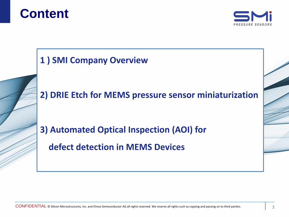
Content
1 ) SMI Company Overview
2) DRIE Etch for MEMS pressure sensor miniaturization
3) Automated Optical Inspection (AOI) for
defect detection in MEMS Devices
3
CONFIDENTIAL © Silicon Microstructures, Inc. and Elmos Semiconductor AG all rights reserved. We reserve all rights such as copying and passing on to third parties.
27 45
131
161 29 37
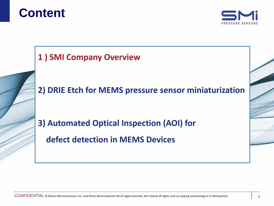
Content
1 ) SMI Company Overview
2) DRIE Etch for MEMS pressure sensor miniaturization
3) Automated Optical Inspection (AOI) for
defect detection in MEMS Devices
4

CONFIDENTIAL © Silicon Microstructures, Inc. and Elmos Semiconductor AG all rights reserved. We reserve all rights such as copying and passing on to third parties.
27 45
131
161 29 37
Pioneering Innovation and Expertise
Leader in MEMS-based Pressure Sensing Solutions
• Lowest pressure: down to 4 mbar range (1.5” H2O) • Media Resistant: noble metallization w/ backside entry. • Smallest size: down to 0.9 mm × 0.25 mm × 75 µm
23 years of development and manufacturing expertise • 100% subsidiary of Elmos Semiconductor AG
(Germany) • More than 500M sensors sold into Automotive,
Medical, Consumer, HVAC and Industrial markets
Captive Wafer Fab in Silicon Valley (USA) All functions in one location:
• R&D, Process Development • Logistics & Quality Control
5
Silicon Valley

CONFIDENTIAL © Silicon Microstructures, Inc. and Elmos Semiconductor AG all rights reserved. We reserve all rights such as copying and passing on to third parties.
27 45
131
161 29 37
Company History
6
1991
Founded in Fremont
(CA)
2001
Acquired by
elmos in
Dortmund (Germany)
2002
Acquisition of MEMS fab,
relocation to Milpitas
(CA)
2004
Start of 6“ MEMS
production.
2006
TS16949 Certification
SO-16 package platform
2007
SO-8 package platform
2013
New Product Introductions
SM9541
2012
Die Portfolio Refresh
2014
New Product Introductions
SM68E

CONFIDENTIAL © Silicon Microstructures, Inc. and Elmos Semiconductor AG all rights reserved. We reserve all rights such as copying and passing on to third parties.
27 45
131
161 29 37
Process & Quality - Manufacturing Processes
Superior Quality and Long-Term Supply
ISO/TS 16949:2009 (Automotive)
ISO 9001:2008
ISO 14001:2004 (Environmental)
7
Foundry
Create electrical components
Etch Plant
Create mechanical components
Die Plant
• Final probe
• Singulation
• Inspection
Packaging
Housing of pressure sensor and ASIC
Test
• Calibration & compensation
• Final test
Frontend Processes Backend Processes Assembly & Test
State of the Art MEMS Manufacturing
Fully Equipped Wafer Fab

CONFIDENTIAL © Silicon Microstructures, Inc. and Elmos Semiconductor AG all rights reserved. We reserve all rights such as copying and passing on to third parties.
27 45
131
161 29 37
Low Pressure Sensor: 4 mbar
SMI patented Technologies
Signal-Conditioned
Ultra Small
Low Pressure
Product Overview - Areas of Expertise
8
Harsh Environment
Custom Design
Ultra-Small Die and Packaged Sensor for OEM Use
Harsh Environment Pressure Sensor Die
Dual Chip Intelligent Pressure Sensor, SO-16 Package
Custom Pressure Sensor for Arterial Catheter:
( 900 x 240 x 75 µm)
Typical Applications:
Medical (CPAP), Industrial (HVAC)
Typical Applications:
Automotive (TPMS),
Industrial (Barometric)
Typical Applications:
Automotive transmission,
Diesel Particle Filter (DPF) Exhaust Gas Recirc. (EGR)
Typical Applications:
Respiration Ventilators
HVAC & Pressure Transmitters
0.9mm
0.24 mm

CONFIDENTIAL © Silicon Microstructures, Inc. and Elmos Semiconductor AG all rights reserved. We reserve all rights such as copying and passing on to third parties.
27 45
131
161 29 37
Markets and Applications
9
Automotive
Respiration
• CPAP
• Ventilation
Hospital Beds
Fluid Evacuation
Blood Pressure
Wound Therapy
HVAC
VAV Controllers
Pressure Transmitters
Liquid Level & Pressure
Barometric Pressure
Process Control
Refrigeration
Industrial Medical
Tire Pressure Monitoring Systems (TPMS)
Manifold Air Pressure (MAP)
Diesel Particulate Filter (DPF)
Exhaust Gas Recirculation (EGR)
Oil Pressure
Side Air Bag
Transmission Oil Pressure
Seat Ergonomics

CONFIDENTIAL © Silicon Microstructures, Inc. and Elmos Semiconductor AG all rights reserved. We reserve all rights such as copying and passing on to third parties.
27 45
131
161 29 37
10
Applications - Medical
Sleep Apnea Treatment
• CPAP (Continuos Positive Airway Pressure)
• Sleep disorder with abnormal pauses in breathing
• CPAP uses mild air pressure to keep an airway open
-> Feedback of applied air pressure in the mask
-> µC manages compressor to generate
required pressure
Low Pressure
Interventional Cardiology
FFR (Fractional Flow Reserve) guide-wire based procedure
-> accurately measure blood pressure and flow
through a specific part of the coronary artery
-> assess whether or not to perform angioplasty
and / or stenting on "intermediate" blockages.
-> FFR reduces procedure cost & increases success rate
-> Biocompatibility and blood as harsh environment
Ultra Small Custom Sensors

CONFIDENTIAL © Silicon Microstructures, Inc. and Elmos Semiconductor AG all rights reserved. We reserve all rights such as copying and passing on to third parties.
27 45
131
161 29 37
11
Applications - Industrial
Pressure Transmitters/HVAC
• HVAC (Heating, Venting, Air Conditioning)
• Differential pressure transmitters to detect
over- / under- and differential pressure.
-> Monitoring and control of ventilation
and air-conditioning, fans and filters.
-> requires measurement of very
low-pressure signals
Valve Positioner
• Intelligent digital valve controllers
• Remote ambient pressure measurement
-> valve positioning & monitoring of supply pressure
-> support advances in building technology
and energy efficiency mandates
Low Pressure
Ambient Pressure
CONFIDENTIAL © Silicon Microstructures, Inc. and Elmos Semiconductor AG all rights reserved. We reserve all rights such as copying and passing on to third parties.
27 45
131
161 29 37
12
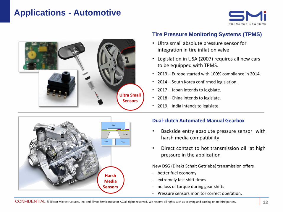
Applications - Automotive
Tire Pressure Monitoring Systems (TPMS)
• Ultra small absolute pressure sensor for integration in tire inflation valve
• Legislation in USA (2007) requires all new cars to be equipped with TPMS.
• 2013 – Europe started with 100% compliance in 2014.
• 2014 – South Korea confirmed legislation.
• 2017 – Japan intends to legislate.
• 2018 – China intends to legislate.
• 2019 – India intends to legislate.
Ultra Small Sensors
Dual-clutch Automated Manual Gearbox
• Backside entry absolute pressure sensor with harsh media compatibility
• Direct contact to hot transmission oil at high pressure in the application
New DSG (Direkt Schalt Getriebe) transmission offers
- better fuel economy
- extremely fast shift times
- no loss of torque during gear shifts
- Pressure sensors monitor correct operation.
Harsh Media
Sensors

CONFIDENTIAL © Silicon Microstructures, Inc. and Elmos Semiconductor AG all rights reserved. We reserve all rights such as copying and passing on to third parties.
27 45
131
161 29 37
Finite Element Modeling
• Optimize structure and predict results
• Mechanical stress and strain
• Resistance and temperature
Design & Simulation of Advanced Pressure Sensors
Process and Device Modeling
• Determine doping profiles from process
• Predict electrical characteristics of devices
• 2D device modeling
Design Rule Checking of Device Layout
•Verify placement tolerances of electrical components
• Check predicted distances between electrical and
mechanical components of MEMS structures
13
CONFIDENTIAL © Silicon Microstructures, Inc. and Elmos Semiconductor AG all rights reserved. We reserve all rights such as copying and passing on to third parties.
27 45
131
161 29 37
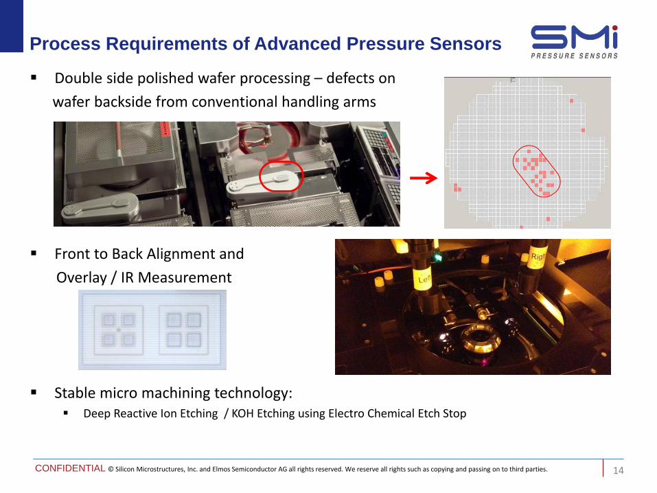
Process Requirements of Advanced Pressure Sensors
Double side polished wafer processing – defects on
wafer backside from conventional handling arms
14
Front to Back Alignment and
Overlay / IR Measurement
Stable micro machining technology: Deep Reactive Ion Etching / KOH Etching using Electro Chemical Etch Stop

CONFIDENTIAL © Silicon Microstructures, Inc. and Elmos Semiconductor AG all rights reserved. We reserve all rights such as copying and passing on to third parties.
27 45
131
161 29 37
Content
1 ) SMICompany Overview
2) DRIE Etch for MEMS pressure sensor miniaturization
3) Automated Optical Inspection (AOI) for
defect detection in MEMS Devices
15

CONFIDENTIAL © Silicon Microstructures, Inc. and Elmos Semiconductor AG all rights reserved. We reserve all rights such as copying and passing on to third parties.
27 45
131
161 29 37
DRIE – Deep Reactive Ion Etching
Bosch Process
• Silicon anisotropic etching based on etch/deposition cycle by cycling SF6/C4F8
• Silicon etch in SF6 cycle
• Passivation of sidewalls with polymer in C4F8 cycle
16

CONFIDENTIAL © Silicon Microstructures, Inc. and Elmos Semiconductor AG all rights reserved. We reserve all rights such as copying and passing on to third parties.
27 45
131
161 29 37
DRIE vs KOH Etch
Benefits for DRIE
Precise control of membrane thickness
Area reduction for sensors
Bigger mounting surface, no constraint wafer necessary
Better accuracy / repeatability
DRIE
KOH
KOH DRIE
Membrane Thickness Controlled by Etch rate / Etch stop
Defined by SOI starting material
Sensor Size Bigger (with sidewall slope)
Smaller (vertical sidewall)
Mounting Area (% of die)
Smaller (with sidewall slope)
Bigger ( vertical sidewall)
Accuracy/Repeatability Worse ( TTV, Etch rate variation)
Better (SOI material control)
Cost Less expensive
More expensive (factor 3 x variable cost)
Throughput Batch process (factor 2 x faster than DRIE)
Single wafer process
17

CONFIDENTIAL © Silicon Microstructures, Inc. and Elmos Semiconductor AG all rights reserved. We reserve all rights such as copying and passing on to third parties.
27 45
131
161 29 37
Products at SMI that benefit from DRIE
Ultra small pressure sensors (SM68) for TPMS applications:
-> Pressure range from 15 -150 psi
-> DRIE formed cavity on backside enabling very small sensor design on SOI
-> size reduction of about 60% compared to non DRIE etched sensors
SM95 wafer in front of a lamp showing semitransparent membranes formed by DRIE
SM68 sensor SM68 sensor DRIE backside cavities
18
Ultra Low pressure sensors (SM95) for medical and industrial applications
-> Pressure range from 0.15 to 1.5psi
-> Backside cavity and pressure range adjustment with DRIE process
Covered under Patents US 7,111,518 and US 8,381,596 B2

CONFIDENTIAL © Silicon Microstructures, Inc. and Elmos Semiconductor AG all rights reserved. We reserve all rights such as copying and passing on to third parties.
27 45
131
161 29 37
Compensation of DRIE non-uniformities
CD / Overlay run-out towards the wafer edge
- > DRIE CD gets bigger close to wafer edge due to loading effect
- > Cavity shifts in the radial direction at wafer edge due to “outside effect ”
Edge compensation in mask layout to improve CD/Overlay uniformity
Typical CD distribution in X-direction Typical cavity overlay distribution in X-direction
19

CONFIDENTIAL © Silicon Microstructures, Inc. and Elmos Semiconductor AG all rights reserved. We reserve all rights such as copying and passing on to third parties.
27 45
131
161 29 37
DRIE formed cavities for pressure sensors
Buried Cavity Technology --- DRIE reference cavity formed and buried in wafer before sensor /CMOS Foundry process
Comparison Classic DRIE Approach Buried Cavity Technology
Process sequence
Sensor foundry -> DRIE
DRIE -> Sensor foundry
Etch time Long, through wafer etch low throughput
Short, shallow cavity etch high throughput
Cavity CD Variation across wafer Precise CD control
Cavity Overlay
Variation across wafer Minimized Overlay error
Edge excl. Zone
Exclusion zone due to DRIE variance
Nearly no exclusion zone required
CMOS compatibility
Plasma Damage could impact CMOS circuits
Compatible
IR Image
Sensing bridge formed on pre-defined membrane
Optical Image
20
CONFIDENTIAL © Silicon Microstructures, Inc. and Elmos Semiconductor AG all rights reserved. We reserve all rights such as copying and passing on to third parties.
27 45
131
161 29 37
Content
1 ) SMICompany Overview
2) DRIE Etch for MEMS pressure sensor miniaturization
3) Automated Optical Inspection (AOI) for
defect detection in MEMS Devices
21

CONFIDENTIAL © Silicon Microstructures, Inc. and Elmos Semiconductor AG all rights reserved. We reserve all rights such as copying and passing on to third parties.
27 45
131
161 29 37
Automated Optical Inspection (AOI)
• Automated Optical Inspection (AOI)
scans the wafer surface and
automatically detects defects and
classifies them
• ICOS, originating in Belgium and
acquired in 2008 by KLA Tencor, built
the equipment
• The system is equipped with one
central loader and two inspection
modules with high speed line cameras
22

CONFIDENTIAL © Silicon Microstructures, Inc. and Elmos Semiconductor AG all rights reserved. We reserve all rights such as copying and passing on to third parties.
27 45
131
161 29 37
Importance of visual inspection for MEMS devices
Defects that cannot be caught by electrical tests and cause reliability / performance impacts
Bond Void on the backside -> could cause a leak for absolute pressure sensors
Cracks in Membrane -> falsifies the pressure signal -> reliability problem
23

CONFIDENTIAL © Silicon Microstructures, Inc. and Elmos Semiconductor AG all rights reserved. We reserve all rights such as copying and passing on to third parties.
27 45
131
161 29 37
Importance of visual inspection for MEMS devices
Defects that cannot be caught by electrical tests and cause reliability / performance impacts
Mis-shaped cavity -> influence on pressure non-linearity -> modified sensitivity
Defects in backside metallization -> could weaken eutectic bond -> reliability problem
24

CONFIDENTIAL © Silicon Microstructures, Inc. and Elmos Semiconductor AG all rights reserved. We reserve all rights such as copying and passing on to third parties.
27 45
131
161 29 37
Criteria and methods to detect different defects
Frontside Inspection
Metal Area
Inspects for scratches and contamination in the metal region
Example for the criteria used to detect the defect
Metal Regions
Membrane area
25
Membrane Area
Inspects for fractures and contamination on the membrane
Example

CONFIDENTIAL © Silicon Microstructures, Inc. and Elmos Semiconductor AG all rights reserved. We reserve all rights such as copying and passing on to third parties.
27 45
131
161 29 37
Criteria and methods to detect different defects
Backside Inspection
Bond Void Area
Inspects for voids in the bond interface outside the cavity area
Example
Bond Void Region
Diaphragm Region
26
Diaphragm Area
Inspects for cracks and contamination inside the diaphragm region
Example

CONFIDENTIAL © Silicon Microstructures, Inc. and Elmos Semiconductor AG all rights reserved. We reserve all rights such as copying and passing on to third parties.
27 45
131
161 29 37
Inspection at different stages
KOH etched Backside Pre – Metal Inspection
Focus on specific defects in the different stages of the process
Bond interface and membrane defects after bonding
Defects in backside metal that influence eutectic bond
Inspection after sawing for saw chipping and cracks
After Metal deposition for Eutectic Bond
Backside after sawing -> picture more blurry
DRIE etched Backside before sawing
27

CONFIDENTIAL © Silicon Microstructures, Inc. and Elmos Semiconductor AG all rights reserved. We reserve all rights such as copying and passing on to third parties.
27 45
131
161 29 37
Inspection record to document quality
Defect was not on the Die at AOI
Reassure customer of excellent quality
-> Defect must have occurred at customer
site, finish with 5D report
SM68 Sensor Image at SMI
Sensor Image at Customer Site
28

CONFIDENTIAL © Silicon Microstructures, Inc. and Elmos Semiconductor AG all rights reserved. We reserve all rights such as copying and passing on to third parties.
27 45
131
161 29 37
Defect Reduction Program
Screening with AOI after different steps in the process
Correlation of defect to certain equipment used at that point
Novellus Paddle
Wafer flat
pins Lift pins 1. run
Tegal Paddle
29
Lift pins 2. run
Tegal Paddle

CONFIDENTIAL © Silicon Microstructures, Inc. and Elmos Semiconductor AG all rights reserved. We reserve all rights such as copying and passing on to third parties.
27 45
131
161 29 37
Classification and Yield Analysis using Pareto
Automated defect classification - type of defect - area where it is detected
Shortcut keys for fast Operator reclassification during review
Visual of a wafer map for quick overview for Operators / Engineers
Reject Classification List
30
-> Basis for Pareto Analysis

CONFIDENTIAL © Silicon Microstructures, Inc. and Elmos Semiconductor AG all rights reserved. We reserve all rights such as copying and passing on to third parties.
27 45
131
161 29 37
Classification and Yield Analysis using Pareto
Column1 Column2
front side scratch 1.30%
front side contamination 1.03%
saw chip/cracked die 0.81%
front side KOH/ stained pad 0.27%
other/PCM/missing die 0.21%
delamination/bond void 0.20%
probe reject 0.19%
deep probe/ no probe marks 0.09%
back side contamination 0.01%
broken diaphragm 0.01%
uneven cavity 0.01%
Invalid 0.00%
etch pit 0.00%
discolored field front side 0.00%
back side scratch 0.00%
Pareto Analysis of Defect types improves the efficiency to increase Yield
Wafer level Yield has been improved at SMI by 5% as an average over all products in the last 3 years by using Automated Optical Inspection (some products up to 10%)
31

CONFIDENTIAL © Silicon Microstructures, Inc. and Elmos Semiconductor AG all rights reserved. We reserve all rights such as copying and passing on to third parties.
27 45
131
161 29 37
Automated Classification to reduce time & cost
Comparison Automated Optical Inspection 100% Operator Inspection
Front and Back Inspection on SM68 Sensor
~ 25 minutes machine time ~ 0 to 15min. Operator review time per wafer
~ 8 hours per wafer
Front and Back Inspection on SM95 Sensor
~ 10 minutes machine time ~ 5 to 15min. Operator review time per wafer
~ 2 hours per wafer
• The required throughput of > 40M sensors shipped per year would not have
been possible without AOI and not sacrificing quality assurance
• The cost per wafer and the required Operators were reduced significantly
• Customers rely on SMI`s quality inspection using AOI as an essential part
of the 0ppm automotive strategy
32
CONFIDENTIAL © Silicon Microstructures, Inc. and Elmos Semiconductor AG all rights reserved. We reserve all rights such as copying and passing on to third parties.
27 45
131
161 29 37
Acknowledgements
Special Thanks for preparing this presentation go to
Dr. Shaoxin Lu for the DRIE Etch portion
Abhishek Davray for the AOI portion
Dr. Steve Terry and Marc Konradt for Technology & Process
Raul Figueroa for the SMI Company Overview
33

Thank you !

CONFIDENTIAL © Silicon Microstructures, Inc. and Elmos Semiconductor AG all rights reserved. We reserve all rights such as copying and passing on to third parties.
27 45
131
161 29 37
Silicon Microstructures, Inc.
1701 McCarthy Blvd | Milpitas, CA 95035 | USA Phone: + 1 (408) 577-0100 | Fax: + 1 (408) 473-0123 [email protected] | www.si-micro.com
DISCLAIMER
This presentation contains forward-looking statements based on beliefs of Silicon
Microstructures‘ management. Such statements reflect the company‘s current views
with respect to future events and are subject to risks and uncertainties. Many factors
could cause the actual results to be materially different, including, among others,
changes in general economic and business conditions, changes in currency exchange
rates and interest rates, introduction of competing products, lack of acceptance of new
products or services and changes in business strategy. Actual results may vary
materially from those projected here. Silicon Microstructures does not intend or
assume any obligation to update these forward-looking statements.
35