IEEE SENSORS JOURNAL 1 Piezoelectric Polymer Transducer...
18
IEEE Proof IEEE SENSORS JOURNAL 1 Piezoelectric Polymer Transducer Arrays for Flexible Tactile Sensors Lucia Seminara, Luigi Pinna, Maurizio Valle, Member, IEEE, Laura Basiricò, Alberto Loi, Piero Cosseddu, Annalisa Bonfiglio, Alberto Ascia, Maurizio Biso, Alberto Ansaldo, Davide Ricci, and Giorgio Metta Abstract—In this paper, we propose a novel technological 1 approach for the implementation of large-area flexible artificial 2 skin based on arrays of piezoelectric polymer transducers. 3 Polyvinylidene fluoride (PVDF) transducers are chosen for the 4 high electromechanical transduction frequency bandwidth (up to 5 1 kHz). A low-cost and scalable technique for extracting PVDF 6 signals is used to directly provide the piezoelectric film with 7 patterned electrodes. If the skin is meant to cover large areas 8 of a robot body, specific requirements have to be fulfilled from 9 the point of view of the overall system and of the technology. 10 Experimental tests on the prototype skin modules demonstrate 11 the feasibility of the proposed approach and reveal the potential- 12 ity to build large area flexible skin. 13 Index Terms— PVDF piezoelectric transducers, artificial skin, 14 flexible sensors, ink jet printing, materials processing, robotic 15 skin. 16 I. I NTRODUCTION 17 A WIDE number of tactile sensors and systems have been 18 proposed over the last two decades and more [1]–[5]. 19 To effectively use artificial skin on robots (and not only), it 20 has been evidenced that the overall skin performance depends 21 not only on the characteristics of individual elements but 22 also on the system strategy to integrate the large number 23 of components/arrays and to cover large areas of the robot 24 body. Therefore, relevant technological issues must be faced 25 based on a system perspective. One of the main issues in 26 building skin systems is the deposition and patterning of 27 metal electrodes on the sensing film. Inkjet printing has been 28 chosen and it is proposed to deposit patterned metal layers 29 on the sensing film. The appeal of this technology lies in 30 Manuscript received April 27, 2013; accepted June 3, 2013. This work was supported in part by the European project “ROBOSKIN” about Skin-Based Technologies and Capabilities for Safe, Autonomous and Interactive Robots under Grant 231500. The associate editor coordinating the review of this paper and approving it for publication was Dr. Ravinder S. Dahiya. L. Seminara, L. Pinna, and M. Valle are with the Department of Telecommunications, Electronic, Electric and Naval Engineering, Univer- sity of Genoa, Genoa 65000-65480, Italy (e-mail: [email protected]; [email protected]; [email protected]). L. Basiricò, A. Loi, P. Cosseddu, and A. Bonfiglio are with the Department of Electrical and Electronic Engineering, University of Cagliari, Cagliari 09123, Italy (e-mail: [email protected]; [email protected]; [email protected]; [email protected]). A. Ascia, M. Biso, A. Ansaldo, D. Ricci, and G. Metta are with the Depart- ment of Robotics, Brain and Cognitive Sciences, Istituto Italiano di Tecnolo- gia, Genoa 16163, Italy (e-mail: [email protected]; [email protected]; [email protected]; [email protected]; [email protected]). Color versions of one or more of the figures in this paper are available online at http://ieeexplore.ieee.org. Digital Object Identifier 10.1109/JSEN.2013.2268690 its scalability to large area manufacturing through a maskless 31 approach [6]. 32 If the aim is to mimic the behavior of the human skin, 33 different transducers have to be integrated, to cover the 34 0–1 kHz range of the stimulus frequencies required for 35 the application [7]. In this perspective, our research activity 36 focuses mainly on two different transducers, piezoelectric and 37 capacitive, studying methods and technologies enabling their 38 implementation on available robotic platforms. In this paper, 39 we address the study on piezoelectric polymer transducers 40 concentrating on the use of flexible films of polyvinylidene 41 fluoride (PVDF) to realize scalable, bendable and low-cost 42 sensing systems for large area skin [8]–[12]. 43 We choose PVDF as sensing material because in principle 44 it allows for the direct measurement of the mechanical stress, 45 decoupling tensile and shear stress components (according 46 to the way it is integrated in the artificial skin). In this 47 context, we focus on the T 33 normal stress measurement 48 (through thickness direction) [13]. Other advantages of PVDF 49 are the large electro-mechanical transduction frequency band- 50 width (i.e. from few Hz up to 1kHz), the wide measurement 51 range, high elastic compliance/piezoelectricity/permittivity, 52 low weight and low cost [14], [15]. 53 The piezoelectric film has to be integrated in a flexi- 54 ble/conformable skin structure which requires tackling various 55 technological issues in order to make the process feasible, 56 controllable and scalable. In the perspective of system integra- 57 tion with capacitive transducers, triangular patches [16] have 58 been realized which can be organized in flexible structures 59 to adequately cover curved and large surfaces of a robot 60 body. However, the technology presented in this paper is not 61 constrained to the particular triangular substrate and patch 62 geometry. 63 To our knowledge, no paper addresses the exhaustive 64 electromechanical characterization of tactile sensing systems 65 based on piezoelectric PVDF polymers, also due to the diffi- 66 culty in making the whole manufacturing process controllable 67 and reproducible. Efforts have been made towards this direc- 68 tion and the results will be presented in this paper. 69 This paper is organized as follows. Section II introduces 70 the structure of the flexible piezoelectric transducer array, the 71 deposition technology of metal contacts on piezoelectric films 72 (which is one of the main contributions of this paper) and 73 the assembly technology. This section basically introduces 74 main technological solutions for developing reliable flexible 75 tactile sensor arrays based on PVDF piezoelectric polymers. 76 1530-437X/$31.00 © 2013 IEEE
Transcript of IEEE SENSORS JOURNAL 1 Piezoelectric Polymer Transducer...

IEEE
Proo
f
IEEE SENSORS JOURNAL 1
Piezoelectric Polymer Transducer Arraysfor Flexible Tactile Sensors
Lucia Seminara, Luigi Pinna, Maurizio Valle, Member, IEEE, Laura Basiricò, Alberto Loi, Piero Cosseddu,Annalisa Bonfiglio, Alberto Ascia, Maurizio Biso, Alberto Ansaldo, Davide Ricci, and Giorgio Metta
Abstract— In this paper, we propose a novel technological1
approach for the implementation of large-area flexible artificial2
skin based on arrays of piezoelectric polymer transducers.3
Polyvinylidene fluoride (PVDF) transducers are chosen for the4
high electromechanical transduction frequency bandwidth (up to5
1 kHz). A low-cost and scalable technique for extracting PVDF6
signals is used to directly provide the piezoelectric film with7
patterned electrodes. If the skin is meant to cover large areas8
of a robot body, specific requirements have to be fulfilled from9
the point of view of the overall system and of the technology.10
Experimental tests on the prototype skin modules demonstrate11
the feasibility of the proposed approach and reveal the potential-12
ity to build large area flexible skin.13
Index Terms— PVDF piezoelectric transducers, artificial skin,14
flexible sensors, ink jet printing, materials processing, robotic15
skin.16
I. INTRODUCTION17
AWIDE number of tactile sensors and systems have been18
proposed over the last two decades and more [1]–[5].19
To effectively use artificial skin on robots (and not only), it20
has been evidenced that the overall skin performance depends21
not only on the characteristics of individual elements but22
also on the system strategy to integrate the large number23
of components/arrays and to cover large areas of the robot24
body. Therefore, relevant technological issues must be faced25
based on a system perspective. One of the main issues in26
building skin systems is the deposition and patterning of27
metal electrodes on the sensing film. Inkjet printing has been28
chosen and it is proposed to deposit patterned metal layers29
on the sensing film. The appeal of this technology lies in30
Manuscript received April 27, 2013; accepted June 3, 2013. This work wassupported in part by the European project “ROBOSKIN” about Skin-BasedTechnologies and Capabilities for Safe, Autonomous and Interactive Robotsunder Grant 231500. The associate editor coordinating the review of this paperand approving it for publication was Dr. Ravinder S. Dahiya.
L. Seminara, L. Pinna, and M. Valle are with the Department ofTelecommunications, Electronic, Electric and Naval Engineering, Univer-sity of Genoa, Genoa 65000-65480, Italy (e-mail: [email protected];[email protected]; [email protected]).
L. Basiricò, A. Loi, P. Cosseddu, and A. Bonfiglio are with the Departmentof Electrical and Electronic Engineering, University of Cagliari, Cagliari09123, Italy (e-mail: [email protected]; [email protected];[email protected]; [email protected]).
A. Ascia, M. Biso, A. Ansaldo, D. Ricci, and G. Metta are with the Depart-ment of Robotics, Brain and Cognitive Sciences, Istituto Italiano di Tecnolo-gia, Genoa 16163, Italy (e-mail: [email protected]; [email protected];[email protected]; [email protected]; [email protected]).
Color versions of one or more of the figures in this paper are availableonline at http://ieeexplore.ieee.org.
Digital Object Identifier 10.1109/JSEN.2013.2268690
its scalability to large area manufacturing through a maskless 31
approach [6]. 32
If the aim is to mimic the behavior of the human skin, 33
different transducers have to be integrated, to cover the 34
0–1 kHz range of the stimulus frequencies required for 35
the application [7]. In this perspective, our research activity 36
focuses mainly on two different transducers, piezoelectric and 37
capacitive, studying methods and technologies enabling their 38
implementation on available robotic platforms. In this paper, 39
we address the study on piezoelectric polymer transducers 40
concentrating on the use of flexible films of polyvinylidene 41
fluoride (PVDF) to realize scalable, bendable and low-cost 42
sensing systems for large area skin [8]–[12]. 43
We choose PVDF as sensing material because in principle 44
it allows for the direct measurement of the mechanical stress, 45
decoupling tensile and shear stress components (according 46
to the way it is integrated in the artificial skin). In this 47
context, we focus on the T33 normal stress measurement 48
(through thickness direction) [13]. Other advantages of PVDF 49
are the large electro-mechanical transduction frequency band- 50
width (i.e. from few Hz up to 1kHz), the wide measurement 51
range, high elastic compliance/piezoelectricity/permittivity, 52
low weight and low cost [14], [15]. 53
The piezoelectric film has to be integrated in a flexi- 54
ble/conformable skin structure which requires tackling various 55
technological issues in order to make the process feasible, 56
controllable and scalable. In the perspective of system integra- 57
tion with capacitive transducers, triangular patches [16] have 58
been realized which can be organized in flexible structures 59
to adequately cover curved and large surfaces of a robot 60
body. However, the technology presented in this paper is not 61
constrained to the particular triangular substrate and patch 62
geometry. 63
To our knowledge, no paper addresses the exhaustive 64
electromechanical characterization of tactile sensing systems 65
based on piezoelectric PVDF polymers, also due to the diffi- 66
culty in making the whole manufacturing process controllable 67
and reproducible. Efforts have been made towards this direc- 68
tion and the results will be presented in this paper. 69
This paper is organized as follows. Section II introduces 70
the structure of the flexible piezoelectric transducer array, the 71
deposition technology of metal contacts on piezoelectric films 72
(which is one of the main contributions of this paper) and 73
the assembly technology. This section basically introduces 74
main technological solutions for developing reliable flexible 75
tactile sensor arrays based on PVDF piezoelectric polymers. 76
1530-437X/$31.00 © 2013 IEEE
IEEE
Proo
f
2 IEEE SENSORS JOURNAL
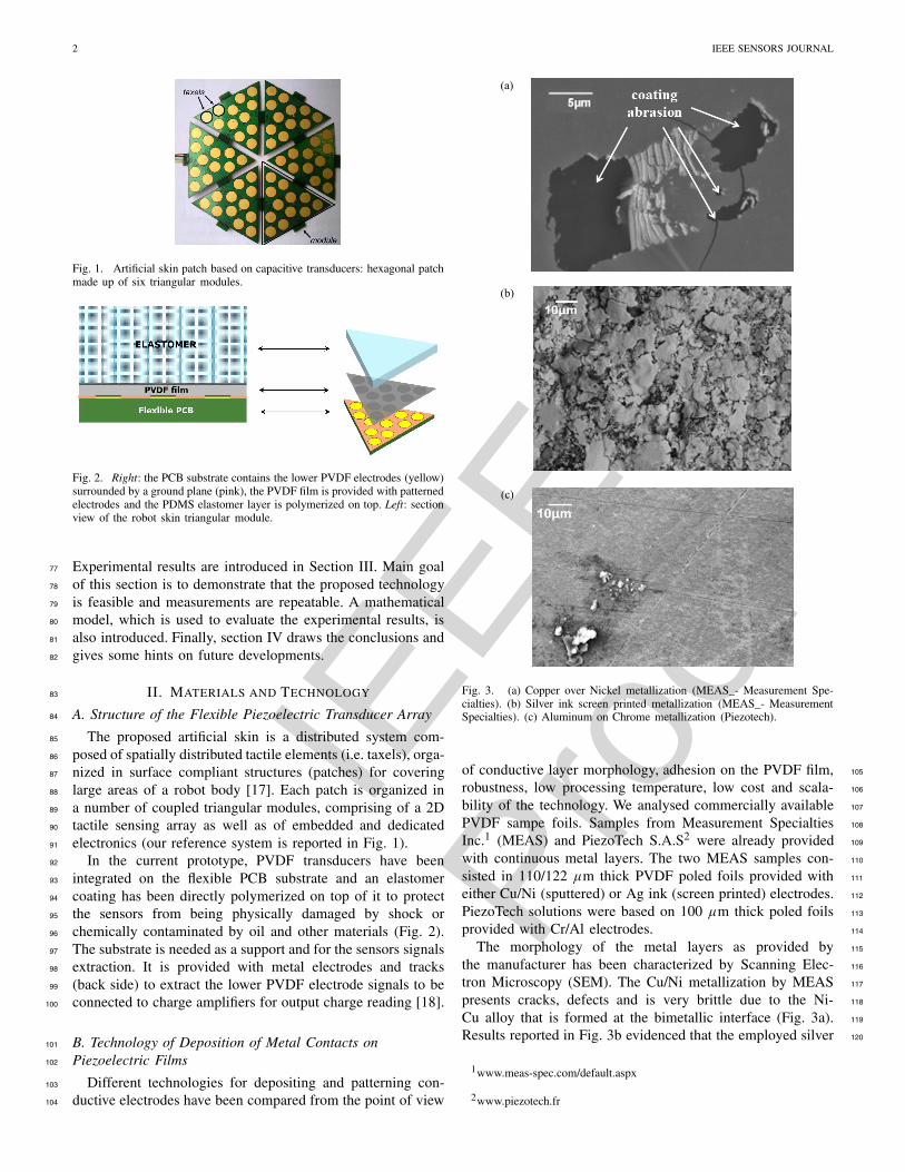
Fig. 1. Artificial skin patch based on capacitive transducers: hexagonal patchmade up of six triangular modules.
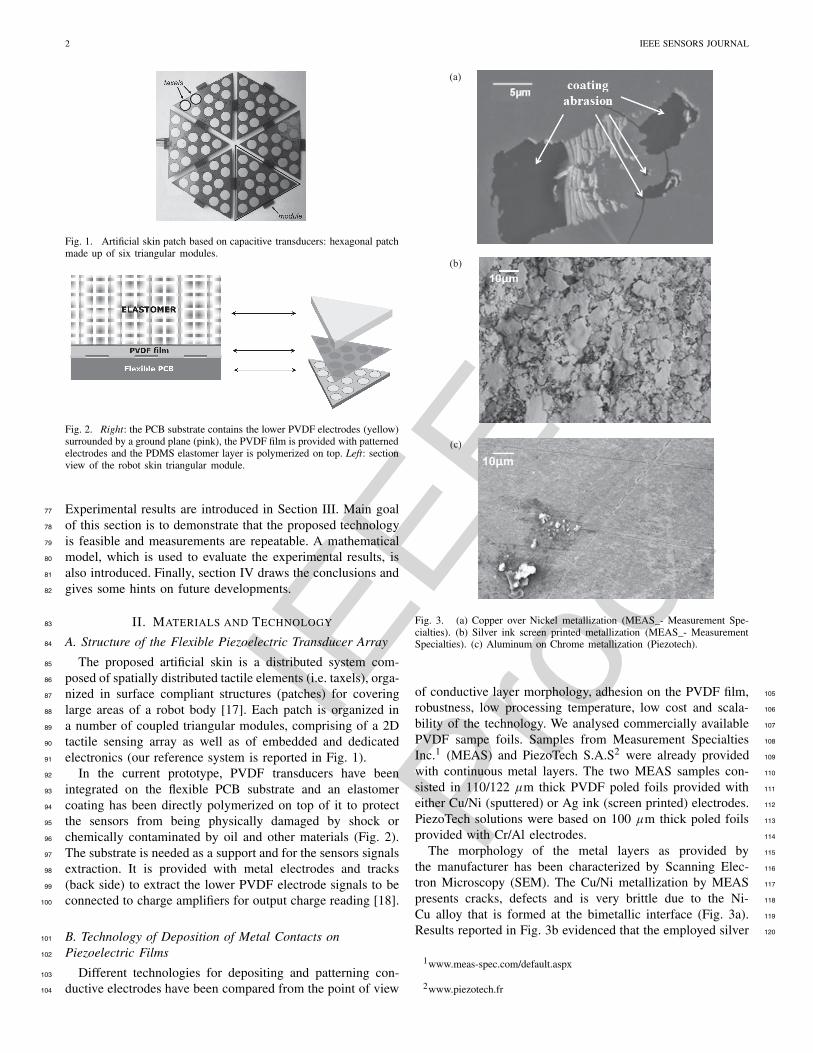
Fig. 2. Right: the PCB substrate contains the lower PVDF electrodes (yellow)surrounded by a ground plane (pink), the PVDF film is provided with patternedelectrodes and the PDMS elastomer layer is polymerized on top. Left: sectionview of the robot skin triangular module.
Experimental results are introduced in Section III. Main goal77
of this section is to demonstrate that the proposed technology78
is feasible and measurements are repeatable. A mathematical79
model, which is used to evaluate the experimental results, is80
also introduced. Finally, section IV draws the conclusions and81
gives some hints on future developments.82
II. MATERIALS AND TECHNOLOGY83
A. Structure of the Flexible Piezoelectric Transducer Array84
The proposed artificial skin is a distributed system com-85
posed of spatially distributed tactile elements (i.e. taxels), orga-86
nized in surface compliant structures (patches) for covering87
large areas of a robot body [17]. Each patch is organized in88
a number of coupled triangular modules, comprising of a 2D89
tactile sensing array as well as of embedded and dedicated90
electronics (our reference system is reported in Fig. 1).91
In the current prototype, PVDF transducers have been92
integrated on the flexible PCB substrate and an elastomer93
coating has been directly polymerized on top of it to protect94
the sensors from being physically damaged by shock or95
chemically contaminated by oil and other materials (Fig. 2).96
The substrate is needed as a support and for the sensors signals97
extraction. It is provided with metal electrodes and tracks98
(back side) to extract the lower PVDF electrode signals to be99
connected to charge amplifiers for output charge reading [18].100
B. Technology of Deposition of Metal Contacts on101
Piezoelectric Films102
Different technologies for depositing and patterning con-103
ductive electrodes have been compared from the point of view104
(a)
(b)
(c)
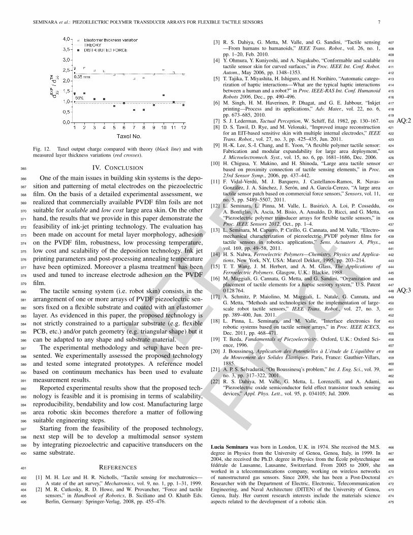
Fig. 3. (a) Copper over Nickel metallization (MEAS_- Measurement Spe-cialties). (b) Silver ink screen printed metallization (MEAS_- MeasurementSpecialties). (c) Aluminum on Chrome metallization (Piezotech).
of conductive layer morphology, adhesion on the PVDF film, 105
robustness, low processing temperature, low cost and scala- 106
bility of the technology. We analysed commercially available 107
PVDF sampe foils. Samples from Measurement Specialties 108
Inc.1 (MEAS) and PiezoTech S.A.S2 were already provided 109
with continuous metal layers. The two MEAS samples con- 110
sisted in 110/122 μm thick PVDF poled foils provided with 111
either Cu/Ni (sputtered) or Ag ink (screen printed) electrodes. 112
PiezoTech solutions were based on 100 μm thick poled foils 113
provided with Cr/Al electrodes. 114
The morphology of the metal layers as provided by 115
the manufacturer has been characterized by Scanning Elec- 116
tron Microscopy (SEM). The Cu/Ni metallization by MEAS 117
presents cracks, defects and is very brittle due to the Ni- 118
Cu alloy that is formed at the bimetallic interface (Fig. 3a). 119
Results reported in Fig. 3b evidenced that the employed silver 120
1www.meas-spec.com/default.aspx
2www.piezotech.fr

IEEE
Proo
f
SEMINARA et al.: PIEZOELECTRIC POLYMER TRANSDUCER ARRAYS FOR FLEXIBLE TACTILE SENSORS 3
flakes present a very poor surface smoothness. Finally, in121
case of the Piezotech samples (Fig. 3c) the metal thin film122
is brittle and presents cracks. The same results have been123
confirmed in different tests, proving the reliability of the124
observations.125
Although metalized PVDF film foils are commercially avail-126
able, the brittleness of some of the available coatings, the high127
roughness of the silver ink solution and the very high cost128
of obtaining custom patterning of the conducting film, make129
these choices not suitable for scalable and low cost large area130
skin.131
Piezoelectric polymer foils without any metallization have132
been used and ad-hoc electrodes realized by employing133
dedicated deposition technologies.134
Different approaches have been considered and tested, con-135
sisting in the deposition and patterning of i) metal layers136
(gold/aluminium) by thermal vapour deposition; ii) gold layers137
by sputtering; iii) conductive polymers by inkjet printing.138
In the first two cases (deposition by thermal vapour deposi-139
tion and sputtering), the deposition takes place inside a High140
Vacuum Chamber (nominal pressure ranging from 5 × 10−5141
to 5 × 10⁻⁶ mbar). The evaporator system is provided with142
a Crystal Quartz Microbalance to control the deposition rate143
and the final film thickness. Gold and aluminium have been144
deposited. The final thickness of the deposited films ranges145
around 50–70 nm.146
Gold electrodes have also been deposited by employing a147
sputter coater, to achieve better adhesion of the deposited metal148
film on the PVDF surface.149
In both cases, the electrodes have been patterned by deposit-150
ing the metal through a shadow mask (1 cm2), the electrodes151
have been deposited on both sides of the PVDF film and152
aligned by an optical microscope.153
SEM images of the electrodes obtained with the above154
described deposition techniques are shown in Fig. 4.155
Among such deposition techniques, most uniform films are156
the sputtered ones. Evaporated gold films have a smaller grain157
size but the coverage is less uniform. However, all these films158
show a resistivity lower than 1 � per square and do appear159
adequate for the application.160
Among these three metal films, the most suitable material161
for the application would be the aluminium coating. However,162
the polymeric nature of the substrate excludes the use of stan-163
dard optical lithography and lift-off techniques for patterning,164
due to the need of compatible solvents such as acetone. A hard165
shadow masking should be needed with all the limitations166
that this implies especially regarding mask alignment during167
evaporation and metal coating shape design.168
We finally evaluated Ink Jet printing for electrode deposition169
and patterning . It allows patterning nearly any shape of metal170
contacts without the need of shadow masks or any other171
lithographic process.172
Commercial bare (no metallized) polarized 110 μm-thick173
PVDF sheets from Measurement Specialties Inc. have been174
purchased. An air plasma treatment (P = 75 W, p = 0.5 Torr,175
t = 60 s) has been used before the printing process to increase176
electrode adhesion to the polymer film, enhancing sensor177
robustness and reliability.178
(a)
(b)
(c)
Fig. 4. (a) Thermal evaporated gold thin film. (b) Thermal evaporated alu-minum thin film. (c) Sputtered gold thin film. Same scale as Fig. 3 (b) and (c).
Metal contacts have been patterned on both sides of PVDF 179
films by means of inkjet printing (Fujifilm Dimatix 2800). 180
For all the metal contacts we used Cabot Conductive Ink 300 181
(CCI-300), a metal ink (provided by Cabot Corporation) made 182
of silver nanoparticles in a liquid vehicle composed of ethanol 183
and ethylene glycol. All details about the printing process are 184
reported in [12]. 185
During printing, PVDF films were kept at 60 °C in order 186
to promote faster solvent evaporation. Two different patterns 187
were printed on the two sides of the substrate: a continuous 188
and homogeneous ink layer (common ground) is deposited 189
on top of the PVDF film. The second pattern was printed on 190
PVDF bottom side, once the first was dried, and consists in 191
12 circles with a diameter of 3 mm each (same geometry of 192
metal contacts on PCB), arranged in a triangular shape. Fig. 5 193
shows both layouts. 194
After deposition, samples have been annealed at 60 °C in 195
an oven for several hours. We observed that annealing at 196
temperatures above 60 °C leads to a huge deformation of the 197
polymer films. 198

IEEE
Proo
f
4 IEEE SENSORS JOURNAL
Fig. 5. Layout of the inkjet printed patterns: circular taxels (left) andcontinuous ground contact (right).
Fig. 6. Inkjet printed colloidal silver film.
SEM pictures after Ag inkjet printing the PVDF samples199
are reported in Fig. 6. Compared to thermal evaporated and200
sputtered films (Fig. 4), inkjet printed electrodes are the most201
uniform among all. The metal surface is shiny and SEM202
images demostrate the very small grain size of the silver203
particles. Combined with the material properties, the computer204
controlled patterning, the scalability and reproducibility of the205
deposition process made inkjet printed colloidal silver the best206
choice for the present application.207
Attention has been paid to test the possible influence of the208
electrode deposition process on the piezoelectric film electro-209
mechanical behaviour. Therefore, the frequency dependent d33210
piezoelectric coefficient [19] has been measured after plasma211
and annealing treatments, to check if some film degradation212
had occurred. Results are reported in Fig. 7 and show that the213
plasma treatment improved the PVDF piezoelectric behavior214
i.e. it increased the d33 value.215
C. Assembly Technology of the Tactile Sensing System216
The basic structure of skin prototypes based on PVDF arrays217
is reported in Fig. 2.218
As reported in Par. II.A, at this prototypal stage wires have219
to be soldered on the PCB back side, to connect PVDF output220
signals to interface electronics. Due to the central (back)221
position of the wire connector and to avoid thermal stress of222
the polymer at a higher temperature than 60 °C, the PCB223
substrate has first been wired. Glue has been used to reinforce224
the soldered wire structure.225
A preliminary procedure with 1 μm parylene deposition226
over PVDF contacts to enhance track robustness has been227
replaced by direct PDMS polymerization. Therefore, the228
PDMS layer is directly integrated on top of the PVDF film.229
A 2.5 mm elastomer thickness has been chosen as optimally230
meeting the application requirements. A Two-part silicone231
Sylgard 184 Silicone Elastomer (Dow Corning) that cures to232
a flexible elastomer (PDMS) has been employed. Sylgard 184233
Silicone Elastomer is supplied as two-part liquid component234
kits comprised of Part A/Part B to be mixed in a 10:1 ratio235
by weight or volume. A suitable quantity is prepared by236
(a)
(b)
Fig. 7. Frequency behavior of the d33 piezoelectric coefficient. (a) Beforeand (b) after plasma and annealing treatments for the PVDF film.
mixing the two components. Care should be taken to minimize 237
air entrapment. To reduce the liquid viscosity (enhancing its 238
capability to level off) a silicone fluid (47V5) has been added 239
at 5% to the liquid solution. The liquid is poured on the 240
PVDF substrate which was previously placed at the bottom 241
of a mold, kept horizontal by means of a level. An adhesion 242
promoter (Dow Corning 1200 OS Primer) has been previously 243
distributed on the PVDF surface to enhance Sylgard adhesion. 244
The mold is finally heat cured for 12 hours at 50 °C, not 245
to depass the PVDF Curie Temperature. Cure is evidenced 246
by a gradual increase in viscosity, followed by gelation and 247
conversion to a PDMS solid elastomer. 248
Patterned PVDF film triangles with elastomer on top were 249
finally glued on the PCB by the use of conductive Epoxy 250
(CW2400, all-spec industries), patterned contacts on the PVDF 251
bottom side corresponding to contacts on the PCB. The 252
optimal amount of conductive glue has been determined by 253
preliminary tests and the coverlay (Fig. 2) is used to avoid 254
short-circuits between taxels and to ensure that the piezoelec- 255
tric film is glued on a plane surface. In order to obtain a 256
constant pressure for the gluing process, 3 kg weight has been 257
placed on top of the PDMS layer. Soldered wires on the PCB 258
back side were kept in place passing through a hole on a 259
suitable support. 260
A completely assembled and ‘ready for testing’ proto- 261
type device is shown in Fig. 8 (a), (b). In Fig. 8 (c) the 262

IEEE
Proo
f
SEMINARA et al.: PIEZOELECTRIC POLYMER TRANSDUCER ARRAYS FOR FLEXIBLE TACTILE SENSORS 5
(a)
(b)
(c)
Fig. 8. (a), (b) Skin module prototype based on piezoelectric polymer arrays.(c) Triangular-shape skin module is adapted to a cylinder of diameter 3.3cmto show its bendability.
triangular-shape skin module is adapted to a cylinder (cur-263
vature radius = 1.65 cm) to show its bendability.264
III. EXPERIMENTAL RESULTS265
The goal of the experimental tests is to validate the proposed266
technology and to assess the performance of the tactile sensing267
system.268
A. Experimental Setup269
The mechanical chain of the experimental setup (Fig. 9) is270
basically constituted by a mechanical shaker (TV 50018, TIRA271
GmbH, Schwingtechnik Vibration Test Systems), the triangu-272
lar skin module (protective layer included) and a load cell273
(Model 208C01, PCB Piezotronics). The inductive mechanical274
actuator that moves the shaker is software controlled. The275
input parameters of the mechanical stimulus (range of fre-276
quencies, amplitude, DC offset) are set and the related signal277
is directly generated by the acquisition board and conveyed278
to the shaker via a conditioner. The charge developed by the279
PVDF film is measured by a charge amplifier [18].280
A 3 mm × 3 mm square indenter has been mounted on the281
shaker to stimulate one taxel at a time.282
Fig. 9. Mechanical setup to characterize the electromechanical behavior ofskin prototypes.
B. Modeling and Test of the Skin Structure 283
A mechanical model of the PVDF tactile sensor with a 284
protective layer on top has been used to test the feasibility and 285
reliability of the proposed system. As a matter of fact, a given 286
charge is expected as output of the transduction of the applied 287
mechanical stimulus, which is conveyed to the PVDF sensor 288
through the elastomer layer. If the measured charge value is in 289
accordance with the one predicted by the model, it means that 290
the mechanical chain of the measurement setup is working as 291
expected and the feasibility of the proposed technology for 292
skin manufacturing is demonstrated. 293
Approximately, the relation between a point load force 294
F applied on the outer surface and the stress at a given 295
point inside the cover layer is given by the Boussinesq’s 296
equation [20]: 297
T = 3
2π
F · er
r2 er ⊗ er (1) 298
where all bold faced symbols represent tensors (T is the stress 299
tensor) or vectors, er is the unit vector in the r -direction and 300
⊗ is the symbol of tensor product. Eq. (1) holds whenever the 301
Poisson ratio ν of the medium is close to 0.5 (this holds for 302
the present elastomer). A complete solution valid for all ν is 303
available [21] but it is considerably more complex. 304
Letting r̂ be the radial distance of the point where the force 305
is applied from the sensor center projected on the outer surface 306
(inset of Fig. 10), for a vertical force F3 (F1 = F2 = 0) 307
(1) allows to retrieve the normal T3 component on the PVDF 308
sensor3: 309
T3 = 3
2π
F3h3
(r̂2 + h2
)5/2. (2) 310
On the other hand, PVDF constitutive equations relate the 311
normal T3 component on the sensor to the output charge 312
density through the d33 piezoelectric modulus (sensor used in 313
thickness mode and electric field E3 across the PVDF sensor 314
assumed to be negligible4) [22] 315
D3 = d33T3. (3) 316
3Eq. (2) is derived from eq. (1) using r2 = r̂2+ h2 and er = sinθ(e1 cosφ+ e2 sinφ) – e3 cosθ , where cosθ = h/r, sinθ = r̂ / r.
4Because of the virtual ground at the operational amplifier inverting input.

IEEE
Proo
f
6 IEEE SENSORS JOURNAL
Fig. 10. Comparison between expected (model from Eq. (4)) and measuredcharge (two different taxels) at frequency of 16 Hz. Error bars related todeviation from the average value are too small to be visible in the plot (<5%).
TABLE I
COMMERCIALLY AVAILABLE METALIZED PVDF FILMS
Manufacturer Film Thickness Electrode Type
PiezoTech S.A.S 100µm Evaporated Cr/Al
Measurement Specialties Inc.
110µm Sputtered Cu/Ni
Screen printed Ag ink 122 µm
Using (2) and (3) and adding the hypotheses that the sensor317
size is sufficiently smaller than its distance from the point318
force, the total charge measured by the PVDF sensor can be319
directly related to the applied F3 load by:320
q = d333A
2π
F3h3
(r̂2 + h2
)5/2(4)321
where A is the area of the PVDF taxel.322
Concentrated sinusoidal force (at fixed frequency equal to323
16 Hz) has been applied on top of the elastomer layer, directly324
above taxels 9 and 12. Output charge has been measured and325
compared with theory. The data points reported in Fig. 10 are326
the average values of peak amplitudes (400 wave periods),
AQ:1
327
both for charge and force. The experimental results show very328
good accordance with what predicted by the model, confirming329
the feasibility of the employed skin manufacturing technology.330
C. Experimental Performance Tests331
Fig. 11a shows the response of a single taxel for four differ-332
ent stimulus frequencies belonging to the range of interest of333
the present application (f = 6, 62, 324, 824 Hz). As it can be334
seen, a linear behaviour is achieved over the whole explored335
range (1 Hz–1 kHz).336
On the other hand, by varying the amplitude of the applied337
stimulus at a fixed frequency (f = 6 Hz), the charge response338
of 5 different taxels belonging to three different triangles can339
be compared (Fig. 11b).340
(a)
(b)
Fig. 11. (a) Response linearity: same taxel, different stimulus frequencies.(b) System reproducibility: charge response of 5 different taxels (f = 6 Hz),placed on three different triangles (Samples 1, 2, 5). Taxel positions areindicated on the triangle on the right.
To better analyse the previous results, an identical triangular 341
prototype but based on a rigid substrate has been manu- 342
factured and tested. The scope is to verify the dependence 343
between the output charge and the thickness of the elastomer 344
layer. 345
In order to better compare the slopes of charge-to-force 346
curves corresponding to slightly different layer thicknesses, 347
thickness values on different taxels have been measured. An 348
average thickness value has been used to evaluate a d33 value 349
through (4), starting from measured charge q and force F3. 350
The dispersion of the ratio between this value and theoretical 351
d33 is directly compared to the dispersion in the values of the 352
point-by-point measured layer thickness. Results reported in 353
Fig. 12 show very good theoretical value reproducibility, as 354
a mean value. On the other hand, the taxel dispersion ouputs 355
results are due to the not uniform thickness of the elastomer 356
layer. Changes as small as 0.35 mm (corresponding to about 357
15% of the layer thickness, typical uncertainty at a prototype 358
stage) reflect in changes of the output charge as high as 50% 359
with respect to the mean value. Better precision in controlling 360
the elastomer layer thickness will be needed if better repro- 361
ducible systems will be targeted. This information becomes a 362
manufacturing process reference specs when moving from a 363
prototype stage to a production engineering step. 364

IEEE
Proo
f
SEMINARA et al.: PIEZOELECTRIC POLYMER TRANSDUCER ARRAYS FOR FLEXIBLE TACTILE SENSORS 7
Fig. 12. Taxel output charge compared with theory (black line) and withmeasured layer thickness variations (red crosses).
IV. CONCLUSION365
One of the main issues in building skin systems is the depo-366
sition and patterning of metal electrodes on the piezoelectric367
film. On the basis of a detailed experimental assessment, we368
realized that commercially available PVDF film foils are not369
suitable for scalable and low cost large area skin. On the other370
hand, the results that we provide in this paper demonstrate the371
feasibility of ink-jet printing technology. The evaluation has372
been made on account for metal layer morphology, adhesion373
on the PVDF film, robustness, low processing temperature,374
low cost and scalability of the deposition technology. Ink jet375
printing parameters and post-processing annealing temperature376
have been optimized. Moreover a plasma treatment has been377
used and tuned to increase electrode adhesion on the PVDF378
film.379
The tactile sensing system (i.e. robot skin) consists in the380
arrangement of one or more arrays of PVDF piezoelectric sen-381
sors fixed on a flexible substrate and coated with an elastomer382
layer. As evidenced in this paper, the proposed technology is383
not strictly constrained to a particular substrate (e.g. flexible384
PCB, etc.) and/or patch geometry (e.g. triangular shape) but it385
can be adapted to any shape and substrate material.386
The experimental methodology and setup have been pre-387
sented. We experimentally assessed the proposed technology388
and tested some integrated prototypes. A reference model389
based on continuum mechanics has been used to evaluate390
measurement results.391
Reported experimental results show that the proposed tech-392
nology is feasible and it is promising in terms of scalability,393
reproducibility, bendability and low cost. Manufacturing large394
area robotic skin becomes therefore a matter of following395
suitable engineering steps.396
Starting from the feasibility of the proposed technology,397
next step will be to develop a multimodal sensor system398
by integrating piezoelectric and capacitive transducers on the399
same substrate.400
REFERENCES401
[1] M. H. Lee and H. R. Nicholls, “Tactile sensing for mechatronics—402
A state of the art survey,” Mechatronics, vol. 9, no. 1, pp. 1–31, 1999.403
[2] M. R. Cutkosky, R. D. Howe, and W. Provancher, “Force and tactile404
sensors,” in Handbook of Robotics, B. Siciliano and O. Khatib Eds.405
Berlin, Germany: Springer-Verlag, 2008, pp. 455–476.406
[3] R. S. Dahiya, G. Metta, M. Valle, and G. Sandini, “Tactile sensing 407
—From humans to humanoids,” IEEE Trans. Robot., vol. 26, no. 1, 408
pp. 1–20, Feb. 2010. 409
[4] Y. Ohmura, Y. Kuniyoshi, and A. Nagakubo, “Conformable and scalable 410
tactile sensor skin for curved surfaces,” in Proc. IEEE Int. Conf. Robot. 411
Autom., May 2006, pp. 1348–1353. 412
[5] T. Tajika, T. Miyashita, H. Ishiguro, and H. Norihiro, “Automatic catego- 413
rization of haptic interactions—What are the typical haptic interactions 414
between a human and a robot?” in Proc. IEEE-RAS Int. Conf. Humanoid 415
Robots 2006, Dec., pp. 490–496. 416
[6] M. Singh, H. M. Haverinen, P. Dhagat, and G. E. Jabbour, “Inkjet 417
printing—Process and its applications,” Adv. Mater., vol. 22, no. 6, 418
pp. 673–685, 2010. 419
[7] S. J. Lederman, Tactual Perception, W. Schiff, Ed. 1982, pp. 130–167. AQ:2420
[8] D. S. Tawil, D. Rye, and M. Velonaki, “Improved image reconstruction 421
for an EIT-based sensitive skin with multiple internal electrodes,” IEEE 422
Trans. Robot., vol. 27, no. 3, pp. 425–435, Jun. 2011. 423
[9] H.-K. Lee, S.-I. Chang, and E. Yoon, “A flexible polymer tactile sensor: 424
Fabrication and modular expandability for large area deployment,” 425
J. Microelectromech. Syst., vol. 15, no. 6, pp. 1681–1686, Dec. 2006. 426
[10] H. Chigusa, Y. Makino, and H. Shinoda, “Large area tactile sensor 427
based on proximity connection of tactile sensing elements,” in Proc. 428
23rd Sensor Symp., 2006, pp. 437–442. 429
[11] F. Vidal-Verdú, M. J. Barquero, J. Castellanos-Ramos, R. Navas- 430
González, J. A. Sánchez, J. Serón, and A. García-Cerezo, “A large area 431
tactile sensor patch based on commercial force sensors,” Sensors, vol. 11, 432
no. 5, pp. 5489–5507, 2011. 433
[12] L. Seminara, L. Pinna, M. Valle, L. Basiricò, A. Loi, P. Cosseddu, 434
A. Bonfiglio, A. Ascia, M. Bisio, A. Ansaldo, D. Ricci, and G. Metta, 435
“Piezoelectric polymer transducer arrays for flexible tactile sensors,” in 436
Proc. IEEE Sensors 2012, Oct., pp. 1–4. 437
[13] L. Seminara, M. Capurro, P. Cirillo, G. Cannata, and M. Valle, “Electro- 438
mechanical characterization of piezoelectric PVDF polymer films for 439
tactile sensors in robotics applications,” Sens. Actuators A, Phys., 440
vol. 169, pp. 49–58, 2011. 441
[14] H. S. Nalwa, Ferroelectric Polymers—Chemistry, Physics and Applica- 442
tions, New York, NY, USA: Marcel Dekker, 1995, pp. 203–214. 443
[15] T. T. Wang, J. M. Herbert, and A. M. Glass, The Applications of 444
Ferroelectric Polymers. Glasgow, U.K.: Blackie, 1988. 445
[16] M. Maggiali, G. Cannata, G. Metta, and G. Sandini, “Organization and 446
placement of tactile elements for a haptic sensory system,” U.S. Patent 447
0 128 764. AQ:3448
[17] A. Schmitz, P. Maiolino, M. Maggiali, L. Natale, G. Cannata, and 449
G. Metta, “Methods and technologies for the implementation of large- 450
scale robot tactile sensors,” IEEE Trans. Robot., vol. 27, no. 3, 451
pp. 389–400, Jun. 2011. 452
[18] L. Pinna, L. Seminara, and M. Valle, “Interface electronics for 453
robotic systems based on tactile sensor arrays,” in Proc. IEEE ICECS, 454
Dec. 2011, pp. 468–471. 455
[19] T. Ikeda, Fundamentals of Piezoelectricity. Oxford, U.K.: Oxford Sci- 456
ence, 1996. 457
[20] J. Boussinesq, Application des Potentielles à L’étude de L’équilibre et 458
du Mouvement des Solides Élastiques. Paris, France: Gauthier-Villars, 459
1885. 460
[21] A. P. S. Selvadurai, “On Boussinesq’s problem,” Int. J. Eng. Sci., vol. 39, 461
no. 3, pp. 317–322, 2001. 462
[22] R. S. Dahiya, M. Valle, G. Metta, L. Lorenzelli, and A. Adami, 463
“Piezoelectric oxide semiconductor field effect transistor touch sensing 464
devices,” Appl. Phys. Lett., vol. 95, p. 034105; Jul. 2009. 465
Lucia Seminara was born in London, U.K. in 1974. She received the M.S. 466
degree in Physics from the University of Genoa, Genoa, Italy, in 1999. In 467
2004, she received the Ph.D. degree in Physics from the École polytechnique 468
fédérale de Lausanne, Lausanne, Switzerland. From 2005 to 2009, she 469
worked in a telecommunications company, working on wireless networks 470
of nanostructured gas sensors. Since 2009, she has been a Post-Doctoral 471
Researcher with the Department of Electric, Electronic, Telecommunication 472
Engineering, and Naval Architecture (DITEN) of the University of Genoa, 473
Genoa, Italy. Her current research interests include the materials science 474
aspects related to the development of a robotic skin. 475

IEEE
Proo
f
8 IEEE SENSORS JOURNAL
Luigi Pinna was born in Cagliari, Italy, in 1978. He received the M.Sc. degree476
in electronic engineering from the University of Cagliari, Cagliari, Italy, in477
2005 and the Ph.D. degree in nanotechnologies from the University of Genoa,478
in 2010. Since 2010, he has been with the Department of Electric, Electronic,479
Telecommunication Engineering, and Naval Architecture (DITEN), University480
of Genoa. His current research interests include based-charge amplifiers circuit481
design for PVDF tactile sensor arrays, Organic Thin Film Transistors (OTFT)-482
based, and POSFET (Piezoelectric-Oxide-FET)-based tactile sensing arrays483
for humanoid robots.484
Maurizio Valle received the M.S. degree in Electronic Engineering in 1985485
and the Ph.D. degree in Electronic and Computer Science Engineering from486
the University of Genova, Italy, in 1990. From 1992 to 2006, he was an487
Assistant Professor. Since January 2007, he has been an Associate Professor488
in Electronic Engineering with the Department of Electrical, Electronic,489
Telecommunication Engineering, and Naval Architecture (DITEN), University490
of Genova. Dr. Valle is co-author of more than 180 articles on international491
scientific journals and conference proceedings. His current research interests492
include tactile sensors and systems, microelectronic embedded systems, and493
wireless sensor networks. He is member of IEEE.494
Laura Basiricò received the M.S. degree in Physics from the University495
of Bologna, Bologna, Italy, in 2008. In 2009, she joined the University496
of Cagliari with the Department of Electrical and Electronic Engineering497
as the Ph.D student. She received the Ph.D. degree in 2012. During the498
Ph.D. degree, she focused her research activity on the development of inkjet499
printing technique for the realization of Organic Field Effect Transistors500
and Organic ElectroChemical Transistors for the sensing application. She501
is currently a Researcher with ISMN-CNR, Bologna. Her current research502
interests include the field of organic electronic devices on the fabrication and503
physical characterization of Organic Field Effect Transistors for light emission504
and sensing applications.505
Alberto Loi received the Master Degree in Electronic Engineering from the506
University of Bologna, Italy, in 2010, discussing the thesis “Analysis of a507
30-V multifinger LDMOS power device.” In 2011, he joined the DEALAB508
group with the University of Cagliari, where he worked as the Ph.D. student.509
His current research interests include inkjet printing of organic materials,510
fabrication and characterization of Organic Field Effect Transistors, and511
fabrication and characterization of mechanical sensors and sensing systems512
based on organic devices.513
Piero Cosseddu graduated in Electronic Engineering, in 2003, and received514
the Ph.D. degree in Electronic and Computer Science Engineering in 2007515
from the University of Cagliari, Italy. Since May 2007, he has been a Post-516
Doctoral Fellow with the Department of Electrical and Electronic Engineering,517
University of Cagliari. His current research interests include the design,518
realization, and characterization of organic semiconductor-based devices for519
innovative applications such as artificial electronic skin, biomedical sensing,520
and wearable electronics.521
Annalisa Bonfiglio received the Laurea Degree in Physics from the University522
of Genoa, in 1991 and the Ph.D. degree in Bioengineering from the Politecnico523
di Milano, Milano, Italy, in 1995. She is currently an Associate Professor524
of Electronics and Electronic Bioengineering with the University of Cagliari,525
Italy. She is also a member of the Institute of Nanoscience- National Research526
Council. She is an author of more than 130 papers on international journals,527
conference proceedings, book chapters, and five patents. Her current research528
interests include innovative materials and electronic devices for wearable529
electronics and bioengineering and several international and national research530
Projects.531
Alberto Ascia received the master’s degree in Computer Science Engineering 532
and the Ph.D. degree in “Electronic Engineering, Automation and Control of 533
Complex Systems” from the University of Catania, Catania, Italy, in 2005 534
and 2009, respectively. During the Ph.D. degree, he focused on design and 535
characterization of transducers based on magnetic fluids. From January 2010 536
to July 2012, he has been a Post-Doctoral Researcher with the Istituto Italiano 537
di Tecnologia. Her current research interests include novel technologies for 538
the design and characterization of artificial skin for the iCub humanoid robot. 539
He is currently an Instrumentation Test Engineer with an aeronautic company. 540
Maurizio Biso received the M.Sc. degree in Industrial Chemistry and the 541
Ph.D. degree in Robotics, Neuroscience, and Nanotechnology. He is currently 542
a Postdoc with the Robotics, Brain, and Cognitive Sciences Department, 543
Istituto Italiano di Tecnologia, Genoa, Italy mainly working on composite 544
materials based on carbon nanotubes for robotics. His current research 545
interests include the development of “soft” materials for sensors and actu- 546
ators. He has a strong experience in electrochemistry and in synthesis and 547
characterization of polymeric materials. 548
Alberto Ansaldo received the M.Sc. degree in Electronic Engineering and 549
the Ph.D. degree in Communication Science and Technology, Genoa, Italy. 550
He is mainly working on Chemical Vapour Deposition of Carbon Nanotubes 551
for Electronic Applications. He is currently Research Technologist with the 552
Robotics Brain and Cognitive Science Department of the Italian Institute of 553
Technology, Genoa, Italy, in the Soft Materials Design Laboratory. His current 554
research interests include nanoscience, robotics, and bioengineering, with a 555
focus on the development of technologies based on novel materials such as 556
conductive polymers and carbon nanomaterials. 557
Davide Ricci received the M.Sc. degree in Physics and the Ph.D. degree 558
in Electronic Engineering and Computer Science from the University of 559
Genoa, Genoa, Italy, in 1989 and 1993, respectively. He is currently a Team 560
Leader with the Robotics Brain and Cognitive Science Department, Italian 561
Institute of Technology, Genoa, Italy. His current research interests include 562
the development of devices such as neural electrodes for Brain Machine 563
Interfaces, of flexible nano-actuators and sensors for robotics and of smart 564
interfaces for tissue engineering and prosthetics. He has co-authored more 565
than 100 papers on such topics. 566
Giorgio Metta is the Director of the iCub Facility department with the Istituto 567
Italiano di Tecnologia (IIT), Genoa, Italy, where he coordinates the iCub 568
project. He received the M.Sc. degree cum laude, in 1994, and the Ph.D. 569
degree, in 2000, in electronic engineering from the University of Genoa. 570
In 2001 and 2002, he has been a Post-Doctoral Associate with the MIT 571
AI-Lab. Since 2012, he has been the Professor of Cognitive Robotics with 572
the University of Plymouth, Plymouth, U.K. His current research interests 573
include the fields of biologically motivated and humanoid robotics and 574
developing robots that can adapt and learn from experience. He is an author 575
of approximately 200 scientific publications. 576

IEEE
Proo
f
AUTHOR QUERIES
AQ:1 = Table I is not cited in the body text. Please indicate where it should be cited.AQ:2 = Please provide the publisher name and location for ref. [7].AQ:3 = Please provide the date, month, and year for ref. [16].

IEEE
Proo
f
IEEE SENSORS JOURNAL 1
Piezoelectric Polymer Transducer Arraysfor Flexible Tactile Sensors
Lucia Seminara, Luigi Pinna, Maurizio Valle, Member, IEEE, Laura Basiricò, Alberto Loi, Piero Cosseddu,Annalisa Bonfiglio, Alberto Ascia, Maurizio Biso, Alberto Ansaldo, Davide Ricci, and Giorgio Metta
Abstract— In this paper, we propose a novel technological1
approach for the implementation of large-area flexible artificial2
skin based on arrays of piezoelectric polymer transducers.3
Polyvinylidene fluoride (PVDF) transducers are chosen for the4
high electromechanical transduction frequency bandwidth (up to5
1 kHz). A low-cost and scalable technique for extracting PVDF6
signals is used to directly provide the piezoelectric film with7
patterned electrodes. If the skin is meant to cover large areas8
of a robot body, specific requirements have to be fulfilled from9
the point of view of the overall system and of the technology.10
Experimental tests on the prototype skin modules demonstrate11
the feasibility of the proposed approach and reveal the potential-12
ity to build large area flexible skin.13
Index Terms— PVDF piezoelectric transducers, artificial skin,14
flexible sensors, ink jet printing, materials processing, robotic15
skin.16
I. INTRODUCTION17
AWIDE number of tactile sensors and systems have been18
proposed over the last two decades and more [1]–[5].19
To effectively use artificial skin on robots (and not only), it20
has been evidenced that the overall skin performance depends21
not only on the characteristics of individual elements but22
also on the system strategy to integrate the large number23
of components/arrays and to cover large areas of the robot24
body. Therefore, relevant technological issues must be faced25
based on a system perspective. One of the main issues in26
building skin systems is the deposition and patterning of27
metal electrodes on the sensing film. Inkjet printing has been28
chosen and it is proposed to deposit patterned metal layers29
on the sensing film. The appeal of this technology lies in30
Manuscript received April 27, 2013; accepted June 3, 2013. This work wassupported in part by the European project “ROBOSKIN” about Skin-BasedTechnologies and Capabilities for Safe, Autonomous and Interactive Robotsunder Grant 231500. The associate editor coordinating the review of this paperand approving it for publication was Dr. Ravinder S. Dahiya.
L. Seminara, L. Pinna, and M. Valle are with the Department ofTelecommunications, Electronic, Electric and Naval Engineering, Univer-sity of Genoa, Genoa 65000-65480, Italy (e-mail: [email protected];[email protected]; [email protected]).
L. Basiricò, A. Loi, P. Cosseddu, and A. Bonfiglio are with the Departmentof Electrical and Electronic Engineering, University of Cagliari, Cagliari09123, Italy (e-mail: [email protected]; [email protected];[email protected]; [email protected]).
A. Ascia, M. Biso, A. Ansaldo, D. Ricci, and G. Metta are with the Depart-ment of Robotics, Brain and Cognitive Sciences, Istituto Italiano di Tecnolo-gia, Genoa 16163, Italy (e-mail: [email protected]; [email protected];[email protected]; [email protected]; [email protected]).
Color versions of one or more of the figures in this paper are availableonline at http://ieeexplore.ieee.org.
Digital Object Identifier 10.1109/JSEN.2013.2268690
its scalability to large area manufacturing through a maskless 31
approach [6]. 32
If the aim is to mimic the behavior of the human skin, 33
different transducers have to be integrated, to cover the 34
0–1 kHz range of the stimulus frequencies required for 35
the application [7]. In this perspective, our research activity 36
focuses mainly on two different transducers, piezoelectric and 37
capacitive, studying methods and technologies enabling their 38
implementation on available robotic platforms. In this paper, 39
we address the study on piezoelectric polymer transducers 40
concentrating on the use of flexible films of polyvinylidene 41
fluoride (PVDF) to realize scalable, bendable and low-cost 42
sensing systems for large area skin [8]–[12]. 43
We choose PVDF as sensing material because in principle 44
it allows for the direct measurement of the mechanical stress, 45
decoupling tensile and shear stress components (according 46
to the way it is integrated in the artificial skin). In this 47
context, we focus on the T33 normal stress measurement 48
(through thickness direction) [13]. Other advantages of PVDF 49
are the large electro-mechanical transduction frequency band- 50
width (i.e. from few Hz up to 1kHz), the wide measurement 51
range, high elastic compliance/piezoelectricity/permittivity, 52
low weight and low cost [14], [15]. 53
The piezoelectric film has to be integrated in a flexi- 54
ble/conformable skin structure which requires tackling various 55
technological issues in order to make the process feasible, 56
controllable and scalable. In the perspective of system integra- 57
tion with capacitive transducers, triangular patches [16] have 58
been realized which can be organized in flexible structures 59
to adequately cover curved and large surfaces of a robot 60
body. However, the technology presented in this paper is not 61
constrained to the particular triangular substrate and patch 62
geometry. 63
To our knowledge, no paper addresses the exhaustive 64
electromechanical characterization of tactile sensing systems 65
based on piezoelectric PVDF polymers, also due to the diffi- 66
culty in making the whole manufacturing process controllable 67
and reproducible. Efforts have been made towards this direc- 68
tion and the results will be presented in this paper. 69
This paper is organized as follows. Section II introduces 70
the structure of the flexible piezoelectric transducer array, the 71
deposition technology of metal contacts on piezoelectric films 72
(which is one of the main contributions of this paper) and 73
the assembly technology. This section basically introduces 74
main technological solutions for developing reliable flexible 75
tactile sensor arrays based on PVDF piezoelectric polymers. 76
1530-437X/$31.00 © 2013 IEEE
IEEE
Proo
f
2 IEEE SENSORS JOURNAL
Fig. 1. Artificial skin patch based on capacitive transducers: hexagonal patchmade up of six triangular modules.
Fig. 2. Right: the PCB substrate contains the lower PVDF electrodes (yellow)surrounded by a ground plane (pink), the PVDF film is provided with patternedelectrodes and the PDMS elastomer layer is polymerized on top. Left: sectionview of the robot skin triangular module.
Experimental results are introduced in Section III. Main goal77
of this section is to demonstrate that the proposed technology78
is feasible and measurements are repeatable. A mathematical79
model, which is used to evaluate the experimental results, is80
also introduced. Finally, section IV draws the conclusions and81
gives some hints on future developments.82
II. MATERIALS AND TECHNOLOGY83
A. Structure of the Flexible Piezoelectric Transducer Array84
The proposed artificial skin is a distributed system com-85
posed of spatially distributed tactile elements (i.e. taxels), orga-86
nized in surface compliant structures (patches) for covering87
large areas of a robot body [17]. Each patch is organized in88
a number of coupled triangular modules, comprising of a 2D89
tactile sensing array as well as of embedded and dedicated90
electronics (our reference system is reported in Fig. 1).91
In the current prototype, PVDF transducers have been92
integrated on the flexible PCB substrate and an elastomer93
coating has been directly polymerized on top of it to protect94
the sensors from being physically damaged by shock or95
chemically contaminated by oil and other materials (Fig. 2).96
The substrate is needed as a support and for the sensors signals97
extraction. It is provided with metal electrodes and tracks98
(back side) to extract the lower PVDF electrode signals to be99
connected to charge amplifiers for output charge reading [18].100
B. Technology of Deposition of Metal Contacts on101
Piezoelectric Films102
Different technologies for depositing and patterning con-103
ductive electrodes have been compared from the point of view104
(a)
(b)
(c)
Fig. 3. (a) Copper over Nickel metallization (MEAS_- Measurement Spe-cialties). (b) Silver ink screen printed metallization (MEAS_- MeasurementSpecialties). (c) Aluminum on Chrome metallization (Piezotech).
of conductive layer morphology, adhesion on the PVDF film, 105
robustness, low processing temperature, low cost and scala- 106
bility of the technology. We analysed commercially available 107
PVDF sampe foils. Samples from Measurement Specialties 108
Inc.1 (MEAS) and PiezoTech S.A.S2 were already provided 109
with continuous metal layers. The two MEAS samples con- 110
sisted in 110/122 μm thick PVDF poled foils provided with 111
either Cu/Ni (sputtered) or Ag ink (screen printed) electrodes. 112
PiezoTech solutions were based on 100 μm thick poled foils 113
provided with Cr/Al electrodes. 114
The morphology of the metal layers as provided by 115
the manufacturer has been characterized by Scanning Elec- 116
tron Microscopy (SEM). The Cu/Ni metallization by MEAS 117
presents cracks, defects and is very brittle due to the Ni- 118
Cu alloy that is formed at the bimetallic interface (Fig. 3a). 119
Results reported in Fig. 3b evidenced that the employed silver 120
1www.meas-spec.com/default.aspx
2www.piezotech.fr

IEEE
Proo
f
SEMINARA et al.: PIEZOELECTRIC POLYMER TRANSDUCER ARRAYS FOR FLEXIBLE TACTILE SENSORS 3
flakes present a very poor surface smoothness. Finally, in121
case of the Piezotech samples (Fig. 3c) the metal thin film122
is brittle and presents cracks. The same results have been123
confirmed in different tests, proving the reliability of the124
observations.125
Although metalized PVDF film foils are commercially avail-126
able, the brittleness of some of the available coatings, the high127
roughness of the silver ink solution and the very high cost128
of obtaining custom patterning of the conducting film, make129
these choices not suitable for scalable and low cost large area130
skin.131
Piezoelectric polymer foils without any metallization have132
been used and ad-hoc electrodes realized by employing133
dedicated deposition technologies.134
Different approaches have been considered and tested, con-135
sisting in the deposition and patterning of i) metal layers136
(gold/aluminium) by thermal vapour deposition; ii) gold layers137
by sputtering; iii) conductive polymers by inkjet printing.138
In the first two cases (deposition by thermal vapour deposi-139
tion and sputtering), the deposition takes place inside a High140
Vacuum Chamber (nominal pressure ranging from 5 × 10−5141
to 5 × 10⁻⁶ mbar). The evaporator system is provided with142
a Crystal Quartz Microbalance to control the deposition rate143
and the final film thickness. Gold and aluminium have been144
deposited. The final thickness of the deposited films ranges145
around 50–70 nm.146
Gold electrodes have also been deposited by employing a147
sputter coater, to achieve better adhesion of the deposited metal148
film on the PVDF surface.149
In both cases, the electrodes have been patterned by deposit-150
ing the metal through a shadow mask (1 cm2), the electrodes151
have been deposited on both sides of the PVDF film and152
aligned by an optical microscope.153
SEM images of the electrodes obtained with the above154
described deposition techniques are shown in Fig. 4.155
Among such deposition techniques, most uniform films are156
the sputtered ones. Evaporated gold films have a smaller grain157
size but the coverage is less uniform. However, all these films158
show a resistivity lower than 1 � per square and do appear159
adequate for the application.160
Among these three metal films, the most suitable material161
for the application would be the aluminium coating. However,162
the polymeric nature of the substrate excludes the use of stan-163
dard optical lithography and lift-off techniques for patterning,164
due to the need of compatible solvents such as acetone. A hard165
shadow masking should be needed with all the limitations166
that this implies especially regarding mask alignment during167
evaporation and metal coating shape design.168
We finally evaluated Ink Jet printing for electrode deposition169
and patterning . It allows patterning nearly any shape of metal170
contacts without the need of shadow masks or any other171
lithographic process.172
Commercial bare (no metallized) polarized 110 μm-thick173
PVDF sheets from Measurement Specialties Inc. have been174
purchased. An air plasma treatment (P = 75 W, p = 0.5 Torr,175
t = 60 s) has been used before the printing process to increase176
electrode adhesion to the polymer film, enhancing sensor177
robustness and reliability.178
(a)
(b)
(c)
Fig. 4. (a) Thermal evaporated gold thin film. (b) Thermal evaporated alu-minum thin film. (c) Sputtered gold thin film. Same scale as Fig. 3 (b) and (c).
Metal contacts have been patterned on both sides of PVDF 179
films by means of inkjet printing (Fujifilm Dimatix 2800). 180
For all the metal contacts we used Cabot Conductive Ink 300 181
(CCI-300), a metal ink (provided by Cabot Corporation) made 182
of silver nanoparticles in a liquid vehicle composed of ethanol 183
and ethylene glycol. All details about the printing process are 184
reported in [12]. 185
During printing, PVDF films were kept at 60 °C in order 186
to promote faster solvent evaporation. Two different patterns 187
were printed on the two sides of the substrate: a continuous 188
and homogeneous ink layer (common ground) is deposited 189
on top of the PVDF film. The second pattern was printed on 190
PVDF bottom side, once the first was dried, and consists in 191
12 circles with a diameter of 3 mm each (same geometry of 192
metal contacts on PCB), arranged in a triangular shape. Fig. 5 193
shows both layouts. 194
After deposition, samples have been annealed at 60 °C in 195
an oven for several hours. We observed that annealing at 196
temperatures above 60 °C leads to a huge deformation of the 197
polymer films. 198

IEEE
Proo
f
4 IEEE SENSORS JOURNAL
Fig. 5. Layout of the inkjet printed patterns: circular taxels (left) andcontinuous ground contact (right).
Fig. 6. Inkjet printed colloidal silver film.
SEM pictures after Ag inkjet printing the PVDF samples199
are reported in Fig. 6. Compared to thermal evaporated and200
sputtered films (Fig. 4), inkjet printed electrodes are the most201
uniform among all. The metal surface is shiny and SEM202
images demostrate the very small grain size of the silver203
particles. Combined with the material properties, the computer204
controlled patterning, the scalability and reproducibility of the205
deposition process made inkjet printed colloidal silver the best206
choice for the present application.207
Attention has been paid to test the possible influence of the208
electrode deposition process on the piezoelectric film electro-209
mechanical behaviour. Therefore, the frequency dependent d33210
piezoelectric coefficient [19] has been measured after plasma211
and annealing treatments, to check if some film degradation212
had occurred. Results are reported in Fig. 7 and show that the213
plasma treatment improved the PVDF piezoelectric behavior214
i.e. it increased the d33 value.215
C. Assembly Technology of the Tactile Sensing System216
The basic structure of skin prototypes based on PVDF arrays217
is reported in Fig. 2.218
As reported in Par. II.A, at this prototypal stage wires have219
to be soldered on the PCB back side, to connect PVDF output220
signals to interface electronics. Due to the central (back)221
position of the wire connector and to avoid thermal stress of222
the polymer at a higher temperature than 60 °C, the PCB223
substrate has first been wired. Glue has been used to reinforce224
the soldered wire structure.225
A preliminary procedure with 1 μm parylene deposition226
over PVDF contacts to enhance track robustness has been227
replaced by direct PDMS polymerization. Therefore, the228
PDMS layer is directly integrated on top of the PVDF film.229
A 2.5 mm elastomer thickness has been chosen as optimally230
meeting the application requirements. A Two-part silicone231
Sylgard 184 Silicone Elastomer (Dow Corning) that cures to232
a flexible elastomer (PDMS) has been employed. Sylgard 184233
Silicone Elastomer is supplied as two-part liquid component234
kits comprised of Part A/Part B to be mixed in a 10:1 ratio235
by weight or volume. A suitable quantity is prepared by236
(a)
(b)
Fig. 7. Frequency behavior of the d33 piezoelectric coefficient. (a) Beforeand (b) after plasma and annealing treatments for the PVDF film.
mixing the two components. Care should be taken to minimize 237
air entrapment. To reduce the liquid viscosity (enhancing its 238
capability to level off) a silicone fluid (47V5) has been added 239
at 5% to the liquid solution. The liquid is poured on the 240
PVDF substrate which was previously placed at the bottom 241
of a mold, kept horizontal by means of a level. An adhesion 242
promoter (Dow Corning 1200 OS Primer) has been previously 243
distributed on the PVDF surface to enhance Sylgard adhesion. 244
The mold is finally heat cured for 12 hours at 50 °C, not 245
to depass the PVDF Curie Temperature. Cure is evidenced 246
by a gradual increase in viscosity, followed by gelation and 247
conversion to a PDMS solid elastomer. 248
Patterned PVDF film triangles with elastomer on top were 249
finally glued on the PCB by the use of conductive Epoxy 250
(CW2400, all-spec industries), patterned contacts on the PVDF 251
bottom side corresponding to contacts on the PCB. The 252
optimal amount of conductive glue has been determined by 253
preliminary tests and the coverlay (Fig. 2) is used to avoid 254
short-circuits between taxels and to ensure that the piezoelec- 255
tric film is glued on a plane surface. In order to obtain a 256
constant pressure for the gluing process, 3 kg weight has been 257
placed on top of the PDMS layer. Soldered wires on the PCB 258
back side were kept in place passing through a hole on a 259
suitable support. 260
A completely assembled and ‘ready for testing’ proto- 261
type device is shown in Fig. 8 (a), (b). In Fig. 8 (c) the 262

IEEE
Proo
f
SEMINARA et al.: PIEZOELECTRIC POLYMER TRANSDUCER ARRAYS FOR FLEXIBLE TACTILE SENSORS 5
(a)
(b)
(c)
Fig. 8. (a), (b) Skin module prototype based on piezoelectric polymer arrays.(c) Triangular-shape skin module is adapted to a cylinder of diameter 3.3cmto show its bendability.
triangular-shape skin module is adapted to a cylinder (cur-263
vature radius = 1.65 cm) to show its bendability.264
III. EXPERIMENTAL RESULTS265
The goal of the experimental tests is to validate the proposed266
technology and to assess the performance of the tactile sensing267
system.268
A. Experimental Setup269
The mechanical chain of the experimental setup (Fig. 9) is270
basically constituted by a mechanical shaker (TV 50018, TIRA271
GmbH, Schwingtechnik Vibration Test Systems), the triangu-272
lar skin module (protective layer included) and a load cell273
(Model 208C01, PCB Piezotronics). The inductive mechanical274
actuator that moves the shaker is software controlled. The275
input parameters of the mechanical stimulus (range of fre-276
quencies, amplitude, DC offset) are set and the related signal277
is directly generated by the acquisition board and conveyed278
to the shaker via a conditioner. The charge developed by the279
PVDF film is measured by a charge amplifier [18].280
A 3 mm × 3 mm square indenter has been mounted on the281
shaker to stimulate one taxel at a time.282
Fig. 9. Mechanical setup to characterize the electromechanical behavior ofskin prototypes.
B. Modeling and Test of the Skin Structure 283
A mechanical model of the PVDF tactile sensor with a 284
protective layer on top has been used to test the feasibility and 285
reliability of the proposed system. As a matter of fact, a given 286
charge is expected as output of the transduction of the applied 287
mechanical stimulus, which is conveyed to the PVDF sensor 288
through the elastomer layer. If the measured charge value is in 289
accordance with the one predicted by the model, it means that 290
the mechanical chain of the measurement setup is working as 291
expected and the feasibility of the proposed technology for 292
skin manufacturing is demonstrated. 293
Approximately, the relation between a point load force 294
F applied on the outer surface and the stress at a given 295
point inside the cover layer is given by the Boussinesq’s 296
equation [20]: 297
T = 3
2π
F · er
r2 er ⊗ er (1) 298
where all bold faced symbols represent tensors (T is the stress 299
tensor) or vectors, er is the unit vector in the r -direction and 300
⊗ is the symbol of tensor product. Eq. (1) holds whenever the 301
Poisson ratio ν of the medium is close to 0.5 (this holds for 302
the present elastomer). A complete solution valid for all ν is 303
available [21] but it is considerably more complex. 304
Letting r̂ be the radial distance of the point where the force 305
is applied from the sensor center projected on the outer surface 306
(inset of Fig. 10), for a vertical force F3 (F1 = F2 = 0) 307
(1) allows to retrieve the normal T3 component on the PVDF 308
sensor3: 309
T3 = 3
2π
F3h3
(r̂2 + h2
)5/2. (2) 310
On the other hand, PVDF constitutive equations relate the 311
normal T3 component on the sensor to the output charge 312
density through the d33 piezoelectric modulus (sensor used in 313
thickness mode and electric field E3 across the PVDF sensor 314
assumed to be negligible4) [22] 315
D3 = d33T3. (3) 316
3Eq. (2) is derived from eq. (1) using r2 = r̂2+ h2 and er = sinθ(e1 cosφ+ e2 sinφ) – e3 cosθ , where cosθ = h/r, sinθ = r̂ / r.
4Because of the virtual ground at the operational amplifier inverting input.

IEEE
Proo
f
6 IEEE SENSORS JOURNAL
Fig. 10. Comparison between expected (model from Eq. (4)) and measuredcharge (two different taxels) at frequency of 16 Hz. Error bars related todeviation from the average value are too small to be visible in the plot (<5%).
TABLE I
COMMERCIALLY AVAILABLE METALIZED PVDF FILMS
Manufacturer Film Thickness Electrode Type
PiezoTech S.A.S 100µm Evaporated Cr/Al
Measurement Specialties Inc.
110µm Sputtered Cu/Ni
Screen printed Ag ink 122 µm
Using (2) and (3) and adding the hypotheses that the sensor317
size is sufficiently smaller than its distance from the point318
force, the total charge measured by the PVDF sensor can be319
directly related to the applied F3 load by:320
q = d333A
2π
F3h3
(r̂2 + h2
)5/2(4)321
where A is the area of the PVDF taxel.322
Concentrated sinusoidal force (at fixed frequency equal to323
16 Hz) has been applied on top of the elastomer layer, directly324
above taxels 9 and 12. Output charge has been measured and325
compared with theory. The data points reported in Fig. 10 are326
the average values of peak amplitudes (400 wave periods),
AQ:1
327
both for charge and force. The experimental results show very328
good accordance with what predicted by the model, confirming329
the feasibility of the employed skin manufacturing technology.330
C. Experimental Performance Tests331
Fig. 11a shows the response of a single taxel for four differ-332
ent stimulus frequencies belonging to the range of interest of333
the present application (f = 6, 62, 324, 824 Hz). As it can be334
seen, a linear behaviour is achieved over the whole explored335
range (1 Hz–1 kHz).336
On the other hand, by varying the amplitude of the applied337
stimulus at a fixed frequency (f = 6 Hz), the charge response338
of 5 different taxels belonging to three different triangles can339
be compared (Fig. 11b).340
(a)
(b)
Fig. 11. (a) Response linearity: same taxel, different stimulus frequencies.(b) System reproducibility: charge response of 5 different taxels (f = 6 Hz),placed on three different triangles (Samples 1, 2, 5). Taxel positions areindicated on the triangle on the right.
To better analyse the previous results, an identical triangular 341
prototype but based on a rigid substrate has been manu- 342
factured and tested. The scope is to verify the dependence 343
between the output charge and the thickness of the elastomer 344
layer. 345
In order to better compare the slopes of charge-to-force 346
curves corresponding to slightly different layer thicknesses, 347
thickness values on different taxels have been measured. An 348
average thickness value has been used to evaluate a d33 value 349
through (4), starting from measured charge q and force F3. 350
The dispersion of the ratio between this value and theoretical 351
d33 is directly compared to the dispersion in the values of the 352
point-by-point measured layer thickness. Results reported in 353
Fig. 12 show very good theoretical value reproducibility, as 354
a mean value. On the other hand, the taxel dispersion ouputs 355
results are due to the not uniform thickness of the elastomer 356
layer. Changes as small as 0.35 mm (corresponding to about 357
15% of the layer thickness, typical uncertainty at a prototype 358
stage) reflect in changes of the output charge as high as 50% 359
with respect to the mean value. Better precision in controlling 360
the elastomer layer thickness will be needed if better repro- 361
ducible systems will be targeted. This information becomes a 362
manufacturing process reference specs when moving from a 363
prototype stage to a production engineering step. 364
IEEE
Proo
f
SEMINARA et al.: PIEZOELECTRIC POLYMER TRANSDUCER ARRAYS FOR FLEXIBLE TACTILE SENSORS 7
Fig. 12. Taxel output charge compared with theory (black line) and withmeasured layer thickness variations (red crosses).
IV. CONCLUSION365
One of the main issues in building skin systems is the depo-366
sition and patterning of metal electrodes on the piezoelectric367
film. On the basis of a detailed experimental assessment, we368
realized that commercially available PVDF film foils are not369
suitable for scalable and low cost large area skin. On the other370
hand, the results that we provide in this paper demonstrate the371
feasibility of ink-jet printing technology. The evaluation has372
been made on account for metal layer morphology, adhesion373
on the PVDF film, robustness, low processing temperature,374
low cost and scalability of the deposition technology. Ink jet375
printing parameters and post-processing annealing temperature376
have been optimized. Moreover a plasma treatment has been377
used and tuned to increase electrode adhesion on the PVDF378
film.379
The tactile sensing system (i.e. robot skin) consists in the380
arrangement of one or more arrays of PVDF piezoelectric sen-381
sors fixed on a flexible substrate and coated with an elastomer382
layer. As evidenced in this paper, the proposed technology is383
not strictly constrained to a particular substrate (e.g. flexible384
PCB, etc.) and/or patch geometry (e.g. triangular shape) but it385
can be adapted to any shape and substrate material.386
The experimental methodology and setup have been pre-387
sented. We experimentally assessed the proposed technology388
and tested some integrated prototypes. A reference model389
based on continuum mechanics has been used to evaluate390
measurement results.391
Reported experimental results show that the proposed tech-392
nology is feasible and it is promising in terms of scalability,393
reproducibility, bendability and low cost. Manufacturing large394
area robotic skin becomes therefore a matter of following395
suitable engineering steps.396
Starting from the feasibility of the proposed technology,397
next step will be to develop a multimodal sensor system398
by integrating piezoelectric and capacitive transducers on the399
same substrate.400
REFERENCES401
[1] M. H. Lee and H. R. Nicholls, “Tactile sensing for mechatronics—402
A state of the art survey,” Mechatronics, vol. 9, no. 1, pp. 1–31, 1999.403
[2] M. R. Cutkosky, R. D. Howe, and W. Provancher, “Force and tactile404
sensors,” in Handbook of Robotics, B. Siciliano and O. Khatib Eds.405
Berlin, Germany: Springer-Verlag, 2008, pp. 455–476.406
[3] R. S. Dahiya, G. Metta, M. Valle, and G. Sandini, “Tactile sensing 407
—From humans to humanoids,” IEEE Trans. Robot., vol. 26, no. 1, 408
pp. 1–20, Feb. 2010. 409
[4] Y. Ohmura, Y. Kuniyoshi, and A. Nagakubo, “Conformable and scalable 410
tactile sensor skin for curved surfaces,” in Proc. IEEE Int. Conf. Robot. 411
Autom., May 2006, pp. 1348–1353. 412
[5] T. Tajika, T. Miyashita, H. Ishiguro, and H. Norihiro, “Automatic catego- 413
rization of haptic interactions—What are the typical haptic interactions 414
between a human and a robot?” in Proc. IEEE-RAS Int. Conf. Humanoid 415
Robots 2006, Dec., pp. 490–496. 416
[6] M. Singh, H. M. Haverinen, P. Dhagat, and G. E. Jabbour, “Inkjet 417
printing—Process and its applications,” Adv. Mater., vol. 22, no. 6, 418
pp. 673–685, 2010. 419
[7] S. J. Lederman, Tactual Perception, W. Schiff, Ed. 1982, pp. 130–167. AQ:2420
[8] D. S. Tawil, D. Rye, and M. Velonaki, “Improved image reconstruction 421
for an EIT-based sensitive skin with multiple internal electrodes,” IEEE 422
Trans. Robot., vol. 27, no. 3, pp. 425–435, Jun. 2011. 423
[9] H.-K. Lee, S.-I. Chang, and E. Yoon, “A flexible polymer tactile sensor: 424
Fabrication and modular expandability for large area deployment,” 425
J. Microelectromech. Syst., vol. 15, no. 6, pp. 1681–1686, Dec. 2006. 426
[10] H. Chigusa, Y. Makino, and H. Shinoda, “Large area tactile sensor 427
based on proximity connection of tactile sensing elements,” in Proc. 428
23rd Sensor Symp., 2006, pp. 437–442. 429
[11] F. Vidal-Verdú, M. J. Barquero, J. Castellanos-Ramos, R. Navas- 430
González, J. A. Sánchez, J. Serón, and A. García-Cerezo, “A large area 431
tactile sensor patch based on commercial force sensors,” Sensors, vol. 11, 432
no. 5, pp. 5489–5507, 2011. 433
[12] L. Seminara, L. Pinna, M. Valle, L. Basiricò, A. Loi, P. Cosseddu, 434
A. Bonfiglio, A. Ascia, M. Bisio, A. Ansaldo, D. Ricci, and G. Metta, 435
“Piezoelectric polymer transducer arrays for flexible tactile sensors,” in 436
Proc. IEEE Sensors 2012, Oct., pp. 1–4. 437
[13] L. Seminara, M. Capurro, P. Cirillo, G. Cannata, and M. Valle, “Electro- 438
mechanical characterization of piezoelectric PVDF polymer films for 439
tactile sensors in robotics applications,” Sens. Actuators A, Phys., 440
vol. 169, pp. 49–58, 2011. 441
[14] H. S. Nalwa, Ferroelectric Polymers—Chemistry, Physics and Applica- 442
tions, New York, NY, USA: Marcel Dekker, 1995, pp. 203–214. 443
[15] T. T. Wang, J. M. Herbert, and A. M. Glass, The Applications of 444
Ferroelectric Polymers. Glasgow, U.K.: Blackie, 1988. 445
[16] M. Maggiali, G. Cannata, G. Metta, and G. Sandini, “Organization and 446
placement of tactile elements for a haptic sensory system,” U.S. Patent 447
0 128 764. AQ:3448
[17] A. Schmitz, P. Maiolino, M. Maggiali, L. Natale, G. Cannata, and 449
G. Metta, “Methods and technologies for the implementation of large- 450
scale robot tactile sensors,” IEEE Trans. Robot., vol. 27, no. 3, 451
pp. 389–400, Jun. 2011. 452
[18] L. Pinna, L. Seminara, and M. Valle, “Interface electronics for 453
robotic systems based on tactile sensor arrays,” in Proc. IEEE ICECS, 454
Dec. 2011, pp. 468–471. 455
[19] T. Ikeda, Fundamentals of Piezoelectricity. Oxford, U.K.: Oxford Sci- 456
ence, 1996. 457
[20] J. Boussinesq, Application des Potentielles à L’étude de L’équilibre et 458
du Mouvement des Solides Élastiques. Paris, France: Gauthier-Villars, 459
1885. 460
[21] A. P. S. Selvadurai, “On Boussinesq’s problem,” Int. J. Eng. Sci., vol. 39, 461
no. 3, pp. 317–322, 2001. 462
[22] R. S. Dahiya, M. Valle, G. Metta, L. Lorenzelli, and A. Adami, 463
“Piezoelectric oxide semiconductor field effect transistor touch sensing 464
devices,” Appl. Phys. Lett., vol. 95, p. 034105; Jul. 2009. 465
Lucia Seminara was born in London, U.K. in 1974. She received the M.S. 466
degree in Physics from the University of Genoa, Genoa, Italy, in 1999. In 467
2004, she received the Ph.D. degree in Physics from the École polytechnique 468
fédérale de Lausanne, Lausanne, Switzerland. From 2005 to 2009, she 469
worked in a telecommunications company, working on wireless networks 470
of nanostructured gas sensors. Since 2009, she has been a Post-Doctoral 471
Researcher with the Department of Electric, Electronic, Telecommunication 472
Engineering, and Naval Architecture (DITEN) of the University of Genoa, 473
Genoa, Italy. Her current research interests include the materials science 474
aspects related to the development of a robotic skin. 475
IEEE
Proo
f
8 IEEE SENSORS JOURNAL
Luigi Pinna was born in Cagliari, Italy, in 1978. He received the M.Sc. degree476
in electronic engineering from the University of Cagliari, Cagliari, Italy, in477
2005 and the Ph.D. degree in nanotechnologies from the University of Genoa,478
in 2010. Since 2010, he has been with the Department of Electric, Electronic,479
Telecommunication Engineering, and Naval Architecture (DITEN), University480
of Genoa. His current research interests include based-charge amplifiers circuit481
design for PVDF tactile sensor arrays, Organic Thin Film Transistors (OTFT)-482
based, and POSFET (Piezoelectric-Oxide-FET)-based tactile sensing arrays483
for humanoid robots.484
Maurizio Valle received the M.S. degree in Electronic Engineering in 1985485
and the Ph.D. degree in Electronic and Computer Science Engineering from486
the University of Genova, Italy, in 1990. From 1992 to 2006, he was an487
Assistant Professor. Since January 2007, he has been an Associate Professor488
in Electronic Engineering with the Department of Electrical, Electronic,489
Telecommunication Engineering, and Naval Architecture (DITEN), University490
of Genova. Dr. Valle is co-author of more than 180 articles on international491
scientific journals and conference proceedings. His current research interests492
include tactile sensors and systems, microelectronic embedded systems, and493
wireless sensor networks. He is member of IEEE.494
Laura Basiricò received the M.S. degree in Physics from the University495
of Bologna, Bologna, Italy, in 2008. In 2009, she joined the University496
of Cagliari with the Department of Electrical and Electronic Engineering497
as the Ph.D student. She received the Ph.D. degree in 2012. During the498
Ph.D. degree, she focused her research activity on the development of inkjet499
printing technique for the realization of Organic Field Effect Transistors500
and Organic ElectroChemical Transistors for the sensing application. She501
is currently a Researcher with ISMN-CNR, Bologna. Her current research502
interests include the field of organic electronic devices on the fabrication and503
physical characterization of Organic Field Effect Transistors for light emission504
and sensing applications.505
Alberto Loi received the Master Degree in Electronic Engineering from the506
University of Bologna, Italy, in 2010, discussing the thesis “Analysis of a507
30-V multifinger LDMOS power device.” In 2011, he joined the DEALAB508
group with the University of Cagliari, where he worked as the Ph.D. student.509
His current research interests include inkjet printing of organic materials,510
fabrication and characterization of Organic Field Effect Transistors, and511
fabrication and characterization of mechanical sensors and sensing systems512
based on organic devices.513
Piero Cosseddu graduated in Electronic Engineering, in 2003, and received514
the Ph.D. degree in Electronic and Computer Science Engineering in 2007515
from the University of Cagliari, Italy. Since May 2007, he has been a Post-516
Doctoral Fellow with the Department of Electrical and Electronic Engineering,517
University of Cagliari. His current research interests include the design,518
realization, and characterization of organic semiconductor-based devices for519
innovative applications such as artificial electronic skin, biomedical sensing,520
and wearable electronics.521
Annalisa Bonfiglio received the Laurea Degree in Physics from the University522
of Genoa, in 1991 and the Ph.D. degree in Bioengineering from the Politecnico523
di Milano, Milano, Italy, in 1995. She is currently an Associate Professor524
of Electronics and Electronic Bioengineering with the University of Cagliari,525
Italy. She is also a member of the Institute of Nanoscience- National Research526
Council. She is an author of more than 130 papers on international journals,527
conference proceedings, book chapters, and five patents. Her current research528
interests include innovative materials and electronic devices for wearable529
electronics and bioengineering and several international and national research530
Projects.531
Alberto Ascia received the master’s degree in Computer Science Engineering 532
and the Ph.D. degree in “Electronic Engineering, Automation and Control of 533
Complex Systems” from the University of Catania, Catania, Italy, in 2005 534
and 2009, respectively. During the Ph.D. degree, he focused on design and 535
characterization of transducers based on magnetic fluids. From January 2010 536
to July 2012, he has been a Post-Doctoral Researcher with the Istituto Italiano 537
di Tecnologia. Her current research interests include novel technologies for 538
the design and characterization of artificial skin for the iCub humanoid robot. 539
He is currently an Instrumentation Test Engineer with an aeronautic company. 540
Maurizio Biso received the M.Sc. degree in Industrial Chemistry and the 541
Ph.D. degree in Robotics, Neuroscience, and Nanotechnology. He is currently 542
a Postdoc with the Robotics, Brain, and Cognitive Sciences Department, 543
Istituto Italiano di Tecnologia, Genoa, Italy mainly working on composite 544
materials based on carbon nanotubes for robotics. His current research 545
interests include the development of “soft” materials for sensors and actu- 546
ators. He has a strong experience in electrochemistry and in synthesis and 547
characterization of polymeric materials. 548
Alberto Ansaldo received the M.Sc. degree in Electronic Engineering and 549
the Ph.D. degree in Communication Science and Technology, Genoa, Italy. 550
He is mainly working on Chemical Vapour Deposition of Carbon Nanotubes 551
for Electronic Applications. He is currently Research Technologist with the 552
Robotics Brain and Cognitive Science Department of the Italian Institute of 553
Technology, Genoa, Italy, in the Soft Materials Design Laboratory. His current 554
research interests include nanoscience, robotics, and bioengineering, with a 555
focus on the development of technologies based on novel materials such as 556
conductive polymers and carbon nanomaterials. 557
Davide Ricci received the M.Sc. degree in Physics and the Ph.D. degree 558
in Electronic Engineering and Computer Science from the University of 559
Genoa, Genoa, Italy, in 1989 and 1993, respectively. He is currently a Team 560
Leader with the Robotics Brain and Cognitive Science Department, Italian 561
Institute of Technology, Genoa, Italy. His current research interests include 562
the development of devices such as neural electrodes for Brain Machine 563
Interfaces, of flexible nano-actuators and sensors for robotics and of smart 564
interfaces for tissue engineering and prosthetics. He has co-authored more 565
than 100 papers on such topics. 566
Giorgio Metta is the Director of the iCub Facility department with the Istituto 567
Italiano di Tecnologia (IIT), Genoa, Italy, where he coordinates the iCub 568
project. He received the M.Sc. degree cum laude, in 1994, and the Ph.D. 569
degree, in 2000, in electronic engineering from the University of Genoa. 570
In 2001 and 2002, he has been a Post-Doctoral Associate with the MIT 571
AI-Lab. Since 2012, he has been the Professor of Cognitive Robotics with 572
the University of Plymouth, Plymouth, U.K. His current research interests 573
include the fields of biologically motivated and humanoid robotics and 574
developing robots that can adapt and learn from experience. He is an author 575
of approximately 200 scientific publications. 576

IEEE
Proo
f
AUTHOR QUERIES
AQ:1 = Table I is not cited in the body text. Please indicate where it should be cited.AQ:2 = Please provide the publisher name and location for ref. [7].AQ:3 = Please provide the date, month, and year for ref. [16].