IEEE POWER ELECTRONICS REGULAR …
10
IEEE POWER ELECTRONICS REGULAR PAPER/LETTER/CORRESPONDENCE An Electrical Transient Model of IGBT-Diode Switching Cell for Power Semiconductor Loss Estimation in Electromagnetic Transient Simulation Yanming Xu, Carl Ngai Man Ho, Senior Member, IEEE, Avishek Ghosh and Dharshana Muthumuni Abstract- An Electrical Transient Model (ETM) of IGBT- Diode Switching Cell is developed by coupling a temperature dependent IGBT model with power loss model. The nonlinear behavior of IGBT and the reverse recovery characteristic of the diode are considered in this model to simulate the transient switching waveforms. Based on the transient waveforms of ETM under various operating conditions, the Power Loss Estimation Method (PLEM) for IGBT is developed. In addition to traditional modelling techniques that only uses ideal switch, this paper uses the model to replicate the power loss behaviors of semiconductor devices in circuit simulation by looking up tables. The proposed ETM is simulated in PSCAD/EMTDC with nanosecond time step whereas the overall system application can be simulated with conventional time step in range of microsecond. By this way, the model can promise reasonable accuracy as well as an acceptable fast solving speed. The proposed ETM and PLEM have been implemented in PSCAD/EMTDC simulator and validated by experimental results using a double pulse test bench and boost converter test platform. Index Terms- IGBT, Diode, Electrical Transient Model, Power Loss Estimation Method I. INTRODUCTION Power semiconductors are critical components in a Power Electronics (PE) system. Generally, it is the component that limits switching frequency, efficiency, power density and sometimes reliability in PE converter design [1]-[2]. Among modern power semiconductor switches, IGBT is widely used in Medium-Frequency (MF) PE converters ranging from medium to high power. Typically, a converter can contain one IGBT, e.g. Boost Converter [3]-[4], to a few IGBTs, e.g. Full Bridge (FB) Inverter [5], to tens of IGBTs, e.g. Modular Multilevel Converter (MMC) [6]. In a PE converter, an IGBT is paired with a diode in order to provide current commutation for hard switching, this is called “Switching Cell” as shown in Fig. 1 [7] and configured with two structures – Negative-Cell and Positive-Cell. During switching transition, heat energy, due to switching losses, is generated in both the IGBT and the diode. The operating junction temperature can vary widely over long period of time, leading to fatigue failure and reduction in the reliability of the entire system. Therefore, PE converter design engineers, researchers and device manufacturers require an accurate model of IGBT to study its dynamic behavior, and thereby estimate power losses to optimize the system design [8]. It will be the main technological booster for high power applications and help increasing efficiency and optimizing the overall system design. Fig. 1 Switching pattern of the proposed topology. Several varieties of semiconductor models have been developed. Ideal switch or two-state resistance is employed in most of the Electromagnetic Transient Programs (EMTPs), such as PSCAD/EMTDC and MATLAB/Simulink [9]. It is adequate to evaluate the overall PE system response. However, the switching losses of semiconductor which involves the physics of switching transient has to be considered to assess the efficiency of PE system [10]. To represent the static and dynamic characteristics of IGBT, for most device level studies, IGBT physical models [11] -[12] are typically used, such as Hefner model [13], Kuang Sheng model [14] and Kraus model [15]. Those models are based on the device physics to obtain higher accuracy in device simulation, such as Saber and SPICE Model [16]-[17]. This imposes a huge computational burden as well as requiring specific dimensions and fabrication description to extract the dedicated physical parameters. Thus, they are generally used in device simulations within one or two switching actions and not suitable for simulating large PE networks. Behavioral models [18]-[19] such as Sudhoff model [20] and Hammerstein model [21], ignoring device physics and are more convenient with fast simulation speed. However, it cannot represent the detailed switching transient without considering the effect of parasitic V P-cell I N-cell = or or any other switching device ______________________________________________ The work described in this paper was supported by NSERC Collaborative Research and Development (CRD) Grants, Canada, and Manitoba HVDC Research Centre, Canada. Part of the work described in this paper has been presented in the APEC2018[1]. Yanming Xu, Carl N.M. Ho, (Corresponding author) and Avishek Ghosh are with the RIGA Lab, the Department of Electrical & Computer Engineering, University of Manitoba, R3T5V6, Winnipeg, MB, Canada (E- mail: [email protected]). Dharshana Muthumuni is with Manitoba HVDC Research Centre, R3P 1A3, Winnipeg, MB, Canada.
Transcript of IEEE POWER ELECTRONICS REGULAR …
IEEE POWER ELECTRONICS REGULAR PAPER/LETTER/CORRESPONDENCE
An Electrical Transient Model of IGBT-Diode
Switching Cell for Power Semiconductor Loss
Estimation in Electromagnetic Transient Simulation Yanming Xu, Carl Ngai Man Ho, Senior Member, IEEE, Avishek Ghosh and Dharshana Muthumuni
Abstract- An Electrical Transient Model (ETM) of IGBT-
Diode Switching Cell is developed by coupling a temperature
dependent IGBT model with power loss model. The nonlinear
behavior of IGBT and the reverse recovery characteristic of the
diode are considered in this model to simulate the transient
switching waveforms. Based on the transient waveforms of ETM
under various operating conditions, the Power Loss Estimation
Method (PLEM) for IGBT is developed. In addition to traditional
modelling techniques that only uses ideal switch, this paper uses
the model to replicate the power loss behaviors of semiconductor
devices in circuit simulation by looking up tables. The proposed
ETM is simulated in PSCAD/EMTDC with nanosecond time step
whereas the overall system application can be simulated with
conventional time step in range of microsecond. By this way, the
model can promise reasonable accuracy as well as an acceptable
fast solving speed. The proposed ETM and PLEM have been
implemented in PSCAD/EMTDC simulator and validated by
experimental results using a double pulse test bench and boost
converter test platform.
Index Terms- IGBT, Diode, Electrical Transient Model, Power
Loss Estimation Method
I. INTRODUCTION
Power semiconductors are critical components in a Power
Electronics (PE) system. Generally, it is the component that
limits switching frequency, efficiency, power density and
sometimes reliability in PE converter design [1]-[2]. Among
modern power semiconductor switches, IGBT is widely used in
Medium-Frequency (MF) PE converters ranging from medium
to high power. Typically, a converter can contain one IGBT, e.g.
Boost Converter [3]-[4], to a few IGBTs, e.g. Full Bridge (FB)
Inverter [5], to tens of IGBTs, e.g. Modular Multilevel
Converter (MMC) [6]. In a PE converter, an IGBT is paired
with a diode in order to provide current commutation for hard
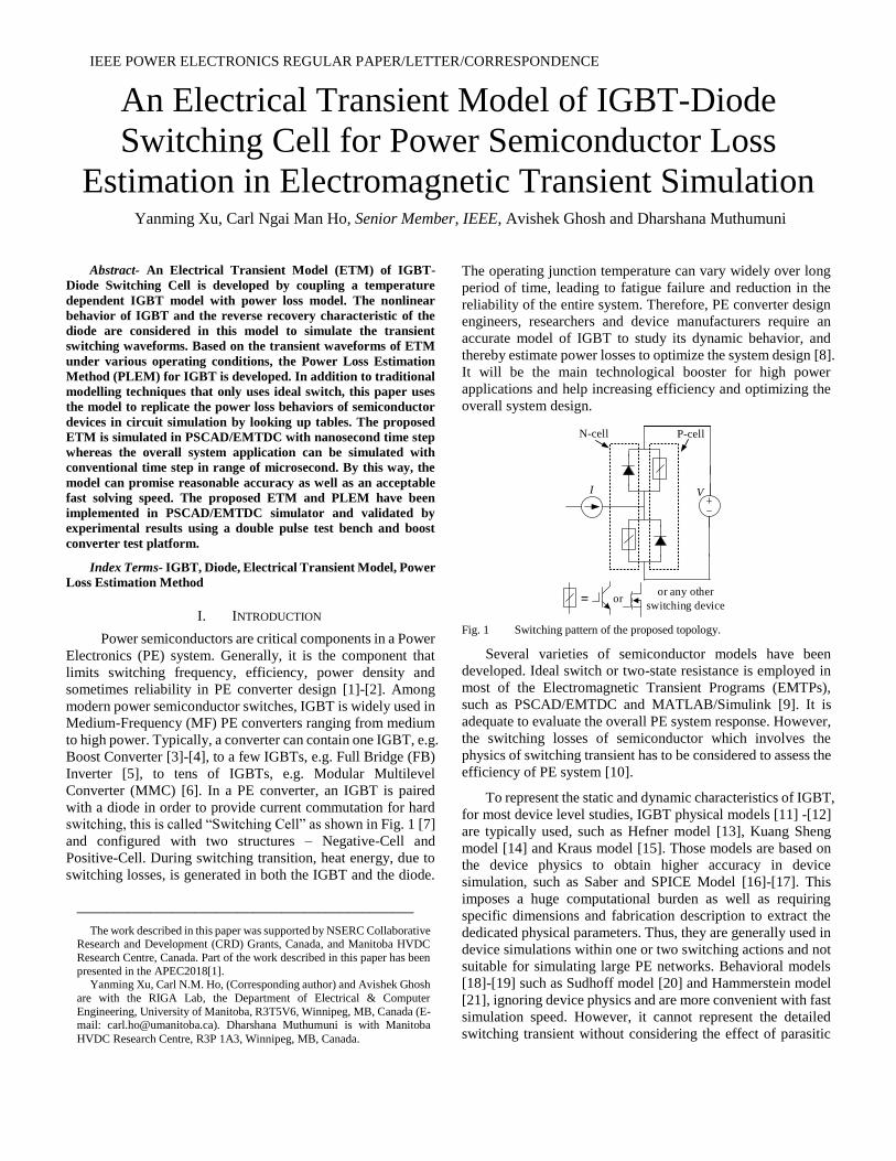
switching, this is called “Switching Cell” as shown in Fig. 1 [7]
and configured with two structures – Negative-Cell and
Positive-Cell. During switching transition, heat energy, due to
switching losses, is generated in both the IGBT and the diode.
The operating junction temperature can vary widely over long
period of time, leading to fatigue failure and reduction in the
reliability of the entire system. Therefore, PE converter design
engineers, researchers and device manufacturers require an
accurate model of IGBT to study its dynamic behavior, and
thereby estimate power losses to optimize the system design [8].
It will be the main technological booster for high power
applications and help increasing efficiency and optimizing the
overall system design.
Fig. 1 Switching pattern of the proposed topology.
Several varieties of semiconductor models have been
developed. Ideal switch or two-state resistance is employed in
most of the Electromagnetic Transient Programs (EMTPs),
such as PSCAD/EMTDC and MATLAB/Simulink [9]. It is
adequate to evaluate the overall PE system response. However,
the switching losses of semiconductor which involves the
physics of switching transient has to be considered to assess the
efficiency of PE system [10].
To represent the static and dynamic characteristics of IGBT,
for most device level studies, IGBT physical models [11] -[12]
are typically used, such as Hefner model [13], Kuang Sheng
model [14] and Kraus model [15]. Those models are based on
the device physics to obtain higher accuracy in device
simulation, such as Saber and SPICE Model [16]-[17]. This
imposes a huge computational burden as well as requiring
specific dimensions and fabrication description to extract the
dedicated physical parameters. Thus, they are generally used in
device simulations within one or two switching actions and not
suitable for simulating large PE networks. Behavioral models
[18]-[19] such as Sudhoff model [20] and Hammerstein model
[21], ignoring device physics and are more convenient with fast
simulation speed. However, it cannot represent the detailed
switching transient without considering the effect of parasitic
V
P-cell
I
N-cell
= oror any other
switching device
______________________________________________
The work described in this paper was supported by NSERC Collaborative Research and Development (CRD) Grants, Canada, and Manitoba HVDC
Research Centre, Canada. Part of the work described in this paper has been
presented in the APEC2018[1]. Yanming Xu, Carl N.M. Ho, (Corresponding author) and Avishek Ghosh
are with the RIGA Lab, the Department of Electrical & Computer
Engineering, University of Manitoba, R3T5V6, Winnipeg, MB, Canada (E-mail: [email protected]). Dharshana Muthumuni is with Manitoba
HVDC Research Centre, R3P 1A3, Winnipeg, MB, Canada.

IEEE POWER ELECTRONICS REGULAR PAPER/LETTER/CORRESPONDENCE
parameters and reverse recovery of diode which is significant
for estimating switching losses in various operating conditions.
Electrothermal models [22]-[24] considering electrical and
thermal couplings involved in the system are able to help
solving heat-flow problem and taking temperature effect into
account. However, multi-dimensional thermal model and
package properties consideration will increase the complexity
of the model which is difficult to implement in simulator. The
choice of IGBT model depends on the required accuracy,
complexity, convergence properties and simulation time.
For accurate estimation of power loss, one approach is
curving fitting the loss curve directly or deriving specially
defined analytical loss equations based on the switching
transient waveforms from measurement, datasheet or device
simulation [25]-[28]. In this way, the accuracy is limited by the
specific operating conditions and a mass of device test may be
involved. EMT simulation-based loss calculation methods [29]-
[30] use specially developed algebraic equations to piecewise
linearize the switching waveforms and externally estimate the
device losses with simple switches in system simulation.
However, it involves complicated mathematical formulae and
parameter extractions without enough temperature
consideration. Besides, IGBT Thermo-Sensitive Electrical
Parameters (TSEPs), such as on-state voltage ( 𝑣𝑐𝑒𝑠𝑎𝑡 ),
threshold voltage (𝑉𝑡 ), trans-conductance (𝐾𝑝 ) will change
depending on the operating temperature, which also should be
considered [31]-[32].
This paper proposes a comprehensive PE system simulation
method, which uses temperature-dependent ETM to simulate
static and dynamic behaviors of IGBT-Diode Switching Cell in
order to determine semiconductor losses during the PE system
simulation. There are two technical contributions in this paper.
1) An IGBT-Diode switching cell behavioral model is
proposed. Various parameters including tail current, miller
plateau voltage, nonlinear parasitic elements of IGBT and
reverse recovery current of diode have been taken into account.
All the parameters of the model are extracted from device
datasheet considering the temperature sensitivity.
2) A Power Loss Estimation Method (PLEM) is
developed based on the transient simulation waveforms to
calculate the power dissipation of IGBT and Diode. And the
loss information is connected to the EMTPs circuit simulator,
e.g. PSCAD with simple switch model through look up table in
PE system simulation. In other words, the switching loss
models are integrated into the software (PSCAD) and the
system simulation process.
With this approach, the speed of PE simulation can be
maintained and acceptable accuracy of power loss estimation
can be achieved. The model parameter extraction sequence has
also been developed to characterize various IGBTs based on the
device datasheet. The completed model and method were
implemented in PSCAD/EMTDC and verified by experimental
results using a double pulse test bench as well as a boost
converter test bed.
Fig. 2 Block diagram of power loss estimation in a circuit simulation.
II. SIMULATION STRATEGY OF POWER SEMICONDUCTOR
LOSSES
In order to provide fast and accurate semiconductor loss
estimation in a PE circuit simulation in an EMTP simulator e.g.
PSCAD, a simulation strategy is proposed. A simplified block
diagram of the proposed simulating process including two
stages in the simulating platform is shown in Fig. 2.
A. Device Level Simulation
Before simulating an overall PE system, a device level
simulation will be done to create 4-Dimensional (4D) Look-Up-
Tables (LUT) representing transient losses. It generates the loss
tables including turn-on, turn-off, reverse recovery and
conduction losses based on the simulation conditions (e.g.
Junction Temperature (𝑇𝑗), Voltage (𝑉𝑑𝑑) and Current (𝐼𝐿) and
power device parameters (e.g. Input capacitance (𝐶𝑖𝑠𝑠), Reverse
recovery peak current ( 𝐼𝑟𝑚 ). The semiconductor parameters
which are extracted from datasheet by curve fitting or empirical
formulas and the simulation conditions are the inputs to the
proposed IGBT-Diode Switching Cell ETM for simulating the
detailed switching waveforms. Based on the waveforms, the
power losses under various operating conditions which export
as a power loss table can be computed by the PLEM. The ETM
and the PLEM are applied in the device simulation with
nanosecond (ns) time step for the reason of high accuracy. Since
only several tens of points will be simulated, it will require only
a short computational time.
B. Circuit Level Simulation
The obtained LUT in device level simulation works as an
interface between the simulations of device and circuit levels.
PSCAD simulates the system using an ideal switch model in
microsecond (µs) time-step. It inputs instantaneous 𝑇𝑗, 𝑉𝑑𝑑, and
𝐼𝐿 values to the LUT during each switching action, and
computes switching loss and conduction power by interpolation.
Furthermore, time varying instantaneous power loss waveforms
can be obtained by taking the integral of the energy loss
information, which will provide both static and dynamic system
loss information to users. This is a simple search method and
mathematics, and will not significantly increase the
computational time when comparing to the current PSCAD
simulator that uses an ideal model or involving device
simulation in circuit simulations.
Power Loss
Estimation
Device-Level
Simulation(ns)
Power
Electrical
Network
...
Circuit-Level
Simulation(µs)
Loss Table
Electrical
Transient
Model
(ETM)0 t0 t1 t2 t3 t4 t5 t6 t7 t8
Vce
Ic
Vsat
ic(t)vce(t)
vge(t)
Vt
Vplateau
Vdd
IL
Irm+IL
t9
Power Loss
Model
Tj
Pt
Vdd
IL
Switching Cell
Pon (Vdd, IL, Tj)
Poff (Vdd, IL, Tj)
Pcon(Vdd, IL, Tj)
Pt (Vdd, IL, Tj)
Vdd
IL
P Loss
Tj = 25
Tj = 50
Tj =150
IEEE POWER ELECTRONICS REGULAR PAPER/LETTER/CORRESPONDENCE
(a)
(b)
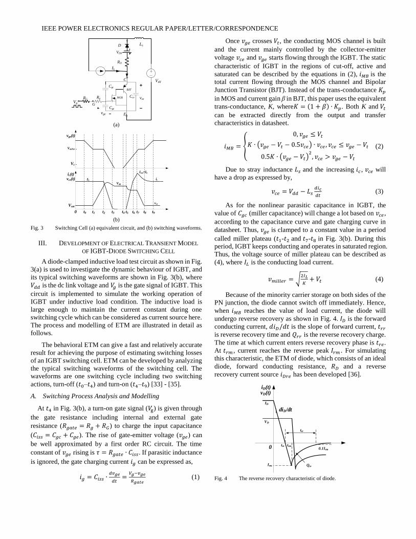
Fig. 3 Switching Cell (a) equivalent circuit, and (b) switching waveforms.
III. DEVELOPMENT OF ELECTRICAL TRANSIENT MODEL
OF IGBT-DIODE SWITCHING CELL
A diode-clamped inductive load test circuit as shown in Fig.
3(a) is used to investigate the dynamic behaviour of IGBT, and
its typical switching waveforms are shown in Fig. 3(b), where
𝑉𝑑𝑑 is the dc link voltage and 𝑉𝑔 is the gate signal of IGBT. This
circuit is implemented to simulate the working operation of
IGBT under inductive load condition. The inductive load is
large enough to maintain the current constant during one
switching cycle which can be considered as current source here.
The process and modelling of ETM are illustrated in detail as
follows.
The behavioral ETM can give a fast and relatively accurate
result for achieving the purpose of estimating switching losses
of an IGBT switching cell. ETM can be developed by analyzing
the typical switching waveforms of the switching cell. The
waveforms are one switching cycle including two switching
actions, turn-off (𝑡0–𝑡4) and turn-on (𝑡4–𝑡9) [33] - [35].
A. Switching Process Analysis and Modelling
At 𝑡4 in Fig. 3(b), a turn-on gate signal (𝑉g) is given through
the gate resistance including internal and external gate
resistance (𝑅𝑔𝑎𝑡𝑒 = 𝑅𝑔 + 𝑅𝐺) to charge the input capacitance
(𝐶𝑖𝑠𝑠 = 𝐶𝑔𝑐 + 𝐶𝑔𝑒). The rise of gate-emitter voltage (𝑣𝑔𝑒) can
be well approximated by a first order RC circuit. The time
constant of 𝑣𝑔𝑒 rising is 𝜏 = 𝑅𝑔𝑎𝑡𝑒 ∙ 𝐶𝑖𝑠𝑠. If parasitic inductance
is ignored, the gate charging current 𝑖𝑔 can be expressed as,
𝑖𝑔 = 𝐶𝑖𝑠𝑠 ∙𝑑𝑣𝑔𝑒
𝑑𝑡=
𝑉𝑔−𝑣𝑔𝑒
𝑅𝑔𝑎𝑡𝑒 (1)
Once 𝑣𝑔𝑒 crosses 𝑉𝑡, the conducting MOS channel is built
and the current mainly controlled by the collector-emitter
voltage 𝑣𝑐𝑒 and 𝑣𝑔𝑒 starts flowing through the IGBT. The static
characteristic of IGBT in the regions of cut-off, active and
saturated can be described by the equations in (2), 𝑖𝑀𝐵 is the
total current flowing through the MOS channel and Bipolar
Junction Transistor (BJT). Instead of the trans-conductance 𝐾𝑝
in MOS and current gain β in BJT, this paper uses the equivalent
trans-conductance, K, where𝐾 = (1 + 𝛽) ∙ 𝐾𝑝. Both K and 𝑉𝑡
can be extracted directly from the output and transfer
characteristics in datasheet.
𝑖𝑀𝐵 =
0, 𝑣𝑔𝑒 ≤ 𝑉𝑡
𝐾 ∙ (𝑣𝑔𝑒 − 𝑉𝑡 − 0.5𝑣𝑐𝑒) ∙ 𝑣𝑐𝑒 , 𝑣𝑐𝑒 ≤ 𝑣𝑔𝑒 − 𝑉𝑡
0.5𝐾 ∙ (𝑣𝑔𝑒 − 𝑉𝑡)2, 𝑣𝑐𝑒 > 𝑣𝑔𝑒 − 𝑉𝑡
(2)
Due to stray inductance 𝐿𝑠 and the increasing 𝑖𝑐 , 𝑣𝑐𝑒 will
have a drop as expressed by,
𝑣𝑐𝑒 = 𝑉𝑑𝑑 − 𝐿𝑠𝑑𝑖𝑐
𝑑𝑡 (3)
As for the nonlinear parasitic capacitance in IGBT, the
value of 𝐶𝑔𝑐 (miller capacitance) will change a lot based on 𝑣𝑐𝑒 ,
according to the capacitance curve and gate charging curve in
datasheet. Thus, 𝑣𝑔𝑒 is clamped to a constant value in a period
called miller plateau (𝑡1-𝑡2 and 𝑡7-𝑡8 in Fig. 3(b). During this
period, IGBT keeps conducting and operates in saturated region.
Thus, the voltage source of miller plateau can be described as
(4), where 𝐼𝐿 is the conducting load current.
𝑣𝑚𝑖𝑙𝑙𝑒𝑟 = √2𝐼𝐿
𝐾+ 𝑉𝑡 (4)
Because of the minority carrier storage on both sides of the
PN junction, the diode cannot switch off immediately. Hence,
when 𝑖𝑀𝐵 reaches the value of load current, the diode will
undergo reverse recovery as shown in Fig. 4. 𝐼𝐷 is the forward
conducting current, 𝑑𝑖𝐷/𝑑𝑡 is the slope of forward current, 𝑡𝑟𝑟
is reverse recovery time and 𝑄𝑟𝑟 is the reverse recovery charge.
The time at which current enters reverse recovery phase is 𝑡𝑟𝑒.
At 𝑡𝑟𝑚 , current reaches the reverse peak 𝐼𝑟𝑚 . For simulating
this characteristic, the ETM of diode, which consists of an ideal
diode, forward conducting resistance, 𝑅𝐷 and a reverse
recovery current source 𝑖𝐷𝑟𝑒 has been developed [36].
Fig. 4 The reverse recovery characteristic of diode.
Vdd
G
E
Cce
Cgc
Cge
Rg MOS
BJT
Vg
RG
vge
vce
C
RD
VD0
D
IL
Ls
0 t0 t1 t2 t3 t4 t5 t6 t7 t8
vce
ic
Vsat
ic(t)vce(t)
vge(t)
Vt
Vmiller
Vdd
IL
Irm+IL
t9
0tre trm
0.1Irm
VD
iD(t)vD(t)
trr
Irm
ID
diD/dt
Qrr
IEEE POWER ELECTRONICS REGULAR PAPER/LETTER/CORRESPONDENCE
In a switching cell, current will go through IGBT and diode
alternatively. Hence, every time the diode turns off and starts
reverse recovery, an additional over current will add to the
paired IGBT. This interaction is expressed in (5) and the
parameters are calculated by (6) according to the datasheet. 𝑖𝐷𝑟𝑒
is the reverse recovery current of the Free-Wheeling Diode
(FWD). The decay time constant of the reverse recovery 𝜏𝑟𝑒
and 𝑅𝐷 can be extracted from diode curve using curve fitting.
𝑖𝐷𝑟𝑒 =
𝑑𝑖𝐷
𝑑𝑡(𝑡 − 𝑡𝑟𝑒), 𝑡𝑟𝑒 < 𝑡 < 𝑡𝑟𝑚
𝐼𝑟𝑚𝑒−𝑡−𝑡𝑟𝑚𝜏𝑟𝑒 , 𝑡 > 𝑡𝑟𝑚
(5)
𝜏𝑟𝑒 =
1
𝑙𝑛10(𝑡𝑟𝑟 −
𝐼𝑟𝑚𝑑𝑖𝐷𝑑𝑡
)
𝐼𝑟𝑚 = √𝑄𝑟𝑟 ∙ 𝑑𝑖𝐷/𝑑𝑡
𝑡𝑟𝑟 = 2√𝑄𝑟𝑟/𝑑𝑖𝐷/𝑑𝑡
(6)
As soon as the reverse recovery current of diode reaches
peak value, 𝑣𝑐𝑒 drops to the forward conducting voltage 𝑣𝑐𝑒𝑠𝑎𝑡 . Meanwhile, 𝑣𝑔𝑒 increase slowly until it climbs to𝑉𝑔.
The turn-off process is almost the inverse sequence of the
turn on process, except the tail current period. During the IGBT
turn-off transient, the excess base carrier recombination makes
the shutdown current tailing time longer. Besides the
conventional equations, an additional equation has been derived
to completely represent this nonlinear characteristics in ETM.
In the calculation, the tail current can be described by the
exponential function (7). 𝜏 is the carrier transit time. t is the
simulation time and 𝑡0 is the initial time of the tail current. 𝐼𝑡𝑎𝑖𝑙0
is the collector current at the start of the tailed stage.
𝑖𝑀𝐵 = 𝐼𝑡𝑎𝑖𝑙0 ∙ 𝑒−𝑡−𝑡0𝜏 , (𝑣𝑔𝑒 < 𝑉𝑡 , Turn off) (7)
B. Temperature Sensitive Parameters Consideration
Temperature Sensitive Electrical Parameters (TSEPs) are
today widely used for temperature measurement. With various
temperature, electrical parameters of IGBT such as 𝑣𝑐𝑒𝑠𝑎𝑡, 𝑉𝑡, K, and carrier lifetime (τ), will change and affect the dynamic
behaviour. Thus it also should be under consideration for high
accuracy simulation. Therefore, this paper use a series of
following equations to describe the TSEPs in IGBT and diode.
It should be noted that all the equations are based on the
experimental measurement and curve fitting as a function of
temperature and various parameters [31].
𝑉𝑡 = 𝑉𝑡0 − 𝐾𝑡 ∙ (𝑇𝑗 − 𝑇𝑎)
𝐾 = 𝐾0 ∙ (𝑇𝑎
𝑇𝑗)0.8
𝜏 = 5 × 10⁻⁷ ∙ (𝑇𝑎
𝑇𝑗)1.5
(8)
𝑉𝑐𝑒𝑠𝑎𝑡 = (𝑉𝑐𝑒𝑠𝑎𝑡0 + 𝑟0𝑖𝑐) + (∆𝑉𝑐𝑒𝑠𝑎𝑡 + ∆𝑟0𝑖𝑐)(𝑇𝑗 − 𝑇𝑎)
𝐼𝑟𝑚 = 𝐼𝑟𝑚0 + 𝑡𝑟𝑚𝑑𝑖𝐷
𝑑𝑡+ (𝐾𝑟𝑚 + 𝐾𝑡𝑟𝑚
𝑑𝑖𝐷
𝑑𝑡) (𝑇𝑗 − 𝑇𝑎)
𝑄𝑟𝑟 = 𝑄𝑟𝑟0 + 𝑡𝑄𝑟𝑟𝑑𝑖𝐷
𝑑𝑡+ (𝐾𝑟𝑟 + 𝐾𝑄𝑟𝑟
𝑑𝑖𝐷
𝑑𝑡) (𝑇𝑗 − 𝑇𝑎)
(9)
TABLE I TSEPS OF IGBT AND DIODE
Parameter Value Parameter Value
𝑉𝑡0 5.812 𝐼𝑟𝑚0 17.77
𝐾𝑡 0.009988 𝑡𝑟𝑚 0.01234
𝐾0 2.834 𝐾𝑟𝑚 0.04136
𝑉𝑐𝑒𝑠𝑎𝑡0 0.9715 𝐾𝑡𝑟𝑚 0.000035
𝑟0 0.02153 𝑄𝑟𝑟0 3.602
∆𝑉𝑐𝑒𝑠𝑎𝑡 -0.001 𝑡𝑄𝑟𝑟 0.0003
∆𝑟0 0.0001059 𝐾𝑟𝑟 0.03
𝑇𝑎 25 ºC 𝐾𝑄𝑟𝑟 0.00000722
𝑇𝑎 is the initial ambient temperature. 𝑇𝑗 is the operating
junction temperature. All the curve fitting parameters can be
obtained from datasheet. According to equation (8) and (9),
TSEPs can be calculated under various junction temperature
and operating conditions and input to switching transient
simulation in PSCAD/EMTDC. The TSEPs of the model are
extracted from the junction temperature related curves in
datasheet of Infineon IKW40T120 IGBT using MATLAB for
curve fitting as shown in Table I.
C. Proposed Model Circuit of IGBT and Diode
IGBT is pseudo Darlington structure, which consists of an
N-channel MOSFET and a PNP BJT whose base current is
controlled by the MOSFET gate voltage. Based on that, the
corresponding schematic of the proposed ETM of an IGBT and
a diode are shown in Fig. 5. 𝐿𝑠 is the circuit parasitic inductance.
The equivalent miller-plateau voltage source 𝑣𝑚𝑖𝑙𝑙𝑒𝑟 works
during miller plateau time mentioned above. Also the
conducting voltage source 𝑣𝑐𝑒𝑠𝑎𝑡 operates during IGBT
conducting period. The ETM is formulated in PSCAD/EMTDC
including main circuit, custom programed models and other
signal control components. The main circuit is implemented by
basic electronic components with controlled voltage and current
source. The value of TSEPs are updated and calculated by the
custom programed model based the temperature feature and the
input operating conditions. Furthermore, the nonlinear features
of IGBT and reverse recovery characteristic of body diode are
also programed using FORTRAN to control the voltage and
current source respectively. Thus, the transient waveforms of
switching cell can be simulated and the switching time as well
as other transient parameters can be further extended to power
loss calculation model.
Fig. 5 The proposed transient model circuit of IGBT-Diode switching cell.
Vdd
G
E
Rg
vg
RG
C
RD
D
IL
Ll
Ls
iDre
vcesatiMB
Ciss
vmiller
ic

IEEE POWER ELECTRONICS REGULAR PAPER/LETTER/CORRESPONDENCE
IV. POWER LOSS ESTIMATION METHOD OF IGBT-DIODE
SWITCHING CELL
Once the switching transient waveforms are obtained by the
ETM mentioned in the previous section, the PLEM is
developed to analyse and calculate the power loss of IGBT. For
simplicity, in Fig. 3 (b) the voltage and current are assumed
piecewise linear changing except in region 𝑡3 to 𝑡4 and 𝑡7 to 𝑡9. The tailing time, 𝑡𝑡𝑎𝑖𝑙 , is defined as the time period when 𝑖𝑐 decreases from 10% 𝐼𝐿 to 1% 𝐼𝐿 . In addition, the diode reverse
recovery is very short after 𝑡7 and the loss is neglected. All the
following switching period in the expressions can be obtained
in the ETM simulation [37].
The main part of the power loss during turn-off period
occurs from t1 to t3 and the tailing current period in Fig. 3(b).
The total turn-off loss includes the voltage slope loss 𝐸𝑜𝑓𝑓𝑉 , the
current slope loss 𝐸𝑜𝑓𝑓𝐼 and the tail current loss, 𝐸𝑜𝑓𝑓𝑇 .
In the interval [𝑡1, 𝑡2], the current 𝑖𝑐 has the same value as
𝐼𝐿 and the voltage 𝑣𝑐𝑒 increases from 0 to 𝑉𝑑𝑑. Therefore, the
power loss during this period 𝑡𝑜𝑓𝑓𝑉 is given by
𝐸𝑜𝑓𝑓𝑉 = 0.5𝐼𝐿𝑉𝑑𝑑𝑡𝑜𝑓𝑓𝑉 (10)
If 𝑣𝑐𝑒 is assumed constant during the interval [𝑡2, 𝑡3], the
resulting power loss is,
𝐸𝑜𝑓𝑓𝐼 =𝐼𝐿𝑉𝑑𝑑
2∙ 𝑡𝑜𝑓𝑓𝐼 + 0.5𝐿𝑠𝐼𝐿
2 (11)
Assuming the current starts tailing when 10% of 𝐼𝐿 and the
time constant τ equals to 𝑡𝑡𝑎𝑖𝑙/𝑙𝑛10, the power loss caused by
the tail current during the period 𝑡𝑡𝑎𝑖𝑙 can be estimated as
𝐸𝑜𝑓𝑓𝑇 = 𝑉𝑑𝑑 ∫ 𝑒−𝑡
𝜏𝑑𝑡𝑡𝑡𝑎𝑖𝑙0
=0.456𝐼𝐿𝑉𝑑𝑑
𝑡𝑡𝑎𝑖𝑙 (12)
A similar analysis is carried out to calculate the turn-on
power loss from t5 to t8. The total turn-on power loss includes
the current slope, 𝐸𝑜𝑛𝐼 , the voltage slope, 𝐸𝑜𝑛𝑉 and the reverse
recovery loss 𝐸𝑜𝑛𝑖𝑟𝑟 .
The power loss for the interval [𝑡5 , 𝑡6] characterized by
increasing 𝑖𝑐 can be expressed as
𝐸𝑜𝑛𝐼 = 0.5𝐼𝐿𝑉𝑑𝑑𝑡𝑜𝑛𝐼 − 0.5𝐿𝑠𝐼𝐿2 (13)
Assuming that the current 𝑖𝑐 = 𝐼𝐿 during the voltage slope
interval [𝑡7, 𝑡8], the power loss becomes
𝐸𝑜𝑛𝑉 = 0.5𝐼𝐿𝑉𝑑𝑑𝑡𝑜𝑛𝑉 (14)
As for the diode reverse recovery power loss during the
period 𝑡𝑟𝑟, we assume it is very short with respect to the voltage
slope interval. Under this assumption, the power loss caused by
the reverse recovery charge 𝑄𝑟𝑟 is given by
𝐸𝑜𝑛𝑖𝑟𝑟 = (𝑉𝑑𝑑 −𝐿𝑠𝐼𝐿
𝑡𝑜𝑛𝐼)(𝐼𝐿 ∙ (𝑡𝑟𝑚 − 𝑡𝑟𝑒) + 𝑄𝑟𝑟) (15)
From the output characteristics of IGBT and diode in
datasheet, the on-state voltage can be represented in terms of
on-state zero current collector-emitter voltage 𝑉𝑐𝑒0 and
resistance 𝑟𝑐 .
𝑣𝑐𝑒𝑠𝑎𝑡 = 𝑉𝑐𝑒0 + 𝑟𝑐𝑖𝑐 (16)
If the average current is 𝐼𝑐𝑎𝑣 and the rms value is 𝐼𝑐𝑟𝑚𝑠, then
the average conduction loss of IGBT is as following, where 𝑓𝑠𝑤
is the switching frequency of IGBT.
𝑃𝑐𝐼𝐺𝐵𝑇 = 𝑓𝑠𝑤 ∫ 𝑣𝑐𝑒𝑖𝑐𝑑𝑡1/𝑓𝑠𝑤0
= 𝑉𝑐𝑒0𝐼𝑐𝑎𝑣 + 𝑟𝑐𝐼𝑐𝑟𝑚𝑠2 (17)
The total switching power loss 𝐸𝑡𝑠 can be estimated as the
sum of the loss equations above, and the total IGBT loss power
is expressed in (18).
𝐸𝑡𝑠 = 𝐸𝑜𝑓𝑓𝑉 + 𝐸𝑜𝑓𝑓𝐼 + 𝐸𝑜𝑓𝑓𝑇 + 𝐸𝑜𝑛𝐼 + 𝐸𝑜𝑛𝑉 + 𝐸𝑖𝑟𝑟 (18)
From the observation of the set of equations above, 𝑉𝑑𝑑 and
𝐼𝐿 are the key parameters affecting the power loss. In addition,
the effects of diode reverse recovery current, parasitic stray
inductance and tail current must also be considered at high
switching frequency.
V. IMPLEMENTATION IN SIMULATOR AND EXPERIMENT
VERIFICATIONS
The ETM and PLEM have been proposed in this paper. The
key objective of the model and the method is to estimate the
power dissipation of semiconductors in a PE system simulation
based on the ETM waveforms. The model and the method are
implemented in PSCAD/EMTDC and validated by comparing
with the experimental results of double pulse tester and a boost
converter. Generally, to use the proposed model, the parameters
of the selected Si IGBT device need to be extracted from its
datasheet by curve fitting or mathematic methods. Then the
device simulation can be multiple run with nano-second (ns)
time step according to the setting range of the operating
conditions. The power loss data based on the simulated
waveforms can be further exported and reformatted as look up
table for power loss prediction in system simulation.
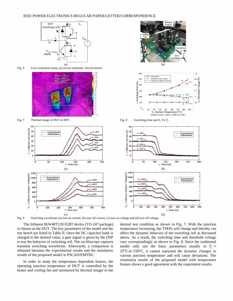
A. Device Level Model Validation
Based on the circuit in Fig. 6(a), a Double Pulse Test (DPT)
bench is designed and implemented for characterization of the
IGBT and the diode. The test setup consists of power supply,
Digital Signal Processing (DSP) control system, thermal
control system, cooling fan and the Device Under Test (DUT)
as shown in Fig. 6(b). A thermocouple is placed between
heatsink and the IGBT device to measure the case temperature.
Through the thermocouple amplifier AD595, the value of
temperature is further read by the analog pin of DSP. The
temperature in DPT is controlled to the test condition by the
heater attached to the heatsink and cooling fan as well as the
DSP controller. And the thermal imager Tis40 is used in DPT
for monitoring the junction temperature of the device.
TABLE II PARAMETERS OF DEVICE AND TEST BED
Parameter Value Parameter Value
𝑅𝑔 6Ω 𝐶𝑖𝑠𝑠 2500pF
𝑉𝑡 5.8V 𝐶𝑟𝑠𝑠 110pF
𝐾 2.834 A/V2 𝑅𝐺 15Ω
𝑉𝑑𝑑 0-1kV 𝐿𝑙 5mH
𝐼𝐿 0-80A 𝐿𝑠 180nH
IEEE POWER ELECTRONICS REGULAR PAPER/LETTER/CORRESPONDENCE
(a) (b)
Fig. 6 Loss evaluation setup, (a) circuit schematic, (b) test bench.
Fig. 7 Thermal image of DUT in DPT.
Fig. 8 Switching time and 𝑉𝑡 Vs 𝑇𝑗.
(a) (b)
(c) (d)
Fig. 9 Switching waveforms (a) turn on current, (b) turn off current, (c) turn on voltage and (d) turn off voltage.
The Infineon IKW40T120 IGBT device (TO-247 package)
is chosen as the DUT. The key parameters of the model and the
test bench are listed in Table II. Once the DC capacitor bank is
charged to the desired value, a gate signal is given by the DSP
to test the behavior of switching cell. The oscilloscope captures
transient switching waveforms. Afterwards, a comparison is
obtained between the experimental results and the simulation
results of the proposed model in PSCAD/EMTDC.
In order to study the temperature dependent feature, the
operating junction temperature of DUT is controlled by the
heater and cooling fan and monitored by thermal imager to the
desired test condition as shown in Fig. 7. With the junction
temperature increasing, the TSEPs will change and thereby can
affect the dynamic behavior of the switching cell as discussed
above. As a result, the switching time and threshold voltage
vary correspondingly as shown in Fig. 8. Since the traditional
model only use the basic parameters usually in 𝑇𝑗 =
25 or 150 , it cannot represent the dynamic changes in
various junction temperature and will cause deviations. The
simulation results of the proposed model with temperature
feature shows a good agreement with the experiment results.
Vdd
vg
vge
vce
ic
iL
iD
Ll
LsDUT
Switching Cell
DUT
Switching Cell
Gate driver
Thermal
Control
Cooling
Fan
0 20 40 60 80 100 120 140 1600
50
100
150
200
250
300
Tj, Junction Temperature [°C]
t, S
wit
ch
ing T
ime
[ns]
Vt, T
hresh
old
Volt
age [
V]
2.5
5
7.5
10
12.5
15
tf
tr
Vt
Experiment
Simulation with Tj feature
Simulation without Tj feature 11.3%
23.95%
1.93%
(Inductive load, IL=40A,Vdd=600V, Rg=15 )
0 50 100 150 200 250
30
40
50
60
10
20
0
ExperimentSimulation
IL=40A
IL=20A
IL=10A
i c ,
Coll
ecto
r cu
rren
t [A
]
t , Time [ns]
IL=30A
0 50 100 150 200 250 300
0
60
ExperimentSimulation
i c ,
Co
llec
tor
curr
ent
[A]
t , Time [ns]
50
40
20
30
10
IL=40A
IL=30A
IL=20A
IL=10A
0 100 200 300 400 500 600
0
200
400
600
800
1000
1200
ExperimentSimulation Vdd=800V
Vdd=600V
Vdd=400V
Vdd=200V
t , Time [ns]
Vce
, C
oll
ecto
r-E
mit
ter V
olt
ag
e[V
]
0 100 200 300 400 500 600 700 800 900
0
1000
1200
800
600
400
200
ExperimentSimulation
t , Time [ns]
Vce
, C
oll
ecto
r-E
mit
ter V
olt
age[V
]
Vdd=800V
Vdd=600V
Vdd=400V
Vdd=200V

IEEE POWER ELECTRONICS REGULAR PAPER/LETTER/CORRESPONDENCE
(a) (b) (c)
Fig. 10 Switching loss (a) vs 𝑖𝑐, (b) vs 𝑣𝑐𝑒 , (c) vs 𝑇𝑗 .
Fig. 11 3D plot of switching loss (𝑇𝑗=150).
(a)
(b)
Fig. 12 Boost converter setup, (a) block diagram, and (b) testbed.
Fig. 9 shows the turn-on and turn-off of IGBT collector
current and collector-emitter voltage transient waveforms under
the test condition (𝑇𝑗 = 150). The switching details such as
current and voltage spikes, tail current, interaction of diode
reverse recovery and the effect of parasitic inductance and
capacitance are clearly seen from the transient waveforms.
Because of the parasitic parameters of the test bench, there are
small oscillations of current after IGBT completely turning on
which is not considered in the model. The PSCAD simulation
results show good agreement with the experimental results.
The computed power losses in simulation by PLEM are also
compared with the measured results which are obtained by
integrating the product of measured voltage and current during
switching process in Fig. 10. A series of load voltage and
current can be set to obtain the power loss table by the multiply-
run function in PSCAD. As can be seen in Fig. 10, the switching
loss changes with the voltage, current and temperature
increasing as well as the proportion of turn-on and -off losses.
The simulation results have reasonable accuracy with variation
of voltage and current especially in rated operating condition.
Fig. 11 shows an example of a 3D plot of losses. Although only
one layer is graphically demonstrated in Fig. 11, multiple layers
with various temperatures are resulted in the simulator. A 4-D
table is stored in the simulator and ready for circuit simulations.
B. System Level Model Validation
The proposed model can be applied to various PE
applications such as buck or boost converter for semiconductor
loss estimation. In order to evaluate the switching cell model
and switching losses of a converter simulating in PSCAD, a
boost converter, shown in Fig. 12(a), is implemented in PSCAD
using the proposed model and methods. The corresponding
boost converter test bed with cooling system shown in Fig. 12(b)
has been designed and implemented for validation of the
simulations. The main parameters of the test bed are listed in
Table III. The designed boost converter setup includes the main
circuit board, DC power supply, oscilloscope, resistive load and
other measure equipment. The same semiconductor, Infineon
IKW40T120 IGBT, is used for testing. Wakefield-Vette 394-
2AB heat sink is chosen as the cooling system.
TABLE III PARAMETERS OF BOOST CONVERTER
Parameter Value Parameter Value
𝑣𝑠 150V 𝑣𝑜 300V
L 7.17mH 𝐶𝑜 940µF
𝑅 77Ω 𝑓𝑠𝑤 10kHz
Duty cycle 0.5 𝑅𝐺 15Ω
0 10 20 30 40 50 60 70 800
5
10
15
20
25
30
E,
Sw
itch
ing
En
erg
y L
oss
[m
J]
ic, Collector Current [A]
Ets
Eon
Eoff
ExperimentSimulation
400 500 600 700 800 9000
5
10
15
20
Ets
Eon
Eoff
E,
Sw
itch
ing
En
erg
y L
oss
[m
J] Experiment
Simulation
vce, Collector-Emitter Voltage [V]
0 0 20 40 60 80 100 120 140 1600
5
10
15
Tj, Junction Temperature [°C]
E, S
wit
ch
ing
En
erg
y L
oss
[m
J]
ExperimentSimulation
Ets
Eon
Eoff
060
10
100040
20
800600
30
20 400200
0 0
vce [V]ic [A]
Ets, S
wit
ch
ing
En
erg
y L
oss
[mJ]
vs
D.U.T
(Switch Cell)io
vo
RCo
G
iL 0PWM
Heatsink
vs
ic
iL
io
L
Cin
vcevoDSP Controller
Boost
Converter
D.U.T
Switch Cell
DC
Power Supply
Oscilloscope
Power Supply
Computer
Monitor
DSP
Controller
D.U.T
Switch Cell
Heatsink
Inductor
DSP
Controller
Gate Driver Capacitors
Resistive
Load
IEEE POWER ELECTRONICS REGULAR PAPER/LETTER/CORRESPONDENCE
(a) (b)
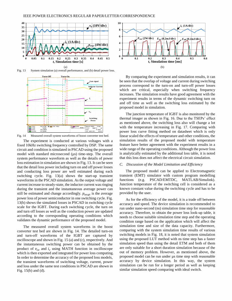
Fig. 13 System simulation (a) overall performance, and (b) detail power loss.
Fig. 14 Measured overall system waveforms of boost converter test bed.
The experiment is conducted at various voltages with a
fixed 10kHz switching frequency controlled by DSP. The same
circuit and condition is simulated in PSCAD using the proposed
model with standard microsecond (µs) time-step. The overall
system performance waveform as well as the details of power
loss estimation in simulation are shown in Fig. 13. It can be seen
that the detail loss power including turn on and off power losses
and conducting loss power are well estimated during each
switching cycle. Fig. 13(a) shows the start-up transient
waveforms in the PSCAD simulation. As the output voltage and
current increase to steady-state, the inductor current was ringing
during the transient and the instantaneous average power can
still be estimated and change accordingly. 𝑝𝑎𝑣𝑔𝑡 is the average
power loss of power semiconductor in one switching cycle. Fig.
13(b) shows the simulated losses in PSCAD in switching cycle
scale for the IGBT. During each switching cycle, the turn on
and turn off losses as well as the conduction power are updated
according to the corresponding operating conditions which
validates the dynamic performance of the proposed model.
The measured overall system waveforms in the boost
converter test bed are shown in Fig. 14. The detailed turn-on
and turn-off waveforms of the IGBT are captured by
oscilloscope and shown in Fig. 15 (a) and (c), respectively. And
the instantaneous switching power can be obtained by the
product of 𝑣𝑐𝑒 and 𝑖𝑐 using MATH function in oscilloscope
which is then exported and integrated for power loss computing.
In order to determine the accuracy of the proposed loss models,
the transient waveforms of switching voltage, current, power
and loss under the same test conditions in PSCAD are shown in
Fig. 15(b) and (d).
By comparing the experiment and simulation results, it can
be seen that the overlap of voltage and current during switching
process correspond to the turn-on and turn-off power losses
which are critical, especially when switching frequency
increases. The simulation results have good agreement with the
experiment results in terms of the dynamic switching turn on
and off time as well as the switching loss estimated by the
proposed model in simulation.
The junction temperature of IGBT is also monitored by the
thermal imager as shown in Fig. 16. Due to the TSEPs’ effect
as mentioned above, the switching loss also will change a lot
with the temperature increasing in Fig. 17. Comparing with
power loss curve fitting method on datasheet which is only
linear scaled the effects of temperature and other conditions, the
simulation results of the proposed model with temperature
feature have better agreement with the experiment results in a
wide range of the operating conditions. Although the power loss
is analytically estimated by the additional loss table, it is noted
that this loss does not affect the electrical circuit simulation.
C. Discussion of the Model Limitation and Efficiency
The proposed model can be applied to Electromagnetic
transient (EMT) simulator with custom program modelling
functions (e.g. PSCAD/EMTDC, MATLAB/Simulink).
Junction temperature of the switching cell is considered as a
known constant value during the switching cycle and has to be
provided by the user.
As for the efficiency of the model, it is a trade off between
accuracy and speed. The device simulation is recommended to
run under nano-second (ns) simulation time step for reasonable
accuracy. Therefore, to obtain the power loss look-up table, it
needs to choose suitable simulation time step and the operating
condition range based on the application which will affect the
simulation time and size of the data capacity. Furthermore,
comparing with the system simulation time results of various
switching models in Fig. 18, it is noted that system simulation
using the proposed LUT method with ns time step has a faster
simulation speed than using the detail ETM and both of them
are only suitable for a short duration simulation because of the
out of memory problem. However, as mentioned above, the
proposed model can be run under µs time step with reasonable
accuracy by device simulation. In this way, the system
simulation can be run for a longer period as well as keeping
similar simulation speed comparing with ideal switch.
0
5
10
15
20
25
30
35
40
0 0.05 0.1 0.2 0.3 0.35 0.4 0.45 0.50.15 0.25
t, Simulation time [s]
iL (1A/div)pavgt (4W/div)
vo (10V/div)
0
2
4
6
8
10
0 0.1 0.2 0.3 0.4 0.5 0.6
t, Simulation time [ms]
iL (1A/div)
Pcon (2W/div) Eoff (0.2mJ/div)Eon (0.2mJ/div)
Gate signal
Inductor Current
ic
vce
Switching
Power
Turn-Off Turn-On

IEEE POWER ELECTRONICS REGULAR PAPER/LETTER/CORRESPONDENCE
(a) (b)
(c) (d)
Fig. 15 Turn on waveforms (a) experiment, (b) simulation, and Turn off waveforms (c) experiment, (d) simulation.
Fig. 16 Thermal image of boost converter.
Fig. 17 Switching Loss Vs 𝑇𝑗.
Fig. 18 System simulation time using various models and time step.
VI. CONCLUSION
The paper presented a new simulating approach to obtain
semiconductor losses in an EMTP (PSCAD) circuit simulation.
The approach can maintain the fast simulating speed as well as
reasonable accuracy. The EMTP firstly creates switching
waveforms of the targeting IGBT-Diode switching cell in the
device-level simulation based on the proposed semiconductor
Electrical Transient Model, using the parameters from the
device datasheet. Switching losses can be further calculated
from the waveforms and stored in a power loss LUT with
various conditions. The EMTP starts the circuit-level
simulation regularly with simple switch model and obtains
power losses in every switching cycle by searching from the
LUT. The proposed ETM of IGBT-diode switching cell and
PLEM were implemented in PSCAD and successfully resulted
semiconductor power losses during circuit simulations. Two
hardware testbeds have been implemented to evaluate the
accuracy of the proposed ETM and PLEM, including a Double-
pulse tester and a boost converter. The simulation and
experimental results show a good agreement. The approach is
industry oriented and promising for future high switching
frequency converter simulations and system optimizations. It is
noted that a suitable selection of simulation time step and
operating condition range based on the application in the
device-level simulation is still needed which will significant
affect the size of data capacity and simulation time. Moreover,
research on close-loop electro-thermal coupling simulation
instead of a given constant temperature are required for a better
evaluation of efficiency of PE system.
REFERENCE
[1] Y. Xu, C. Ho, A. Ghosh, and D. Muthumuni “A Behavioral Transient
Model of IGBT Module for Switching Cell Power Loss Estimation in Electromagnetic Transient Simulation”, Proc. IEEE APEC, Mar. 2018.
Switching Current
ic
Switching Voltage
vce
Switching Power
pts
tr = 13ns
Eon = 0.204mJ 0
1
2
3
4
5
6vce (70V/div) ic (5A/div)
Eon (0.1mJ/div)pts (2kW/div)
0 100 200 300 400 500 600 700 800 900 1000
t, Simulation time [ns]
tr = 14ns
Eon = 0.254mJ
Switching Current
ic
Switching Voltage
vce
Switching Power
pts
tf = 263ns
Eoff = 0.578mJ 0
1
2
3
4
5
6vce (70V/div)
ic (5A/div)
Eoff (0.1mJ/div)pts (2kW/div)
0 100 200 300 400 500 600 700 800 900 1000t, Simulation time [ns]
tf = 260ns
Eoff = 0.571mJ
0 20 40 60 80 100 1200
20
40
60
80
100
120
140
160
180
200
(Inductive load, Ic=5.2A,Vce=200V, Rg=15 )
Tj, Junction Temperature [°C]
E,
Sw
itch
ing
En
erg
y L
oss
[µ
J]
Eon
Eoff
Ets4.93%
16.9%
ExperimentProposed Method
Curve fitting Method
10-6
10-4
10-2
100
102
104
10-1
100
101
102
103
104
105
106
t, Simulation time [s]
Real
tim
e [
s]
Detail model (1ns)
Proposed model (1ns)Ideal switch (1µs)
Proposed model (1µs)
Out of Memory
*Simulation condition (Inter(R) Core(TM) i7-3540M, [email protected]) Boost Converter Application

IEEE POWER ELECTRONICS REGULAR PAPER/LETTER/CORRESPONDENCE
[2] N. Iwamuro and T. Laska, “IGBT History, State-of-the-Art, and Future Prospects,” IEEE Trans. Electron Devices, vol. 64, no. 3, pp. 741-752,
March 2017.
[3] C. Ho et al., “Practical design and implementation procedure of an interleaved boost converter using SiC diodes for PV applications”,
IEEE Trans. Power Electron., Vol. 27, No. 6, pp. 2835 – 2845, Jun.
2012. [4] S. M. Fazeli, D. Jovcic and M. Hajian, “Laboratory Demonstration of
Closed-Loop 30 kW, 200 V/900 V IGBT-Based LCL DC/DC
Converter,” IEEE Trans. Power Del., vol. 33, no. 3, pp. 1247-1256, June 2018.
[5] R. Li, C. Ho, and C. Xu, “Active Virtual Ground - Single Phase
Transformerless Grid-Connected Voltage Source Inverter Topology,” IEEE Trans. Power Electron., vol. 33, no. 2, pp. 1335 - 1346, Feb.
2018.
[6] M. A. Perez, J. Rodriguez, E. J. Fuentes and F. Kammerer, “Predictive Control of AC-AC Modular Multilevel Converters,” IEEE Trans. Ind.
Electron., vol. 59, no. 7, pp. 2832-2839, July 2012.
[7] F. Z. Peng, L. M. Tolbert and F. Khan, "Power electronics' circuit topology - the basic switching cells," IEEE Workshop Power
Electronics Education, Recife, Brazil, pp. 52-57, 2005.
[8] A. Kopta et al., “Next generation IGBT and package technologies for
high voltage applications,” IEEE Trans. Electron Devices, vol. 64, no.
3, pp. 753–759, March 2017.
[9] A. M. Gole et al., “Guidelines for modeling power electronics in electric power engineering applications,” IEEE Trans. Power Del., vol.
12, no. 1, pp. 505-514, Jan 1997. [10] H. Selhi and C. Christopoulos, “Generalized TLM switch model for
power electronics applications,” Proc. IEE Science, Measurement and
Technology, vol. 145, no. 3, pp. 101-104, May 1998. [11] P. Xue, G. Fu and D. Zhang, “Modeling Inductive Switching
Characteristics of High-Speed Buffer Layer IGBT,” IEEE Trans.
Power Electron., vol. 32, no. 4, pp. 3075-3087, April 2017. [12] S. Ji, S. Member, Z. Zhao, S. Member, and T. Lu, “HVIGBT Physical
Model Analysis During Transient,” IEEE Trans. Power Electron., vol.
28, no. 5, pp. 2616–2624, May 2013. [13] A. R. Hefner and D. M. Diebolt, “An Experimentally Verified IGBT
Model Implemented in the Saber Circuit Simulator,” IEEE Trans.
Power Electron., vol. 9, no. 5, pp. 532–542, Sept. 1994. [14] K. Sheng, B. W. Williams, and S. J. Finney, “A review of IGBT
models,” IEEE Trans. Power Electron., vol. 15, no. 6, pp. 1250–1266,
Nov. 2000. [15] R. Kraus and H. J. Mattausch, “Status and Trends of Power
Semiconductor Device Models for Circuit Simulation,” IEEE Trans.
Power Electron., vol. 13, no. 3, pp. 452–465, May 1998. [16] Y. Duan, F. Xiao, Y. Luo and F. Iannuzzo, “A Lumped-Charge
Approach Based Physical SPICE-Model for High Power Soft-Punch
Through IGBT,” IEEE Trans. Emerg. Sel. Topics Power Electron., vol. 7, no. 1, pp. 62-70, March 2019.
[17] M. Riccio et al., “Accurate SPICE Modeling of Reverse-Conducting
IGBTs Including Self-Heating Effects,” IEEE Trans. Power Electron., vol. 32, no. 4, pp. 3088-3098, April 2017.
[18] C. Liu et al., “FPGA-Based Real-Time Simulation of High-Power
Electronic System With Nonlinear IGBT Characteristics,” IEEE Trans. Emerg. Sel. Topics Power Electron., vol. 7, no. 1, pp. 41-51, March
2019.
[19] A. Nejadpak and O. A. Mohammed, “Functional ON / OFF Behavioral Modeling of Power IGBT Using System Identification Methods,”
Proc. IEEE APEC, pp. 1826–1832, 2012.
[20] J. L. Tichenor, S. D. Sudhoff and J. L. Drewniak, “Behavioral IGBT
modeling for predicting high frequency effects in motor drives,” IEEE
Trans. Power Electron., vol. 15, no. 2, pp. 354-360, March 2000.
[21] J. -. Hsu and K. D. T. Ngo, “Behavioral modeling of the IGBT using the Hammerstein configuration,” IEEE Trans. Power Electron., vol.
11, no. 6, pp. 746-754, Nov. 1996.
[22] C. H. van der Broeck et al., “Spatial Electro-Thermal Modeling and Simulation of Power Electronic Modules,” IEEE Trans. Ind. Appl., vol.
54, no. 1, pp. 404-415, Jan.-Feb. 2018.
[23] T. Liang and V. Dinavahi, “Real-Time System-on-Chip Emulation of Electrothermal Models for Power Electronic Devices via Hammerstein
Configuration,” IEEE Trans. Emerg. Sel. Topics Power Electron., vol.
6, no. 1, pp. 203-218, March 2018.
[24] Y. Tang and H. Ma, “Dynamic Electrothermal Model of Paralleled IGBT Modules With Unbalanced Stray Parameters,” IEEE Trans.
Power Electron., vol. 32, no. 2, pp. 1385-1399, Feb. 2017.
[25] S. Dieckerhoff, S. Bernet and D. Krug, “Power loss-oriented evaluation of high voltage IGBTs and multilevel converters in
transformerless traction applications,” IEEE Trans. Power Electron.,
vol. 20, no. 6, pp. 1328-1336, Nov. 2005. [26] K. Takao and H. Ohashi, “Accurate Power Circuit Loss Estimation
Method for Power Converters With Si-IGBT and SiC-Diode Hybrid
Pair,” IEEE Trans. Electron Devices., vol. 60, no. 2, pp. 606-612, Feb. 2013.
[27] A. K. Sadigh, V. Dargahi and K. A. Corzine, “Analytical
Determination of Conduction and Switching Power Losses in Flying-Capacitor-Based Active Neutral-Point-Clamped Multilevel Converter,”
IEEE Trans. Power Electron., vol. 31, no. 8, pp. 5473-5494, Aug. 2016.
[28] C. Wong, “EMTP Modeling Of IGBT Dynamic Performance For Power Dissipation Estimation,” IEEE Trans. Ind. Appl., vol. 33, no. 1,
pp. 64–71, Jan.-Feb. 1997.
[29] A. D. Rajapakse, A. M. Gole and P. L. Wilson, “Electromagnetic transients simulation models for accurate representation of switching
losses and thermal performance in power electronic systems,” IEEE
Trans. Power Del., vol. 20, no. 1, pp. 319-327, Jan. 2005.
[30] A. D. Rajapakse, A. M. Gole and R. P. Jayasinghe, “An Improved
Representation of FACTS Controller Semiconductor Losses in EMTP-
Type Programs Using Accurate Loss-Power Injection Into Network Solution,” IEEE Trans. Power Del., vol. 24, no. 1, pp. 381-389, Jan.
2009. [31] P. R. Palmer et al., “Circuit simulator models for the diode and IGBT
with full temperature dependent features,” IEEE Trans. Power
Electron., vol. 18, no. 5, pp. 1220-1229, Sept. 2003. [32] Y. Avenas, L. Dupont and Z. Khatir, “Temperature Measurement of
Power Semiconductor Devices by Thermo-Sensitive Electrical
Parameters—A Review,” IEEE Trans. Power Electron., vol. 27, no. 6, pp. 3081-3092, June 2012.
[33] A. T. Bryant et al., “Two-step parameter extraction procedure with
formal optimization for physics-based circuit simulator IGBT and p-i-n diode models,” IEEE Trans. Power Electron., vol. 21, no. 2, pp. 295–
309, March 2006.
[34] C. Ho, F. Canales, A. Coccia, and M. Laitinen, “A circuit-level analytical study on switching behaviors of SiC diodes at basic cell for
power converters,” Proc. IEEE IAS, Oct. 2008.
[35] M. Jin and M. Weiming, “Power Converter EMI Analysis Including IGBT Nonlinear Switching Transient Model,” IEEE Trans. Ind.
Electron., vol. 53, no. 5, pp. 1577–1583, 2006.
[36] A. L. I. Dastfan, “A New Macro-Model for Power Diodes Reverse Recovery,” Proc. WSEAS, pp. 48–52, 2007.
[37] Y. Lobsiger and J. W. Kolar, “Closed-Loop IGBT Gate Drive
Featuring Highly Dynamic di/dt and dv/dt Control,” IEEE Trans. Power Electron. vol. 30, no. 5, pp. 4754–4761, 2012.