IEEE JOURNAL OF SOLID-STATE CIRCUITS, VOL. 49,...
13
This article has been accepted for inclusion in a future issue of this journal. Content is final as presented, with the exception of pagination. IEEE JOURNAL OF SOLID-STATE CIRCUITS, VOL. 49, NO. 11, NOVEMBER 2014 1 An 8–16 Gb/s, 0.65–1.05 pJ/b, Voltage-Mode Transmitter With Analog Impedance Modulation Equalization and Sub-3 ns Power-State Transitioning Young-Hoon Song, Member, IEEE, Hae-Woong Yang, Student Member, IEEE, Hao Li, Student Member, IEEE, Patrick Yin Chiang, Member, IEEE, and Samuel Palermo, Member, IEEE Abstract—Serial link transmitters which efficiently incorporate equalization, while also enabling fast power-state transitioning to leverage dynamic power scaling, are necessary to meet fu- ture systems’ I/O requirements. This paper presents a scalable voltage-mode transmitter which offers low static power dissipa- tion and adopts an impedance-modulated 2-tap equalizer with analog tap control, thereby obviating driver segmentation and reducing pre-driver complexity and dynamic power. Topologies that allow for rapid power-up/down, including a replica-biased voltage regulator to power the output stages of multiple transmit channels and per-channel quadrature clock generation with injection-locked oscillators (ILO), enable fast power-state transi- tioning. Energy efficiency is further improved with capacitively driven low-swing global clock distribution and supply scaling at lower data rates, while output eye quality is maintained at low voltages with automatic phase calibration of the local ILO-gen- erated quarter-rate clocks. A prototype fabricated in a general purpose 65 nm CMOS process includes a 2 mm global clock distribution network and two transmitters that support an output swing range of 100–300 mV with up to 12 dB of equalization. The transmitters achieve 8–16 Gb/s operation at 0.65–1.05 pJ/b energy efficiency and sub-3 ns power-up/down times. Index Terms—Capacitance, high-speed I/O, injection-locked os- cillator, low-power, power management, timing error calibration, transmit equalization, voltage-mode driver. I. INTRODUCTION S UPPORTING the dramatic growth in high-performance and mobile processors’ I/O bandwidth [1], [2] requires per-channel data rates to increase well beyond 10 Gb/s due to Manuscript received April 07, 2014; revised July 13, 2014; accepted August 14, 2014. This paper was approved by Associate Editor Jack Kenney. This work was supported in part by the Semiconductor Research Corporation (SRC) under Task 1836.060 through the Texas Analog Center of Excellence (TxACE), the Intel Wireline Signaling Program, and a Department of Energy Early Career grant. Y.-H. Song was with the Analog and Mixed Signal Center, Electrical Engineering Department, Texas A&M University, College Station, TX 77843 USA, and is now with Freescale Semiconductor, Inc., Chandler, AZ 85224 USA (e-mail: [email protected]). H.-W. Yang and S. Palermo are with the Analog and Mixed Signal Center, Electrical Engineering Department, Texas A&M University, College Station, TX 77843 USA (e-mail: [email protected]; [email protected]). H. Li is with the School of Electrical Engineering and Computer Science, Oregon State University, Corvallis, OR 97331 USA. P. Y. Chiang is with the School of Electrical Engineering and Computer Sci- ence, Oregon State University, Corvallis, OR 97331 USA, and also with the State ASIC and Key Laboratory, Fudan University, Shanghai, China (e-mail: [email protected]). Color versions of one or more of the figures in this paper are available online at http://ieeexplore.ieee.org. Digital Object Identifier 10.1109/JSSC.2014.2353795 packaging technology allowing only modest increases in I/O channel count. At these relatively high data rates, complying with thermal design power limits in high-performance systems and battery lifetime requirements in mobile platforms necessi- tates improvements in I/O circuit energy efficiency [3], [4] and dynamic power management techniques [2], [3]. Serial-link transmitters consume both significant dynamic power due to the high-speed serialization operation and static power due to driving the low-impedance channel. The in- clusion of equalization at high data rates to compensate for frequency-dependent channel loss adds to the design com- plexity and power consumption. Circuit and parasitic mismatch also create challenges in long-distance clock distribution and maintaining proper phase spacing for the critical serialization clocks which determine the output eye quality. In order to improve I/O energy efficiency at high data rates, improvements in static and dynamic power consumption are required in a manner that allows for robust operation at both low-voltage and with the growing mismatch found in nanometer CMOS technologies. Significant static power savings are possible by utilizing low-swing voltage-mode drivers [4]–[7], as differential channel termination allows the same output voltage swing at one-quarter the current consumption of current-mode drivers. However, implementing transmit equalization with voltage-mode drivers is generally more difficult, with resistive divider [6], channel-shunting [7], [8], impedance-modulation [9], and hybrid current-mode [5] approaches being proposed. These topologies often set the equalizer taps’ weighting via output stage segmentation [6]–[9], which adds complexity to the high-speed predriver circuitry and degrades the transmitter dynamic power efficiency. Scaling the power supply voltage with data rate is an effec- tive technique to achieve nonlinear dynamic power-scaling at reduced-speeds [10], [11]. While architectures which utilize a high multiplexing factor allow for reduced frequency operation of the transmit slices, and thus the potential for low supply volt- ages, they are more sensitive to timing offsets amongst the mul- tiple clock phases [4], [10], [12], [13]. Furthermore, efficient generation and distribution of these multi-phase clocks is chal- lenging in large channel-count transmitters. Another effective approach to saving I/O power is to dynam- ically operate the required number of channels in a burst-mode manner based on the system bandwidth demand at a given time [2]. In order to effectively leverage this technique, transmitters with rapid turn-on/off capabilities are necessary. It is important 0018-9200 © 2014 IEEE. Personal use is permitted, but republication/redistribution requires IEEE permission. See http://www.ieee.org/publications_standards/publications/rights/index.html for more information.
Transcript of IEEE JOURNAL OF SOLID-STATE CIRCUITS, VOL. 49,...
This article has been accepted for inclusion in a future issue of this journal. Content is final as presented, with the exception of pagination.
IEEE JOURNAL OF SOLID-STATE CIRCUITS, VOL. 49, NO. 11, NOVEMBER 2014 1
An 8–16 Gb/s, 0.65–1.05 pJ/b, Voltage-ModeTransmitter With Analog Impedance ModulationEqualization and Sub-3 ns Power-State TransitioningYoung-Hoon Song, Member, IEEE, Hae-Woong Yang, Student Member, IEEE, Hao Li, Student Member, IEEE,
Patrick Yin Chiang, Member, IEEE, and Samuel Palermo, Member, IEEE
Abstract—Serial link transmitters which efficiently incorporateequalization, while also enabling fast power-state transitioningto leverage dynamic power scaling, are necessary to meet fu-ture systems’ I/O requirements. This paper presents a scalablevoltage-mode transmitter which offers low static power dissipa-tion and adopts an impedance-modulated 2-tap equalizer withanalog tap control, thereby obviating driver segmentation andreducing pre-driver complexity and dynamic power. Topologiesthat allow for rapid power-up/down, including a replica-biasedvoltage regulator to power the output stages of multiple transmitchannels and per-channel quadrature clock generation withinjection-locked oscillators (ILO), enable fast power-state transi-tioning. Energy efficiency is further improved with capacitivelydriven low-swing global clock distribution and supply scaling atlower data rates, while output eye quality is maintained at lowvoltages with automatic phase calibration of the local ILO-gen-erated quarter-rate clocks. A prototype fabricated in a generalpurpose 65 nm CMOS process includes a 2 mm global clockdistribution network and two transmitters that support an outputswing range of 100–300 mV with up to 12 dB of equalization.The transmitters achieve 8–16 Gb/s operation at 0.65–1.05 pJ/benergy efficiency and sub-3 ns power-up/down times.
Index Terms—Capacitance, high-speed I/O, injection-locked os-cillator, low-power, power management, timing error calibration,transmit equalization, voltage-mode driver.
I. INTRODUCTION
S UPPORTING the dramatic growth in high-performanceand mobile processors’ I/O bandwidth [1], [2] requires
per-channel data rates to increase well beyond 10 Gb/s due to
Manuscript received April 07, 2014; revised July 13, 2014; accepted August14, 2014. This paper was approved by Associate Editor Jack Kenney. This workwas supported in part by the Semiconductor Research Corporation (SRC) underTask 1836.060 through the Texas Analog Center of Excellence (TxACE), theIntel Wireline Signaling Program, and a Department of Energy Early Careergrant.Y.-H. Song was with the Analog and Mixed Signal Center, Electrical
Engineering Department, Texas A&M University, College Station, TX 77843USA, and is now with Freescale Semiconductor, Inc., Chandler, AZ 85224USA (e-mail: [email protected]).H.-W. Yang and S. Palermo are with the Analog and Mixed Signal Center,
Electrical Engineering Department, Texas A&M University, College Station,TX 77843 USA (e-mail: [email protected]; [email protected]).H. Li is with the School of Electrical Engineering and Computer Science,
Oregon State University, Corvallis, OR 97331 USA.P. Y. Chiang is with the School of Electrical Engineering and Computer Sci-
ence, Oregon State University, Corvallis, OR 97331 USA, and also with theState ASIC and Key Laboratory, Fudan University, Shanghai, China (e-mail:[email protected]).Color versions of one or more of the figures in this paper are available online
at http://ieeexplore.ieee.org.Digital Object Identifier 10.1109/JSSC.2014.2353795
packaging technology allowing only modest increases in I/Ochannel count. At these relatively high data rates, complyingwith thermal design power limits in high-performance systemsand battery lifetime requirements in mobile platforms necessi-tates improvements in I/O circuit energy efficiency [3], [4] anddynamic power management techniques [2], [3].Serial-link transmitters consume both significant dynamic
power due to the high-speed serialization operation and staticpower due to driving the low-impedance channel. The in-clusion of equalization at high data rates to compensate forfrequency-dependent channel loss adds to the design com-plexity and power consumption. Circuit and parasitic mismatchalso create challenges in long-distance clock distribution andmaintaining proper phase spacing for the critical serializationclocks which determine the output eye quality. In order toimprove I/O energy efficiency at high data rates, improvementsin static and dynamic power consumption are required in amanner that allows for robust operation at both low-voltageand with the growing mismatch found in nanometer CMOStechnologies.Significant static power savings are possible by utilizing
low-swing voltage-mode drivers [4]–[7], as differentialchannel termination allows the same output voltage swingat one-quarter the current consumption of current-modedrivers. However, implementing transmit equalization withvoltage-mode drivers is generally more difficult, with resistivedivider [6], channel-shunting [7], [8], impedance-modulation[9], and hybrid current-mode [5] approaches being proposed.These topologies often set the equalizer taps’ weighting viaoutput stage segmentation [6]–[9], which adds complexity tothe high-speed predriver circuitry and degrades the transmitterdynamic power efficiency.Scaling the power supply voltage with data rate is an effec-
tive technique to achieve nonlinear dynamic power-scaling atreduced-speeds [10], [11]. While architectures which utilize ahigh multiplexing factor allow for reduced frequency operationof the transmit slices, and thus the potential for low supply volt-ages, they are more sensitive to timing offsets amongst the mul-tiple clock phases [4], [10], [12], [13]. Furthermore, efficientgeneration and distribution of these multi-phase clocks is chal-lenging in large channel-count transmitters.Another effective approach to saving I/O power is to dynam-
ically operate the required number of channels in a burst-modemanner based on the system bandwidth demand at a given time[2]. In order to effectively leverage this technique, transmitterswith rapid turn-on/off capabilities are necessary. It is important
0018-9200 © 2014 IEEE. Personal use is permitted, but republication/redistribution requires IEEE permission.See http://www.ieee.org/publications_standards/publications/rights/index.html for more information.
This article has been accepted for inclusion in a future issue of this journal. Content is final as presented, with the exception of pagination.
2 IEEE JOURNAL OF SOLID-STATE CIRCUITS, VOL. 49, NO. 11, NOVEMBER 2014
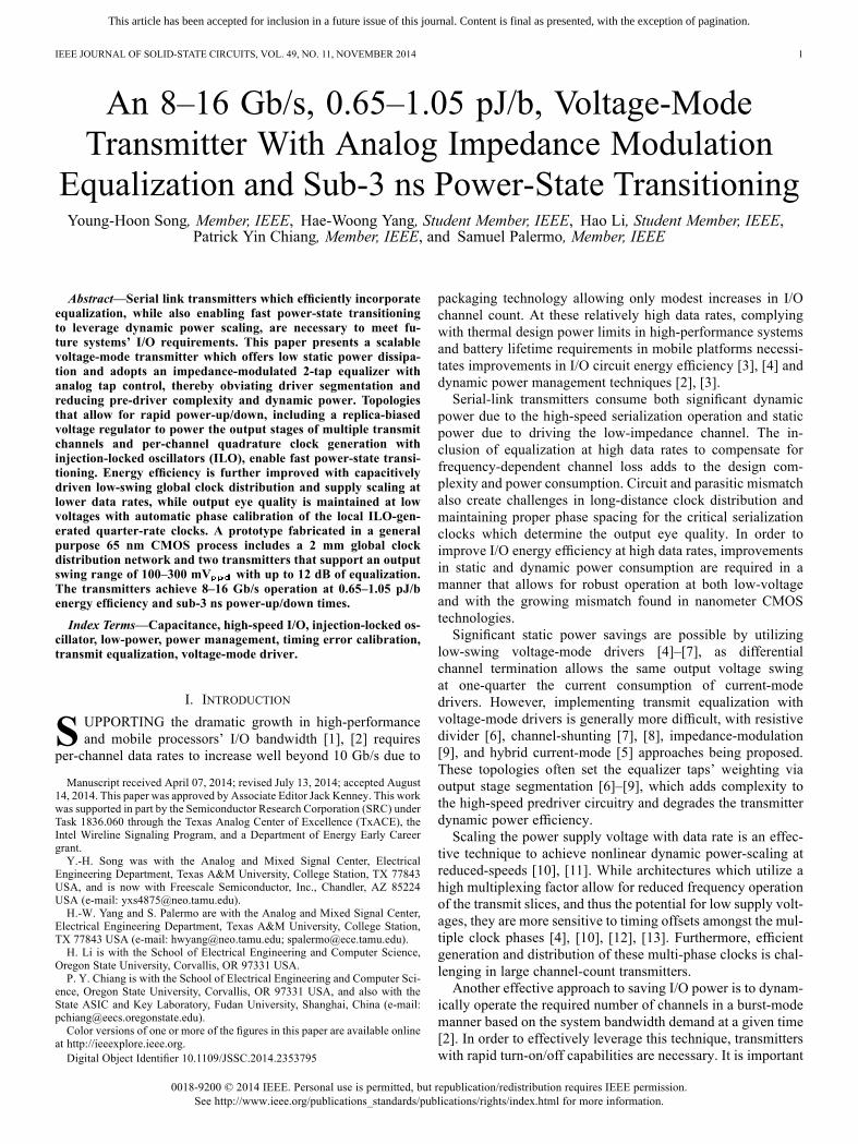
Fig. 1. Multi-channel serial-link transmitter architecture with dynamic powermanagement.
to quickly disable both switching and static power, which canbe particularly challenging with voltage-mode drivers due tooutput-stage regulator decoupling capacitance.This paper presents a scalable high-data-rate transmitter
architecture that allows for low overall power consumption in amanner that allows for dynamic power management to optimizesystem performance for varying workload demands. Section IIreviews key low-power design techniques employed in thisdesign, including capacitively driven wires for long-distanceclock distribution [14] and impedance-modulation equalization[9]. An overview of the proposed multi-channel transmitterarchitecture, which is able to maintain low-swing quarter-rateclocking through the global distribution and local multi-phasegeneration, is given in Section III. Section IV discussesthe power/data rate scalable transmitter channel design whichadopts an impedance-modulated 2-tap equalizer with analog tapcontrol, employs automatic phase calibration for low-voltageoperation, and utilizes a replica-biased voltage regulator toenable fast power-state transitioning. Experimental resultsfrom a GP 65 nm CMOS prototype are presented in Section V.Finally, Section VI concludes the paper.
II. LOW-POWER TRANSMITTER DESIGN TECHNIQUES
A typical low-power multi-channel serial-link transmitterarchitecture is shown in Fig. 1. In order to amortize clockingpower, the output of a global clock generation circuit, such asa phase-locked loop (PLL), is distributed to all of the transmitchannels. Here efficient global clock distribution techniques,such as low-swing CML signaling [11], [15], are often em-ployed in high channel count systems which span several mm.Each transmit channel performs parallel data serialization,implements equalization to compensate for frequency-depen-dent channel loss, and allows for dynamic power management(DPM) with rapid turn-on/off capabilities. This section reviewskey low-power design techniques employed in this design,including capacitively driven wires for long-distance clockdistribution [14] and impedance-modulation equalization [9],with further improvements offered in Sections III and IV.
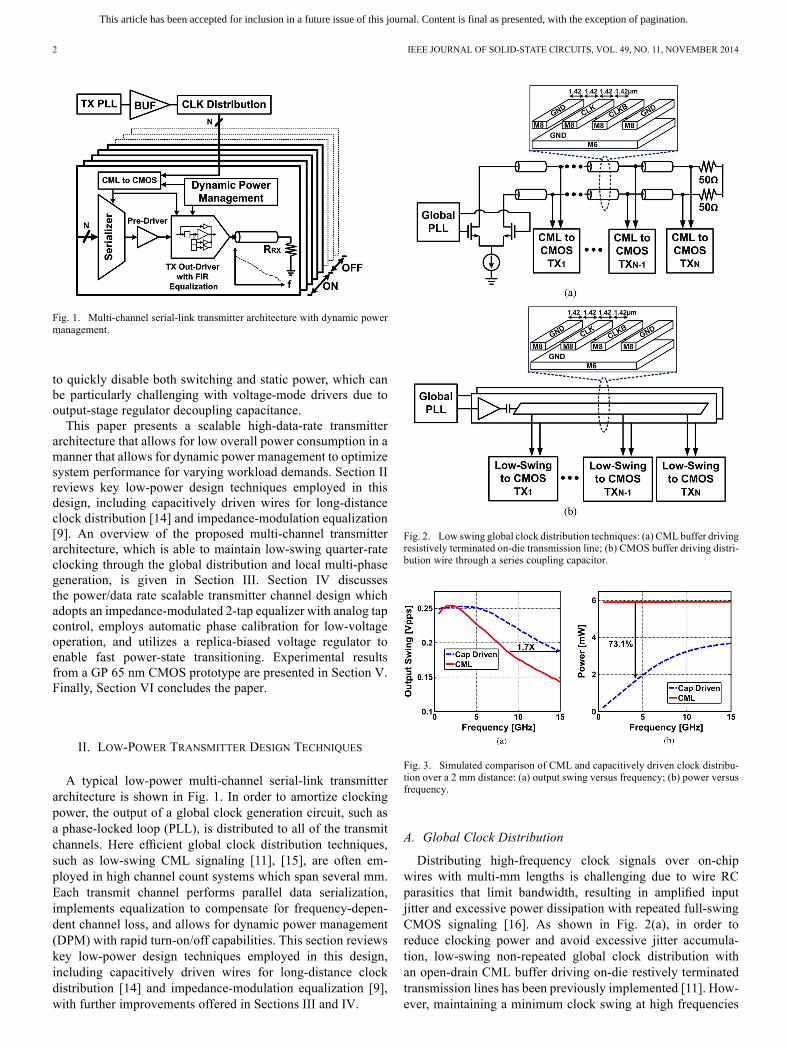
Fig. 2. Low swing global clock distribution techniques: (a) CML buffer drivingresistively terminated on-die transmission line; (b) CMOS buffer driving distri-bution wire through a series coupling capacitor.
Fig. 3. Simulated comparison of CML and capacitively driven clock distribu-tion over a 2 mm distance: (a) output swing versus frequency; (b) power versusfrequency.
A. Global Clock Distribution
Distributing high-frequency clock signals over on-chipwires with multi-mm lengths is challenging due to wire RCparasitics that limit bandwidth, resulting in amplified inputjitter and excessive power dissipation with repeated full-swingCMOS signaling [16]. As shown in Fig. 2(a), in order toreduce clocking power and avoid excessive jitter accumula-tion, low-swing non-repeated global clock distribution withan open-drain CML buffer driving on-die restively terminatedtransmission lines has been previously implemented [11]. How-ever, maintaining a minimum clock swing at high frequencies
This article has been accepted for inclusion in a future issue of this journal. Content is final as presented, with the exception of pagination.
SONG et al.: AN 8–16 Gb/s, 0.65–1.05 pJ/b, VOLTAGE-MODE TRANSMITTER WITH ANALOG IMPEDANCE MODULATION EQUALIZATION 3
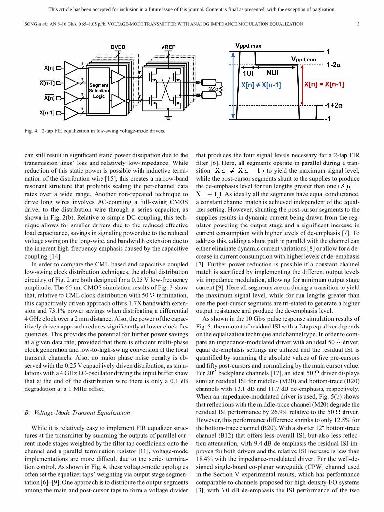
Fig. 4. 2-tap FIR equalization in low-swing voltage-mode drivers.
can still result in significant static power dissipation due to thetransmission lines’ loss and relatively low-impedance. Whilereduction of this static power is possible with inductive termi-nation of the distribution wire [15], this creates a narrow-bandresonant structure that prohibits scaling the per-channel datarates over a wide range. Another non-repeated technique todrive long wires involves AC-coupling a full-swing CMOSdriver to the distribution wire through a series capacitor, asshown in Fig. 2(b). Relative to simple DC-coupling, this tech-nique allows for smaller drivers due to the reduced effectiveload capacitance, savings in signaling power due to the reducedvoltage swing on the long-wire, and bandwidth extension due tothe inherent high-frequency emphasis caused by the capacitivecoupling [14].In order to compare the CML-based and capacitive-coupled
low-swing clock distribution techniques, the global distributioncircuitry of Fig. 2 are both designed for a 0.25 V low-frequencyamplitude. The 65 nm CMOS simulation results of Fig. 3 showthat, relative to CML clock distribution with 50 termination,this capacitively driven approach offers 1.7X bandwidth exten-sion and 73.1% power savings when distributing a differential4 GHz clock over a 2mm distance. Also, the power of the capac-itively driven approach reduces significantly at lower clock fre-quencies. This provides the potential for further power savingsat a given data rate, provided that there is efficient multi-phaseclock generation and low-to-high-swing conversion at the localtransmit channels. Also, no major phase noise penalty is ob-served with the 0.25 V capacitively driven distribution, as simu-lations with a 4 GHz LC-oscillator driving the input buffer showthat at the end of the distribution wire there is only a 0.1 dBdegradation at a 1 MHz offset.
B. Voltage-Mode Transmit Equalization
While it is relatively easy to implement FIR equalizer struc-tures at the transmitter by summing the outputs of parallel cur-rent-mode stages weighted by the filter tap coefficients onto thechannel and a parallel termination resistor [11], voltage-modeimplementations are more difficult due to the series termina-tion control. As shown in Fig. 4, these voltage-mode topologiesoften set the equalizer taps’ weighting via output stage segmen-tation [6]–[9]. One approach is to distribute the output segmentsamong the main and post-cursor taps to form a voltage divider
that produces the four signal levels necessary for a 2-tap FIRfilter [6]. Here, all segments operate in parallel during a tran-sition to yield the maximum signal level,while the post-cursor segments shunt to the supplies to producethe de-emphasis level for run lengths greater than one
. As ideally all the segments have equal conductance,a constant channel match is achieved independent of the equal-izer setting. However, shunting the post-cursor segments to thesupplies results in dynamic current being drawn from the reg-ulator powering the output stage and a significant increase incurrent consumption with higher levels of de-emphasis [7]. Toaddress this, adding a shunt path in parallel with the channel caneither eliminate dynamic current variations [8] or allow for a de-crease in current consumption with higher levels of de-emphasis[7]. Further power reduction is possible if a constant channelmatch is sacrificed by implementing the different output levelsvia impedance modulation, allowing for minimum output stagecurrent [9]. Here all segments are on during a transition to yieldthe maximum signal level, while for run lengths greater thanone the post-cursor segments are tri-stated to generate a higheroutput resistance and produce the de-emphasis level.As shown in the 10 Gb/s pulse response simulation results of
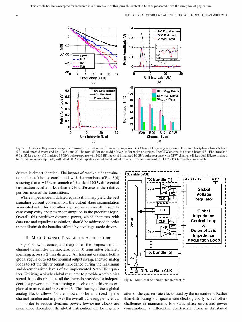
Fig. 5, the amount of residual ISI with a 2-tap equalizer dependson the equalization technique and channel type. In order to com-pare an impedance-modulated driver with an ideal 50 driver,equal de-emphasis settings are utilized and the residual ISI isquantified by summing the absolute values of five pre-cursorsand fifty post-cursors and normalizing by the main cursor value.For 20 backplane channels [17], an ideal 50 driver displayssimilar residual ISI for middle- (M20) and bottom-trace (B20)channels with 13.1 dB and 11.7 dB de-emphasis, respectively.When an impedance-modulated driver is used, Fig. 5(b) showsthat reflections with themiddle-trace channel (M20) degrade theresidual ISI performance by 26.9% relative to the 50 driver.However, this performance difference shrinks to only 12.8% forthe bottom-trace channel (B20).With a shorter 12 bottom-tracechannel (B12) that offers less overall ISI, but also less reflec-tion attenuation, with 9.4 dB de-emphasis the residual ISI im-proves for both drivers and the relative ISI increase is less than18.4% with the impedance-modulated driver. For the well-de-signed single-board co-planar waveguide (CPW) channel usedin the Section V experimental results, which has performancecomparable to channels proposed for high-density I/O systems[3], with 6.0 dB de-emphasis the ISI performance of the two
This article has been accepted for inclusion in a future issue of this journal. Content is final as presented, with the exception of pagination.
4 IEEE JOURNAL OF SOLID-STATE CIRCUITS, VOL. 49, NO. 11, NOVEMBER 2014
Fig. 5. 10 Gb/s voltage-mode 2-tap FIR transmit equalization performance comparison. (a) Channel frequency responses. The three backplane channels have5.2 total linecard traces and 12 (B12), and 20 bottom- (B20) and middle-layer (M20) backplane traces. The CPW channel is a single-board 5.8 FR4 trace and0.6 m SMA cable. (b) Simulated 10 Gb/s pulse response with M20 BP trace. (c) Simulated 10 Gb/s pulse response with CPW channel. (d) Residual ISI, normalizedto the main-cursor amplitude, with ideal 50 and impedance-modulated output drivers. Error bars account for 15% RX termination mismatch.
drivers is almost identical. The impact of receive-side termina-tion mismatch is also considered, with the error bars of Fig. 5(d)showing that a 15% mismatch of the ideal 100 differentialtermination results in less than a 2% difference in the relativeperformance of the transmitters.While impedance-modulated equalization may yield the best
signaling current consumption, the output stage segmentationassociated with this and other approaches can result in signifi-cant complexity and power consumption in the predriver logic.Overall, this predriver dynamic power, which increases withdata rate and equalizer resolution, should be addressed in orderto not diminish the benefits offered by a voltage-mode driver.
III. MULTI-CHANNEL TRANSMITTER ARCHITECTURE
Fig. 6 shows a conceptual diagram of the proposed multi-channel transmitter architecture, with 10 transmitter channelsspanning across a 2 mm distance. All transmitters share both aglobal regulator to set the nominal output swing, and two analogloops to set the driver output impedance during the maximumand de-emphasized levels of the implemented 2-tap FIR equal-izer. Utilizing a single global regulator to provide a stable biassignal that is distributed to all the channels provides for indepen-dent fast power-state transitioning of each output driver, as ex-plained in more detail in Section IV. The sharing of these globalanalog blocks allows for their power to be amortized by thechannel number and improves the overall I/O energy efficiency.In order to reduce dynamic power, low-swing clocks are
maintained throughout the global distribution and local gener-
Fig. 6. Multi-channel transmitter architecture.
ation of the quarter-rate clocks used by the transmitters. Ratherthan distributing four quarter-rate clocks globally, which offerschallenges in maintaining low static phase errors and powerconsumption, a differential quarter-rate clock is distributed
This article has been accepted for inclusion in a future issue of this journal. Content is final as presented, with the exception of pagination.
SONG et al.: AN 8–16 Gb/s, 0.65–1.05 pJ/b, VOLTAGE-MODE TRANSMITTER WITH ANALOG IMPEDANCE MODULATION EQUALIZATION 5
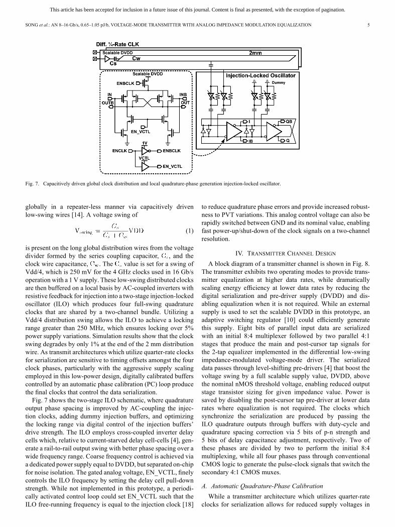
Fig. 7. Capacitively driven global clock distribution and local quadrature-phase generation injection-locked oscillator.
globally in a repeater-less manner via capacitively drivenlow-swing wires [14]. A voltage swing of
(1)
is present on the long global distribution wires from the voltagedivider formed by the series coupling capacitor, , and theclock wire capacitance, . The value is set for a swing ofVdd/4, which is 250 mV for the 4 GHz clocks used in 16 Gb/soperation with a 1 V supply. These low-swing distributed clocksare then buffered on a local basis by AC-coupled inverters withresistive feedback for injection into a two-stage injection-lockedoscillator (ILO) which produces four full-swing quadratureclocks that are shared by a two-channel bundle. Utilizing aVdd/4 distribution swing allows the ILO to achieve a lockingrange greater than 250 MHz, which ensures locking over 5%power supply variations. Simulation results show that the clockswing degrades by only 1% at the end of the 2 mm distributionwire. As transmit architectures which utilize quarter-rate clocksfor serialization are sensitive to timing offsets amongst the fourclock phases, particularly with the aggressive supply scalingemployed in this low-power design, digitally calibrated bufferscontrolled by an automatic phase calibration (PC) loop producethe final clocks that control the data serialization.Fig. 7 shows the two-stage ILO schematic, where quadrature
output phase spacing is improved by AC-coupling the injec-tion clocks, adding dummy injection buffers, and optimizingthe locking range via digital control of the injection buffers’drive strength. The ILO employs cross-coupled inverter delaycells which, relative to current-starved delay cell-cells [4], gen-erate a rail-to-rail output swing with better phase spacing over awide frequency range. Coarse frequency control is achieved viaa dedicated power supply equal to DVDD, but separated on-chipfor noise isolation. The gated analog voltage, EN_VCTL, finelycontrols the ILO frequency by setting the delay cell pull-downstrength. While not implemented in this prototype, a periodi-cally activated control loop could set EN_VCTL such that theILO free-running frequency is equal to the injection clock [18]
to reduce quadrature phase errors and provide increased robust-ness to PVT variations. This analog control voltage can also berapidly switched between GND and its nominal value, enablingfast power-up/shut-down of the clock signals on a two-channelresolution.
IV. TRANSMITTER CHANNEL DESIGN
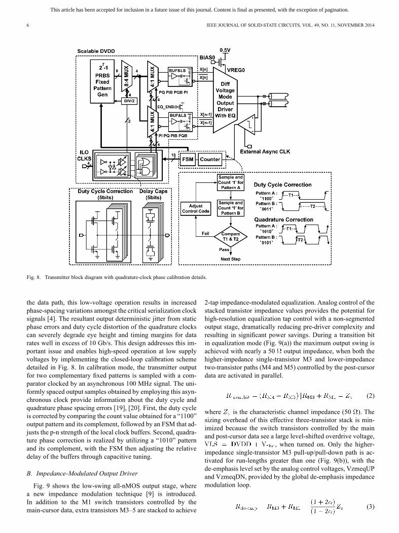
A block diagram of a transmitter channel is shown in Fig. 8.The transmitter exhibits two operating modes to provide trans-mitter equalization at higher data rates, while dramaticallyscaling energy efficiency at lower data rates by reducing thedigital serialization and pre-driver supply (DVDD) and dis-abling equalization when it is not required. While an externalsupply is used to set the scalable DVDD in this prototype, anadaptive switching regulator [10] could efficiently generatethis supply. Eight bits of parallel input data are serializedwith an initial 8:4 multiplexer followed by two parallel 4:1stages that produce the main and post-cursor tap signals forthe 2-tap equalizer implemented in the differential low-swingimpedance-modulated voltage-mode driver. The serializeddata passes through level-shifting pre-drivers [4] that boost thevoltage swing by a full scalable supply value, DVDD, abovethe nominal nMOS threshold voltage, enabling reduced outputstage transistor sizing for given impedance value. Power issaved by disabling the post-cursor tap pre-driver at lower datarates where equalization is not required. The clocks whichsynchronize the serialization are produced by passing theILO quadrature outputs through buffers with duty-cycle andquadrature spacing correction via 5 bits of p-n strength and5 bits of delay capacitance adjustment, respectively. Two ofthese phases are divided by two to perform the initial 8:4multiplexing, while all four phases pass through conventionalCMOS logic to generate the pulse-clock signals that switch thesecondary 4:1 CMOS muxes.
A. Automatic Quadrature-Phase Calibration
While a transmitter architecture which utilizes quarter-rateclocks for serialization allows for reduced supply voltages in
This article has been accepted for inclusion in a future issue of this journal. Content is final as presented, with the exception of pagination.
6 IEEE JOURNAL OF SOLID-STATE CIRCUITS, VOL. 49, NO. 11, NOVEMBER 2014
Fig. 8. Transmitter block diagram with quadrature-clock phase calibration details.
the data path, this low-voltage operation results in increasedphase-spacing variations amongst the critical serialization clocksignals [4]. The resultant output deterministic jitter from staticphase errors and duty cycle distortion of the quadrature clockscan severely degrade eye height and timing margins for datarates well in excess of 10 Gb/s. This design addresses this im-portant issue and enables high-speed operation at low supplyvoltages by implementing the closed-loop calibration schemedetailed in Fig. 8. In calibration mode, the transmitter outputfor two complementary fixed patterns is sampled with a com-parator clocked by an asynchronous 100 MHz signal. The uni-formly spaced output samples obtained by employing this asyn-chronous clock provide information about the duty cycle andquadrature phase spacing errors [19], [20]. First, the duty cycleis corrected by comparing the count value obtained for a “1100”output pattern and its complement, followed by an FSM that ad-justs the p-n strength of the local clock buffers. Second, quadra-ture phase correction is realized by utilizing a “1010” patternand its complement, with the FSM then adjusting the relativedelay of the buffers through capacitive tuning.
B. Impedance-Modulated Output Driver
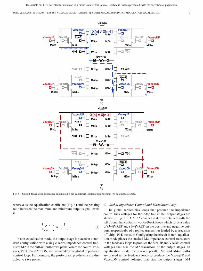
Fig. 9 shows the low-swing all-nMOS output stage, wherea new impedance modulation technique [9] is introduced.In addition to the M1 switch transistors controlled by themain-cursor data, extra transistors M3–5 are stacked to achieve
2-tap impedance-modulated equalization. Analog control of thestacked transistor impedance values provides the potential forhigh-resolution equalization tap control with a non-segmentedoutput stage, dramatically reducing pre-driver complexity andresulting in significant power savings. During a transition bitin equalization mode (Fig. 9(a)) the maximum output swing isachieved with nearly a 50 output impedance, when both thehigher-impedance single-transistor M3 and lower-impedancetwo-transistor paths (M4 and M5) controlled by the post-cursordata are activated in parallel.
(2)
where is the characteristic channel impedance (50 ). Thesizing overhead of this effective three-transistor stack is min-imized because the switch transistors controlled by the mainand post-cursor data see a large level-shifted overdrive voltage,
, when turned on. Only the higher-impedance single-transistor M3 pull-up/pull-down path is ac-tivated for run-lengths greater than one (Fig. 9(b)), with thede-emphasis level set by the analog control voltages, VzmeqUPand VzmeqDN, provided by the global de-emphasis impedancemodulation loop.
(3)
This article has been accepted for inclusion in a future issue of this journal. Content is final as presented, with the exception of pagination.
SONG et al.: AN 8–16 Gb/s, 0.65–1.05 pJ/b, VOLTAGE-MODE TRANSMITTER WITH ANALOG IMPEDANCE MODULATION EQUALIZATION 7
Fig. 9. Output driver with impedance-modulated 2-tap equalizer: (a) transition-bit state; (b) de-emphasis state.
where is the equalization coefficient (Fig. 4) and the peakingratio between the maximum and minimum output signal levelsis
(4)
In non-equalization mode, the output stage is placed in a stan-dard configuration with a single series impedance-control tran-sistorM2 in the pull-up/pull-down paths, where the control volt-ages, VzcUP and VzcDN, are provided by the global impedancecontrol loop. Furthermore, the post-cursor pre-drivers are dis-abled to save power.
C. Global Impedance Control and Modulation Loop
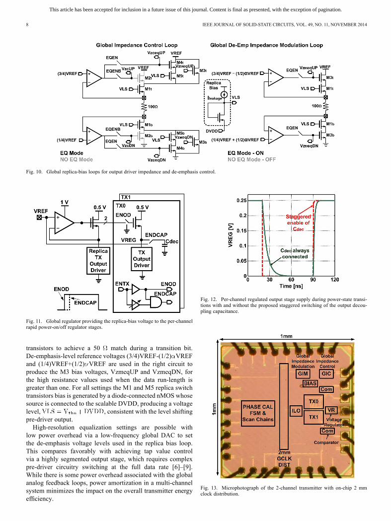
The global replica-bias loops that produce the impedancecontrol bias voltages for the 2-tap transmitter output stages areshown in Fig. 10. A 50 channel match is obtained with theleft circuit that contains two feedback loops which force a valueof (3/4)VREF and (1/4)VREF on the positive and negative out-puts, respectively, of a replica transmitter loaded by a precisionoff-chip 100 resistor. Configuring the circuit in non-equaliza-tion mode places the stacked M2 impedance control transistorsin the feedback loops to produce the VzcUP and VzcDN controlvoltages that bias the M2 transistors of the output stages. Inequalization mode, the stacked parallel M3 and M4–5 pathsare placed in the feedback loops to produce the VzceqUP andVzceqDN control voltages that bias the output stages’ M4
This article has been accepted for inclusion in a future issue of this journal. Content is final as presented, with the exception of pagination.
8 IEEE JOURNAL OF SOLID-STATE CIRCUITS, VOL. 49, NO. 11, NOVEMBER 2014
Fig. 10. Global replica-bias loops for output driver impedance and de-emphasis control.
Fig. 11. Global regulator providing the replica-bias voltage to the per-channelrapid power-on/off regulator stages.
transistors to achieve a 50 match during a transition bit.De-emphasis-level reference voltages (3/4)VREF-(1/2) VREFand (1/4)VREF+(1/2) VREF are used in the right circuit toproduce the M3 bias voltages, VzmeqUP and VzmeqDN, forthe high resistance values used when the data run-length isgreater than one. For all settings the M1 and M5 replica switchtransistors bias is generated by a diode-connected nMOS whosesource is connected to the scalable DVDD, producing a voltagelevel, , consistent with the level shiftingpre-driver output.High-resolution equalization settings are possible with
low power overhead via a low-frequency global DAC to setthe de-emphasis voltage levels used in the replica bias loop.This compares favorably with achieving tap value controlvia a highly segmented output stage, which requires complexpre-driver circuitry switching at the full data rate [6]–[9].While there is some power overhead associated with the globalanalog feedback loops, power amortization in a multi-channelsystem minimizes the impact on the overall transmitter energyefficiency.
Fig. 12. Per-channel regulated output stage supply during power-state transi-tions with and without the proposed staggered switching of the output decou-pling capacitance.
Fig. 13. Microphotograph of the 2-channel transmitter with on-chip 2 mmclock distribution.
This article has been accepted for inclusion in a future issue of this journal. Content is final as presented, with the exception of pagination.
SONG et al.: AN 8–16 Gb/s, 0.65–1.05 pJ/b, VOLTAGE-MODE TRANSMITTER WITH ANALOG IMPEDANCE MODULATION EQUALIZATION 9
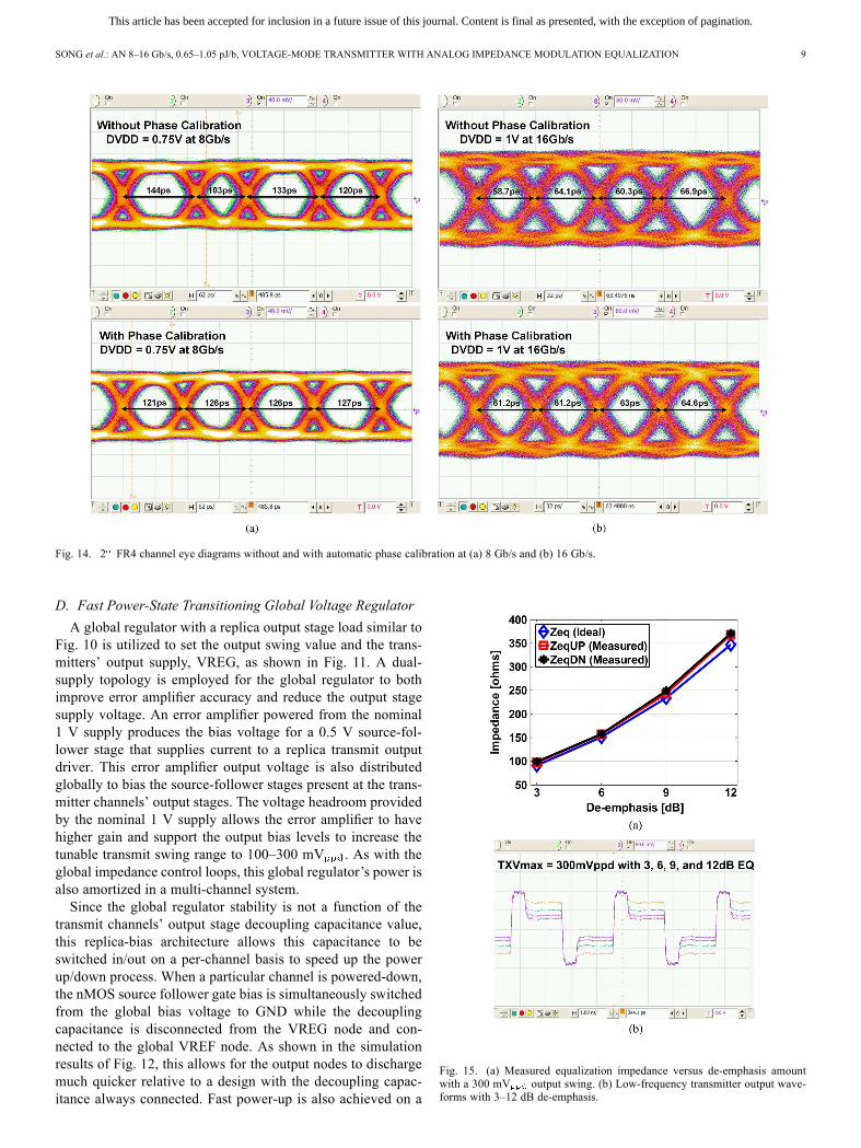
Fig. 14. 2 FR4 channel eye diagrams without and with automatic phase calibration at (a) 8 Gb/s and (b) 16 Gb/s.
D. Fast Power-State Transitioning Global Voltage Regulator
A global regulator with a replica output stage load similar toFig. 10 is utilized to set the output swing value and the trans-mitters’ output supply, VREG, as shown in Fig. 11. A dual-supply topology is employed for the global regulator to bothimprove error amplifier accuracy and reduce the output stagesupply voltage. An error amplifier powered from the nominal1 V supply produces the bias voltage for a 0.5 V source-fol-lower stage that supplies current to a replica transmit outputdriver. This error amplifier output voltage is also distributedglobally to bias the source-follower stages present at the trans-mitter channels’ output stages. The voltage headroom providedby the nominal 1 V supply allows the error amplifier to havehigher gain and support the output bias levels to increase thetunable transmit swing range to 100–300 mV . As with theglobal impedance control loops, this global regulator’s power isalso amortized in a multi-channel system.Since the global regulator stability is not a function of the
transmit channels’ output stage decoupling capacitance value,this replica-bias architecture allows this capacitance to beswitched in/out on a per-channel basis to speed up the powerup/down process. When a particular channel is powered-down,the nMOS source follower gate bias is simultaneously switchedfrom the global bias voltage to GND while the decouplingcapacitance is disconnected from the VREG node and con-nected to the global VREF node. As shown in the simulationresults of Fig. 12, this allows for the output nodes to dischargemuch quicker relative to a design with the decoupling capac-itance always connected. Fast power-up is also achieved on a
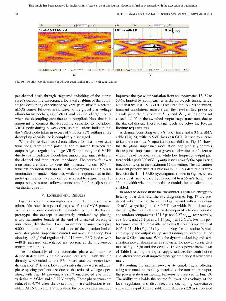
Fig. 15. (a) Measured equalization impedance versus de-emphasis amountwith a 300 mV output swing. (b) Low-frequency transmitter output wave-forms with 3–12 dB de-emphasis.
This article has been accepted for inclusion in a future issue of this journal. Content is final as presented, with the exception of pagination.
10 IEEE JOURNAL OF SOLID-STATE CIRCUITS, VOL. 49, NO. 11, NOVEMBER 2014
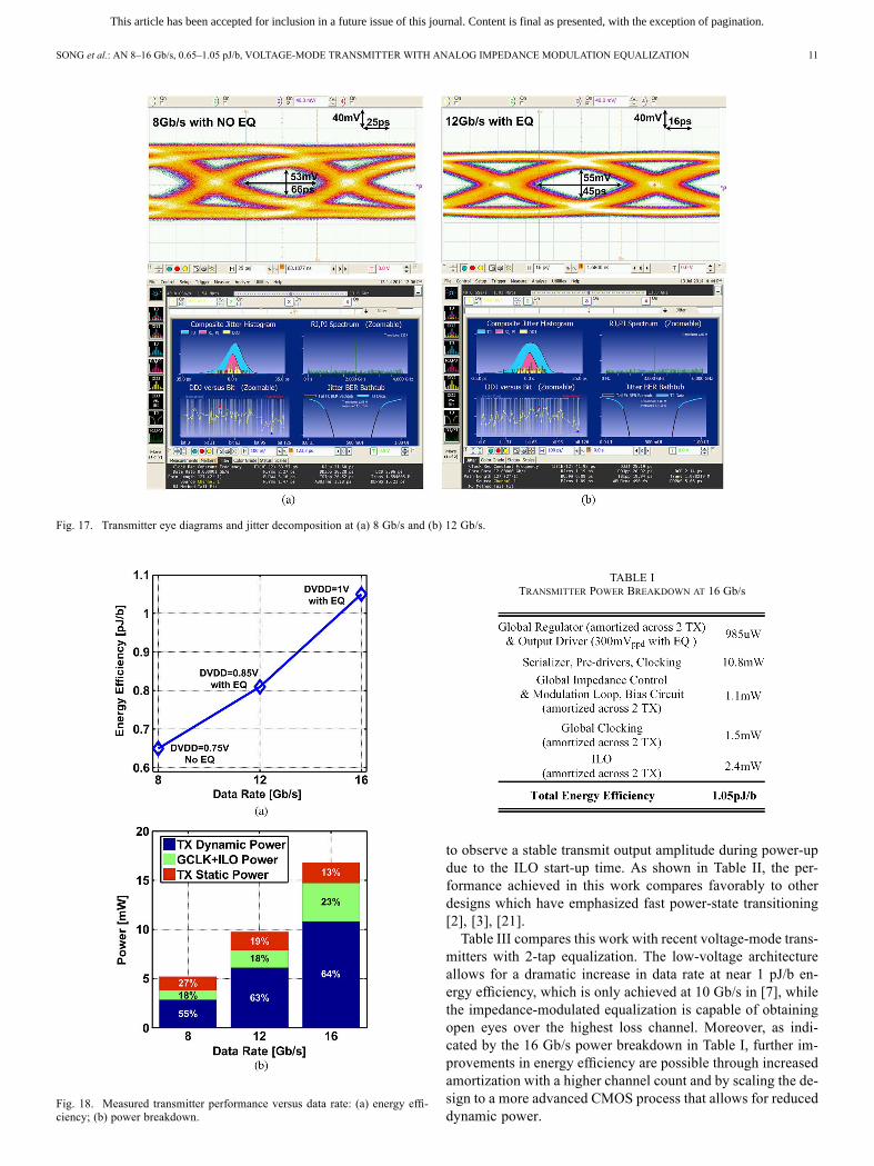
Fig. 16. 16 Gb/s eye diagrams: (a) without equalization and (b) with equalization.
per-channel basis through staggered switching of the outputstage’s decoupling capacitance. Delayed enabling of the outputstage’s decoupling capacitance by 550 ps relative to when thenMOS source follower is switched to the global bias voltageallows for faster charging of VREG and minimal charge sharingwhen the decoupling capacitance is reapplied. Note that it isimportant to connect the decoupling capacitor to the globalVREF node during power-down, as simulations indicate thatthe VREG node takes in excess of 7 ns for 95% settling if thedecoupling capacitance is completely discharged.While this replica-bias scheme allows for fast power-state
transitions, there is the potential for mismatch between theoutput stages’ regulated voltage VREG and the global VREFdue to the impedance modulation amount and mismatches inthe channel and termination impedance. The source followertransistors are sized to keep this mismatch under 10% intransient operation with up to 12 dB de-emphasis and 5% RXtermination mismatch. Note that, while not implemented in thisprototype, higher accuracy can be achieved by segmenting theoutput stages’ source follower transistors for fine adjustmentvia digital control.
V. EXPERIMENTAL RESULTS
Fig. 13 shows a die microphotograph of the proposed trans-mitter, fabricated in a general purpose 65 nm CMOS process.While chip area constraints prevented a full 10-channelprototype, the concept is accurately emulated by placinga two-transmitter bundle at the end of a snaked on-chip 2mm clock distribution. Each transmitter channel occupies0.006 mm , and the combined area of the injection-lockedoscillator, global impedance control and modulation loop, biascircuitry, and global regulator is 0.014 mm . ESD diodes with40 fF parasitic capacitance are present at the high-speed
transmitter outputs.The functionality of the automatic phase calibration is
demonstrated with a chip-on-board test setup, with the diedirectly wirebonded to the FR4 board and the transmittersdriving short 2 traces. Lower data rates display worse inherentphase spacing performance due to the reduced voltage oper-ation, with Fig. 14 showing a 28.5% uncorrected eye widthvariation at 8 Gb/s and a 0.75 V supply. These phase errors arereduced to 4.7% when the closed-loop phase calibration is en-abled. At 16 Gb/s and 1 V operation, the phase calibration loop
improves the eye width variation from an uncorrected 13.1% to5.4%, limited by nonlinearities in the duty-cycle tuning range.Note that while a 1 V DVDD is required for 16 Gb/s operation,transient simulations indicate that the level-shifted pre-drivesignals generate a maximum and which does notexceed 1.1 V in the switched output stage transistors due tothe stacked design. These voltage levels are below the 10-yearlifetime requirements.A channel consisting of a 5.8 FR4 trace and a 0.6 m SMA
cable (Fig. 5), with 15.5 dB loss at 8 GHz, is used to charac-terize the transmitter’s equalization capabilities. Fig. 15 showsthat the global impedance modulation loop precisely controlsthe required impedance for a given equalization coefficient towithin 7% of the ideal value, while low-frequency output pat-terns with a peak 300mV output swing verify the equalizer’sfunctionality up to the maximum 12 dB setting. The transmittertransient performance at a maximum 16 Gb/s data rate is veri-fied with the PRBS eye diagrams shown in Fig. 16, wherea previously near-closed eye is opened to a 55 mV height and33.4 ps width when the impedance-modulation equalization isenabled.In order to demonstrate the transmitter’s scalable energy ef-
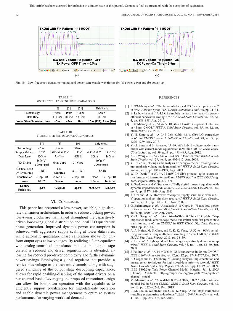
ficiency over data rate, the eye diagrams of Fig. 17 are pro-duced with the same channel as Fig. 16 and with a minimum50 mV eye height and 0.5UI eye width. From these eyediagrams, the total jitter can be decomposed into deterministicand random components of 31.6 ps and 2.27 ps , respectively,at 8 Gb/s, and 25.2 ps and 1.19 ps at 12 Gb/s. For this per-formance level the transmitter achieves 8–16 Gb/s operation at0.65–1.05 pJ/b (Fig. 18) by optimizing the transmitter’s scal-able supply and output swing and disabling equalization at thelowest 8 Gb/s data rate. While the dynamic clocking and seri-alization power dominates, as shown in the power versus datarate of Fig. 18(b) and the detailed 16 Gb/s power breakdownof Table I, scaling the digital supply reduces this contributionand allows for overall improved energy efficiency at lower datarates.By routing the internal power-state enable signal off-chip
using a channel that is delay-matched to the transmitter output,the power-state transitioning behavior is observed in Fig. 19.The ability to disable the source-follower bias voltage of thelocal regulators and disconnect the decoupling capacitanceallow for a rapid 0.5 ns disable time. A longer 2.9 ns is required
This article has been accepted for inclusion in a future issue of this journal. Content is final as presented, with the exception of pagination.
SONG et al.: AN 8–16 Gb/s, 0.65–1.05 pJ/b, VOLTAGE-MODE TRANSMITTER WITH ANALOG IMPEDANCE MODULATION EQUALIZATION 11
Fig. 17. Transmitter eye diagrams and jitter decomposition at (a) 8 Gb/s and (b) 12 Gb/s.
Fig. 18. Measured transmitter performance versus data rate: (a) energy effi-ciency; (b) power breakdown.
TABLE ITRANSMITTER POWER BREAKDOWN AT 16 Gb/s
to observe a stable transmit output amplitude during power-updue to the ILO start-up time. As shown in Table II, the per-formance achieved in this work compares favorably to otherdesigns which have emphasized fast power-state transitioning[2], [3], [21].Table III compares this work with recent voltage-mode trans-
mitters with 2-tap equalization. The low-voltage architectureallows for a dramatic increase in data rate at near 1 pJ/b en-ergy efficiency, which is only achieved at 10 Gb/s in [7], whilethe impedance-modulated equalization is capable of obtainingopen eyes over the highest loss channel. Moreover, as indi-cated by the 16 Gb/s power breakdown in Table I, further im-provements in energy efficiency are possible through increasedamortization with a higher channel count and by scaling the de-sign to a more advanced CMOS process that allows for reduceddynamic power.
This article has been accepted for inclusion in a future issue of this journal. Content is final as presented, with the exception of pagination.
12 IEEE JOURNAL OF SOLID-STATE CIRCUITS, VOL. 49, NO. 11, NOVEMBER 2014
Fig. 19. Low-frequency transmitter output and power-state enable waveforms for (a) power-down and (b) power-up.
TABLE IIPOWER STATE TRANSIENT TIME COMPARISONS
TABLE IIITRANSMITTER PERFORMANCE COMPARISONS
VI. CONCLUSION
This paper has presented a low-power, scalable, high-data-rate transmitter architecture. In order to reduce clocking power,low-swing clocks are maintained throughout the capacitivelydriven low-swing global distribution and local ILO quadraturephase generation. Improved dynamic power consumption isachieved with aggressive supply scaling at lower data rates,while automatic quadrature phase calibration allows for uni-form output eyes at low voltages. By realizing a 2-tap equalizerwith analog-controlled impedance modulation, output stagecurrent is reduced and driver segmentation is obviated, al-lowing for reduced pre-driver complexity and further dynamicpower savings. Employing a global regulator that provides areplica-bias voltage to the transmit channels, along with stag-gered switching of the output stage decoupling capacitance,allows for rapid enabling/disabling of the output drivers on aper-channel basis. Leveraging the proposed transmitter designcan allow for low-power operation with the capabilities toefficiently support equalization for high-data-rate operationand enable dynamic power management to optimize systemperformance for varying workload demands.
REFERENCES
[1] F. O’Mahony et al., “The future of electrical I/O for microprocessors,”in Proc. 2009 Int. Symp. VLSI Design, Automation and Test, pp. 31–34.
[2] B. Leibowitz et al., “A 4.3 GB/s mobile memory interface with power-efficient bandwidth scaling,” IEEE J. Solid-State Circuits, vol. 45, no.4, pp. 889–898, Apr. 2010.
[3] F. O’Mahony et al., “A 47 10 Gb/s 1.4 mW/Gb/s parallel interfacein 45 nm CMOS,” IEEE J. Solid-State Circuits, vol. 45, no. 12, pp.2828–2837, Dec. 2010.
[4] Y.-H. Song et al., “A 0.47–0.66 pJ/bit, 4.8–8 Gb/s I/O transceiverin 65 nm CMOS,” IEEE J. Solid-State Circuits, vol. 48, no. 5, pp.1276–1289, May 2013.
[5] Y.-H. Song and S. Palermo, “A 6-Gbit/s hybrid voltage-mode trans-mitter with current-mode equalization in 90-nm CMOS,” IEEE Trans.Circuits Syst. II, vol. 59, no. 8, pp. 491–495, Aug. 2012.
[6] K.-L. Wong et al., “A 27-mW 3.6-Gb/s I/O transceiver,” IEEE J. Solid-State Circuits, vol. 39, no. 4, pp. 602–612, Apr. 2004.
[7] Y. Lu et al., “Design and analysis of energy-efficient reconfigurablepre-emphasis voltage-mode transmitter,” IEEE J. Solid-State Circuits,vol. 48, no. 8, pp. 1898–1909, Aug. 2013.
[8] W. D. Dettloff et al., “A 32 mW 7.4 Gb/s protocol-agile source-se-ries terminated transmitter in 45 nm CMOS SOI,” in IEEE ISSCC Dig.Tech. Papers, 2010, pp. 370–371.
[9] R. Sredojevic and V. Stojanovic, “Fully digital transmit equalizer withdynamic impedance modulation,” IEEE J. Solid-State Circuits, vol. 46,no. 8, pp. 1857–1869, Aug. 2011.
[10] J. Kim and M. A. Horowitz, “Adaptive supply serial links with sub-1V operation and per-pin clock recovery,” IEEE J. Solid-State Circuits,vol. 37, no. 11, pp. 1403–1413, Nov. 2002.
[11] G. Balamurugan et al., “A scalable 5–15 Gbps, 14–75 mW low powerI/O transceiver in 65 nm CMOS,” IEEE J. Solid-State Circuits, vol. 43,no. 4, pp. 1010–1019, Apr. 2008.
[12] Y.-H. Song et al., “An 8-to-16Gb/s 0.65-to-1.05 pJ/b 2-tapimpedance-modulated voltage-mode transmitter with fast power-statetransitioning in 65 nm CMOS,” in IEEE ISSCC Dig. Tech. Papers,2014, pp. 446–447.
[13] A. A. Hafez, M.-S. Chen, and C.-K. K. Yang, “A 32-to-48Gb/s serial-izing transmitter using multiphase sampling in 65 nm CMOS,” in IEEEISSCC Dig. Tech. Papers, 2013, pp. 38–39.
[14] R. Ho et al., “High speed and low energy capacitively driven on-chipwires,” IEEE J. Solid-State Circuits, vol. 43, no. 1, pp. 52–60, Jan.2008.
[15] J. Poulton et al., “A 14-mW 6.25-Gb/s transceiver in 90-nm CMOS,”IEEE J. Solid-State Circuits, vol. 42, no. 12, pp. 2745–2757, Dec. 2007.
[16] B. Casper and F. O’Mahony, “Clocking analysis, implementation andmeasurement techniques for high-speed data links—A tutorial,” IEEETrans. Circuits Syst. I, Reg. Papers, vol. 56, no. 1, pp. 17–39, Jan. 2009.
[17] IEEE P802.3ap Task Force Channel Model Material. Jul. 1, 2005[Online]. Available: http://grouper.ieee.org/groups/802/3/ap/public/channel_model
[18] M. Mansuri et al., “A scalable 0.128–1 Tb/s, 0.8–2.6 pJ/bit, 64-laneparallel I/O in 32 nm CMOS,” IEEE J. Solid-State Circuits, vol. 48,no. 12, pp. 3229–3242, Dec. 2013.
[19] L.-M. Lee, D. Weinlader, and C.-K. K. Yang, “A sub-10 ps multiphasesampling system using redundancy,” IEEE J. Solid-State Circuits, vol.41, no. 1, pp. 265–273, Jan. 2006.

This article has been accepted for inclusion in a future issue of this journal. Content is final as presented, with the exception of pagination.
SONG et al.: AN 8–16 Gb/s, 0.65–1.05 pJ/b, VOLTAGE-MODE TRANSMITTER WITH ANALOG IMPEDANCE MODULATION EQUALIZATION 13
[20] L. Xia et al., “Sub-2-ps, static phase error calibration technique in-corporating measurement uncertainty cancellation for multi-gigahertztime-interleaved T/H circuits,” IEEE Trans. Circuits Syst. I, Reg. Pa-pers, vol. 59, no. 2, pp. 276–284, Feb. 2012.
[21] J. Zerbe et al., “A 5.6 Gb/s 2.4 mW/Gb/s bidirectional link with 8 nspower-on,” in IEEE Symp. VLSI Circuits Dig., 2011, pp. 82–83.
Young-Hoon Song (M’14) received the B.S. andM.S. degrees in electrical engineering from theUniversity of Texas at Arlington, TX, USA, in 2002and 2004, respectively, and the Ph.D. degree inelectrical engineering from Texas A&M University,College Station, TX, USA, in 2014.In 2008 and 2012, he was an intern at Broadcom,
Irvine, CA, USA, and at IBM T. J. Watson ResearchCenter, Yorktown Heights, NY, USA. He is now withFreescale Semiconductor as a high-speed transceiverdesign engineer. His research interests include
mixed-signal integrated circuit design primarily as applied to power-efficientserial link transceivers for high-speed digital communications.
Hae-Woong Yang (S’13) received the B.S. andM.E. degrees in electrical and computer engineeringfrom Texas A&M University, College Station, TX,USA, in 2007 and 2009, respectively. He is currentlyworking toward the Ph.D. degree at the Analogand Mixed Signal Center (AMSC) of Texas A&MUniversity.His interests include low-power high-speed
electrical link circuits, clock generation circuits, andsignal integrity.
Hao Li (S’14) received the B.S. degree in microelec-tronics from Tsinghua University, Beijing, China, in2009, and the M.S. degree in computer architecturefrom the Institute of Computing Technology, ChineseAcademy of Sciences, Beijing, China, in 2012. Hehas been working towards the Ph.D. degree in elec-trical engineering at Oregon State University, Cor-vallis, OR, USA, since 2012.His current research interests include energy-ef-
ficient high-speed circuits for electrical and opticalI/O.
Patrick Yin Chiang (S’99–M’04) received theB.S. degree in electrical engineering and computersciences from the University of California, Berkeley,CA, USA, in 1998, and the M.S. and Ph.D. degreesin electrical engineering from Stanford University,Stanford, CA, USA, in 2001 and 2007.He is an Associate Professor (on sabbatical) at
Oregon State University, Corvallis, OR, USA. Hecurrently is a 1000-Talents Young Professor at theASIC and System State Key Laboratory at FudanUniversity, Shanghai, China. In 1998, he was a de-
sign engineer at Datapath Systems (now LSI), where he designed a low-power,standard cell library for xDSL. In 2003, he was a research intern at Velio Com-munications (now Rambus), investigating 10 GHz clock synthesis techniques.In 2004, he was a consultant at Telegent Systems (now Spreadtrum), where heanalyzed low-phase VCOs for TV tuners. In 2006, he was a visiting NSF Re-search Fellow at Tsinghua University, China, investigating super-regenerativeRF transceivers. His interests are in energy-efficient circuits and systems, suchas low-power wireline and photonic interfaces, energy-constrained medicalsensors, and reliable near-threshold computing.Dr. Chiang was a recipient of a 2010 Department of Energy Early Career
award and a 2012 NSF CAREER award. He is an associate editor of IEEETRANSACTIONS ON BIOMEDICAL CIRCUITS AND SYSTEMS, and is on the tech-nical program committee for the IEEE Custom Integrated Circuits Conference.
Samuel Palermo (S’98–M’07) received the B.S.and M.S. degrees in electrical engineering fromTexas A&M University, College Station, TX, USA,in 1997 and 1999, respectively, and the Ph.D. degreein electrical engineering from Stanford University,Stanford, CA, USA, in 2007.From 1999 to 2000, he was with Texas Instru-
ments, Dallas, TX, USA, where he worked onthe design of mixed-signal integrated circuits forhigh-speed serial data communication. From 2006 to2008, he was with Intel Corporation, Hillsboro, OR,
USA, where he worked on high-speed optical and electrical I/O architectures.In 2009, he joined the Electrical and Computer Engineering Department ofTexas A&M University, where he is currently an Assistant Professor. Hisresearch interests include high-speed electrical and optical links, clock recoverysystems, and techniques for device variability compensation.Dr. Palermo was a recipient of a 2013 NSF CAREER award. He is a
member of Eta Kappa Nu. He currently serves as an associate editor for IEEETRANSACTIONS ON CIRCUITS AND SYSTEMS II, and served on the IEEE CASBoard of Governors from 2011 to 2012. He received, as a coauthor, the JackRaper Award for Outstanding Technology Directions Paper at the 2009 IEEEInternational Solid-State Circuits Conference.