
IEEE JOURNAL OF SOLID-STATE CIRCUITS, VOL. 43, NO. 5, MAY …neil/zeynep/paper2.pdf ·...
16
IEEE JOURNAL OF SOLID-STATE CIRCUITS, VOL. 43, NO. 5, MAY 2008 1287 Efficient Far-Field Radio Frequency Energy Harvesting for Passively Powered Sensor Networks Triet Le, Karti Mayaram, Fellow, IEEE, and Terri Fiez, Fellow, IEEE Abstract—An RF-DC power conversion system is designed to ef- ficiently convert far-field RF energy to DC voltages at very low re- ceived power and voltages. Passive rectifier circuits are designed in a 0.25 m CMOS technology using floating gate transistors as rec- tifying diodes. The 36-stage rectifier can rectify input voltages as low as 50 mV with a voltage gain of 6.4 and operates with received power as low as 5.5 W( 22.6 dBm). Optimized for far field, the circuit operates at a distance of 44 m from a 4 W EIRP source. The high voltage range achieved at low load current make it ideal for use in passively powered sensor networks. Index Terms—Far field, floating gate, high efficiency, interface circuit, micro power, passively powered, power conversion, RF powered, rectifier, sensor network. I. INTRODUCTION P ASSIVELY powered devices are becoming increasingly important for a wide range of sensing applications. Also known as remotely powered devices, passively powered devices do not require any internal power source while extracting their power from propagating radio waves, sunlight, mechanical vi- bration [1], thermal gradients, convection flows or other forms of harvestable energy. One of the most popular power extrac- tion methods for passively powered devices is to harvest power from propagating radio frequency (RF) signals [2]. RF powered devices are often used in applications such as structural monitoring where the RF powered devices are em- bedded into a structure making battery replacement impossible without destroying the structure. Some applications employing RF powered devices require deployment of these devices in very large numbers thus, making individual node battery replacement impractical. RF powered devices are often part of telemetry systems to re- motely measure and report data back to a central processing unit [3]–[6]. Devices powered by propagating RF waves are most often used in passive radio frequency identification (RFID) or passive RF tags to replace the bar code as a new form of data collection [2], [7]. Passive RFID tags are typically used in the range of 1–3 meters. Many modern biomedical implants are pas- sively powered with radio waves to prolong the lifetime of the implanted device, and to reduce the chances of infection and chemical instability from the use of batteries [8], [9]. Bionic implants generally operate within close proximity of the base station (typically 1–50 cm) and must be robustly designed since Manuscript received June 25, 2007; revised January 28, 2008. This work was supported in part by the NSF under Grant DBI-05292230. The authors are with the School of Electrical Engineering and Computer Sci- ence, Oregon State University, Corvallis, OR 97331 USA (e-mail: trietl@gmail. com). Digital Object Identifier 10.1109/JSSC.2008.920318 there is little tolerance for error in implanted devices. RF pow- ered devices are also used in ultra-low-power sensor networks in remote areas to eliminate the use of batteries in the sensor system and to keep the sensor network free of maintenance [10], [11]. The applications for these sensor networks normally re- quire an operating distance of 3 to 100 meters and they usually have a backup battery in case the power provided by the RF radi- ation is insufficient. Other applications for RF powered devices include access control, equipment monitoring and even personal identification. In all of these applications, there must be a power conver- sion circuit that can extract enough DC power from the incident electromagnetic waves for the passive device to operate. Previ- ously reported far field RF powered devices generally operate from distances of less than 10 meter from the RF source due to the high power loss from RF wave propagation at UHF fre- quencies [12]. Others previous work achieved sufficient power but provides low output voltage with higher load current making it inadequate for use in passively powered wireless sensor net- works [13]. A highly efficient passive power conversion circuit is needed for long distance passive sensing in distributed sensor networks. In a far field RF energy harvesting system, RF energy must be extracted from the air at very low power density since the prop- agation energy drops off rapidly as distance from the source is increased [14]. In free space, the electric field and power density drop off at the rate of , where is the distance from the ra- diating source. The available power to the receiver decreases by 6 dB for every doubling of distance from the transmitter. With multi-path fading, the power density drops off at a much faster rate than , it is therefore critical that the power conversion circuit operate at very low receive power to achieve longer op- erating distance. Rectification circuits for such systems must be optimized to improve on the minimum power-threshold it takes for the system to operate. To overcome this power-threshold, the system requires significantly more efficient circuit and system level design [15]. One of the major challenges to achieving this goal is the rel- atively high voltage requirement of rectifying circuits currently employed [16]–[18]. When the available RF power to the re- ceiver is under 100 W, the available voltage for rectification in the RF to DC conversion system falls below 0.3 V, much too low to overcome the threshold voltage of conventional recti- fier circuits. Alternative solutions must be found to circumvent or diminish the “dead-zone” in voltage rectification and other- wise reduce the effective threshold voltage in standard CMOS rectifier designs. This paper describes highly sensitive and efficient rectifier circuit techniques as well as system level design issues for RF to DC power conversion. Fully passive rectifier circuits are 0018-9200/$25.00 © 2008 IEEE
Transcript of IEEE JOURNAL OF SOLID-STATE CIRCUITS, VOL. 43, NO. 5, MAY …neil/zeynep/paper2.pdf ·...

IEEE JOURNAL OF SOLID-STATE CIRCUITS, VOL. 43, NO. 5, MAY 2008 1287
Efficient Far-Field Radio Frequency EnergyHarvesting for Passively Powered Sensor Networks
Triet Le, Karti Mayaram, Fellow, IEEE, and Terri Fiez, Fellow, IEEE
Abstract—An RF-DC power conversion system is designed to ef-ficiently convert far-field RF energy to DC voltages at very low re-ceived power and voltages. Passive rectifier circuits are designed ina 0.25 m CMOS technology using floating gate transistors as rec-tifying diodes. The 36-stage rectifier can rectify input voltages aslow as 50 mV with a voltage gain of 6.4 and operates with receivedpower as low as 5.5 W ( 22.6 dBm). Optimized for far field, thecircuit operates at a distance of 44 m from a 4 W EIRP source. Thehigh voltage range achieved at low load current make it ideal foruse in passively powered sensor networks.
Index Terms—Far field, floating gate, high efficiency, interfacecircuit, micro power, passively powered, power conversion, RFpowered, rectifier, sensor network.
I. INTRODUCTION
PASSIVELY powered devices are becoming increasinglyimportant for a wide range of sensing applications. Also
known as remotely powered devices, passively powered devicesdo not require any internal power source while extracting theirpower from propagating radio waves, sunlight, mechanical vi-bration [1], thermal gradients, convection flows or other formsof harvestable energy. One of the most popular power extrac-tion methods for passively powered devices is to harvest powerfrom propagating radio frequency (RF) signals [2].
RF powered devices are often used in applications such asstructural monitoring where the RF powered devices are em-bedded into a structure making battery replacement impossiblewithout destroying the structure. Some applications employingRF powered devices require deployment of these devices in verylarge numbers thus, making individual node battery replacementimpractical.
RF powered devices are often part of telemetry systems to re-motely measure and report data back to a central processing unit[3]–[6]. Devices powered by propagating RF waves are mostoften used in passive radio frequency identification (RFID) orpassive RF tags to replace the bar code as a new form of datacollection [2], [7]. Passive RFID tags are typically used in therange of 1–3 meters. Many modern biomedical implants are pas-sively powered with radio waves to prolong the lifetime of theimplanted device, and to reduce the chances of infection andchemical instability from the use of batteries [8], [9]. Bionicimplants generally operate within close proximity of the basestation (typically 1–50 cm) and must be robustly designed since
Manuscript received June 25, 2007; revised January 28, 2008. This work wassupported in part by the NSF under Grant DBI-05292230.
The authors are with the School of Electrical Engineering and Computer Sci-ence, Oregon State University, Corvallis, OR 97331 USA (e-mail: [email protected]).
Digital Object Identifier 10.1109/JSSC.2008.920318
there is little tolerance for error in implanted devices. RF pow-ered devices are also used in ultra-low-power sensor networksin remote areas to eliminate the use of batteries in the sensorsystem and to keep the sensor network free of maintenance [10],[11]. The applications for these sensor networks normally re-quire an operating distance of 3 to 100 meters and they usuallyhave a backup battery in case the power provided by the RF radi-ation is insufficient. Other applications for RF powered devicesinclude access control, equipment monitoring and even personalidentification.
In all of these applications, there must be a power conver-sion circuit that can extract enough DC power from the incidentelectromagnetic waves for the passive device to operate. Previ-ously reported far field RF powered devices generally operatefrom distances of less than 10 meter from the RF source dueto the high power loss from RF wave propagation at UHF fre-quencies [12]. Others previous work achieved sufficient powerbut provides low output voltage with higher load current makingit inadequate for use in passively powered wireless sensor net-works [13]. A highly efficient passive power conversion circuitis needed for long distance passive sensing in distributed sensornetworks.
In a far field RF energy harvesting system, RF energy must beextracted from the air at very low power density since the prop-agation energy drops off rapidly as distance from the source isincreased [14]. In free space, the electric field and power densitydrop off at the rate of , where is the distance from the ra-diating source. The available power to the receiver decreases by6 dB for every doubling of distance from the transmitter. Withmulti-path fading, the power density drops off at a much fasterrate than , it is therefore critical that the power conversioncircuit operate at very low receive power to achieve longer op-erating distance. Rectification circuits for such systems must beoptimized to improve on the minimum power-threshold it takesfor the system to operate. To overcome this power-threshold, thesystem requires significantly more efficient circuit and systemlevel design [15].
One of the major challenges to achieving this goal is the rel-atively high voltage requirement of rectifying circuits currentlyemployed [16]–[18]. When the available RF power to the re-ceiver is under 100 W, the available voltage for rectification inthe RF to DC conversion system falls below 0.3 V, much too lowto overcome the threshold voltage of conventional recti-fier circuits. Alternative solutions must be found to circumventor diminish the “dead-zone” in voltage rectification and other-wise reduce the effective threshold voltage in standard CMOSrectifier designs.
This paper describes highly sensitive and efficient rectifiercircuit techniques as well as system level design issues for RFto DC power conversion. Fully passive rectifier circuits are
0018-9200/$25.00 © 2008 IEEE

1288 IEEE JOURNAL OF SOLID-STATE CIRCUITS, VOL. 43, NO. 5, MAY 2008
Fig. 1. (a) Illustration of communication links between base station (hub) and sensors in a passively powered sensor network. (b) Block diagram illustrating theRF-DC power conversion system in a passively powered sensor.
designed in a 0.25 m CMOS technology optimized to operateat very low received power. A receive antenna is designed in a4-layer FR4 board to maximize power transfer in the system.Section II provides the system overview of the far-field RFpower conversion system and describes the importance of eachof the major blocks and design issues in the system. Section IIIpresents the circuit level design of the far-field RF-DC powerconversion system where the different rectifier designs areshown. Section IV provides the design and measurement de-tails for the receive antenna. Section V describes the overall testsetup and experimental results for the full system and comparesthe results to recently published designs.
II. SYSTEM OVERVIEW
When RF powered devices harvest their power from RFwave radiation, a radiating source or base station is required totransmit a high-intensity RF signal wirelessly through the air.Fig. 1(a) shows how the system operates as a network wheremultiple sensors receive their energy from the same powersource. The high-intensity RF signal is then picked up by areceiving antenna on the sensor and the RF signal is convertedto a DC voltage as shown in Fig. 1(b). The DC voltage is storedon a holding capacitor and supplies power to the integratedcircuits.
The RF to DC power conversion system is designed to op-erate in UHF frequencies in the ISM band of 902–928 MHz. Inthis frequency range, RF power is transmitted more efficientlyfor longer distances and experiences lower propagational lossesthan higher frequency bands (i.e., 2.4 GHz). The system is opti-mized to operate at distances above 10 meters, with load currentbelow 1 A, and with the capacity to store charge for long pe-riods of time. Given that the power density drops off at the rateof in free space, the propagational RF signal loss throughthe air at 915 MHz can be calculated to be 51.6 dB with theFriis equation for freespace loss [19]. The maximum transmitpower allowed by the FCC in the 902–928 MHz band is 36 dBmEIRP (30 dBm maximum transmit power with 6 dB antennagain) [20], thus the received power for distances greater than10 meters is below 27 W, this translates to less than 75 mVin a 50 matched system. The power conversion circuit must
Fig. 2. Passive RF-DC conversion circuit showing the equivalent circuit repre-sentation for the antenna and rectifier.
be highly sensitive for long range operation, thus the thresholdvoltage of the system must be greatly reduced to improve powerconversion efficiency at distances greater than 10 meters. It isalso essential to come up with design techniques at the systemlevel that can increase the voltage available for rectification tofurther increase the power conversion efficiency.
An RF-DC power conversion system is designed to passivelyamplify the voltage available for rectification by forming ahigh- resonator. The main intent of the system is to max-imize the voltage coming into the RF-DC power conversionsystem so that it can provide a stable DC output voltage atultra-low receive power. The system, shown in Fig. 2, consistsof an antenna to pick up the power radiated by the RF waves,an impedance matching network to ensure maximum powertransfer in the system, and a rectifier circuit to convert the RFsignal to a DC voltage. The passive amplification of voltageis done by matching the impedances between the receive an-tenna and the rectifier circuit. Due to the high- nature of thevoltage rectification circuit, to be shown later in Section III,the impedance matching creates a high- resonator betweenthe receive antenna and the rectifier circuit. The details of eachblock shown in Fig. 2 as well as system level design issues aresubsequently discussed to define specifications and limitationsof the power conversion system.
A. High- Resonator
The key method to improve the efficiency of the RF-DCpower conversion at the system level is to maximize the inputvoltage to the rectifier. This is done by forming a resonator with

LE et al.: EFFICIENT FAR-FIELD RADIO FREQUENCY ENERGY HARVESTING FOR PASSIVELY POWERED SENSOR NETWORKS 1289
high loaded quality factor, , between the impedances of the re-ceive antenna and the rectifier circuit. By doing this, it passivelyamplifies the incoming RF signal. To ensure the maximumpossible power is transferred to the rectifier circuit, the receiveantenna impedance is matched to the input impedance of therectifier circuit [21]. Due to the fact that systems with high-resonate with greater amplitude at the resonant frequency thansystems with low- , the high- resonator acts as a passivevoltage-amplifier to increase the peak voltage coming intothe input of the rectifier without dissipating additional power.The passive voltage gain from the high- resonator is directlyproportional to its loaded . With an increase in the amplitudeof the voltage coming to the input of the rectifier, the outputvoltage of the rectifier also increases and, therefore, increasesthe overall power conversion efficiency of the system. Onedrawback of the high- resonator is it can reduce the operatingbandwidth of the RF-DC power conversion system since
(1)
where is the resonant frequency in radians/second, is thecenter frequency of operation, and is the bandwidth of thesystem [21]. For the far-field RF-DC power conversion systemoperating in the band 902–928 MHz, the maximum loadedthat can be attained without sacrificing bandwidth is 35. Thislimitation on the system does not cause much concern sinceon-chip components rarely have unloaded- of more than 10,and the parasitic resistance from these components damp out theresonator to prevent the of the system from limiting the band-width. In the case of a series connected matched LC resonator,the reactive components are complex conjugates of each otherand the resistive components are matched. The loaded of theresonator is therefore
(2)
where and are the reactive components, and is theresistive component of the LC resonator. The loaded of theresonator is half the unloaded of the rectifier and antennasince the resistance in the series connected matched resonatoris doubled. To achieve a high system , it is therefore desirableto increase the reactive components of the rectifier and antennawhile reducing resistive components.
B. Impedance Matching
A matching network between the receive antenna and rec-tifier is necessary to fine tune the impedance match betweenthe antenna and the rectifier to further reduce transmission lossand increase the voltage gain [22], [23]. Coarse impedancematching is done through circuit and antenna design butfine impedance matching must also be done on the PCB formore accurate matching. Fig. 3 shows the simulated effectof impedance mismatch for a typical high- resonator. Themaximum voltage gain that can be attained is equal to theloaded of the resonator, or half that of the unloaded rectifier
. With impedance mismatch greater than 7%, the passivevoltage gain from the resonator is reduced to below 3 regardless
Fig. 3. Effect of impedance mismatch in high-� resonators.
of the resonator . With impedance mismatch greater than15%, the high- matching network provides no voltage gainand even yields a voltage attenuation that becomes greater withincreasing . The impedance mismatch between the antennaand rectifier must be minimized to obtain a high voltage gain.
C. Rectifier Circuit
From the top level block diagram, the rectifier circuit is mod-eled by an impedance with a real part and a reactive part
(Fig. 2). From the system point of view, the rectifier cir-cuit must be designed to reduce threshold voltage loss asmuch as possible to improve the efficiency of the RF-DC powerconversion system. The rectifier circuit must also be designedso that the output voltage can be scaled by cascading multiplerectifier stages in series. Improving the of the rectifier inputimpedance is essential to increasing the power conversion ef-ficiency of the overall system. The rectifier input impedanceshould also be kept as high as possible and parasitic componentsin the rectifier must be kept as low as possible to maintain a highoverall system and thus power conversion efficiency.
The number of cascaded rectifier stages in the RF-DC con-version system also has a significant effect on the rectifier inputimpedance. In a conventional voltage rectification circuit designin CMOS technology, the rectifier impedance as seen from theinput is capacitive and resistive due to the gate capacitance andthe channel resistance of the MOS transistor [24]. In gen-eral, cascading multiple rectifier stages in series causes capaci-tive components to increase linearly with the number of stageswhile providing parallel paths causes the resistive componentto decrease. With a large number of stages, the resistive com-ponent from the rectifier is so low that it is dominated by othersources of parasitic resistance (i.e., drain and source connectionresistors) and hence, the of the system is reduced due to alinear increase in parasitic capacitance.
If there are too few rectifier stages in cascade, the outputvoltage of the rectifier may not be high enough to operate thesensor node. As the number of rectifier stages increases, theDC output voltage increases until the number of rectifier stages

1290 IEEE JOURNAL OF SOLID-STATE CIRCUITS, VOL. 43, NO. 5, MAY 2008
Fig. 4. Parasitic components that affect performance of the RF-DC power conversion circuit.
Fig. 5. (a) Conventional voltage doubler rectifier. (b) PMOS floating-gate rectifier.
reaches an optimal point. Adding more stages beyond the op-timal point reduces the system and causes a reduction in theDC output voltage. Thus, it is critical for the number of rectifierstages to be selected through extensive circuit simulation so thatthe output DC voltage is maximized while maintaining a highsystem to achieve maximum power conversion efficiency.
D. Parasitic Components
A major design issue at the board level is reduction of theunwanted parasitic components that affect system performance.Since the system is to be designed with a high- resonator, anyadditional parasitic components between the antenna and rec-tifier will greatly diminish the performance of the power con-version system. It is therefore critical to specify an accurateparasitic model for simulating the effect of all parasitic com-ponents that affect power conversion efficiency. In the designof the RF-DC power conversion system, the traces connectedto inputs of the rectifier are most sensitive to parasitics since ahigh- resonance is required at these inputs. Fig. 4 shows theequivalent circuit model for the parasitic components that affectthe power conversion efficiency of the rectifier circuit.
These parasitic components cannot be avoided altogether, butthe value of each parasitic component can be reduced throughcareful layout and package selection. The bond pad can be de-signed to be minimum size and only consisting of the top twometal layers to reduce bond pad capacitance to the substrate.The package for the integrated circuit is selected so that pin par-asitics are minimized and critical input pins are placed in loca-tions where the length of bond wires is minimized. PCB traces
are made as short as possible and they are impedance controlledto reduce the parasitic capacitance and inductance.
E. Receive Antenna
The antenna design is critical in the RF-DC power conversionsystem since it must extract the power radiated by the RF waves.The antenna performs best when it is impedance matched to therectifier circuit at the operating frequency to reduce transmis-sion loss from PCB traces. Also, the antenna must be small inarea and must have a bandwidth large enough to cover the fre-quency band from 902–928 MHz. More details of the specificdesign employed here is given in Section IV.
III. RECTIFIER DESIGN
A study of different rectifier designs is done and the voltagedoubler rectifier configuration is chosen [25]. Fig. 5 showsthe conventional voltage doubling rectification circuit and theproposed floating-gate rectification circuit. For the floating-gaterectification circuit, floating-gate devices are used to createa gate-source bias to reduce the threshold voltage loss of theMOS transistor.
A. Conventional Voltage Doubler Rectifier
The voltage doubler rectifier structure is considered for thedesign of the RF-DC power conversion system because it rec-tifies the full-wave peak-to-peak voltage of the incoming RFsignal and it can be arranged in cascade to increase the outputvoltage. The voltage doubler rectifier in Fig. 5(a) consists of apeak rectifier formed by and and a voltage clamp formed

LE et al.: EFFICIENT FAR-FIELD RADIO FREQUENCY ENERGY HARVESTING FOR PASSIVELY POWERED SENSOR NETWORKS 1291
by and . The voltage clamp and the peak rectifier are ar-ranged in cascade configuration to provide a passive level shiftin voltage before rectification.
In the negative phase of the input, current flows through diodewhile is cutoff. The voltage across diode stays con-
stant around its threshold voltage and the voltage at node 1 ischarged to . At the negative peak, the voltage across ca-pacitor is (where is the amplitude of theinput signal.) In the positive phase of the input, current flowsthrough diode while is in cutoff. The voltage across ca-pacitor remains the same as the previous phase because it hasno way to discharge. At the positive peak, the voltage across D2is . Since is conducting current to charge ,the voltage at the output is a threshold voltage below that across
, i.e., the voltage at the output is .
B. Floating-Gate Voltage Doubler Rectifier
The floating gate devices may be designed to passivelyreduce the threshold voltage of the rectifier circuit. In a floatinggate device, when charge is injected into the floating gate ofthe transistor, it remains in the gate oxide because of the highimpedance provided by the oxide layer. There are previousmethods designed to compensate for the threshold voltagedrop in voltage rectification circuits [28], [30]. The thresholdreduction method shown in [28] requires the input voltage tobe sufficiently large to start up the circuit. This method alsorequires a bias resistor which generally has resistance inthe megaohm range (i.e., large physical size). Although thestatic power dissipated from this resistor is minimal, it causesa bias voltage much less than the desired threshold voltage.The voltage drop across a diode tied transistor under 10 nAbias is much different than one drawing 10 A of current,this voltage difference is typically 100 mV for every decadeof current difference, yielding an effective threshold of a fewhundred millivolts. The threshold reduction technique in [29]suffers from the same constraint, as it uses diode-tied transis-tors biased at 2 nA to generate bias voltages for diode-tiedtransistors drawing current in the microamp range. This methodwould also require extra circuitry to generate a voltage biasand differential clock which requires a secondary battery.Zero-threshold transistors may also be used for voltage recti-fication but they only have zero threshold for a small currentrange. The floating-gate rectifier technique allows the thresholdof the rectifier circuits to be programmed and can be optimizedto operate over a wide range of currents. For the floating-gaterectifier circuit, the overall rectifier architecture is the same asthe voltage doubler rectifier circuit. The diodes and arereplaced by diode-tied floating gate transistors. The gate oxideis a very good insulator which keeps the charge from leakingoff in the floating gate [26].
To design a floating gate device in a standard CMOS process,a MOS capacitor is placed in series with the gate of the diode-tied transistor as shown in Fig. 6. The gate of the diode-tiedtransistor and the gate of the MOS capacitor are connected to-gether to form a high-impedance node to trap charges in thefloating gate. The charge in the floating gate is therefore fixedwhich results in a fixed voltage bias across the MOS capacitor.The charges that are trapped inside the floating gate device act
Fig. 6. PMOS implementation of a floating gate transistor.
as a gate-source bias to passively reduce the effective thresholdvoltage of the transistor.
The floating-gate devices need to be initially programmed toreduce the threshold voltage of the rectifier, thus enhancing thepower conversion efficiency. The charge on the floating gate canbe injected via Fowler–Nordheim (F-N) tunneling when the rec-tifier is not operating, or it can be charged by injecting a rela-tively large sinusoidal signal to the input of the rectifier at anytime. The F-N tunneling technique charges the floating gate tothe desired voltage much faster, but the amount of charge isharder to control and also, additional circuitry is needed to injector remove charge from the floating gate. Similar to program-ming a non-volatile Flash EEPROM, the programming nodeis driven by a high-voltage pulse to force a sharp bend in theenergy band diagram of the floating-gate device. This enablescharge to enter the insulated floating-gate by means other thanthe mechanism of F-N tunneling. The applied programming si-nusoidal input voltage has amplitude larger than the thresholdvoltage of the transistor used for rectification. Charge is injectedinto the floating gate via the parasitic capacitance between thegate-source and gate-drain junction of the transistor and by hotelectron effects. The large sinusoidal signal is externally gen-erated and applied directly to the input of the rectifier until theoutput reaches an optimal point. If the floating-gate node is overcharged, a negatively biased sinusoidal wave may bring it backto the optimal point. The sinusoidal signal can be applied inpulses with peak voltages between 5–6 V with 2.5–3.0 V DCbias or by a continuous train of signals at lower voltages andbias, depending on the duration of the pulse train.
The programming pulse does not need to be sinusoidal, butas the pulse is applied to the input node (which is high- ), thepulse will be transformed to more of a sinusoidal signal. By ap-plying a sinusoidal signal, the amplitude of the applied pulse canbe better controlled. In our work, all floating-gate programmingnodes are capacitively coupled and can be programmed simulta-neously from the same programming pin, with all other circuitrygrounded, via a F-N tunneling technique, and by the applicationof the sinusoidal signal at the input nodes when the rectifier isoperating. The floating-gate rectifier is programmed with itera-tions of 20 pulses with a 5 ms trigger, 5 V amplitude and 2.5 VDC offset and repeated until the output voltage is at the max-imum point for a wide range of currents. If the floating-gate isover charged, 10 deprogramming pulses with 5 ms trigger time,

1292 IEEE JOURNAL OF SOLID-STATE CIRCUITS, VOL. 43, NO. 5, MAY 2008
Fig. 7. Transistor level schematic of PMOS floating-gate rectifier.
6 V and 3.0 V DC offset are injected at the programmingnode to recover charge on the floating-gates.
With the floating-gate device, the threshold voltages of thediode-tied transistors and are reduced by creatinga gate-source bias. The gates of transistors and inFig. 5(b) are high-impedance nodes so any charge trapped inthe floating gates can be retained for a long time. Retainingcharge in floating-gate devices is critical to the useful lifetimefor the power conversion circuit under discussion. With the70 angstrom oxide thickness in the 0.25 m CMOS process,the device retains charge in the floating gate in excess of 10years for normal operation at room temperature [32]. However,the performance of the rectifier circuit may reduce slightly ascharge is leaked from the floating gate. During fabrication, theresidual charge trapped in the floating gate may also affect thethreshold voltage of the rectifier circuit, hence the floating gatemust be programmed to account for these residual charges.Removal of residual charge may be done initially with the F-Ntunneling method, which is a high-voltage pulse applied to aseparate control gate of the floating-gate device.
The transistor level schematic of the 36-stage floating-gaterectifier is shown in Fig. 7. represents the input signalextracted from the RF wave, is the input DC voltagecoming from the previous rectifier stage and is theoutput DC voltage of the rectifier. The 36-stage design usesdiode-tied PMOS transistors as rectifying devices and a MOScapacitor (MOSCAP) is used to create the gate-source biasfor each individual diode-tied transistor in the rectifier. TheMOSCAPs ( and ) are designed to operate for the mostpart in the depletion region and their capacitance is a functionof the applied voltage. To create the gate-source bias, a largesinusoidal signal is applied at the input of the rectifier andcharge is injected over time through the parasitic capacitanceof the diode-tied transistors. When the gate-source bias reachesa potential close to , the capacitance reaches a flat point andremains constant. The amount of charge stored in the floatinggate reaches equilibrium and the MOSCAP operates in theinversion region, the source-gate bias voltage is, therefore, ap-proximately the threshold voltage of the diode-tied transistors( and ).
C. Multistage Rectifier Circuit
The individual stages of the floating-gate voltage doubler rec-tifier circuit can be arranged in cascade to increase the output
Fig. 8. Rectifier with N gain stages in cascade.
voltage of the rectifier [16], [31], [35]. Fig. 8 shows N stages ofa voltage doubler rectifier in cascade. When the rectifier stagesare cascaded, each rectifier stage acts as a passive voltage levelshifter in addition to the voltage shift in voltage clamp and peakrectification. The number of rectifier stages used in the design isimportant since too few rectifier stages yields insufficient outputvoltage and too many rectifier stages damps out the effect of thehigh- resonator.
One of the important tradeoffs in the design of the voltagedoubler rectifier is the size of the transistor versus parasiticcapacitance [33], [34]. The smaller the transistor size, the lessparasitic capacitance it has, however, rectification efficiency islowered by the smaller transistor size since smaller transistorcan deliver less current to the load. The transistor sizes can bereduced to a few times the minimum width to reduce parasiticcapacitance as seen from the input of the rectifier, however,the reduction in channel width may cause a decrease in theperformance of the rectifier due to the increase in the channelresistance of the diode-tied transistors. Two different designsare implemented to compare the tradeoffs between a reductionin the parasitics and the rectifier performance.
D. Rectifier Designs and Optimization
Two designs in a 0.25 m CMOS process are evaluated toillustrate the tradeoffs in the design. The first design uses arelatively large device size of 12 m/0.24 m (NMOS) andthe second uses 2 m/0.24 m PMOS devices. The larger de-vice-size, NMOS floating-gate rectifier is first designed to testthe functionality of the floating-gate rectifier circuits while thesmaller device-size, PMOS rectifier is a follow-up design to im-prove the performance of the RF power conversion circuit forlonger distance operation. The PMOS rectifier is designed withsmaller device sizes to decrease the parasitic capacitance foreach stage and consequently to increase the number of rectifierstages. This leads to a higher output voltage and longer oper-ating range. Also, the PMOS transistor is chosen over an NMOStransistor to reduce the variation of threshold voltages betweenthe different rectifier stages due to the body effect. Fig. 9(a)

LE et al.: EFFICIENT FAR-FIELD RADIO FREQUENCY ENERGY HARVESTING FOR PASSIVELY POWERED SENSOR NETWORKS 1293
Fig. 9. Effect of number of rectifier stages on (a) maximum voltage gain, (b) output DC voltage, and (c) input impedance of rectifier.
shows the maximum voltage gain that can be achieved in therectifier with different numbers of floating-gate rectifier stagesarranged in cascade. As the number of rectifier stages increase,the resonator between the antenna and rectifier impedance isreduced. In fact, the resonator is inversely proportional to thenumber of rectifier stages.
The output voltage of the rectifier for both designs with aninput voltage with 300 mV amplitude is shown in Fig. 9(b).The output voltage initially increases as more rectifier stages areadded until an optimal point then it reduces as the resonatoris decreased. The impact of the number of rectifier stages on theinput impedance is shown in Fig. 9(c). As the number of rectifierstages increases, the capacitive component in the rectifier inputimpedance increases thus reducing the reactive component ofthe rectifier input impedance. The reactive component of therectifier input impedance is found to be inversely proportional tothe number of rectifier stages. With the decrease in the reactivecomponent, the maximum voltage gain that can be achieved at
the input is also decreased at the same rate since the resistivecomponent in the input impedance stays fairly constant.
The optimized number of cascaded rectifier stages for the12 m (NMOS) and 2 m (PMOS) designs is 16 and 36 stages,respectively. The simulated input impedance for the two designsis and , almost identical to each other.
To establish the tradeoff between the transistor sizes used forrectification versus the number of rectifier stages, a model isextracted by curve fitting of the output voltage data for the twodifferent designs. Fig. 10(a) shows a three-dimensional surfaceplot for the rectifier output voltage as a function of the numberof rectifier stages and the transistor width. It can be observedthat a width of 2 m is the best design choice for the highestoutput voltage when the number of rectifier stages is below 40.Any increase in device size from 2 m results in a reduction inthe output voltage. Reducing the device size below 2 m couldlead to a slight improvement in the output voltage. However,the number of rectifier stages required is significantly increased

1294 IEEE JOURNAL OF SOLID-STATE CIRCUITS, VOL. 43, NO. 5, MAY 2008
Fig. 10. (a) Output voltage curves as function of the number of rectifier stages and the transistor width. (b) Contour plot of constant output voltage.
Fig. 11. Antenna design for RF-DC converter.
which results in a larger die size. Fig. 10(b) shows the constantoutput voltage contour plot as function of the transistor widthand the number of rectifier stages. The 36 stage design with a2 m device size is very close to the highest voltage contour,thus, this design is optimal for the output voltage.
IV. ANTENNA DESIGN
The antenna for the RF-DC conversion circuit is designedwith meander lines on a printed circuit board to reduce thearea of the antenna and to provide the desired antenna inputimpedance to the impedance matching network. Fig. 11 showsthe antenna design with two outer loops on each side connectedto an inner loop in the center. The antenna ports are in themiddle of the design and connect to the antenna through theinner loop to transform the impedance as seen from the outerloops of the antenna. To achieve resonance at the desiredfrequency, the antenna is designed to match with the inputimpedance of the floating-gate rectifier circuit. The outer loopof the antenna is designed to tune the antenna to the correctoperating frequency and the perimeter of the loop is 35 cm,roughly equal to one wavelength at 916 MHz. The perimeterof the inner loop varies depending on the value of the inputimpedance of the rectifier. The line of symmetry between thetwo sides of the antenna splits the antenna into two identicalparts and acts as a virtual ground to create the fully differentialsignal at the antenna ports. The dimension of the drawn area ofthe antenna is 15 cm 2 cm (6 0.8 inches).
The antenna design is tuned for maximum received powerat 916 MHz and the antenna is designed on the top layer of afour-layer FR4 board with carefully controlled impedance toensure the impedance of PCB traces does not vary from theintended values. The traces in the antenna are exposed so thatthey can be tapped to fine tune the operating frequency. Theimpedance matching network can be placed anywhere along theantenna to fine tune the matching between the antenna and therectifier circuit. The antenna is designed with a bandwidth ofabout 40 MHz to maintain a high antenna . Due to the fact thatthe antenna must be impedance matched to the rectifier, the loopdesign provides little antenna gain in the antenna throughout thefrequency bandwidth it operates.
Fig. 12(a) shows the simulated and measured inputimpedance of the antenna around the operating frequencyband. The measured resistive component shows less than 1variation from the simulated value and the reactive componentalso correlates well with the simulated results. The measuredinput impedance components of the receive antenna for the36-stage rectifier design are shown in Fig. 12(b). The reactancecomponent for the rectifier is capacitive while the reactancefor the antenna is inductive. From the measurement data, themeasured resistive components of the antenna and rectifiermatch well throughout the intended bandwidth for both de-signs. The reactive component of the 36-stage design matchesat 910 MHz.

LE et al.: EFFICIENT FAR-FIELD RADIO FREQUENCY ENERGY HARVESTING FOR PASSIVELY POWERED SENSOR NETWORKS 1295
Fig. 12. (a) Simulated and measured components of the antenna input impedance. (b) Measured input impedance of antenna and rectifier circuit.
Fig. 13. (a) Measured return loss and (b) voltage gain for 36-stage rectifier design.
Fig. 13 shows the plot of the return loss and voltagegain for the 36-stage design. The antenna is designed to matchwell enough so that less than 1% of the transmitted signal is re-flected back to the antenna (i.e., below 20 dB) in the fre-quency band of operation 902–928 MHz. The design achievesvoltage gain above 5 in a 30 MHz bandwidth, however the peakvoltage gain is shifted down by approximately 10 MHz from theintended 915 MHz center frequency.
V. EXPERIMENTAL RESULTS
A. RF-DC Rectifier Circuit Performance
Rectifier designs with 16 NMOS stages and 36 PMOSstages were fabricated in a 0.25 m five-metal single-polyCMOS process as shown in Fig. 14. The active die areas are350 m 600 m and 400 m 1000 m, respectively. Themajority of the active area is consumed by the MOSCAPs for
floating gate devices and the holding capacitors. The 16-stageand 36-stage rectifier layouts are arranged in two rows of eightstages each and six rows of six stages each, respectively. Bothdies have a pair of one-stage rectifiers included so that thefunctionality of the NMOS and PMOS diode-tied floating-gatedevices can be individually characterized. Each rectifier ispackaged in a 0.5 mm pin pitch QFN-32 package to reducebond wire parasitics and trace lengths on the PCB.
In order to test the rectifier circuit, a small amplitude 1 MHzsinusoidal signal is applied directly to the input. The low-fre-quency signal is used to minimize parasitic effects introducedby the board as well as voltage losses in the PCB traces. The pur-pose of this experiment is to quickly obtain the desired outputvoltage characteristics of the floating-gate rectifier using a con-trolled input signal so the floating-node can be more easily pro-grammed to reduce the threshold voltage of the rectifying tran-sistors. At 900 MHz, the rectifying transistor output voltage is

1296 IEEE JOURNAL OF SOLID-STATE CIRCUITS, VOL. 43, NO. 5, MAY 2008
Fig. 14. Die photograph of (a) 16-stage rectifier circuit, and (b) 36-stage rectifier circuit fabricated in a 0.25 �m CMOS process.
Fig. 15. Measured output DC voltage (a) as a function of the sinusoidal input, (b) as function of input power, (c) as function of distance, and (d) measured voltageefficiency.
reduced by approximately 1 mV/stage due to the delay in thediode response. The threshold voltage of the PMOS and NMOStransistors are approximately 550 mV and 450 mV, respectively,before the injection of charge. After charging the floating gate,the effective threshold voltage for both is between 30–50 mV.This can be seen in Fig. 15(a) as a sharp increase in the outputvoltage is observed in this voltage range. Fig. 15(a) shows themeasured output DC voltage unloaded and with a 5 M load for
both rectifier designs as a function of the input sinusoidal am-plitude. From a straight line extrapolation of the output voltagecurves, the threshold voltage for the 16-stage rectifier is 36 mVcompared to 30 mV for the 36-stage rectifier. Since the differ-ence in threshold voltages is very small between the two rectifierdesigns, the improvement in the output voltage of the 36-stagerectifier is primarily due to the higher number of cascaded rec-tifier stages used in the design. The performance of the rectifier

LE et al.: EFFICIENT FAR-FIELD RADIO FREQUENCY ENERGY HARVESTING FOR PASSIVELY POWERED SENSOR NETWORKS 1297
TABLE ITRANSIENT RESPONSE TIME OF FLOATING-GATE RECTIFIERS
WITH 10 �F LOAD CAPACITANCE
circuit can be specified by the sensitivity of the rectifier or theminimum input power required for voltage rectification. The av-erage input power can be expressed as:
(3)
where is the passive voltage gain from the antenna to theinput of the rectifier, is the input rms voltage to therectifier, is the rectifier input amplitude and is theinput impedance of the rectifier circuit. The voltage gain ofthe 16-stage and 36-stage rectifiers, measured from the returnloss of the matching between the rectifier and antenna, is 4.8and 6.4, respectively. Assuming a rectifier input impedanceof 7 , the equivalent input power is derived and shown inFig. 15(b). In the case of the 16-stage rectifier, 2 V is achievedfor 80 mV input, which is equivalent to a power of 20.95 W( 16.8 dBm). Using the Friis formula for free-space wavepropagation, this corresponds to an operating distance of 23meters [Fig. 15(c)] assuming a 4 W radiating source [20]. Thisis the maximum theoretical distance that can be achieved withthis design while keeping radiated power and antenna gainunder the FCC emission limit. For the 36-stage rectifier circuitdesign, the rectifier performs better with low voltages due tothe increased number of voltage doubler rectifier stages andthe higher passive voltage gain. The 36-stage rectifier circuitachieves 2 V for an input voltage amplitude as low as 50 mV.Using (3), these values are equivalent to 4.7 W of power( 23.3 dBm) at 2.0 V output. In free-space, this correspondsto 49 meters in distance.
Table I shows the transient rise-time of both floating-gaterectifier designs. The transient rise-time is defined as the timeit takes for the rectifier output to charge to 90% of the max-imum voltage with a 10 F capacitive load. For the 16-stagefloating-gate rectifier, the effective threshold voltage is approx-imately 36 mV. The transient response time of this rectifier isvery slow when the input voltage is close to the threshold voltagebut increases very rapidly as the over-drive voltage
increases, as a result, increasing the driving current. Thecharging time of the capacitor decreases by a factor of about 3for every 20 mV increase in input amplitude. For the 36-stagefloating-gate rectifier, the effective threshold voltage is approxi-mately 30 mV and the transient charging has the same behavioras the 16-stage rectifier. The transient rise-time of the 36-stagerectifier also decreases by a factor of about 3 for every 20 mVincrease in input amplitude as the input amplitude is greater thanthe threshold voltage.
Defining the voltage efficiency as the percentage of thetheoretical voltage achieved [27], the theoretical output for the
Fig. 16. PCB to test performance of the RF-DC power converter at the systemlevel.
voltage doubler architecture is the number of cascaded rectifierstages times the peak-to-peak voltage into the rectifier. In thecase of the 16-stage rectifier, the theoretical output voltage is16 times the input peak-to-peak voltage. For input voltagesabove 100 mV, the rectifier efficiency is over 80% as shown inFig. 15(d) and, hence, it is more efficient at higher input volt-ages. The voltage efficiency for the 36-stage design is higher ascompared to the 16-stage rectifier design for low voltages.
B. RF-DC Power Conversion System Performance
To test the overall performance of the RF-DC rectifier inactual applications, a custom printed circuit board was de-signed that includes the antenna with exposed metal tracesfor impedance and frequency tuning as shown in Fig. 16. Thechip is directly soldered to the board and physically abuts tothe antenna to minimize any stray inductance. The output DCvoltage is observed via the SMA connector with an oscilloscopeor a digital multimeter (DMM).
The performance of the RF-DC power conversion system canbe measured wirelessly with propagating electromagnetic waveradiation. The output of an HP/Agilent 8665A signal gener-ator is amplified by a Mini Circuits LZY-2 power amplifier togenerate signals with 6W of power in the frequency range of902–928 MHz. The signal at the output of the power ampli-fier is then fed to an antenna through several series connectedSMA cables. The losses in the cable combined with the returnloss between the power amplifier combined with the gain in thetransmit antenna are measured to be around 1.7 dB. Thus, themaximum radiated power is about 36 dBm (4 Watts EIRP).
Only the 36-stage rectifier design is wirelessly measuredsince it has superior performance in terms of received powersensitivity. Before measuring the overall performance, it isnecessary to tune the frequency of the resonator circuit. Theresonant frequency can be tuned to the 902–928 MHz range byplacing a shorted stub tuning on the bare metal trace at the endof the antenna on the PCB. The tuning of the resonant frequencydoes affect the output voltage of the RF-DC conversion circuit,since the shorted stub tuning slightly modifies the physicalshape of the antenna. The decrease in the output voltage isgreater when the original resonant frequency is further from thedesired (i.e., longer length stub tuning) band and the decreaseis smaller for a resonant frequency closer to the desired band.Although the frequency tuning does affect the output voltage,this change in output voltage is much smaller compared tothe change in output voltage caused by impedance mismatch.For the 36-stage rectifier design, the resonant frequency isoriginally 860 MHz so the size of the loop is reduced only
1298 IEEE JOURNAL OF SOLID-STATE CIRCUITS, VOL. 43, NO. 5, MAY 2008
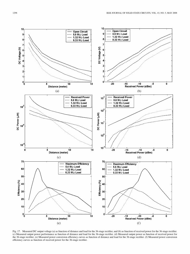
Fig. 17. Measured DC output voltage (a) as function of distance and load for the 36-stage rectifier, and (b) as function of received power for the 36-stage rectifier.(c) Measured output power performance as function of distance and load for the 36-stage rectifier. (d) Measured output power as function of received power forthe 36-stage rectifier. (e) Measured power conversion efficiency curves as function of distance and load for the 36-stage rectifier. (f) Measured power conversionefficiency curves as function of received power for the 36-stage rectifier.

LE et al.: EFFICIENT FAR-FIELD RADIO FREQUENCY ENERGY HARVESTING FOR PASSIVELY POWERED SENSOR NETWORKS 1299
slightly to increase the resonant frequency to 906 MHz. For thewireless measurement of the RF-DC power conversion circuit,the center frequency is set at 906 MHz for the 36-stage rectifierdesign.
Fig. 17(a) and (b) shows the measured output voltage of the36-stage rectifier as a function of distance and input power forvarious resistive loads. The 36-stage conversion circuit is ca-pable of outputting DC signal levels of 2 V at distances up to15 meters with a 36 dBm radiating source when it is not loadedas shown in Fig. 17(a). The measured output DC voltage de-creases exponentially as distance increases and also decreasesas the load resistance is decreased. With a 0.33 M load, theconversion circuit operates within 7 meters from the radiatingsource while providing 1 V DC. From observation, the oper-ating distance of the rectifier reduces quickly as the load cur-rent is increased while at closer distances, the dependence onload current is much less. Fig. 17(b) shows the output voltagecurves of the 36-stage design as function of received power cal-culated from the Friis equation for free-space propagation loss.The slope of the output voltage curves is relatively constant overthe full range since the output voltage is inversely proportionalto the log of the operating distance. The 36-stage design operateswell when the received power is higher than 22 dBm. Mea-surement of the far-field RF power harvesting system is donein a shielded lab, where the pathloss is enhanced by multipathand standing wave patterns. The same measurement is also per-formed in an open area with lower transmitted power and thedistance of the measurement is increased by up to 1.4 times.
Fig. 17(c) shows the measured output power as a functionof distance. The top curve represents the theoretical receivedpower in free-space as calculated by the Friis formula for free-space propagation loss given a 36 dBm radiating source. Witha 0.33 M resistive load, the current requirement at the load ishigher so more current is drawn from the output of the rectifierto drive the load hence the curve shows a steeper slope. Theslope of the roll off is directly proportional to the load currentat the output of the rectifier. With a 1.32 M load, 1 W at10 meters is possible and up to 12.3 meters with the 5.6 Mload. Fig. 17(d) shows the output power as function of receivedpower. From this plot, the point where the power curve startsto roll off from the straight (open circuit) line can be seen moreclearly. For the 36-stage rectifier design, the output power startsto roll off at about 8 dBm for the 0.33 M load, 13 dBm forthe 1.32 M load, and 18 dBm for the 5.6 M load.
The measured power conversion efficiency versus distancecurves are shown in Fig. 17(e) and (f). The power conversionefficiency curve for each individual load is shown as well asthe maximum efficiency that can be achieved at a particulardistance. For a perfectly matched resonator network, the poweravailable for rectification is half of the received power inthe antenna since only half of the power is dissipated in therectifier. The power conversion efficiency of the RF-DC powerconversion system is defined as the ratio between the DC outputpower and available power for rectification (half of the receivedpower) from the antenna. The maximum efficiency measured is60% with the 0.33 M load. The power conversion efficiency
Fig. 18. Measured energy extracted per hour as function of distance for the36-stage rectifier.
peaks at around 8 dBm received power due to the fact that theoutput voltage reaches a maximum point of approximately 9 V,due to the reverse breakdown voltage of the p-n junctions. Thispeak can be moved or optimized, for example, by changing thenumber of rectifier stages and transistor sizes. For lower loadcurrents, the power conversion efficiency is optimized at lowerreceived power or longer distances from the RF source. Onthe other hand, at higher load currents, the power conversionefficiency is optimized at higher received power or shorterdistances. The design of the 36-stage rectifier shows highestefficiency at 3 meters with a 0.33 M load, and the powerconversion efficiency curves rolls off as the inverse of distancefrom the RF source. The peak efficiency with the 5.6 M and1.32 M load is 29% at about 9 meters and 35% at about5 meters, respectively.
Fig. 18 shows the maximum energy that can be extractedfrom the RF signal in one hour at various distances from theradiating source. From the logarithmic plot of extracted energyagainst distance, the extracted energy curve is approximatelya straight line. The maximum extractable energy in an hour is0.8 J at 1 meter, 40 mJ at 5 meters, 7 mJ at 10 meters and about1 mJ at 15 meters from the source. With one hour charge time,the RF-DC power conversion circuit acquires and replenishesenough energy to operate a circuit that dissipates 1 mW for onesecond or 100 mW for 10 ms at distances up to 15 meters. Foran increase of every meter in distance, the amount of energythat can be extracted from the RF signal is reduced by a factorof 2.6. This establishes the trade off between power dissipationand operating distance of the integrated circuit powered by theRF-DC power conversion circuit.
Fig. 19(a) compares the voltage performance of the 36-stagepower conversion circuit with recently published work [28],[29]. The work in [29], [30] uses an active switched capacitorcircuit with a clock generator and an external power supply toactively bias the gate-source voltage of the diode-tied transistorin the rectifier circuit. The work in [28] uses a passive method

1300 IEEE JOURNAL OF SOLID-STATE CIRCUITS, VOL. 43, NO. 5, MAY 2008
Fig. 19. (a) Output DC voltage as function of the input power. (b) Output DC power as function of the sinusoidal input. (c) Power conversion efficiency as functionof the sinusoidal input.
to bias the gate-source voltage of the diode-tied transistor, how-ever, the passive circuit does require static power to maintainthe gate-source bias. This gate-source bias needs a large turn-onsinusoidal signal to start-up and takes a long time for the bias tocharge up when a signal level below threshold voltage is applied.Once the power source is turned off, the gate-source bias will bedischarged from the static current. The work in [29] requires thegeneration of a bias voltage which uses a reference currentin the nanoamp range, although the static power dissipated fromthe resistor is minimal, it causes a bias voltage much less thanthe desired threshold voltage. In other words, the voltage dropacross a diode-tied transistor under 2 nA bias is much differentthan one drawing 2 A of current. This voltage difference is typ-ically 100 mV for every decade of current difference. Also, thismethod would require extra circuitry to generate a voltage biasand a differential clock and it would also require a secondarybattery. The results obtained from [28] and [29] are measuredfrom an applied sinusoidal input and the distance performance is
calculated using the Friis equation for free-space. Distance per-formance in this work is the actual measured distance from theradiation source. Because [28] and [29] both have voltage regu-lation, only the voltage at the far distance is compared. The rec-tifier design in [29] is one stage, and in [28] is six stages, hencethe output voltage is much lower than the 36-stage design undera 5.6 M load, however, the output current with the 5.6 M loadis lower compared to [28] and [29]. With the 0.33 M load, thecurrent is increased but the output voltage is only comparable tothe other two designs.
Fig. 19(b) shows the output power curves for the same threedesigns. The output power of this work greatly exceeds other de-signs and, for received power below 20 dBm, it gives outputpower level 5 times the output power of the closest design.The comparison of the power conversion efficiency is shown inFig. 19(c). This design is 30% more efficient throughout the fullrange with a peak efficiency of 60%. Table II summarizes thiswork as compared to previously published work.

LE et al.: EFFICIENT FAR-FIELD RADIO FREQUENCY ENERGY HARVESTING FOR PASSIVELY POWERED SENSOR NETWORKS 1301
TABLE IIPERFORMANCE SUMMARY
VI. CONCLUSION
A passively powered RF-DC conversion circuit operating at906 MHz is presented. A novel rectifier circuit is designed anddemonstrated to work with signals as low as 50 mV and hasa maximum measured efficiency of 60%. This allows an in-crease in the operable distance between the circuit and the radi-ation source. The system operates with received power as lowas 22.6 dBm (5.5 W), corresponding to 42 meters distancein free-space with a 4 W radiation source. A measured distanceof 15 meters is achieved with 1 V DC and a 0.3 A load current.
REFERENCES
[1] S. Meninger, “A low power controller for a MEMS based energy con-verter,” Master’s thesis, Dept. Electr. Eng. Comput. Sci., Mass. Inst.Technol., Cambridge, MA, Jun. 1999.
[2] K. Finkenzeller, RFID Handbook: Fundamentals and Applicationsin Contactless Smart Cards and Identification, 2nd ed. Chicester,Sussex, U.K.: Wiley, 2003.
[3] S. Chatzandroulis, D. Tsoukalas, and P. A. Neukomm, “A miniaturepressure system with a capacitive sensor and a passive telemetry linkfor use in implantable applications,” J. Microelectromech. Syst., vol. 9,no. 1, pp. 18–23, Mar. 2000.
[4] D. Dudenbostel, K. L. Krieger, C. Candler, and R. Laur, “A new passiveCMOS telemetry chip to receive power and transmit data for a widerange of sensor applications,” in Proc. Int. Conf. Solid State SensorsActuators, Jun. 1997, vol. 2, pp. 16–19.
[5] K. J. Cho and H. H. Asada, “A recursive frequency tracking methodfor passive telemetry sensors,” in Proc. 2003 Amer. Control Conf., Jun.2003, vol. 6, pp. 4943–4948.
[6] F. Kocer, P. Walsh, and M. Flynn, “Wireless, remotely poweredtelemetry in 0.25 �m CMOS,” in 2004 IEEE Radio Frequency Inte-grated Circuits (RFIC) Systems Dig. Papers, Forth Worth, TX, Jun.2004, pp. 339–342.
[7] A.-L. Annala, I. Oy, and U. Friedrich, “Passive long Distance MultipleAccess UHF RFID System (RFID),” Palomar Project, European Com-mission, Public Report, Project No. IST1999-10339, Nov. 2002.
[8] Q. Huang and M. Oberle, “A 0.5-mW passive telemetry IC forbiomedical applications,” IEEE J. Solid-State Circuits, vol. 33, no. 7,pp. 937–946, Jul. 1998.
[9] T. Lehmann and Y. Moghe, “On-chip active power rectifiers forbiomedical applications,” in IEEE Int. Symp. Circuits Syst. (ISCAS),Kobe, Japan, May 2005, vol. 1, pp. 732–735.
[10] J. U. M. Araiza, “Wireless transmission of power for sensors in contextaware systems,” Master’s thesis, Dept. Electr. Eng. Comput. Sci., Mass.Inst. Technol., Cambridge, MA, Jun. 2002.
[11] T. Le, K. Mayaram, and T. S. Fiez, “Efficient far-field radio frequencypower conversion system for passively powered sensor networks,” inProc. IEEE Custom Integrated Circuits Conf. (CICC), Sep. 2006, pp.293–296.
[12] S. Mandal, “Far field RF power extraction circuits and systems,”Master’s thesis, Dept. Electr. Eng. Comput. Sci., Mass. Inst. Technol.,Cambridge, MA, Jun. 2004.
[13] S. Mandal and R. Sarpeshkar, “Low-power CMOS rectifier design forRFID applications,” IEEE Trans. Circuits Syst. I, vol. 54, no. 6, pp.1177–1188, Jun. 2007.
[14] M. Hata, “Empirical formula for propagation loss in land-mobile radioservice,” IEEE Trans. Veh. Technol., vol. VT-29, no. 3, pp. 317–325,Aug. 1980.
[15] U. Karthaus and M. Fischer, “Fully integrated passive UHF RFIDtransponder IC with 16.7-�W minimum RF input power,” IEEE J.Solid-State Circuits, vol. 38, no. 10, pp. 1602–1608, Oct. 2003.
[16] J. F. Dickson, “On-chip high-voltage generation in MNOS integratedcircuits using an improved voltage multiplier technique,” IEEE J. Solid-State Circuits, vol. SSC-11, no. 3, pp. 374–378, Jun. 1976.
[17] J.-T. Wu and K.-L. Chang, “MOS charge pumps for low-voltage oper-ation,” IEEE J. Solid-State Circuits, vol. 33, no. 4, pp. 592–597, Apr.1998.
[18] A. S. Sedra and K. C. Smith, Microelectronic Circuits, 4th ed. Ox-ford, U.K.: Oxford Univ. Press, 1998.
[19] H. T. Friis, “A note on a simple transmission formula,” Proc. IRE, vol.34, no. 5, pp. 254–256, May 1946.
[20] FCC Codes of Regulation, pt. 15 [Online]. Available: http://www.ac-cess.gpo.gov/nara/cfr/waisidx_03/47cfr15_03.htm
[21] T. H. Lee, The Design of CMOS Radio Frequency Integrated Circuits,2nd ed. Cambridge, U.K.: Cambridge Univ. Press, 2004.
[22] I. J. Bahl, “High-Q and low-loss matching network elements for RFand microwave circuits,” in IEEE MTT-S Int. Microw. Symp. Dig., Sep.2000, vol. 1, no. 3, pp. 64–73.
[23] P. Cole, M. L. Ng, and K. S. Leong, Some notes on antenna matchingand measurement for small RFID tags [Online]. Available: http://au-toidlab.adelaide.edu.au.
[24] B. Razavi, Design of Analog CMOS Integrated Circuits. New York:McGraw-Hill, 2001.
[25] T. Le, J. Han, A. von Jouanne, K. Mayaram, and T. S. Fiez, “Piezo-electric power generation interface circuits,” in Proc. IEEE Custom In-tegrated Circuit Conf. (CICC), Sep. 2003, pp. 489–492.
[26] J. Killen, “Utilizing standard CMOS process floating gate devices foranalog design,” Master’s Thesis, Dept. Electr. Comput. Eng., Missis-sippi State Univ., Starkville, Aug. 2001.
[27] F. Kocer, P. Walsh, and M. Flynn, “An RF powered, wireless tempera-ture sensor in quarter micron CMOS,” in Proc. IEEE Int. Symp. CircuitsSyst. (ISCAS), May 2004, vol. 4, pp. 23–26.
[28] H. Nakamoto et al., “A passive UHF RFID tag LSI with 36.6% ef-ficiency CMOS-only rectifier and current-mode demodulator in 0.35um FERAM technology,” in 2006 IEEE Int. Solid-State Circuits Conf.Dig. Tech. Papers, Feb. 2006, pp. 310–311.
[29] T. Umeda et al., “A 950 MHz rectifier circuit for sensor networks with10-m distance,” in 2005 IEEE Int. Solid-State Circuits Conf., San Fran-cisco, CA, Feb. 2005, vol. 1, pp. 256–597.
[30] T. Umeda, H. Yoshida, S. Sekine, Y. Fujita, T. Suzuki, and S. Otaka, “A950-MHz rectifier circuit for sensor network tags with 10-m distance,”IEEE J. Solid-State Circuits, vol. 41, no. 1, pp. 35–41, Jan. 2006.

1302 IEEE JOURNAL OF SOLID-STATE CIRCUITS, VOL. 43, NO. 5, MAY 2008
[31] J. Yi, W.-H. Ki, and C.-Y. Tsui, “Analysis and design strategy of UHFmicro-power CMOS rectifiers for microsensor and RFID applications,”IEEE Trans. Circuits Syst. I, vol. 54, no. 1, pp. 153–166, Jan. 2007.
[32] B. Wang, C.-H. Wang, Y. Ma, C. Diorio, and T. Humes, “Study ofstress-induced leakage current and charge loss of nonvolatile memorycell with 70 tunnel oxide using floating-gate integrator technique,”in 2004 IEEE Int. Integrated Rel. Workshop Final Rep., South LakeTahoe, CA, Oct. 2004, pp. 28–31.
[33] J.-P. Curty, N. Joehl, C. Dehollain, and M. Declercq, “Remotely pow-ered addressable UHF RFID integrated system,” IEEE J. Solid-StateCircuits, vol. 40, no. 11, pp. 2193–2202, Nov. 2005.
[34] R. Barnett, S. Lazar, and J. Liu, “Design of multistage rectifiers withlow-cost impedance matching for passive RFID tags,” in Proc. IEEERFIC Symp. Dig., Jun. 2006, pp. 291–294.
[35] G. De Vita and G. Iannaccone, “Design criteria for the RF section ofUHF and microwave passive RFID transponders,” IEEE Trans. Mi-crow. Theory Tech., vol. 53, no. 9, pp. 2978–2990, Sep. 2005.
Triet Le received the B.S. and Ph.D. degrees in elec-trical engineering from Oregon State University, Cor-vallis, in 2001 and 2008, respectively.
His research interest is in analog and mixed-signalIC design for low-power applications.
Mr. Le was the recipient of the Outstanding Stu-dent Designer Award presented by Analog DevicesInc. in 2003.
Kartikeya Mayaram (S’82–M’88–SM’99–F’05)received the B.E. (Hons.) degree in electrical engi-neering from the Birla Institute of Technology andScience, Pilani, India, in 1981, the M.S. degree inelectrical engineering from the State University ofNew York, Stony Brook, in 1982, and the Ph.D.degree in electrical engineering from the Universityof California, Berkeley, in 1988.
From 1988 to 1992, he was a Member of Tech-nical Staff in the Semiconductor Process and DesignCenter of Texas Instruments, Dallas, TX. From 1992
to 1996, he was a Member of Technical Staff at Bell Labs, Allentown, PA. Hewas an Associate Professor in the School of Electrical Engineering and Com-puter Science at Washington State University, Pullman, from 1996 to 1999 andin the Electrical and Computer Engineering Department at Oregon State Uni-versity, Corvallis, from 2000 to 2003. Now he is a Professor in the School ofElectrical Engineering and Computer Science at Oregon State University. Hisresearch interests are in the areas of circuit simulation, device simulation andmodeling, simulation and modeling of substrate coupling in mixed-signal ICs,integrated simulation environments for microsystems, and analog/RF design.
Dr. Mayaram received the National Science Foundation (NSF) CAREERAward in 1997. He has served on the technical program committees of sev-eral conferences and was on the editorial board of IEEE TRANSACTIONS ON
COMPUTER-AIDED DESIGN OF INTEGRATED CIRCUITS AND SYSTEMS as an As-sociate Editor from 1995–2001 and as the Editor-in-Chief from 2002–2005.
Terri S. Fiez (S’82–M’85–SM’95–F’05) receivedthe B.S. and M.S. degrees in electrical engineeringfrom the University of Idaho, Moscow, in 1984and 1985, respectively, and the Ph.D. degree inelectrical and computer engineering from OregonState University, Corvallis, in 1990.
In 1990, she joined Washington State Universityas an Assistant Professor where she became anAssociate Professor in 1996. In the fall of 1999, shejoined the Department of Electrical and ComputerEngineering at Oregon State University as Professor
and Department Head. She became Director of the School of Electrical Engi-neering and Computer Science in 2003. Her research interests are in the designof high-performance analog signal processing building blocks, simulation andmodeling of substrate coupling effects in mixed-signal ICs, and innovativeengineering education approaches.
Prof. Fiez has been involved in a variety of IEEE activities including servingon the committees for the IEEE International Solid-State Circuits Conference,IEEE Custom Integrated Circuits Conference, and ISCAS, and as electedAdCom for the Solid-State Circuits Society. She previously received the NSFYoung Investigator Award, the Solid-State Circuit Predoctoral Fellowship, andthe 2006 IEEE Education Activities Board Innovative Education Award.