IEEE Journal of Emerging and Selected Topics in Power ... such as in a series resonant converter...
9
Variable Frequency Multiplier Technique for High Efficiency Conversion Over a Wide Operating Range Wardah Inam, Student Member, IEEE, Khurram K. Afridi, Member, IEEE, and David J. Perreault, Fellow, IEEE Abstract—This paper presents a Variable Frequency Multiplier (VFX) technique that enables design of converters for wide input and/or output voltage ranges while preserving high efficiency. The technique is applied to an LLC converter to demonstrate its effec- tiveness for converters having wide input voltage variation such as universal input power supplies. This technique compresses the effective operating range required of a resonant converter by switching the inverter and/or rectifier operation between processing energy at a fundamental frequency and one or more harmonic frequencies. The implemented converter operates over an input voltage range of 85 V to 340 V but the resonant tank and conversion ratio has only been designed for half this range; a VFX mode of the inverter is used to enhance this to the full range. Experimental results from a 50 W converter show an efficiency of 94.9% to 96.6% across the entire input voltage range, demonstrating the advantage of using this technique in such applications. Index Terms- dc/dc converter, power supplies resonant converter, high efficiency power converter, variable frequency multiplier I. I NTRODUCTION A trend in power electronics has been to strive for high power density and high efficiency across a wide operating range [1]. High power density can be achieved by switching power converters at a high frequency. At these high frequen- cies, resonant converters use soft switching (i.e. Zero Voltage Switching (ZVS) and/or Zero Current Switching (ZCS)) to reduce switching losses to achieve high efficiency [2], [3]. Although soft-switched resonant converters can achieve high efficiency at a nominal operating point, the efficiency tends to degrade considerably with variations in input voltage, output voltage and power level [4]. Resonant converters commonly use frequency control [2], [3] and/or phase shift control [5], [6] to compensate for variations in input voltage and power levels. If switching frequency is increased to reduce output power or gain of the converter, such as in a series resonant converter operated above resonance to maintain ZVS, switching losses increase. Also, with operation over a wide frequency range as often required in resonant converters, the magnetics cannot be optimally de- signed. Furthermore, circulating currents may increase propor- tionally as load is decreased resulting in higher losses at light loads. With phase shift control, operation over a wide range is likewise challenging. In many resonant converters, when two legs of the inverter are phase shifted with respect to each other, they have asymmetrical current levels at the switching transitions. The leading inverter leg can lose ZCS and the lagging leg can lose ZVS. Other control techniques such as asymmetrical current mode control [7] and asymmetrical duty cycle PWM control [8] also have limitations such as loss of ZVS. In this paper, a Variable Frequency Multiplier (VFX) tech- nique is introduced and its effectiveness is demonstrated for a universal input power supply. In the VFX technique, additional ”frequency multiplier” modes of operation of the inverter and/or rectifier are used to provide additional sets of operating characteristics for the converter to achieve and maintain high performance across a wide operating range. Frequency multiplier circuits are often used in extreme high- frequency RF applications (e.g., where transistor f T is a concern), and are sometimes used in switched-mode inverters and power amplifiers (e.g., [9], [10]). While it has been proposed to employ frequency multipliers in dc-dc converters (e.g., [11]), this is not usually done, as the output power of a frequency multiplier inverter is inherently low relative to the needed device ratings. However, here we propose using frequency multiplication as an additional operating mode of the inverter and/or rectifier, for wide-range voltage and/or power conditions. In this context, frequency multiplication can be used to extend the efficient operating range of a converter and improve its performance across power and voltage. It is noted that the concept of using frequency multiplication with multiple gain settings was employed in the inverter of a high-power dc-dc converter in reference [12]. However, this approach is suited to extremely high-power/high-voltage designs where multilevel inverter structures are feasible and enable flexibility in selecting operating methodologies. In comparison we describe an approach which does not require the high flexibility of multilevel inverters to provide wide- range operation. Moreover, we exploit the proposed concept in the context of a universal-input power supply, in which two separate gain settings can be effectively utilized in different op- erating environments (different regions of the world) without frequent mode shifting. As will be seen, this application of the concept is valuable because mode shifting imposes rebalancing of dc capacitor voltage levels which can be difficult to apply on a frequent basis. While the proposed VFX technique can be applied to the inverter and/or rectifier and for wide input and/or output voltage ranges, here we demonstrate it for wide input voltage range using VFX operation of the inverter and describe how this can be applied to the rectifier. Universal input power supplies need to operate over a wide input voltage range and IEEE Journal of Emerging and Selected Topics in Power Electronics (to appear)
Transcript of IEEE Journal of Emerging and Selected Topics in Power ... such as in a series resonant converter...

Variable Frequency Multiplier Technique for HighEfficiency Conversion Over a Wide Operating
RangeWardah Inam, Student Member, IEEE, Khurram K. Afridi, Member, IEEE, and David J. Perreault, Fellow, IEEE
Abstract—This paper presents a Variable Frequency Multiplier
(VFX) technique that enables design of converters for wide input
and/or output voltage ranges while preserving high efficiency. The
technique is applied to an LLC converter to demonstrate its effec-
tiveness for converters having wide input voltage variation such
as universal input power supplies. This technique compresses
the effective operating range required of a resonant converter
by switching the inverter and/or rectifier operation between
processing energy at a fundamental frequency and one or more
harmonic frequencies. The implemented converter operates over
an input voltage range of 85 V to 340 V but the resonant tank
and conversion ratio has only been designed for half this range;
a VFX mode of the inverter is used to enhance this to the full
range. Experimental results from a 50 W converter show an
efficiency of 94.9% to 96.6% across the entire input voltage
range, demonstrating the advantage of using this technique in
such applications.
Index Terms- dc/dc converter, power supplies resonant converter,
high efficiency power converter, variable frequency multiplier
I. INTRODUCTION
A trend in power electronics has been to strive for highpower density and high efficiency across a wide operatingrange [1]. High power density can be achieved by switchingpower converters at a high frequency. At these high frequen-cies, resonant converters use soft switching (i.e. Zero VoltageSwitching (ZVS) and/or Zero Current Switching (ZCS)) toreduce switching losses to achieve high efficiency [2], [3].Although soft-switched resonant converters can achieve highefficiency at a nominal operating point, the efficiency tends todegrade considerably with variations in input voltage, outputvoltage and power level [4].
Resonant converters commonly use frequency control [2],[3] and/or phase shift control [5], [6] to compensate forvariations in input voltage and power levels. If switchingfrequency is increased to reduce output power or gain of theconverter, such as in a series resonant converter operated aboveresonance to maintain ZVS, switching losses increase. Also,with operation over a wide frequency range as often requiredin resonant converters, the magnetics cannot be optimally de-signed. Furthermore, circulating currents may increase propor-tionally as load is decreased resulting in higher losses at lightloads. With phase shift control, operation over a wide rangeis likewise challenging. In many resonant converters, whentwo legs of the inverter are phase shifted with respect to eachother, they have asymmetrical current levels at the switchingtransitions. The leading inverter leg can lose ZCS and thelagging leg can lose ZVS. Other control techniques such as
asymmetrical current mode control [7] and asymmetrical dutycycle PWM control [8] also have limitations such as loss ofZVS.
In this paper, a Variable Frequency Multiplier (VFX) tech-nique is introduced and its effectiveness is demonstratedfor a universal input power supply. In the VFX technique,additional ”frequency multiplier” modes of operation of theinverter and/or rectifier are used to provide additional setsof operating characteristics for the converter to achieve andmaintain high performance across a wide operating range.Frequency multiplier circuits are often used in extreme high-frequency RF applications (e.g., where transistor f
T
is aconcern), and are sometimes used in switched-mode invertersand power amplifiers (e.g., [9], [10]). While it has beenproposed to employ frequency multipliers in dc-dc converters(e.g., [11]), this is not usually done, as the output power ofa frequency multiplier inverter is inherently low relative tothe needed device ratings. However, here we propose usingfrequency multiplication as an additional operating mode ofthe inverter and/or rectifier, for wide-range voltage and/orpower conditions. In this context, frequency multiplication canbe used to extend the efficient operating range of a converterand improve its performance across power and voltage. Itis noted that the concept of using frequency multiplicationwith multiple gain settings was employed in the inverter ofa high-power dc-dc converter in reference [12]. However,this approach is suited to extremely high-power/high-voltagedesigns where multilevel inverter structures are feasible andenable flexibility in selecting operating methodologies. Incomparison we describe an approach which does not requirethe high flexibility of multilevel inverters to provide wide-range operation. Moreover, we exploit the proposed conceptin the context of a universal-input power supply, in which twoseparate gain settings can be effectively utilized in different op-erating environments (different regions of the world) withoutfrequent mode shifting. As will be seen, this application of theconcept is valuable because mode shifting imposes rebalancingof dc capacitor voltage levels which can be difficult to applyon a frequent basis.
While the proposed VFX technique can be applied to theinverter and/or rectifier and for wide input and/or outputvoltage ranges, here we demonstrate it for wide input voltagerange using VFX operation of the inverter and describe howthis can be applied to the rectifier. Universal input powersupplies need to operate over a wide input voltage range and
IEEE Journal of Emerging and Selected Topics in Power Electronics (to appear)

vinv1
+
_Vin
S1
S2
S3
S4
Cin
Cin v
inv2
vinv
+
_+
_
+
_
Vbus
Figure 1: Stacked bridge inverter with input voltage Vin
andoutput voltage v
inv
.
it is a challenge to design resonant power converters for suchwide range of operation. In this paper, we demonstrate theVFX technique employed in the inverter of an LLC resonantconverter designed to operate across a 4:1 input voltage rangeof 85 V to 340 V.
This paper is organized as follows. In section II, the VariableFrequency Multiplier technique is introduced and discussedfor an inverter and rectifier. Section III presents the designand analysis of a dc/dc LLC converter operating in two VFXmodes for a universal input power supply. Experimental resultsof the prototype are presented in section IV, and section Vconcludes the paper.
II. VARIABLE FREQUENCY MULTIPLIER
The Variable Frequency Multiplier (VFX) technique can beapplied to the inverter stage and/or rectifier stage of a converterto achieve wide input voltage and/or output voltage rangeoperation or to extend the efficient operating power range. Inthis technique, the duty ratio and the switching frequency ofan inverter and/or rectifier is changed as input and/or outputvoltages change such that it processes power between dc anda specific harmonic of its switching frequency (rather thanjust its fundamental) to create different modes of operation.By operating between dc and a higher harmonic, the dc-ac(or ac-dc) voltage gain of the inverter or rectifier changes,and one gains an added operating mode with different transfercharacteristics. In case of frequency control this allows theconverter to be operated over a narrower (intermediate ac)frequency range for a wide voltage conversion range and/orpower range. Depending on the circuit architecture, more thantwo modes can be created.
This paper describes the use of the VFX technique appliedto the inverter stage and/or rectifier stage of resonant orother ac-link converters. To demonstrate the utility of thistechnique, we have built an LLC converter with a two-modeVFX technique applied to the inverter stage to efficientlyextend the input voltage range of the converter.
A. Technique Applied to an Inverter
To understand the VFX technique applied to an inverterconsider the stacked bridge inverter as shown in Fig. 1 withan output voltage v
inv
(vinv
= vinv1 + V
bus
� vinv2).
This inverter under VFX control operates in two modes:Fundamental VFX mode (mode 1) and second harmonic VFX
+
_Vin
S1
S2
S1
S3
S4
Cin
Cin
vinv
+
_
(a) State a
+
_Vin
S1
S2
S1
S3
S4
Cin
Cin
vinv
+
_
(b) State b
Figure 2: Stacked bridge inverter with input voltage Vin
andoutput voltage v
inv
in mode 1.
vinv1
vinv2
Vin/2
Vin/2
vinv
Vin
a
Vbus
b
0.5T T
t
Figure 3: Output voltages of the two inverters vinv1 and v
inv2
and the resultant inverter voltage vinv
in Mode 1.
mode (mode 2). This change in mode is synthesized bychanging the switching pattern of the inverter switches andit results in an output voltage (v
inv
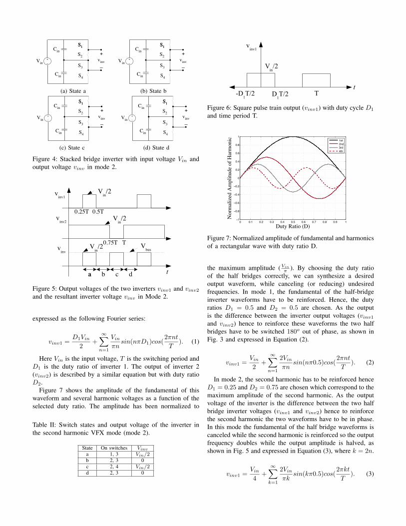
) which is of differentmagnitude hence it changes the voltage gain of the inverter.In mode 1, there are two switching states in one switchingperiod as summarized in Table I. In state a switches 1 and4 are on and in state b switches 2 and 3 are on as shown inFig. 2. Mode 1 results in twice the amplitude of the individualinverter outputs as shown in Fig. 3.
In mode 2, there are four switching states in one switchingperiod as summarized in Table II. The VFX mode results inhalf the gain and double the frequency of the output waveformfor a single switching cycle as shown in Fig. 5. Thus for thetransformation stage to see the same frequency as in mode 1,in this mode the converter is operated at half the switchingfrequency of mode 1 (with each switching device operating athalf the rate of the output ac waveform).
To create these switching patterns and to extend this to othertopologies, frequency analysis is useful. Considering Fourieranalysis, the square pulse output of inverter 1 (Fig. 6) can be
Table I: Switch states and the output voltage of the inverter infundamental VFX mode (Mode 1).
State On switches vinv
a 1, 4 Vin
b 2, 3 0
+
_Vin
S1
S2
S1
S3
S4
Cin
Cin
vinv
+
_
(a) State a
+
_Vin
S1
S2
S1
S3
S4
Cin
Cin
vinv
+
_
(b) State b
+
_Vin
S1
S2
S1
S3
S4
Cin
Cin
vinv
+
_
(c) State c
+
_Vin
S1
S2
S1
S3
S4
Cin
Cin
vinv
+
_
(d) State d
Figure 4: Stacked bridge inverter with input voltage Vin
andoutput voltage v
inv
in mode 2.
vinv1
vinv2
Vin/2
Vin/2
a b c d
Vbus
Vin/2v
inv
t
0.25T
a
0.5T
0.75T T
Figure 5: Output voltages of the two inverters vinv1 and v
inv2
and the resultant inverter voltage vinv
in Mode 2.
expressed as the following Fourier series:
vinv1 =
D1Vin
2+
1X
n=1
Vin
⇡nsin(n⇡D1)cos(
2⇡nt
T). (1)
Here Vin
is the input voltage, T is the switching period andD1 is the duty ratio of inverter 1. The output of inverter 2(v
inv2) is described by a similar equation but with duty ratioD2.
Figure 7 shows the amplitude of the fundamental of thiswaveform and several harmonic voltages as a function of theselected duty ratio. The amplitude has been normalized to
Table II: Switch states and output voltage of the inverter inthe second harmonic VFX mode (mode 2).
State On switches Vinv
a 1, 3 Vin
/2b 2, 3 0c 2, 4 V
in
/2d 2, 3 0
D1T/2
Vin/2
t
vinv1
T-D1T/2
Figure 6: Square pulse train output (vinv1) with duty cycle D1
and time period T.
0 0.1 0.2 0.3 0.4 0.5 0.6 0.7 0.8 0.9 1−1
−0.8
−0.6
−0.4
−0.2
0
0.2
0.4
0.6
0.8
1
Duty Ratio (D)N
orm
aliz
ed A
mpl
itude
of H
arm
onic
1st2nd3rd4th
Figure 7: Normalized amplitude of fundamental and harmonicsof a rectangular wave with duty ratio D.
the maximum amplitude (Vin
⇡
). By choosing the duty ratioof the half bridges correctly, we can synthesize a desiredoutput waveform, while canceling (or reducing) undesiredfrequencies. In mode 1, the fundamental of the half-bridgeinverter waveforms have to be reinforced. Hence, the dutyratios D1 = 0.5 and D2 = 0.5 are chosen. As the outputis the difference between the inverter output voltages (v
inv1
and vinv2) hence to reinforce these waveforms the two half
bridges have to be switched 180o out of phase, as shown inFig. 3 and expressed in Equation (2).
vinv1 =
Vin
2+
1X
n=1
2Vin
⇡nsin(n⇡0.5)cos(
2⇡nt
T). (2)
In mode 2, the second harmonic has to be reinforced henceD1 = 0.25 and D2 = 0.75 are chosen which correspond to themaximum amplitude of the second harmonic. As the outputvoltage of the inverter is the difference between the two halfbridge inverter voltages (v
inv1 and vinv2) hence to reinforce
the second harmonic the two waveforms have to be in phase.In this mode the fundamental of the half bridge waveforms iscanceled while the second harmonic is reinforced so the outputfrequency doubles while the output amplitude is halved, asshown in Fig. 5 and expressed in Equation (3), where k = 2n.
vinv1 =
Vin
4+
1X
k=1
2Vin
⇡ksin(k⇡0.5)cos(
2⇡kt
T). (3)

Q3
Q4
Q1
Q2
vR1
vR2RL
Co
IRo +
VRo
-vRi=vR1-vR2
Figure 8: Full bridge synchronous rectifier with a resistiveoutput load.
For the same output frequency the two inverters switchat half the frequency. Note that in each case (for the two-mode VFX inverter) the ac output waveform is a square wave.This technique can thus be used in any number of ac linktopologies, including all kinds of resonant converters and dual-active bridge converters.
B. Technique Applied to a Synchronous Rectifier
A rectifier receives an ac current (or voltage) at its input andpresents an ac voltage (or current) at its input, which resultsin dc power being absorbed and delivered to the output as dcvoltage and current. The amount of power absorbed dependson the amplitude of the voltage (or current) presented at theinput of the rectifier. Hence, the VFX technique can likewisebe applied to the rectifier to make the ac voltage at its inputbe either at the fundamental of the rectifier devices switchingfrequency or at a harmonic of the devices switching frequencyin order to convert the ac input power to dc.
For example, consider a full bridge synchronous rectifieras shown in Fig. 8. Similar to the inverter presented in theprevious section, we can create two modes of operation bychanging the switching pattern of Q1, Q2, Q3 and Q4, whichdetermines the rectifier input voltage. In mode 1, the inputvoltage of leg 1 of the rectifier (v
R1) is equal to the rectifieroutput voltage (V
Ro
) for half the switching cycle (Q1 and Q4
switched on), while the input voltage of leg 2 of the rectifier(v
R2) is zero. In the second half of the switching cycle (Q2
and Q3 switched on) vR2 is equal to V
Ro
and vR1 is zero,
as shown in Fig. 9. The resulting voltage at the input of therectifier v
Ri
is the difference of the input voltages of the tworectifier legs (v
Ri
= vR1 � v
R2) and is either +VRo
or �VRo
with 50% duty ratio. The voltage waveform at the input of therectifier (shown in Fig. 9), can be used to determine the gainof the rectifier in mode 1.
MR,mode1 =
VRo
vRi,pk�pk
=VRo
2VRo
= 0.5. (4)
In mode 2, vR1 is equal to V
Ro
for 75% duty cycle and vR2
is phase shifted by 90 degrees and equal to VRo
for 25 % duty
vRi
+VRov
R1
-VRo
vR2
0.5T T
1.5T
+VRo
t+VRo
Figure 9: Voltage waveforms at the rectifier input during mode1.
+VRo
vRi
+VRo
vR1
+VRo
vR2
0.75T
0.25T 0.5T
T
T
T0.5T0.25T
t
Figure 10: Voltage waveforms at the rectifier input duringmode 2.
cycle. The resulting rectifier input voltage vRi
has twice thefrequency of the rectifier switches and is either V
Ro
or 0. Inorder to have the same input (ac) voltage frequency as mode1, the rectifier switches are switched at half the frequency ofmode 1 (with all devices operating at the same frequency).The resulting voltage waveforms are shown in Fig. 10 and asseen from the figure the gain of the rectifier doubles in mode2.
MR,mode2 =
VRo
vRi,pk�pk
=VRo
VRo
= 1. (5)
This gives us the opportunity to operate the converter withdouble the output voltage (if the input voltage remains thesame) effectively increasing the output voltage range of theconverter.
With the rectifier driven by a nearly sinusoidal currentwaveform (due to a resonant tank in a resonant converter),we can control the amount of power transferred by controllingthe phase difference between the current and the input voltageof the rectifier. Consider a simplified case when the inputvoltage and current are in phase: using Fundamental HarmonicApproximation (FHA) we can represent the effective input ofthe rectifier as an equivalent resistor (R
eqv
= k0RL
) where

RL
is the output load resistor, and ko
is a constant whichdepends on the ratio between the fundamental harmonic ofthe voltage and the current.
In mode 1, the fundamental frequency components of thevoltage waveform and the current waveform for the rectifierof Fig. 9 are given by:
vRi�ac,mode1 =
4
⇡VRo
sin(!t). (6)
iRi�ac,mode1 =
⇡
2IRo
sin(!t). (7)
Where VRo
is the dc rectifier output voltage, IRo
is the dcrectifier output current. The ratio of the ac voltage and current,representing the equivalent resistance, is given as:
Reqv,mode1 =
vRi�ac,mode1
iRi�ac,mode1
=8
⇡2R
L
. (8)
Where RL
is the dc load resistor at the output of the rectifier,equal to V
Ro
/IRo
(for continuous steady-state operation). Us-ing two-mode VFX technique, we alter the rectifier character-istics (while still operating with a “resistive” characteristic) bychanging the switching pattern of the switches. The magnitudeof the fundamental frequency component of the ac rectifierinput voltage v
Ri�ac
decreases by half:
vRi�ac,mode2 =
2
⇡VRo
sin(!t). (9)
For the same output power, IRo
increases by half, so theinput current is given by:
iRi�ac,mode2 = ⇡I
Ro
sin(!t). (10)
Hence, the equivalent resistance is equal to:
Reqv,mode1 =
2
⇡2R
L
. (11)
The second operating mode in VFX gives us the opportunityto adjust the voltage and current profile of the rectifier (e.g.,keeping an equivalent ac input resistance at a different dcoutput voltage, or changing the effective ac output resistancefor a given dc resistive loading on the rectifier).
The two-mode VFX technique presented can be easilyextended to higher modes, given an appropriate rectifierstructure. It can likewise be applied to many other rectifiertopologies, such as stacked rectifiers, voltage-fed rectifiers,current-doubler rectifier, etc.
III. DESIGN OF AN LLC CONVERTER OPERATING WITHVFX TECHNIQUE
We demonstrate the proposed technique in a dc-dc converterdesigned for a two-stage universal laptop power supply. The acvoltage varies in different countries but the nominal voltageis either 110-120 Vrms at 60 Hz, or 220-240 Vrms at 50Hz. Therefore, 120 Vrms and 240 Vrms have been selectedas the upper limits for the two modes of converter operation,corresponding to peak dc voltages of 170 V and 340 V appliedto the dc-dc converter. The variable frequency multiplier
Cr
Lr
Lm
n:1
D1
D2
+
Vout
_
S1
S2
S1
S3
S4
Cin
Cin
+
_Vin
Ir
Im
+Vcr
-
Vin
Vin
2
2
+
_
+
_
Vbus
Figure 11: Schematic of the LLC converter with a stackedbridge inverter incorporating the VFX technique.
technique is very useful for this application because there aretwo distinct peak input voltages.
An LLC converter has been selected for the dc/dc stage. Ituses frequency control to regulate the output voltage and hasmany advantages. The main advantages are that it has the capa-bility to regulate the output voltage over a wide range of inputvoltage and power with only a small variation in the switchingfrequency [13]. Also, it achieves zero voltage switching (ZVS)over the entire range of operation thus reducing the switchinglosses. Moreover, the leakage and magnetizing inductance ofthe transformer can be incorporated into the design.
Figure 11 shows the schematic of the LLC converter with aninverter appropriate for voltage step-down and VFX operation.As it has a high input voltage, stacked half bridges are used.This reduces the voltage stress of the transistors by half,which increases their performance with available devices. Thetransformation stage consists of a series inductor (L
r
) and acapacitor (C
r
) and a parallel inductor (Lm
). The capacitor notonly provides resonant filtering but also provides dc blockingfor flux balancing.
The transformer parasitics, leakage and magnetizing induc-tance, can be used instead of separate inductors [14]. A center-tapped transformer is used to reduce the number of seriesdiodes in the rectification path. This increases the loss of thetransformer and the voltage stress of the diodes. However, thistrade off is still beneficial because of the low output voltage.Synchronous rectification can be used to further reduce lossesin the rectification stage [15], [16], [17]. The converter isdesigned using the method outlined in [18]. FundamentalHarmonic Approximation (FHA) is used to analyze and designthe converter. Time-based [19] and approximate methods [20],[21] can be used for more accurate gain analysis.
The converter is designed for a maximum input voltage of170 V in the fundamental mode and an output voltage of 20 V.To ensure that the power supply (of which the dc/dc converteris the second stage) has a sufficiently high power factor (i.e.,greater than 0.95), the minimum input voltage for the dc-dcstage is 85 V. For input voltages above 170 V, the secondharmonic VFX mode is used to decrease the voltage that thetransformation stage sees by half.
Using Fundamental Harmonic Approximation, all the volt-ages and currents are represented by their fundamental com-ponents and the secondary-side variables are reflected to theprimary side to obtain the approximated circuit shown in Fig.
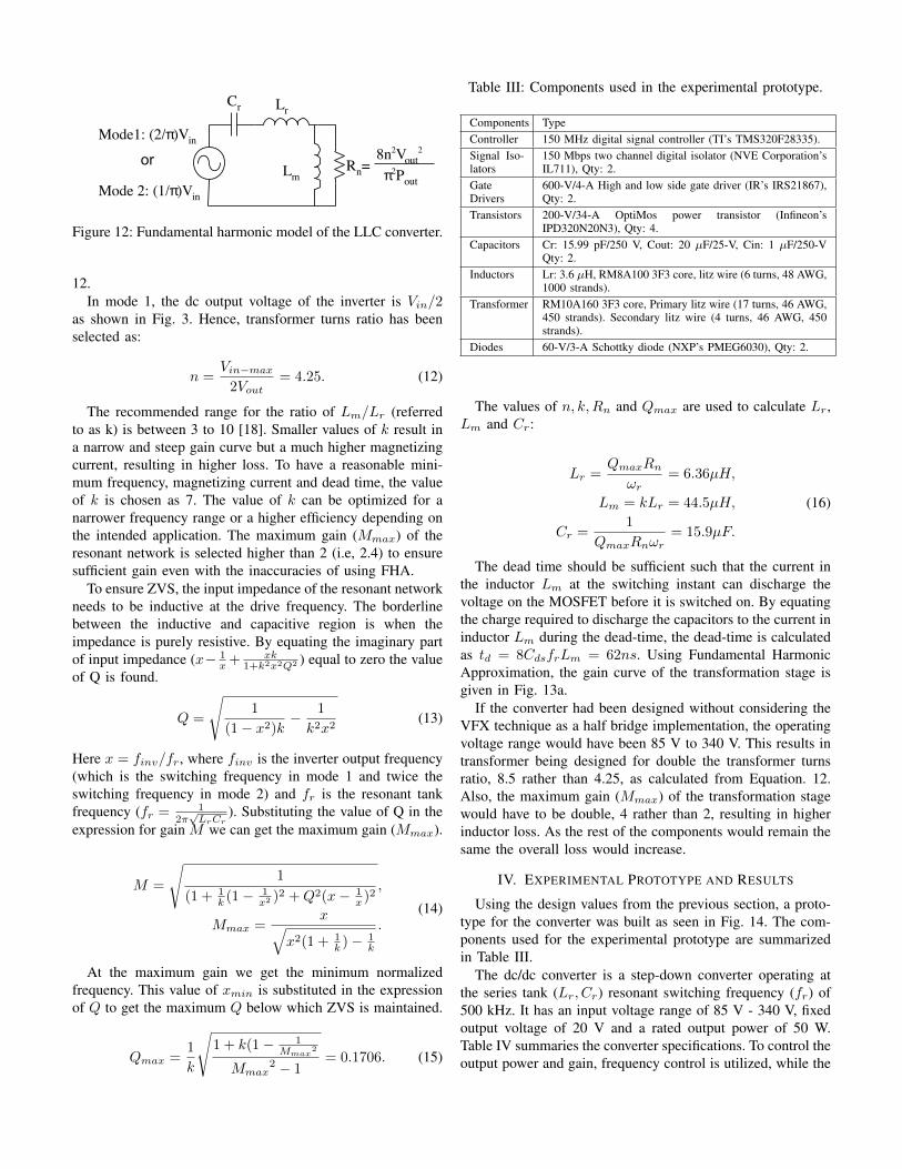
Cr Lr
Lmor
8n2Vout2
π2PoutRn=
Mode 2: (1/ )πVin
Mode1: (2/ )πVin
Figure 12: Fundamental harmonic model of the LLC converter.
12.In mode 1, the dc output voltage of the inverter is V
in
/2as shown in Fig. 3. Hence, transformer turns ratio has beenselected as:
n =Vin�max
2Vout
= 4.25. (12)
The recommended range for the ratio of Lm
/Lr
(referredto as k) is between 3 to 10 [18]. Smaller values of k result ina narrow and steep gain curve but a much higher magnetizingcurrent, resulting in higher loss. To have a reasonable mini-mum frequency, magnetizing current and dead time, the valueof k is chosen as 7. The value of k can be optimized for anarrower frequency range or a higher efficiency depending onthe intended application. The maximum gain (M
max
) of theresonant network is selected higher than 2 (i.e, 2.4) to ensuresufficient gain even with the inaccuracies of using FHA.
To ensure ZVS, the input impedance of the resonant networkneeds to be inductive at the drive frequency. The borderlinebetween the inductive and capacitive region is when theimpedance is purely resistive. By equating the imaginary partof input impedance (x� 1
x
+ xk
1+k
2x
2Q
2 ) equal to zero the valueof Q is found.
Q =
s1
(1� x2)k� 1
k2x2(13)
Here x = finv
/fr
, where finv
is the inverter output frequency(which is the switching frequency in mode 1 and twice theswitching frequency in mode 2) and f
r
is the resonant tankfrequency (f
r
= 12⇡
pL
r
C
r
). Substituting the value of Q in theexpression for gain M we can get the maximum gain (M
max
).
M =
s1
(1 + 1k
(1� 1x
2 )2 +Q2(x� 1x
)2,
Mmax
=xq
x2(1 + 1k
)� 1k
.(14)
At the maximum gain we get the minimum normalizedfrequency. This value of x
min
is substituted in the expressionof Q to get the maximum Q below which ZVS is maintained.
Qmax
=1
k
s1 + k(1� 1
M
max
2
Mmax
2 � 1= 0.1706. (15)
Table III: Components used in the experimental prototype.
Components TypeController 150 MHz digital signal controller (TI’s TMS320F28335).Signal Iso-lators
150 Mbps two channel digital isolator (NVE Corporation’sIL711), Qty: 2.
GateDrivers
600-V/4-A High and low side gate driver (IR’s IRS21867),Qty: 2.
Transistors 200-V/34-A OptiMos power transistor (Infineon’sIPD320N20N3), Qty: 4.
Capacitors Cr: 15.99 pF/250 V, Cout: 20 µF/25-V, Cin: 1 µF/250-VQty: 2.
Inductors Lr: 3.6 µH, RM8A100 3F3 core, litz wire (6 turns, 48 AWG,1000 strands).
Transformer RM10A160 3F3 core, Primary litz wire (17 turns, 46 AWG,450 strands). Secondary litz wire (4 turns, 46 AWG, 450strands).
Diodes 60-V/3-A Schottky diode (NXP’s PMEG6030), Qty: 2.
The values of n, k,Rn
and Qmax
are used to calculate Lr
,Lm
and Cr
:
Lr
=Q
max
Rn
!r
= 6.36µH,
Lm
= kLr
= 44.5µH,
Cr
=1
Qmax
Rn
!r
= 15.9µF.
(16)
The dead time should be sufficient such that the current inthe inductor L
m
at the switching instant can discharge thevoltage on the MOSFET before it is switched on. By equatingthe charge required to discharge the capacitors to the current ininductor L
m
during the dead-time, the dead-time is calculatedas t
d
= 8Cds
fr
Lm
= 62ns. Using Fundamental HarmonicApproximation, the gain curve of the transformation stage isgiven in Fig. 13a.
If the converter had been designed without considering theVFX technique as a half bridge implementation, the operatingvoltage range would have been 85 V to 340 V. This results intransformer being designed for double the transformer turnsratio, 8.5 rather than 4.25, as calculated from Equation. 12.Also, the maximum gain (M
max
) of the transformation stagewould have to be double, 4 rather than 2, resulting in higherinductor loss. As the rest of the components would remain thesame the overall loss would increase.
IV. EXPERIMENTAL PROTOTYPE AND RESULTS
Using the design values from the previous section, a proto-type for the converter was built as seen in Fig. 14. The com-ponents used for the experimental prototype are summarizedin Table III.
The dc/dc converter is a step-down converter operating atthe series tank (L
r
, Cr
) resonant switching frequency (fr
) of500 kHz. It has an input voltage range of 85 V - 340 V, fixedoutput voltage of 20 V and a rated output power of 50 W.Table IV summaries the converter specifications. To control theoutput power and gain, frequency control is utilized, while the

0.2 0.4 0.6 0.8 1 1.2 1.4 1.60
0.5
1
1.5
2
2.5
Normalized inverter output frequency, x
Gai
n of
the
reso
nant
net
wor
k, M
(a) The gain (M) of the transformation stage using FHA.It has a peak gain at inverter output voltage frequency(f
inv
) of 0.4 times the resonant tank (Lr
and Cr
)frequency.
0.2 0.4 0.6 0.8 1 1.2 1.4 1.60
0.05
0.1
0.15
0.2
0.25
0.3
0.35
Normalized inverter output frequency, x
Gai
n of
the
conv
erte
r, V ou
t/Vin
Mode 1Mode 2
(b) The gain of the converter (Vout
/Vin
) using FHA.In mode 1 the voltage gain is twice the voltage gain ofMode 2.
Figure 13: Gain of (a) the transformation stage and (b)converter, using FHA.
Table IV: Prototype converter specifications
Parameter ValueInput voltage (V
in
) 85 - 340 VOutput voltage (V
out
) 20 VOutput power (P
out
) 5 - 50 W
appropriate VFX mode is used based on input voltage beingabove or below 170 V. The transformer was designed to exploitthe integrated magnetizing inductance. The leakage inductancewas used as part of the resonant inductance. However, thiswas insufficient and a series inductor was added to providethe required series resonant inductance.
The prototype was tested using a resistive load. The con-verter operates with ZVS across the entire range of operation.The switching waveforms for input voltages of 170 V and85 V at 50 W output power, in mode 1, are given in Fig.15 (a) and (b), respectively. It shows the current input to the
(a) Top side
(b) Bottom side
Figure 14: Picture of the (a) top side and (b) bottom side ofthe prototype board.
transformer primary which is also the output current of thebottom inverter, the gate drive voltage of switch S4 and thedrain-source voltage of switch S4. At 170 V (Fig. 15 (a)) thecurrent is sinusoidal with a cusp at the switching instants. Inthis mode, the voltage across the two input capacitors wasnot completely balanced, however, the voltage difference wasvery less (around 10 V). Hence additional voltage balancingtechniques were not utilized. The converter was operatedbelow resonance, to increase the gain of the transformationstage, as the input voltage decreased. As the converter isoperated away from resonance the current waveform distortsand does not remain sinusoidal, as seen from Fig. 15 (b).However, the experimental gain is very similar to that cal-culated by fundamental harmonic approximation and ZVS isstill maintained.
For input voltages above 170 V, operation is changed tothe VFX mode and the waveforms for 340 V and 170 V aregiven in Fig. 15 (c) and (d), respectively. The converter isoperated at half the normal-mode switching frequency, whichdecreases the frequency-dependent switching losses and ZVSis still maintained resulting in high efficiency.
The efficiency of the converter was measured across inputvoltage in both modes and across output power. The measuredefficiency of the converter at rated power as a function of inputvoltage is plotted in Fig. 16 (a). The converter continues tooperate with high efficiency with the mode change and theconverter efficiency varies from 94.9% to 96.6% across theentire range of input voltages. The measured efficiency as a

Vds (S4)
Vgs (S4)Ir
t: 400 ns, Vgs: 5 V, Vds: 20 V, Ir: 500 mA
(a) At 170 V in mode 1
Vds (S4)Vgs (S4) Ir
t: 1 us, Vgs: 5 V, Vds: 20 V, Ir: 1 A
(b) At 85 V in mode 1
Vds (S4)Vgs (S4) Ir
t: 1 us, Vgs: 5 V, Vds: 50 V, Ir: 500m A
(c) At 340 V in mode 2
Vds (S4)Vgs (S4) Ir
t: 2 us, Vgs: 5 V, Vds: 50 V, Ir: 500 mA
(d) At 170 V in mode 2
Figure 15: Current and voltage waveforms of the converter at50 W when operated in mode 1, fundamental mode, and inmode 2, VFX mode. (1-Blue) Gate voltage of switch S4, (2-Turquoise) drain-source voltage of switch S4, and (4-Green)current output of lower half-bridge that is flowing in to thetransformer primary.
function of output power and fixed input voltage of 170 V infundamental mode varies from 86% to 95.4% and is plotted inFig. 16 (b). The high efficiency over a wide operation rangedemonstrates the effectiveness of the VFX technique.
V. CONCLUSION
Variable Frequency Multiplier (VFX) technique is applied tothe inverter of an LLC converter, to demonstrate the effective-ness of this technique for universal input power supplies. This
100 150 200 250 300 35080
82
84
86
88
90
92
94
96
98
100
Input voltage (V)
Effic
ienc
y (%
)
Mode 1Mode 2
(a) Efficiency vs Input voltage
10 20 30 40 5080
82
84
86
88
90
92
94
96
98
100
Output power (W)
Effic
ienc
y (%
)
(b) Efficiency vs output power
Figure 16: Efficiency of the converter (a) with variation ininput voltage with fixed output voltage and 50 W output poweroperating in mode 1 and 2 and (b) with variation in outputpower with 170 V input voltage and fixed output voltageoperating in mode 1.
technique increases the input voltage range by a factor of twoand the converter achieves high efficiency over a wide rangeof operation. The experimental prototype is able to achieve anefficiency of 94.9% to 96.6% across the entire input voltagerange at 50 W output power and 86% to 95.4% across a10:1 power range with 170 V input voltage. Hence, the VFXtechnique can be very useful to obtain high efficiency acrossa wide range of operation.
ACKNOWLEDGMENT
The authors gratefully acknowledge the support provided forthis work by the MIT-SkTech Strategic Development Projectand by the National Science Foundation under NSF awardnumber 1307699.
REFERENCES
[1] D. Huang, D. Gilham, W. Feng, P. Kong, D. Fu, and F. Lee, “High powerdensity high efficiency dc/dc converter,” in Energy Conversion Congressand Exposition (ECCE), 2011 IEEE, Sept 2011, pp. 1392–1399.
[2] R. Steigerwald, “High-frequency resonant transistor dc-dc converters,”Industrial Electronics, IEEE Transactions on, vol. IE-31, no. 2, pp. 181–191, May 1984.
[3] ——, “A comparison of half-bridge resonant converter topologies,”Power Electronics, IEEE Transactions on, vol. 3, no. 2, pp. 174–182,Apr 1988.

[4] S. Bai, Z. Pantic, and S. Lukic, “A comparison study of control strategiesfor zvs resonant converters,” in IECON 2010 - 36th Annual Conferenceon IEEE Industrial Electronics Society, Nov 2010, pp. 256–262.
[5] J.-P. Vandelac and P. D. Ziogas, “A dc to dc pwm series resonantconverter operated at resonant frequency,” Industrial Electronics, IEEETransactions on, vol. 35, no. 3, pp. 451–460, 1988.
[6] P. Jain, A. St-Martin, and G. Edwards, “Asymmetrical pulse-width-modulated resonant dc/dc converter topologies,” Power Electronics,IEEE Transactions on, vol. 11, no. 3, pp. 413–422, May 1996.
[7] F.-S. Tsai, P. Materu, and F. Lee, “Constant-frequency clamped-moderesonant converters,” Power Electronics, IEEE Transactions on, vol. 3,no. 4, pp. 460–473, Oct 1988.
[8] P. Jain, A. St-Martin, and G. Edwards, “Asymmetrical pulse-width-modulated resonant dc/dc converter topologies,” Power Electronics,IEEE Transactions on, vol. 11, no. 3, pp. 413–422, May 1996.
[9] R. Zulinski and J. W. Steadman, “Idealized operation of class efrequency multipliers,” Circuits and Systems, IEEE Transactions on,vol. 33, no. 12, pp. 1209–1218, Dec 1986.
[10] K. Shinoda, T. Suetsugu, M. Matsuo, and S. Mori, “Idealized operationof class de amplifier and frequency multipliers,” Circuits and Systems I:Fundamental Theory and Applications, IEEE Transactions on, vol. 45,no. 1, pp. 34–40, Jan 1998.
[11] K. Shinoda, M. Fujii, H. Koizumi, T. Suetsugu, and S. Mori, “Phase-controlled resonant dc/dc converter with class e frequency multiplier,”in Telecommunications Energy Conference, 1995. INTELEC ’95., 17thInternational, Oct 1995, pp. 107–113.
[12] R. Li, M.-F. Vancu, F. Canales, and D. Aggeler, “High performancedc-dc converter for wide voltage range operation,” in Power Electronicsand Motion Control Conference (IPEMC), 2012 7th International, vol. 2,June 2012, pp. 1151–1158.
[13] B. Yang, F. Lee, A. Zhang, and G. Huang, “Llc resonant converter forfront end dc/dc conversion,” in Applied Power Electronics Conferenceand Exposition, 2002. APEC 2002. Seventeenth Annual IEEE, vol. 2,2002, pp. 1108–1112 vol.2.
[14] B. Yang, R. Chen, and F. Lee, “Integrated magnetic for llc resonantconverter,” in Applied Power Electronics Conference and Exposition,2002. APEC 2002. Seventeenth Annual IEEE, vol. 1, 2002, pp. 346–351 vol.1.
[15] D. Fu, Y. Liu, F. Lee, and M. Xu, “A novel driving scheme forsynchronous rectifiers in llc resonant converters,” Power Electronics,IEEE Transactions on, vol. 24, no. 5, pp. 1321–1329, May 2009.
[16] D. Fu, B. Lu, and F. Lee, “1mhz high efficiency llc resonant converterswith synchronous rectifier,” in Power Electronics Specialists Conference,2007. PESC 2007. IEEE, June 2007, pp. 2404–2410.
[17] D. Fu, Y. Liu, F. Lee, and M. Xu, “An improved novel driving schemeof synchronous rectifiers for llc resonant converters,” in Applied PowerElectronics Conference and Exposition, 2008. APEC 2008. Twenty-ThirdAnnual IEEE, Feb 2008, pp. 510–516.
[18] H. Ding, “Design of resonant half-bridge converter using irs2795 (1, 2)control ic,” International Rectifier Application note, AN, pp. 11–60.
[19] J. Lazar and R. Martinelli, “Steady-state analysis of the llc seriesresonant converter,” in Applied Power Electronics Conference and Ex-position, 2001. APEC 2001. Sixteenth Annual IEEE, vol. 2, 2001, pp.728–735 vol.2.
[20] G. Ivensky, S. Bronshtein, and A. Abramovitz, “Approximate analysisof resonant llc dc-dc converter,” Power Electronics, IEEE Transactionson, vol. 26, no. 11, pp. 3274–3284, Nov 2011.
[21] X. Fang, H. Hu, Z. Shen, and I. Batarseh, “Operation mode analysisand peak gain approximation of the llc resonant converter,” PowerElectronics, IEEE Transactions on, vol. 27, no. 4, pp. 1985–1995, April2012.


![Survey stability of the ZVS phase-shifted full-bridge DC ...journal.it.cas.cz/62(2017)-KHO/Paper Sharif260.pdf · ZVS PWM in [4] is formed by a diode, a resonant capacitor and a resistor.](https://static.fdocuments.us/doc/165x107/5e3125c4d23e5149907b5255/survey-stability-of-the-zvs-phase-shifted-full-bridge-dc-2017-khopaper-sharif260pdf.jpg)