IEEE JOURNAL OF ELECTRON DEVICES SOCIETY, VOL. XX, NO. …
9
IEEE JOURNAL OF ELECTRON DEVICES SOCIETY, VOL. XX, NO. XX, XXXX 2020 1 Negative Capacitance DG Junctionless FETs: A Charge-based Modeling Investigation of Swing, Overdrive and Short Channel Effect Amin Rassekh, Jean-Michel Sallese, Farzan Jazaeri, Morteza Fathipour and Adrian M. Ionescu Abstract — In this paper, an analytical predictive model of the negative capacitance (NC) effect in symmetric long channel double-gate junctionless transistor is proposed based on a charge-based model. In particular, we have investigated the effect of the thickness of the ferroelectric on the I-V characteristics. Importantly, our model predicts that the negative capacitance minimizes short channel ef- fects and enhances current overdrive, enabling both low power operation and more efficient transistor size scaling, while the effect on reducing subthreshold slope shows systematic improvement, with subthermionic subthreshold slope values at high current levels. Our predictive results in a long channel junctionless with NC show an improvement in ON current by a factor of 6 in comparison to junctionless FET. The set of equations can be used as a basis to explore how such a technology booster and its scaling will impact the main figures of merit of the device in terms of power performances and gives a clear understanding of the device physics. The validity of the analytical model is confirmed by extensive comparisons with numerical TCAD simulations in all regions of operation, from deep depletion to accumula- tion and from linear to saturation. Index Terms— Negative capacitance, charge-based model, double-gate junctionless FET, Short channel effect. I. I NTRODUCTION A DVANCED aggressive scaling of conventional metal- oxide-semiconductor field-effect transistors (MOSFET) requires the use of advanced processing with multiple additive technology boosters, such as strain, high-k dielectrics with metal gate stacks, shallow junctions and the replacement of the silicon channel with materials having higher carrier mo- bility [1], [2]. Even more sophisticated techniques for locally controlling the strain have been proposed in various research works [3]. Significant efforts are needed for the junction and contact engineering in such advanced MOSFETs. A lot of effort has been recently dedicated to the so-called steep-slope transistors [4] but their maturity is still far from being adopted by the nanoelectronics industry. In an attempt to remove all the limitations related to the junction engineering at nanoscale, the concept of junctionless field-effect transistors (JLFET) has been proposed, where the conduction in a very thin, highly doped semiconductor film is controlled by a gate field effect. Because of the absence of source and drain junctions, Amin Rassekh and Adrian M. Ionescu are with Nanoelectronic De- vices Laboratory, ´ Ecole Polytechnique F´ ed´ erale de Lausanne (EPFL), Switzerland (e-mail: amin.rassekh@epfl.ch). Jean-Michel Sallese, and Farzan Jazaeri are with the Electron Device Modeling and Technology Laboratory (EDLAB) of the ´ Ecole Polytechnique F´ ed´ erale de Lausanne, Switzerland. Morteza Fathipour is with device simulation and modeling Laboratory, department of electrical and computer engineering, Univer- sity of Tehran, Iran. received XXXX XX, 2020. junctionless transistors are free from steps to create ultra- steep junctions and high thermal annealing for S/D dopant activation, which is a big advantage for scaling and cost reduction at the nanoscale [5]. However, the scaling of MOS devices must cope with issues such as increased power consumption and degraded off-state current [6] upon reduction of the power supply to mitigate power consumption. The main parameter limiting the power supply voltage scaling in MOS devices is the intrinsic limit of 60 mV/dec at 300 K of the subthreshold swing (SS). To overcome this, it was proposed to add to the conventional insulator of the gate oxide a ferroelectric material of a given thickness that will create an effective negative capacitance, resulting in a reduction of the transistor body factor below unity. This would lead to SS values lower than 60 mV/dec [7]–[15]. Having negative capacitance means that a given charge density in the channel can be achieved with a lower gate voltage. In this work, we investigated by calibrated modeling and simulations, the effect of negative capacitance on the char- acteristics of junctionless transistors. The phenomena of a ferroelectric material have been modeled by Ginzburg and Devonshire which is based on the Landau theory of phase transitions [16]. Landau theory can predict the behavior of ferroelectric material. To the best of our knowledge, it is the most common approach to the study of negative capacitance effects with ferroelectrics [8]–[14], [16]–[18]. The simulation and modeling study of negative capacitance in the MOSFETs has been investigated in the literature [19]–[23]. Also, some studies have been done to investigate the short channel effect in inversion-mode NC FETs, a majority of them being based on detailed simulations [24]–[26]. However, none of them is an analytical charge-based model and there is no evidence of modeling and investigating the short channel effect in NC JLFETs based on solving 2D Poisson-Boltzmann relationships. Thus, in order to take account the ferroelectric in junc- tionless transistors in a simple and compact model approach, in this work, we propose analytical and explicit relationships taking into account the negative capacitance effect in Double- Gate JLFET (NCDG JLFET) and evidences an amplification of the current-voltage dependence with respect to the ferroelectric thickness. This model relies on the charge-based approach developed in [27]–[33]. This approach will be validated with technology computer-aided design (TCAD) simulations in all regions of operation from deep depletion to accumulation and linear to saturation. The effect of the negative capacitance on DIBL (Drain Induced Barrier Lowering) based on the 2D arXiv:2003.01560v2 [physics.app-ph] 10 Dec 2020
Transcript of IEEE JOURNAL OF ELECTRON DEVICES SOCIETY, VOL. XX, NO. …

IEEE JOURNAL OF ELECTRON DEVICES SOCIETY, VOL. XX, NO. XX, XXXX 2020 1
Negative Capacitance DG Junctionless FETs: ACharge-based Modeling Investigation of Swing,
Overdrive and Short Channel EffectAmin Rassekh, Jean-Michel Sallese, Farzan Jazaeri, Morteza Fathipour and Adrian M. Ionescu
Abstract— In this paper, an analytical predictive modelof the negative capacitance (NC) effect in symmetric longchannel double-gate junctionless transistor is proposedbased on a charge-based model. In particular, we haveinvestigated the effect of the thickness of the ferroelectricon the I-V characteristics. Importantly, our model predictsthat the negative capacitance minimizes short channel ef-fects and enhances current overdrive, enabling both lowpower operation and more efficient transistor size scaling,while the effect on reducing subthreshold slope showssystematic improvement, with subthermionic subthresholdslope values at high current levels. Our predictive results ina long channel junctionless with NC show an improvementin ON current by a factor of 6 in comparison to junctionlessFET. The set of equations can be used as a basis to explorehow such a technology booster and its scaling will impactthe main figures of merit of the device in terms of powerperformances and gives a clear understanding of the devicephysics. The validity of the analytical model is confirmed byextensive comparisons with numerical TCAD simulations inall regions of operation, from deep depletion to accumula-tion and from linear to saturation.
Index Terms— Negative capacitance, charge-basedmodel, double-gate junctionless FET, Short channel effect.
I. INTRODUCTION
ADVANCED aggressive scaling of conventional metal-oxide-semiconductor field-effect transistors (MOSFET)
requires the use of advanced processing with multiple additivetechnology boosters, such as strain, high-k dielectrics withmetal gate stacks, shallow junctions and the replacement ofthe silicon channel with materials having higher carrier mo-bility [1], [2]. Even more sophisticated techniques for locallycontrolling the strain have been proposed in various researchworks [3]. Significant efforts are needed for the junction andcontact engineering in such advanced MOSFETs. A lot ofeffort has been recently dedicated to the so-called steep-slopetransistors [4] but their maturity is still far from being adoptedby the nanoelectronics industry. In an attempt to remove allthe limitations related to the junction engineering at nanoscale,the concept of junctionless field-effect transistors (JLFET)has been proposed, where the conduction in a very thin,highly doped semiconductor film is controlled by a gate fieldeffect. Because of the absence of source and drain junctions,
Amin Rassekh and Adrian M. Ionescu are with Nanoelectronic De-vices Laboratory, Ecole Polytechnique Federale de Lausanne (EPFL),Switzerland (e-mail: [email protected]). Jean-Michel Sallese, andFarzan Jazaeri are with the Electron Device Modeling and TechnologyLaboratory (EDLAB) of the Ecole Polytechnique Federale de Lausanne,Switzerland. Morteza Fathipour is with device simulation and modelingLaboratory, department of electrical and computer engineering, Univer-sity of Tehran, Iran. received XXXX XX, 2020.
junctionless transistors are free from steps to create ultra-steep junctions and high thermal annealing for S/D dopantactivation, which is a big advantage for scaling and costreduction at the nanoscale [5].
However, the scaling of MOS devices must cope with issuessuch as increased power consumption and degraded off-statecurrent [6] upon reduction of the power supply to mitigatepower consumption. The main parameter limiting the powersupply voltage scaling in MOS devices is the intrinsic limitof 60 mV/dec at 300 K of the subthreshold swing (SS). Toovercome this, it was proposed to add to the conventionalinsulator of the gate oxide a ferroelectric material of a giventhickness that will create an effective negative capacitance,resulting in a reduction of the transistor body factor belowunity. This would lead to SS values lower than 60 mV/dec[7]–[15]. Having negative capacitance means that a givencharge density in the channel can be achieved with a lowergate voltage.
In this work, we investigated by calibrated modeling andsimulations, the effect of negative capacitance on the char-acteristics of junctionless transistors. The phenomena of aferroelectric material have been modeled by Ginzburg andDevonshire which is based on the Landau theory of phasetransitions [16]. Landau theory can predict the behavior offerroelectric material. To the best of our knowledge, it is themost common approach to the study of negative capacitanceeffects with ferroelectrics [8]–[14], [16]–[18]. The simulationand modeling study of negative capacitance in the MOSFETshas been investigated in the literature [19]–[23]. Also, somestudies have been done to investigate the short channel effectin inversion-mode NC FETs, a majority of them being basedon detailed simulations [24]–[26]. However, none of them isan analytical charge-based model and there is no evidenceof modeling and investigating the short channel effect in NCJLFETs based on solving 2D Poisson-Boltzmann relationships.
Thus, in order to take account the ferroelectric in junc-tionless transistors in a simple and compact model approach,in this work, we propose analytical and explicit relationshipstaking into account the negative capacitance effect in Double-Gate JLFET (NCDG JLFET) and evidences an amplification ofthe current-voltage dependence with respect to the ferroelectricthickness. This model relies on the charge-based approachdeveloped in [27]–[33]. This approach will be validated withtechnology computer-aided design (TCAD) simulations in allregions of operation from deep depletion to accumulation andlinear to saturation. The effect of the negative capacitanceon DIBL (Drain Induced Barrier Lowering) based on the 2D
arX
iv:2
003.
0156
0v2
[ph
ysic
s.ap
p-ph
] 1
0 D
ec 2
020
2 IEEE JOURNAL OF ELECTRON DEVICES SOCIETY, VOL. XX, NO. XX, XXXX 2020
(c)
C < 0
C > 0 C > 0
NC region
𝐅
𝐏
C < 0
𝐏
𝐄
(b)
(a)
Source
Gate
Silicon channel
Insulator
Insulator
Drain
Tsc
tox
y
x
Lg
W
GateFerroelectric
Ferroelectric
Vgate
Vgate(eff)
Vf
tfSource
Ins
ula
tor
Drain
Ga
te
Ga
teIn
su
lato
r
Ga
teIn
su
lato
r
Source
Drain
Ga
teIn
su
lato
r
Ins
ula
tor
Source
Drain
Ga
te
Ga
teIn
su
lato
r
CBA
1020
1010
Ele
ctr
on
co
nc
en
tra
tio
n (
cm
-3)
10
0 n
m
10 𝐧𝐦 10 𝐧𝐦 10 𝐧𝐦
(d)
Dra
in c
urr
en
t (A
/µm
)
Vgate-∆𝜙ms (V)
A B C
NCDG JLFET (model)
TCAD
DG JLFET (model)
-0.5 0 0.5 1 1.5 2
10-8
10-6
10-4
10-2
100
Fig. 1: (a) 3-D Schematic view of a double-gate JLFET with negative capacitance. (b) The double-well free energy in ferroelectric versus the electricpolarization (P ) from the Landau theory of ferroelectrics. (c) Polarization of ferroelectric as a function of the electric field. The red rectangular in (b) and (c)denotes the region of negative capacitance. (d) Drain current versus the applied gate voltage and electron concentration corresponds to depletion, accumulationand hybrid channel mode of a junctionless transistor at VDS = 1 V.
Poisson-Boltzmann relationship is also addressed.
II. MODELING APPROACH
Three-dimensional schematic of the structure of the sym-metric double-gate junctionless transistor with the ferroelectriclayer is shown in Fig. 1.a. In this structure, an intermediatemetallic layer is considered between the insulator and theferroelectric material. This inner metal film in the gate stackarchitecture imposes a uniform electric field inside the ferro-electric [7]. Also, in this paper, we assume a single-domainferroelectric film for simplicity. Hence, the single-domainLandau-Khalatnikov theory will be eligible for modeling theferroelectric dielectric. It has been reported in [34] that in acase in which we have a multi-domain ferroelectric film, usingan inner metal cannot stabilize negative capacitance. However,a lot of empirical works have been done with inner metaland they observe the NC effect [7]–[12]. The reason couldbe that in reality, one of the domains might be dominant andthe worst case is that only the biggest domain will stabilizewhich is similar to a single-domain case. We call the potentialof this inner metal layer Vgate(eff) and the potential of thereal gate, Vgate. Hence the potential across the ferroelectriccan be expressed as
Vf = Vgate − Vgate(eff). (1)
According to the Landau theory, the Gibbs free energyF (J/m) of the ferroelectric material, respect to the polariza-tion P is
F = αP 2 + βP 4 + γP 6 − ~E ~P , (2)
where α, β, γ are ferroelectric material constants and ~E isthe electric field in the ferroelectric. The F -P curve has twominima as shown in Fig. 1.b. These represent the two counterstable states in the ferroelectric material (±P ) which can beswitched by applying an external electric field (note that sincethe electric field and polarization are uniform and aligned withthe y-axis, we will consider them as scalars). Then we haveQ=P and Vf=Etf [13], where Q is the charge density of theferroelectric (per unit area) and tf is the ferroelectric thickness.The derivation of UF = Ftf with respect to Q gives (see Fig.1.c)
∂UF∂Q
= 2αtfQ+ 4βtfQ3 + 6γtfQ
5 − Vf −Q∂Vf∂Q
, (3)
TABLE I: Device parameters used for TCAD and Model.
Device Parameter Symbol Value
Gate oxide thickness tox 1 nmChannel length Lg 100 nmChannel Width W 1 µmChannel thickness Tsc 10 nmDoping concentration ND 1019 cm−3
Ferroelectric thickness tf 0−12 nmRemanent polarization Pr 17 µC/cm2
Coercive field Ec 1.2 MV/cm
The capacitance is related to the slope of the P -E curve asfollows (see the Appendix)
C =1
tf
(ε0 +
dP
dE
), (4)
thus, as illustrated in Fig. 1.b and c, there is a region wherethe capacitance is negative (red rectangular). The negativecapacitance region is naturally unstable but can be stabilizedwhen combined with an ordinary capacitor in series [13]. Thefree energy of an ordinary capacitor (CD) which is in serieswith the ferroelectric is given by [34]
UD =Q2
2CD−QVD, (5)
Where VD is the potential across the ordinary capacitor. There-fore, the minimum of the total free energy (U = UD + UF )happens when ∂U/∂Q = 0
Vf +VD =Q
CD+2αtfQ+4βtfQ
3 +6γtfQ5−Q∂VG
∂Q, (6)
Where VG = Vf + VD is a constant voltage across theferroelectric-insulator stack and we also know VD = Q/CD.Hence, NC happens for a specific Q-Vf relationship
Vf = 2αtfQ+ 4βtfQ3 + 6γtfQ
5. (7)
From the charge-based model in [27], [28], what we know isthe relationship between the Vgate(eff) and the charge densityin the channel. In addition, from (1) and (7), we also know howVgate and Vgate(eff) are interrelated. These sets of relationswill be now combined to simulate the device characteristicswith respect to the external voltages (gate, source, and drain).

AMIN RASSEKH et al.: CHARGE-BASED MODELING NEGATIVE CAPACITANCE IN DG JUNCTIONLESS FETS 3
A. Recalling JLFET Core Equations
We consider an n-type long-channel symmetric double-gateJLFET with ferroelectric material (as shown in Fig. 1.a) witha doping density ND, a channel length, thickness and widthLg , Tsc and W respectively. Gate oxide and ferroelectric filmthicknesses are tox and tf . Device parameters are listed inTable I. When the JLT is OFF, the channel becomes depletedof majority carriers and results in negligible current conduction(See A in Fig. 1.d). By increasing the gate voltage carrierscan pass through the channel and the electron concentrationincreases (See B in Fig. 1.d). Finally, when the JLT is ON ahigh electron concentration in the channel appears, facilitatingcurrent conduction between source and drain (See C in Fig.1.d) [35]. According to the derivation of the charge-basedmodel for double-gate symmetric JLFETs developed in [27]–[30], we have the two following relationships which link Thetotal charge in the semiconductor, Qsc and the effective gatevoltage (Vgate(eff)):(Qsc2εsi
)2
=2qniUTεsi
{exp
(ψ0 − VchUT
)[exp
(ψs − ψ0
UT
)− 1
]
− NDni
(ψs − ψ0
UT
)},
(8)
Qsc = −2Cox(Vgate(eff) −∆φms − ψs
), (9)
where ψs and ψ0 are the surface potential and the centerpotential respectively, ni is the intrinsic carrier concentration,εsi is the permittivity of silicon, Vch is the quasi-Fermipotential, UT = kBT/q is the thermal voltage, Cox is thecapacitance of the insulator, ∆φms denotes the differencebetween the work function of metal and the work function ofthe intrinsic semiconductor, other symbols having their usualmeaning.
1) Depletion Mode: In depletion mode, the potential at thecenter of the semiconductor channel is higher than the surfacepotential, and the net charge density in the semiconductor ispositive (Qsc ≥ 0). Therefore, the exponential term in (8)is negligible. By manipulating [27]–[30], the effective gatepotential in the depletion mode with respect to the total chargedensity is as follows
Vgate(eff) = ∆φms + Vch −Qsc2Cox
+ UT ln
(NDni
)+ UT ln
[1−
(QscQf
)2]− Q2
sc
8CscQf,
(10)
where Qf = qNDTsc is the fixed charge in the channel andCsc = εsi/Tsc.
2) Accumulation Mode: Under accumulation mode, the lastterm in (8) is always smaller than the exponential term, whichleads to a negative charge density in the semiconductor (Qsc ≤0). In addition, in accumulation, the center potential remainsclose to the value it takes at the flat-band condition ψ0 ≈Vch+UT ln(ND/ni) [27]. Therefore, the effective gate voltage
in accumulation mode becomes
Vgate(eff) = ∆φms + Vch −Qsc2Cox
+ UT ln
(NDni
)+ UT ln
(1 +
Q2sc
θ
),
(11)
where θ = 8εsiqNDUT .3) Drain Current: The relationships derived previously (10)
and (11) for depletion and accumulation modes give rise toexplicit relationships for the channel current [27]. The draincurrent in depletion is given by
IDep =µW
Lg
[(1
8Csc− 1
4Cox
)Q2sc−
Q3sc
12QfCsc
+
(Qf
2Cox+ 2UT
)Qsc − UTQf ln
(1 +
QscQf
)2]DS
,
(12)
and in accumulation we have
IAcc =µW
Lg
[(Qf
2Cox+ 2UT
)Qsc −
1
4CoxQ2sc
− UTQf ln
(1 +
Q2sc
8QfCscUT
)− 2UT
√8QfCscUT arctan
(Qsc√
8QfCscUT
)]DS
,
(13)
where µ is the free carrier mobility assumed constant along thechannel in this work. Also, for gate voltages where a hybridchannel takes place [27], i.e. part of the channel (near thesource) in accumulation and the rest in depletion, the draincurrent becomes
Ihyb = IAcc
∣∣∣FBS
+ IDep
∣∣∣DFB
(14)
B. Merging JLFET with Ferroelectric1) Landau Equation: In this section, we will merge the
model of the JLFET described above with the core relationgoverning the ferroelectric layer.
2) Total Charge Density: To obtain Vf from (7) the totalcharge density in the ferroelectric material Q must be known.This is obtained by calculating the integral of the semicon-ductor charge density over the channel length
WLg × 2Q = −∫ Lg
0
WQscdx. (15)
The total charge density is the sum of fixed and mobile chargesQsc = Qf +Qm. Hence, we can write
Lg × 2Q = −QfLg −∫ Lg
0
Qmdx. (16)
Although we do not know how Qm is related to x, we knowthe relation between Qm and Vch from (10) and (11) indepletion and accumulation modes respectively. In addition,from the drain current Ids relationship, dx and Vch are linkedas follows
dx = −µQmIds
dVch. (17)

4 IEEE JOURNAL OF ELECTRON DEVICES SOCIETY, VOL. XX, NO. XX, XXXX 2020
Vg
ate
(eff
)(V
)
VGate (V)
VDS=10 mV
tf = 0, 2, 4, 6, 8, 10, 12 nm
Analytical model
TCAD
(a)
-0.5 0 0.5 1 1.5 2-0.5
0
0.5
1
1.5
2
2.5
3
3.5
4
-0.5 0 0.5 1 1.5 2-0.5
0
0.5
1
1.5
2
2.5
3
3.5
4
Vg
ate
(eff
)(V
)
VGate (V)
VDS=1 V
tf = 0, 2, 4, 6, 8, 10, 12 nm
Analytical model
TCAD
(b)
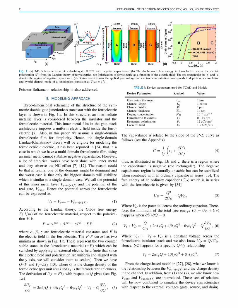
Fig. 2: The potential of middle metal versus the applied gate voltage fromthe analytical model (lines) and TCAD simulations (circles) for the variousthickness of ferroelectric from 2 nm to 12 nm (a) at VDS = 10 mV and(b) VDS = 1 V. By increasing the thickness of ferroelectric the voltageamplification increases.
By substituting (17) in (16) the integral in space turns into anintegral over the potential of the channel from the source (S)to the drain (D)
Q = −Qf2
+µ
2LgIds
∫ D
S
Q2mdVch. (18)
In depletion mode, dVch is obtained from (10) as follows
dVch =
(1
2Cox+
2UTQscQ2f −Q2
sc
+Qsc
4CscQf
)dQsc. (19)
Since dQsc = dQm, we introduce (19) in (18). After solvingthe integral, an analytical and explicit relation for the total
To
tal c
ha
rge
de
ns
ity
(C/m
2)
Vgate-∆𝜙ms (V)
VDS=10 mV
tf = 0, 2, 4, 6, 8, 10, 12 nm
Analytical model
TCAD
(a)
-0.5 0 0.5 1 1.5 2-0.02
0
0.02
0.04
0.06
0.08
0.1
-0.5 0 0.5 1 1.5 2-0.02
0
0.02
0.04
0.06
0.08
0.1
To
tal c
ha
rge
de
ns
ity
(C/m
2)
Vgate-∆𝜙ms (V)
VDS=1 V
tf = 0, 2, 4, 6, 8, 10, 12 nm
Analytical model
TCAD
(b)
Fig. 3: The total charge density in the ferroelectric versus the applied gatevoltage from the analytical model (lines) and TCAD simulations (circles) forthe various thickness of ferroelectric from 2 nm to 12 nm (a) at VDS =10 mV and (b) VDS = 1 V.
charge in the ferroelectric is obtained (in depletion mode):
Q = −Qf2
+µ
2LgIds
{Q3m
6Cox
+ 2UT
[QmQf −
Q2m
2− 2Q2
f ln(2Qf +Qm)
]+
Q4m
16CscQF+
Q3m
12Csc
}DS
.
(20)
In accumulation, we have
dVch =
(1
2Cox+
2UTQscQ2sc + θ
)dQsc. (21)
Substituting (21) in (18) and then solving the integral givesan analytical and explicit relationship for the total chargedensity of the ferroelectric when the whole device is biased
AMIN RASSEKH et al.: CHARGE-BASED MODELING NEGATIVE CAPACITANCE IN DG JUNCTIONLESS FETS 5
Dra
in c
urr
en
t (A
/µm
)
Vgate-∆𝜙ms (V)
VDS=10 mV
tf = 0, 8, 9, 10, 11, 12 nm
Analytical model
TCAD
(a)
Unstable region
-0.5 0 0.5 1 1.5 210
-9
10-8
10-7
10-6
10-5
10-4
10-3
10-2
-0.5 0 0.5 1 1.5 2
10-8
10-6
10-4
10-2
100
Dra
in c
urr
en
t (A
/µm
)
Vgate-∆𝜙ms (V)
VDS=1 V
tf = 0, 8, 9, 10, 11, 12 nm
Analytical model
TCAD
(b)
Unstable region
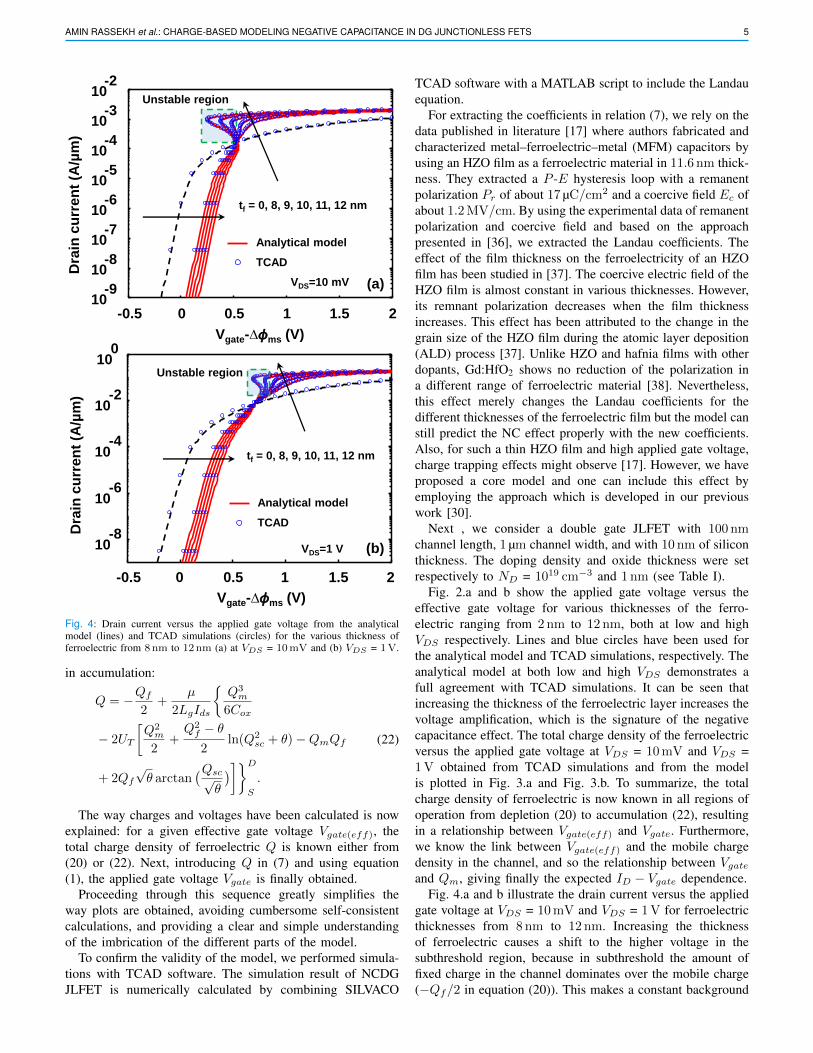
Fig. 4: Drain current versus the applied gate voltage from the analyticalmodel (lines) and TCAD simulations (circles) for the various thickness offerroelectric from 8 nm to 12 nm (a) at VDS = 10 mV and (b) VDS = 1 V.
in accumulation:
Q = −Qf2
+µ
2LgIds
{Q3m
6Cox
− 2UT
[Q2m
2+Q2f − θ2
ln(Q2sc + θ)−QmQf
+ 2Qf√θ arctan
(Qsc√θ
)]}DS
.
(22)
The way charges and voltages have been calculated is nowexplained: for a given effective gate voltage Vgate(eff), thetotal charge density of ferroelectric Q is known either from(20) or (22). Next, introducing Q in (7) and using equation(1), the applied gate voltage Vgate is finally obtained.
Proceeding through this sequence greatly simplifies theway plots are obtained, avoiding cumbersome self-consistentcalculations, and providing a clear and simple understandingof the imbrication of the different parts of the model.
To confirm the validity of the model, we performed simula-tions with TCAD software. The simulation result of NCDGJLFET is numerically calculated by combining SILVACO
TCAD software with a MATLAB script to include the Landauequation.
For extracting the coefficients in relation (7), we rely on thedata published in literature [17] where authors fabricated andcharacterized metal–ferroelectric–metal (MFM) capacitors byusing an HZO film as a ferroelectric material in 11.6 nm thick-ness. They extracted a P -E hysteresis loop with a remanentpolarization Pr of about 17 µC/cm2 and a coercive field Ec ofabout 1.2 MV/cm. By using the experimental data of remanentpolarization and coercive field and based on the approachpresented in [36], we extracted the Landau coefficients. Theeffect of the film thickness on the ferroelectricity of an HZOfilm has been studied in [37]. The coercive electric field of theHZO film is almost constant in various thicknesses. However,its remnant polarization decreases when the film thicknessincreases. This effect has been attributed to the change in thegrain size of the HZO film during the atomic layer deposition(ALD) process [37]. Unlike HZO and hafnia films with otherdopants, Gd:HfO2 shows no reduction of the polarization ina different range of ferroelectric material [38]. Nevertheless,this effect merely changes the Landau coefficients for thedifferent thicknesses of the ferroelectric film but the model canstill predict the NC effect properly with the new coefficients.Also, for such a thin HZO film and high applied gate voltage,charge trapping effects might observe [17]. However, we haveproposed a core model and one can include this effect byemploying the approach which is developed in our previouswork [30].
Next , we consider a double gate JLFET with 100 nmchannel length, 1 µm channel width, and with 10 nm of siliconthickness. The doping density and oxide thickness were setrespectively to ND = 1019 cm−3 and 1 nm (see Table I).
Fig. 2.a and b show the applied gate voltage versus theeffective gate voltage for various thicknesses of the ferro-electric ranging from 2 nm to 12 nm, both at low and highVDS respectively. Lines and blue circles have been used forthe analytical model and TCAD simulations, respectively. Theanalytical model at both low and high VDS demonstrates afull agreement with TCAD simulations. It can be seen thatincreasing the thickness of the ferroelectric layer increases thevoltage amplification, which is the signature of the negativecapacitance effect. The total charge density of the ferroelectricversus the applied gate voltage at VDS = 10 mV and VDS =1 V obtained from TCAD simulations and from the modelis plotted in Fig. 3.a and Fig. 3.b. To summarize, the totalcharge density of ferroelectric is now known in all regions ofoperation from depletion (20) to accumulation (22), resultingin a relationship between Vgate(eff) and Vgate. Furthermore,we know the link between Vgate(eff) and the mobile chargedensity in the channel, and so the relationship between Vgateand Qm, giving finally the expected ID − Vgate dependence.
Fig. 4.a and b illustrate the drain current versus the appliedgate voltage at VDS = 10 mV and VDS = 1 V for ferroelectricthicknesses from 8 nm to 12 nm. Increasing the thicknessof ferroelectric causes a shift to the higher voltage in thesubthreshold region, because in subthreshold the amount offixed charge in the channel dominates over the mobile charge(−Qf/2 in equation (20)). This makes a constant background
6 IEEE JOURNAL OF ELECTRON DEVICES SOCIETY, VOL. XX, NO. XX, XXXX 2020
(a)S
S (
mV
/dec)
Drain current (A/µm))
tf = 0, 8, 9 nm
SS=60 mV/dec
tf = 0, 8, 9, 10 nm
VDS=10 mV
10-9
10-8
10-7
10-6
10-5
55
60
65
70
75
80
85
90
95
100(b)
Sw
ing
(m
V/d
ec)
Drain current (A/µm)
VDS=10 mV
tf = 0, 8, 9 nm
SS=60 mV/dec
10-9
10-8
10-7
10-6
10-5
10-4
10-3
0
50
100
150
200
250
300
∆I D
/ID
0 [%
]
Vgate-∆𝜙ms (V)
tf = 0, 8, 9, 10, 11, 12
(c)
VDS=1 V
0 0.4 0.8 1.2 1.6 2-200
0
200
400
600
800
1000
1200
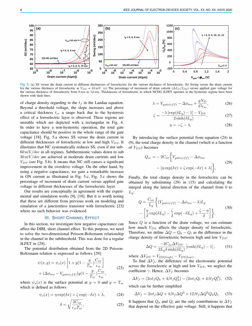
Fig. 5: (a) SS versus the drain current in different thicknesses of ferroelectric for the various thickness of ferroelectric. (b) Swing versus the drain currentfor the various thickness of ferroelectric at VDS = 10 mV. (c) The percentage of increment of drain current (∆ID/ID0) versus applied gate voltage forthe various thickness of ferroelectric from 8 nm to 12 nm. Thicknesses of ferroelectric in which NCDG JLFET operates in the hysteretic regime have beenshown with dash lines.
of charge density regarding to the tf in the Landau equation.Beyond a threshold voltage, the slope increases and abovea critical thickness tcr a snaps back due to the hysteresiseffect of a ferroelectric layer is observed. These regions areunstable which are depicted with a rectangular in Fig. 4.In order to have a non-hysteretic operation, the total gatecapacitance should be positive in the whole range of the gatevoltage [18]. Fig. 5.a shows SS versus the drain current indifferent thicknesses of ferroelectric at low and high VDS . Itillustrates that NC systematically reduces SS, even if not sub-60 mV/dec in all regimes. Subthermionic values down to sub30 mV/dec are achieved at moderate drain currents and lowVDS (see Fig. 5.b). It means that NC still causes a significantimprovement in the overdrive voltage. On the other hand, byusing a negative capacitance, we gain a remarkable increasein ON current as illustrated in Fig. 5.c. Fig. 5.c shows thepercentage of increment of drain current versus applied gatevoltage in different thicknesses of the ferroelectric layer.
Our results are conceptually in agreement with the experi-mental and simulation works [9], [18]. But it is worth notingthat these are different from previous work on modeling andsimulation of a junctionless transistor with ferroelectric [23]where no such behavior was evidenced.
III. SHORT CHANNEL EFFECT
In this section, we investigate how negative capacitance canaffect the DIBL short channel effect. To this purpose, we needto solve the two-dimensional Poisson-Boltzmann relationshipin the channel in the subthreshold. This was done for a regularJLFET in [29].
The potential distribution obtained from the 2D Poisson-Boltzmann relation is expressed as follows [29]:
ψ(x, y) = ψs(x)
[1 + y(1− y
Tsc)Coxεsi
]+ (∆φms − Vgate(eff))y(1− y
Tsc)Coxεsi
,
(23)
where ψs(x) is the surface potential at y = 0 and y = Tscwhich is defined as follows
ψs(x) = η exp(δx) + ζ exp(−δx) + λ, (24)
δ =
√2CoxεsiTsc
, (25)
λ = Vgate(eff) −∆φms +qNDδ2εsi
, (26)
ζ =−λ [exp(δLg)− 1]− VDS
2 sinh(δLg), (27)
η = −ζ − λ, (28)
By introducing the surface potential from equation (24) in(9), the total charge density in the channel (which is a functionof VDS) becomes
Qsc =− 2Cox
{Vgate(eff) −∆φms
− [η exp(δx) + ζ exp(−δx) + λ]
},
(29)
Finally, the total charge density in the ferroelectric can beobtained by substituting (29) in (15) and calculating theintegral along the lateral direction of the channel from 0 toLg:
Q =CoxLg
{(Vgate(eff) −∆φms − λ)Lg
−[η
δexp(δLg)−
ζ
δexp(−δLg) +
ζ − ηδ
]}.
(30)
Since Q is a function of the drain voltage, we can estimatehow much VDS affects the charge density of ferroelectric.Therefore, we define ∆Q = Qh −Ql as the difference in thecharge density of ferroelectric between high and low VDS :
∆Q =−2Cox∆VDS
2Lgδ sinh(δLg)[cosh(δLg)− 1] , (31)
where ∆VDS = VDS(high) − VDS(low).To find ∆Vf , the difference of the electrostatic potential
across the ferroelectric at high and low VDS , we neglect thecoefficient γ. Hence, ∆Vf becomes
∆Vf = (2αtfQh + 4βtfQ3h)− (2αtfQl + 4βtfQ
3l ), (32)
which can be further simplified
∆Vf = 2αtf∆Q+ 4βtf∆Q3 + 12βtf∆Q3QhQl. (33)
It happens that Qh and Ql are the only contributions to ∆Vfthat depend on the effective gate voltage. Still, it happens that

AMIN RASSEKH et al.: CHARGE-BASED MODELING NEGATIVE CAPACITANCE IN DG JUNCTIONLESS FETS 7
(a)
15 20 25 30 35 40 45 50-150
-100
-50
0
50
100
150
DIB
L(m
V/V
)
LG (nm)
tf = 0, 2, 4, 6, 8 nm
(b) (c)
tf = 2, 4, 6, 8 nm
15 20 25 30 35 40 45 500
50
100
150
200
250
-9
-8
-7
-6
-5
-4
-3
-2∆V
f (m
V)
LG (nm)
∆Q
(mC
/m2)
∆𝐕𝐟
𝐥𝐨𝐠(𝐈𝐃)
𝐕𝐆
𝐍𝐂𝐉𝐋𝐅𝐄𝐓 𝐡𝐢𝐠𝐡 𝐕𝐃𝐒
𝐍𝐂𝐉𝐋𝐅𝐓𝐄 𝐥𝐨𝐰 𝐕𝐃𝐒
𝐉𝐋𝐅𝐓𝐄 𝐡𝐢𝐠𝐡 𝐕𝐃𝐒
𝐉𝐋𝐅𝐓𝐄 𝐥𝐨𝐰 𝐕𝐃𝐒
Fig. 6: (a) The difference of the potential across the ferroelectric (left axis) and the difference of total charge density of ferroelectric (right axis) in high VDS
and low VDS versus the channel length. ∆Vf somehow represents ∆VG. The model confirms that ∆Vf and the absolute value of ∆Q increase by goingto the shorter channel length.(b) The schematic of the I-V characteristic of a regular double gate JLFET and a double gate JLFET with negative capacitanceat low and high VDS . (c) DIBL of an NCDG JLFET in different thicknesses of ferroelectric versus the channel length.
the last term in (33) containing these quantities is negligible,meaning that we can approximate ∆Vf as follows
∆Vf ≈ 2αtf∆Q+ 4βtf∆Q3. (34)
Fig. 6.a depicts ∆Vf and ∆Q versus the channel length onthe left and right axis respectively. We see that the absolutevalue of ∆Q increases by going to the shorter channel lengths,and as a result, ∆Vf increases as well. This is an advantagebecause it predicts that negative capacitance mitigates shortchannel effect at high VDS . Actually ∆Vf represents somehow∆VG, i.e. the difference of VG between high and low VDS .
The schematic drawing in Fig. 6.b illustrates this effect.It compares the I-V characteristic of a regular double gateJLFET and a double gate JLFET in presence of negativecapacitance at low and high VDS . As we mentioned in theprevious section, a negative capacitance causes a potentialamplification as much as Vf . Although Vf is almost the samefor high and low VDS for the long channel device, it becomesless effective at low VDS in regard to high VDS for a shortchannel device. In fact, in presence of short channel effect, theI-V characteristic that shifts towards high VDS is compensatedby ∆Vf in NCDG JLFET, thus DIBL reduction in a specificthickness of the ferroelectric film would be feasible.
Unlike conventional MOSFETs where DIBL is related tothe shift in the surface potential since most of the current flowfrom the Si-SiO2 interface, in JLFETs when they operate be-low the threshold, the interface no longer represents the lowesenergy across the channel and the DIBL must be calculatedfrom the center potential shift upon the drain voltage as follows[28], [29]
DIBL∆ψ =∆ψBCP,min
∆VDS, (35)
where ∆ψBCP,min is the difference of minimum body centerpotential in low and high VDS . We know from [28], [29] thatthe body center potential is linked to the surface potential:
ψBCP = aψs + b, (36)
where a and b coefficients are given by
a = 1 +1
8δ2T 2
sc, (37)
b = (a− 1)(∆φms − Vgate + Vf ). (38)
Therefore, the difference of body center potential of anNCJLFET in low and high VDS will be
∆ψBCP = a∆ψs + (a− 1)∆Vf . (39)
Then ∆ψs obtains from (9) as follows
∆ψs = −∆Vf +∆Qsc2Cox
. (40)
We can replace ∆Qsc with ∆QscJL+∆Q′sc where ∆QscJL
isthe difference of the total charge density in the semiconductorin a normal JLFET without NC. Hence, ∆ψs links to thedifference of the surface potential of a normal JLFET in lowand high VDS (∆ψsJL
= ∆QscJL/2Cox) as follows
∆ψs = ∆ψsJL−∆Vf +
∆Q′sc2Cox
. (41)
If we neglect ∆Q′sc/2Cox and introduce (41) in (39), we willhave (we know that ∆ψBCPJL
= a∆ψsJL)
∆ψBCP ≈ ∆ψBCPJL−∆Vf . (42)
Therefore, DIBL in NCJLFET shifts as much as ∆Vf/∆VDSrespect to the DIBL in a JLFET.
DIBL∆ψ ≈ DIBL∆ψJL− ∆Vf
∆VDS, (43)
where DIBL∆ψJLdefines as follows [28], [29]
DIBL∆ψJL=
2a√η′ζ ′
∆VDS
(√1 +
∆
η′− ∆
ζ ′− ∆2
η′ζ ′−1
), (44)
ζ ′ =(−b− aλ) [exp(δLg)− 1]− VDS
2a sinh(δLg), (45)
η = − ba− ζ ′ − λ, (46)
∆ =∆VDS
2a sinh(δLg). (47)
Fig. 6.c shows DIBL of an NCDG JLFET in differentthicknesses of ferroelectric versus the channel length. We seethat the value of DIBL decreases by increasing the thickness ofthe ferroelectric. As expected, in the short channel lengths, thedifferent amount of potential drops across the ferroelectric filmat low and high VDS which causes a reduction in the DIBL

8 IEEE JOURNAL OF ELECTRON DEVICES SOCIETY, VOL. XX, NO. XX, XXXX 2020
even to the negative values. Hence, it appears that by choosinga proper thickness for the ferroelectric film, an improvementin the DIBL would be achievable e.g. in our case tf≈3 nmgives the lowest DIBL. Further studies for an optimizationDIBL strategy and trade-offs with other performance figuresof merit are needed, which was beyond the scope of this paper.
IV. CONCLUSION
An analytical charge-based model for symmetric double-gate junctionless FETs with negative capacitance was de-veloped. The model incorporates the impact of the negativecapacitance of ferroelectric on DC electrical characteristics ofdouble gate JLFETs by proposing an analytical and explicitequation for the total charge density of ferroelectric in deple-tion and accumulation modes. The model confirms that usingthe negative capacitance in junctionless transistors means thatthe gate overdrive voltage decreases, which can be interpretedas lower energy consumption. The model also shows thatthe subthreshold slope almost remains constant in NCDGJLFET, but an improvement of swing for above the thresholdcauses a significant enhancement in ON current. In addition,an analysis of the short channel effect predicts an improvementwhen negative capacitance is observed. The model has beencompared to TCAD simulations with an excellent agreementin all regions of operation from deep depletion to accumulationand linear to saturation.
V. APPENDIXThe total polarization P can be expressed as the sum of a
linear and switching dipole PD contributions as follows [39]
P = ε0χE + PD. (48)
Hence, the surface charge density σ of ferroelectric becomes
σ = Vεftf
+ PD, (49)
where εf = ε0 (1 + χ). Thus the capacitance becomes
C =dσ
dV=
1
tf
(εf + tf
dPDdV
). (50)
We can replace dV with tfdE and then dPD/dE = dP/dE−ε0χ. Therefore, the capacitance is related to the slope of theP -E curve as expressed in (4).
ACKNOWLEDGEMENT
This work was financially supported by the European Re-search Council (ERC) under the ERC Advanced Grants Milli-Tech (695459 ERC Millitech).
REFERENCES
[1] N. Collaert, High Mobility Materials for CMOS Applications. Wood-head Publishing, 2018.
[2] R. Chau, “Process and packaging innovations for moore’s law continua-tion and beyond,” in 2019 IEEE International Electron Devices Meeting(IEDM). IEEE, 2019, pp. 1–1.
[3] K. E. Moselund, M. Najmzadeh, P. Dobrosz, S. H. Olsen, D. Bouvet,L. De Michielis, V. Pott, and A. M. Ionescu, “The high-mobility bendedn-channel silicon nanowire transistor,” IEEE transactions on electrondevices, vol. 57, no. 4, pp. 866–876, 2010.
[4] A. M. Ionescu, “Beyond-cmos low-power devices: Steep-slope switchesfor computation and sensing,” Nanoelectronics: Materials, Devices,Applications, 2 Volumes, 2017.
[5] C.-W. Lee, A. Afzalian, N. D. Akhavan, R. Yan, I. Ferain, and J.-P.Colinge, “Junctionless multigate field-effect transistor,” Applied PhysicsLetters, vol. 94, no. 5, p. 053511, 2009.
[6] S. Takagi, T. Iisawa, T. Tezuka, T. Numata, S. Nakaharai, N. Hirashita,Y. Moriyama, K. Usuda, E. Toyoda, S. Dissanayake et al., “Carrier-transport-enhanced channel cmos for improved power consumption andperformance,” IEEE Transactions on Electron Devices, vol. 55, no. 1,pp. 21–39, 2007.
[7] A. Rusu, G. A. Salvatore, D. Jimenez, and A. M. Ionescu, “Metal-ferroelectric-meta-oxide-semiconductor field effect transistor with sub-60mv/decade subthreshold swing and internal voltage amplification,” in2010 International Electron Devices Meeting. IEEE, 2010, pp. 16–3.
[8] A. M. Ionescu, “Sub-unity body factor: The next cmos and beyondcmos technology booster for enhanced energy efficiency?” in 2017 FifthBerkeley Symposium on Energy Efficient Electronic Systems & SteepTransistors Workshop (E3S). IEEE, 2017, pp. 1–3.
[9] A. Saeidi, F. Jazaeri, F. Bellando, I. Stolichnov, G. V. Luong, Q.-T.Zhao, S. Mantl, C. C. Enz, and A. M. Ionescu, “Negative capacitanceas performance booster for tunnel fets and mosfets: An experimentalstudy,” IEEE Electron Device Letters, vol. 38, no. 10, pp. 1485–1488,2017.
[10] A. Saeidi, F. Jazaeri, I. Stolichnov, C. C. Enz, and A. M. Ionescu,“Negative capacitance as universal digital and analog performancebooster for complementary mos transistors,” Scientific reports, vol. 9,no. 1, pp. 1–9, 2019.
[11] A. I. Khan, K. Chatterjee, B. Wang, S. Drapcho, L. You, C. Serrao,S. R. Bakaul, R. Ramesh, and S. Salahuddin, “Negative capacitance ina ferroelectric capacitor,” Nature materials, vol. 14, no. 2, pp. 182–186,2015.
[12] D. J. Appleby, N. K. Ponon, K. S. Kwa, B. Zou, P. K. Petrov, T. Wang,N. M. Alford, and A. O’Neill, “Experimental observation of negativecapacitance in ferroelectrics at room temperature,” Nano letters, vol. 14,no. 7, pp. 3864–3868, 2014.
[13] S. Salahuddin and S. Datta, “Use of negative capacitance to providevoltage amplification for low power nanoscale devices,” Nano letters,vol. 8, no. 2, pp. 405–410, 2008.
[14] A. M. Ionescu, L. Lattanzio, G. A. Salvatore, L. De Michielis, K. Bou-cart, and D. Bouvet, “The hysteretic ferroelectric tunnel fet,” IEEEtransactions on electron devices, vol. 57, no. 12, pp. 3518–3524, 2010.
[15] G. A. Salvatore, D. Bouvet, and A. M. Ionescu, “Demonstration ofsubthrehold swing smaller than 60mv/decade in fe-fet with p (vdf-trfe)/sio 2 gate stack,” in 2008 IEEE International Electron DevicesMeeting. IEEE, 2008, pp. 1–4.
[16] L. D. Landau, “On the theory of phase transitions,” Ukr. J. Phys., vol. 11,pp. 19–32, 1937.
[17] M. Hoffmann, F. P. Fengler, M. Herzig, T. Mittmann, B. Max,U. Schroeder, R. Negrea, P. Lucian, S. Slesazeck, and T. Mikolajick,“Unveiling the double-well energy landscape in a ferroelectric layer,”Nature, vol. 565, no. 7740, p. 464, 2019.
[18] A. Saeidi, F. Jazaeri, I. Stolichnov, and A. M. Ionescu, “Double-gatenegative-capacitance mosfet with pzt gate-stack on ultra thin body soi:An experimentally calibrated simulation study of device performance,”IEEE Transactions on Electron Devices, vol. 63, no. 12, pp. 4678–4684,2016.
[19] C. Jiang, R. Liang, J. Wang, and J. Xu, “A carrier-based analytical theoryfor negative capacitance symmetric double-gate field effect transistorsand its simulation verification,” Journal of Physics D: Applied Physics,vol. 48, no. 36, p. 365103, 2015.
[20] H. Mehta and H. Kaur, “Impact of gaussian doping profile and negativecapacitance effect on double-gate junctionless transistors (dgjlts),” IEEETransactions on Electron Devices, vol. 65, no. 7, pp. 2699–2706, 2018.
[21] Y. Choi, Y. Hong, and C. Shin, “Device design guideline for junctionlessgate-all-around nanowire negative-capacitance fet with hfo2-based fer-roelectric gate stack,” Semiconductor Science and Technology, vol. 35,no. 1, p. 015011, 2019.
[22] M. Gupta and V. P.-H. Hu, “Negative capacitance junctionless devicewith mid-gap work function for low power applications,” IEEE ElectronDevice Letters, vol. 41, no. 3, pp. 473–476, 2020.
[23] H. Mehta and H. Kaur, “Modeling and simulation study of noveldouble gate ferroelectric junctionless (dgfjl) transistor,” Superlatticesand microstructures, vol. 97, pp. 536–547, 2016.
[24] H. Ota, T. Ikegami, J. Hattori, K. Fukuda, S. Migita, and A. Toriumi,“Fully coupled 3-d device simulation of negative capacitance finfets for

AMIN RASSEKH et al.: CHARGE-BASED MODELING NEGATIVE CAPACITANCE IN DG JUNCTIONLESS FETS 9
sub 10 nm integration,” in 2016 IEEE International Electron DevicesMeeting (IEDM). IEEE, 2016, pp. 12–4.
[25] Z. Dong and J. Guo, “A simple model of negative capacitance fetwith electrostatic short channel effects,” IEEE Transactions on ElectronDevices, vol. 64, no. 7, pp. 2927–2934, 2017.
[26] J. Seo, J. Lee, and M. Shin, “Analysis of drain-induced barrier risingin short-channel negative-capacitance fets and its applications,” IEEETransactions on Electron Devices, vol. 64, no. 4, pp. 1793–1798, 2017.
[27] J.-M. Sallese, N. Chevillon, C. Lallement, B. Iniguez, and F. Pregaldiny,“Charge-based modeling of junctionless double-gate field-effect transis-tors,” IEEE Transactions on Electron Devices, vol. 58, no. 8, pp. 2628–2637, 2011.
[28] F. Jazaeri and J.-M. Sallese, Modeling Nanowire and Double-GateJunctionless Field-Effect Transistors. Cambridge University Press,2018.
[29] F. Jazaeri, L. Barbut, A. Koukab, and J.-M. Sallese, “Analytical modelfor ultra-thin body junctionless symmetric double gate mosfets insubthreshold regime,” Solid-State Electronics, vol. 82, pp. 103–110,2013.
[30] A. Rassekh, F. Jazaeri, M. Fathipour, and J.-M. Sallese, “Modelinginterface charge traps in junctionless fets, including temperature effects,”IEEE Transactions on Electron Devices, vol. 66, no. 11, pp. 4653–4659,2019.
[31] F. Jazaeri, L. Barbut, and J.-M. Sallese, “Generalized charge-basedmodel of double-gate junctionless fets, including inversion,” IEEETransactions on Electron Devices, vol. 61, no. 10, pp. 3553–3557, 2014.
[32] M. Shalchian, F. Jazaeri, and J.-M. Sallese, “Charge-based model forultrathin junctionless dg fets, including quantum confinement,” IEEETransactions on Electron Devices, vol. 65, no. 9, pp. 4009–4014, 2018.
[33] F. Jazaeri, L. Barbut, and J.-M. Sallese, “Modeling asymmetric operationin double-gate junctionless fets by means of symmetric devices,” IEEETransactions on Electron Devices, vol. 61, no. 12, pp. 3962–3970, 2014.
[34] M. Hoffmann, M. Pesic, S. Slesazeck, U. Schroeder, and T. Mikolajick,“Modeling and design considerations for negative capacitance field-effect transistors,” in 2017 Joint International EUROSOI Workshop andInternational Conference on Ultimate Integration on Silicon (EUROSOI-ULIS). IEEE, 2017, pp. 1–4.
[35] A. Rassekh and M. Fathipour, “A single-gate soi nanosheet junctionlesstransistor at 10-nm gate length: design guidelines and comparison withthe conventional soi finfet,” Journal of Computational Electronics, pp.1–9, 2020.
[36] D. Ricinschi, C. Harnagea, C. Papusoi, L. Mitoseriu, V. Tura, andM. Okuyama, “Analysis of ferroelectric switching in finite media asa landau-type phase transition,” Journal of Physics: Condensed Matter,vol. 10, no. 2, p. 477, 1998.
[37] M. Hyuk Park, H. Joon Kim, Y. Jin Kim, T. Moon, and C. Seong Hwang,“The effects of crystallographic orientation and strain of thin hf0. 5zr0.5o2 film on its ferroelectricity,” Applied Physics Letters, vol. 104, no. 7,p. 072901, 2014.
[38] M. Hoffmann, U. Schroeder, T. Schenk, T. Shimizu, H. Funakubo,O. Sakata, D. Pohl, M. Drescher, C. Adelmann, R. Materlik et al.,“Stabilizing the ferroelectric phase in doped hafnium oxide,” Journalof Applied Physics, vol. 118, no. 7, p. 072006, 2015.
[39] J.-M. Sallese and P. Fazan, “Switch and rf ferroelectric mems: a newconcept,” Sensors and Actuators A: Physical, vol. 109, no. 3, pp. 186–194, 2004.


![JOURNAL OF IEEE XXX XXX, VOL. XX, NO. XX, …1103.1439v3 [cs.IT] 10 Sep 2013 JOURNAL OF IEEE XXX XXX, VOL. XX, NO. XX, AUGUST 2010 1 Generating Functional Analysis for Iterative CDMA](https://static.fdocuments.us/doc/165x107/5af78a247f8b9a9e5990dd4a/journal-of-ieee-xxx-xxx-vol-xx-no-xx-11031439v3-csit-10-sep-2013-journal.jpg)