IDDQ Testing Outline - University of Cincinnatieecs.ceas.uc.edu/~wjone/iddq.pdf · IDDQ testing.27...
66
IDDQ testing.1 IDDQ Testing Outline ! Introduction ! Inductive Fault Analysis ! Faults That Can Be Detected ! Circuit Constrains ! Design and Test Rules ! ATPG for IDDQ Testing ! Current Monitoring Methods ! Built-in Current Sensors ! QTAG Standard ! Deep Sub-micron Issues ! Some Specific Examples ! Conclusions
Transcript of IDDQ Testing Outline - University of Cincinnatieecs.ceas.uc.edu/~wjone/iddq.pdf · IDDQ testing.27...

IDDQ testing.1
IDDQ Testing Outline! Introduction! Inductive Fault Analysis! Faults That Can Be Detected! Circuit Constrains! Design and Test Rules! ATPG for IDDQ Testing! Current Monitoring Methods! Built-in Current Sensors! QTAG Standard! Deep Sub-micron Issues! Some Specific Examples! Conclusions

IDDQ testing.2
IDDQ TestingIDD --- Current flow through VDDQ --- Quiescent stateIDDQ Testing --- Detecting faults by monitoring IDDQ
Normal IDDQ: ~10-9Amp.Abnormal IDDQ: >10-5Amp.
CMOScircuit
Inputs Outputs
VDD
IDD

IDDQ testing.3
Advantages of IDDQ Testing
" Fault effect is easy to detect" Many realistic faults are detectable" ATPG is relatively simple" Test length is shorter" Built-in current sensing is possible
IDDQ testing.4
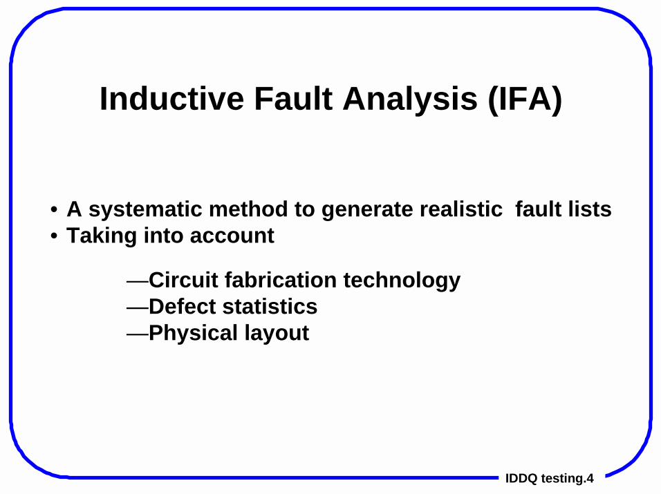
Inductive Fault Analysis (IFA)
• A systematic method to generate realistic fault lists• Taking into account
—Circuit fabrication technology—Defect statistics—Physical layout

IDDQ testing.5
Framwork of Inductive Fault AnalysisTechnology
Analysis
LayoutParsing
DefectGeneration
Primitive FaultExtraction
Circuit FaultTranslation
TechnologyDescription
CircuitLayout
DefectStatistics
Primitive FaultTaxonomy
Layout Data Structures
Defects
PrimitiveFault List
Ranked CircuitFault List
IDDQ testing.6
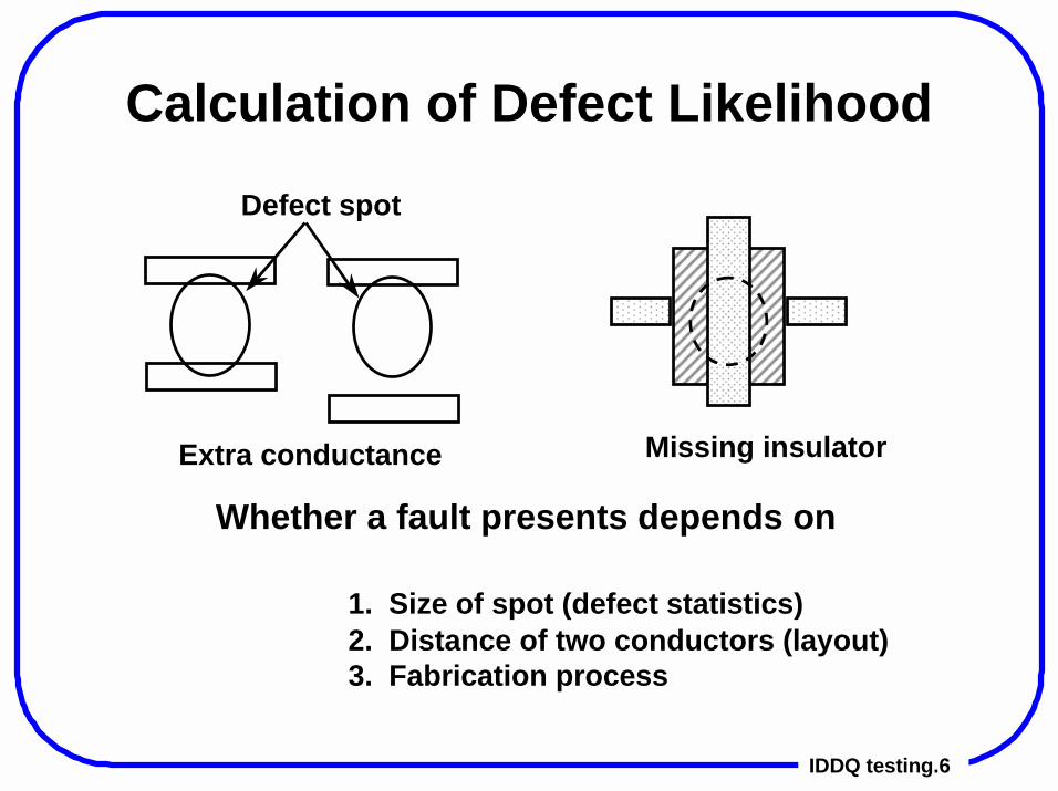
Calculation of Defect LikelihoodDefect spot
Extra conductance Missing insulator
Whether a fault presents depends on
1. Size of spot (defect statistics)2. Distance of two conductors (layout)3. Fabrication process

IDDQ testing.7
Defects in a Poly Path
(a) Defect-free poly path (b) insignificant missing poly
(d) significant missing poly(c) insignificant missing poly

IDDQ testing.8
Results of IFA�
Defect Type Fault Categories
pin- holes
miss. metal
extra metal
m iss. poly.
extra poly.
m iss. diff.
extra diff.
m iss. p-wel
l
extra p-wel
l
m iss. cont.
all def.
% of fault
s Bridges 42 - 61 - 52 - 8 31 35 - 229 48% Breaks - 82 - 78 1 10 - - - 9 180 38% Combin. - - - - 1 - - - - - 1 0.2% New T - - - - 2 - .1 - - - 2 0.4% T-SON - - - 62 - - - - - - 62 13% T-SOP - - - - - 0.5 - - - - .05 0% Except. - - - - - - 1 - - - 1 0.2%
(5,5,4)Counter
Defect Type Fault Categories
pin- holes
miss. metal
extra metal
m iss. poly.
extra poly.
m iss. diff.
extra diff.
m iss. p-wel
l
extra p-wel
l
m iss. cont.
all def.
% of fault
s Bridges 111 - 257 - 125 - 12 62 78 - 645 48% Breaks - 281 - 230 4 21 - - - 29 565 42% Combin. - - - 134 - - - - - - 134 10% New T - - - - 3 - .- - - - 3 0.2% T-SON - - - - 3 - <1 - - - 3 0.2% T-SOP - - - - - <1 - - - - <1 0% Except. - - - - - - 2 - - - 2 0.2%
4 x 4 Multiplier
Combin. : Both bridge and break presentT-SON(SOP): Transistor struck-on (stuck-open)New T : New transistor created

IDDQ testing.9
New Transistors
(A) Caused by extra poly (B) Missing thinox
diffusion

IDDQ testing.10
Faults That Can Be Detected
• Bridge & stuck-on faults
• Break faults— Line break— Gate break— Drain break— Source break
• Transistor stuck-open faults
• Other faults
IDDQ testing.11
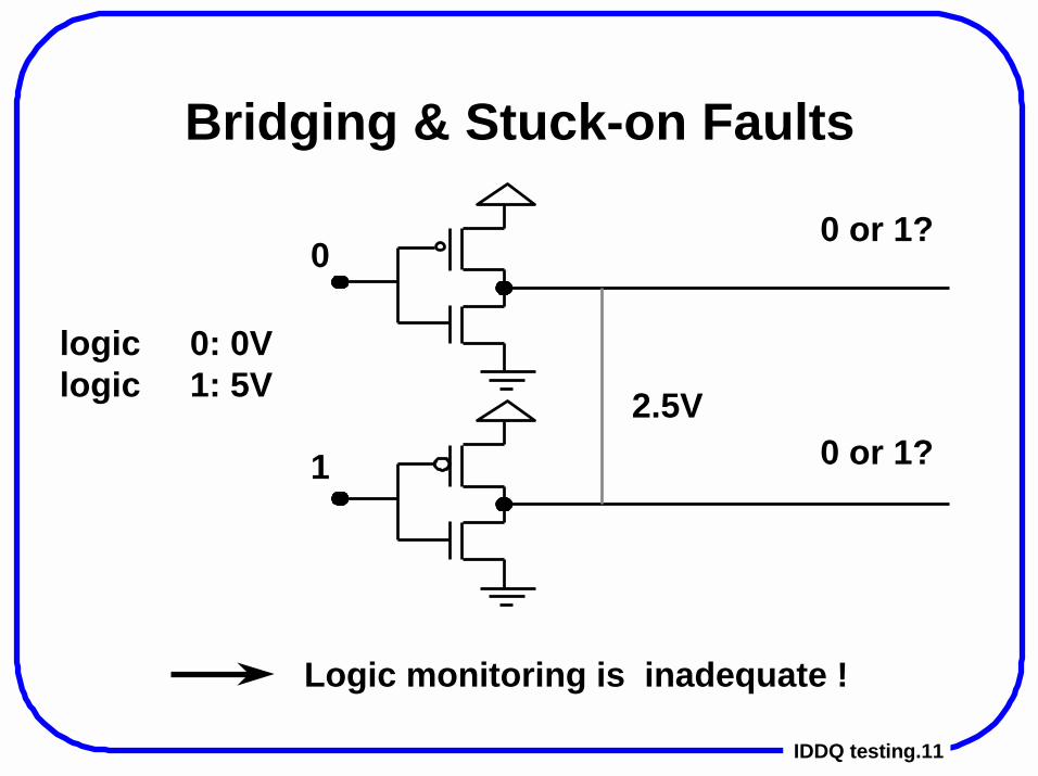
Bridging & Stuck-on Faults
Logic monitoring is inadequate !
logic 0: 0Vlogic 1: 5V
0
12.5V
0 or 1?
0 or 1?

IDDQ testing.12
Line Break Faults5V 5V
Induce large current
A floating node may drift to 1.5V~3.5Vand hence may turn on both PMOSand NMOS transistors
IDDQ testing.13
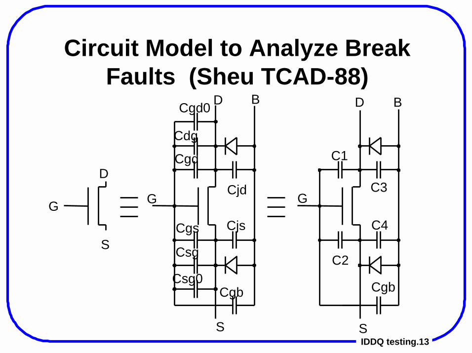
Circuit Model to Analyze BreakFaults (Sheu TCAD-88)
BCgd0
Cdg
Cgd
Cgs
Csg
Csg0
D
Cjd
Cjs
Cgb
G
D
S
D B
S S
C1
C2
GG
Cgb
C3
C4
IDDQ testing.14
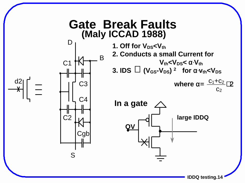
Gate Break Faults
B
S
D
C1
C3
C4
Cgb
C2
d2
In a gate large IDDQ
OV
1. Off for VDS<Vth2. Conducts a small Current for
Vth<VDS< α α α α.Vth3. IDS (VGS-VDS) 2 for αααα.vth<VDS
where α= ∼2α= ∼2α= ∼2α= ∼2c1+c2 c2
∝∝∝∝
(Maly ICCAD 1988)
IDDQ testing.15
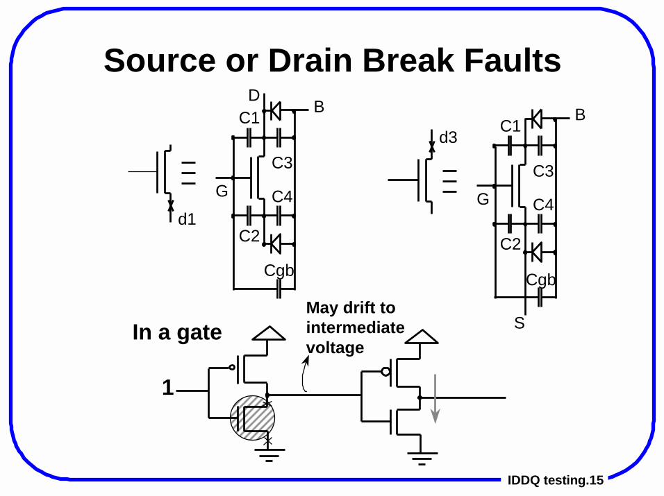
Source or Drain Break FaultsB
DC1
C3
C4
Cgb
C2d1
G
BC1
C3
C4
Cgb
C2
d3
G
SIn a gateMay drift tointermediatevoltage
1
IDDQ testing.16
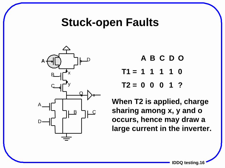
Stuck-open Faults
A B C D O
T1 = 1 1 1 1 0
T2 = 0 0 0 1 ?
When T2 is applied, chargesharing among x, y and ooccurs, hence may draw alarge current in the inverter.
B
C
x
y
D
O
CBA
D
A

IDDQ testing.17
Other Faults That Can Be Detected
• Gate-oxide short (Hawkins ITC85, D&T 86)• Most stuck-at faults (Fritzmeyer ITC-90)• Latch-up• Delay faults• Any other fault due to extra conductor, missing
isolating layer, excess well/substrate leakage,etc.

IDDQ testing.18
Circuit Constraints
To ensure IDDQ detectability, two conditionsmust be satisfied:
1. Normal IDDQ must be small
2. Faults must result in large IDDQ
IDDQ testing.19
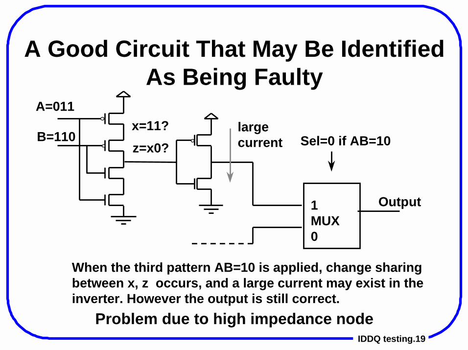
A Good Circuit That May Be IdentifiedAs Being Faulty
Problem due to high impedance node
x=11?z=x0?
1MUX0
Output
Sel=0 if AB=10
A=011
B=110
When the third pattern AB=10 is applied, change sharingbetween x, z occurs, and a large current may exist in theinverter. However the output is still correct.
largecurrent

IDDQ testing.20
A BF That Cannot Be Detected By IDDQ
Problem due to feedback loop
Φ=1: a=0, b=1Φ=1: Eventually x=y, no big current
Φ
Φ
Φ
Φ
Φ
Φ
a x
by
x
y
0
1

IDDQ testing.21
A BF That Is Masked By Another BF In aSequential Circuit
�
�
��
Φ� Φ�
Φ�
�
�
�
w
To detect (x,y) A=0, B=1, W=0
To set W=0, z must be 0 during Φ1
If (x,z) exists, then z will become 1 during Φ1

IDDQ testing.22
A BF That Is Masked By Another BF In aCombinational Circuit
A
B
C
w
z
x
y
A
O
To detect (x,y), we need A=0and z=0So we have to set ABC=1x1 first and then ABC=010If another fault (w,z) exists, then (x,y) cannot be detected
IDDQ testing.23
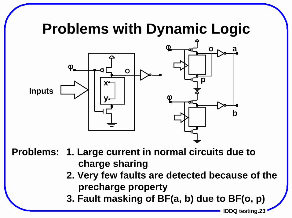
Problems with Dynamic Logic
Problems: 1. Large current in normal circuits due to charge sharing
2. Very few faults are detected because of the precharge property
3. Fault masking of BF(a, b) due to BF(o, p)
Inputsx
y
φφφφ
φφφφ
φφφφ
o a
b
pO

IDDQ testing.24
Transistor Group
Transistor group (TG) ---"Channel-connectedcomponent"
Connections between twoTGs are unidirectional
Control direction or loopcan be defined
A
B
C
D
Output G3 G2
G1
E
IDDQ testing.25
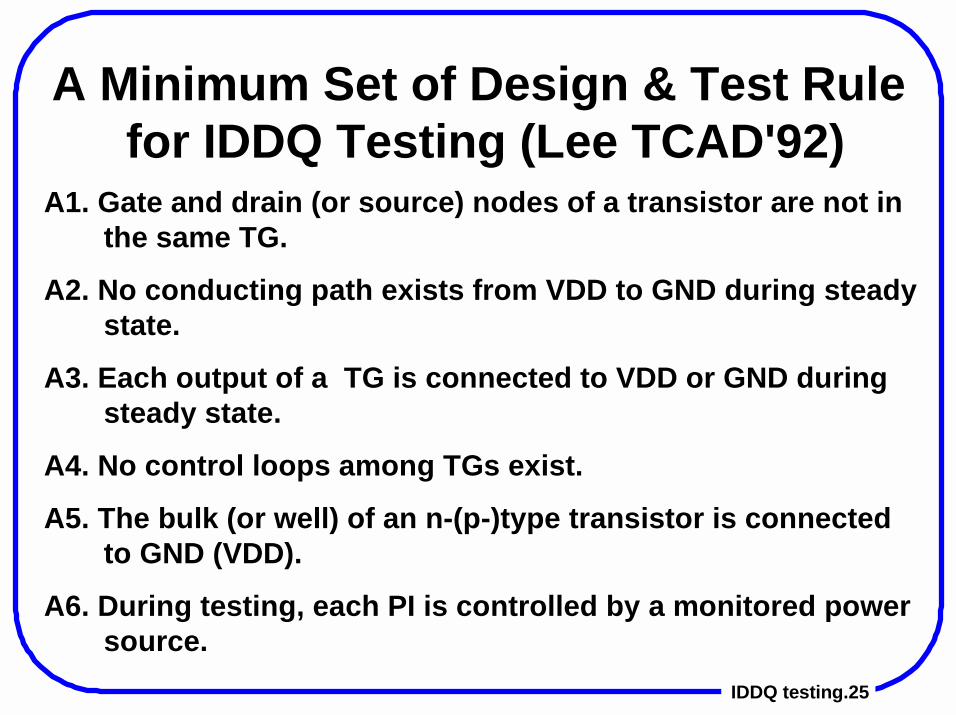
A Minimum Set of Design & Test Rule for IDDQ Testing (Lee TCAD'92)
A1. Gate and drain (or source) nodes of a transistor are not inthe same TG.
A2. No conducting path exists from VDD to GND during steadystate.
A3. Each output of a TG is connected to VDD or GND duringsteady state.
A4. No control loops among TGs exist.
A5. The bulk (or well) of an n-(p-)type transistor is connectedto GND (VDD).
A6. During testing, each PI is controlled by a monitored powersource.

IDDQ testing.26
Results of Design & Test RulesTheorem 1: All irredundant single BFs in a circuit satisfying
A1-A6 can be detected using IDDQ testing.
Theorem 2: For a circuit satisfying A1-A6, a test detecting asingle BF f also detects all multiple BFs thatcontain f.
Theorem 3: If any one of A1-A6 is removed, then circuitsexist for which IDDQ testing cannot give correcttest results.
Strategies for dealing with circuits not satisfying each ruleare required to ensure IDDQ detectability.

IDDQ testing.27
Fault Simulation1. Fault models --- Bridging, break, stuck-open,
stuck-at ?
2. Fault list generation --- need inductive faultanalysis
3. Fault coverage ?
4. Easy for bridging and stuck-on faults
5. Difficult for break and stuck-open faults
6. Stuck-at faults may or may not be modeled asshort to VDD or GND
IDDQ testing.28
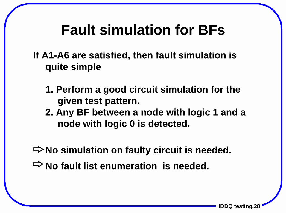
Fault simulation for BFsIf A1-A6 are satisfied, then fault simulation is
quite simple
1. Perform a good circuit simulation for the given test pattern.
2. Any BF between a node with logic 1 and a node with logic 0 is detected.
No simulation on faulty circuit is needed.No fault list enumeration is needed.
IDDQ testing.29
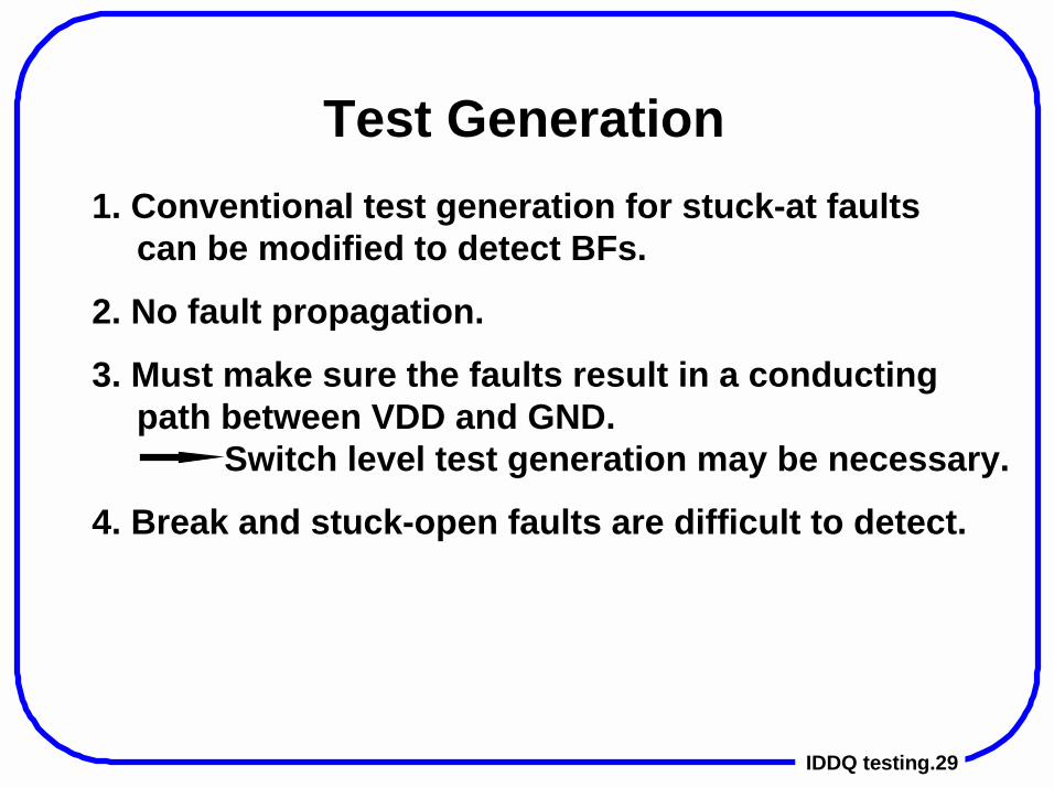
Test Generation1. Conventional test generation for stuck-at faults
can be modified to detect BFs.
2. No fault propagation.
3. Must make sure the faults result in a conductingpath between VDD and GND. Switch level test generation may be necessary.
4. Break and stuck-open faults are difficult to detect.
IDDQ testing.30
Test generator for BFs
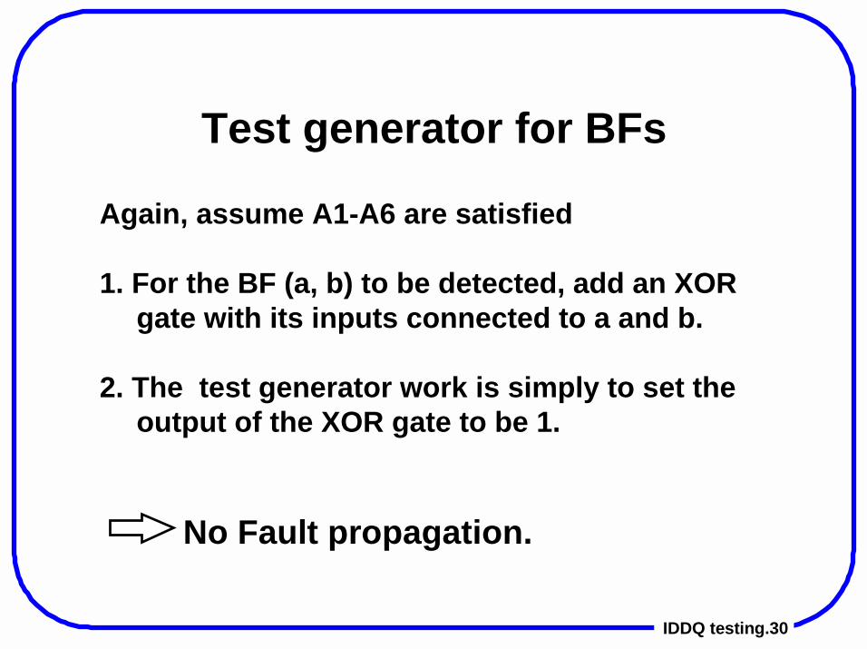
Again, assume A1-A6 are satisfied
1. For the BF (a, b) to be detected, add an XORgate with its inputs connected to a and b.
2. The test generator work is simply to set theoutput of the XOR gate to be 1.
No Fault propagation.
IDDQ testing.31
Test Length Using IDDQ Testing for BFs
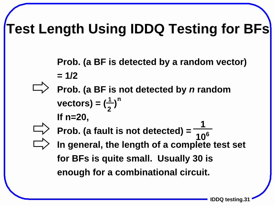
Prob. (a BF is detected by a random vector) = 1/2 Prob. (a BF is not detected by n random vectors) = ( ) If n=20, Prob. (a fault is not detected) = In general, the length of a complete test set for BFs is quite small. Usually 30 is enough for a combinational circuit.
12
n
1061

IDDQ testing.32
Comparison Between IDDQ and Logic Testing
#faults IDDQ Testing Fault Coverage(%) Logic Testing
Circuit (reduced) 4 vec. 8 vec. 12 vec. 16 vec. 20 vec. time(s) #vec. FC Time(m)
c432 263 97.65 99.62 99.96 - - 4.04 50 79 11.4
c499 284 97.46 98.93 99.37 99.62 99.73 9.15 184 87 30.5
c1908 617 97.24 98.82 99.32 99.59 99.75 21.4 138 84.8 28.6
s386 350 93.1 96.78 98.00 98.74 99.07 7.51 288 75 28.6
s526 1337 94.48 97.04 98.15 98.63 98.95 11.9 192 18.8 56.1
s832 680 91.78 95.64 97.23 98.15 98.54 18.8 967 75.7 3.08
IDDQ testing.33
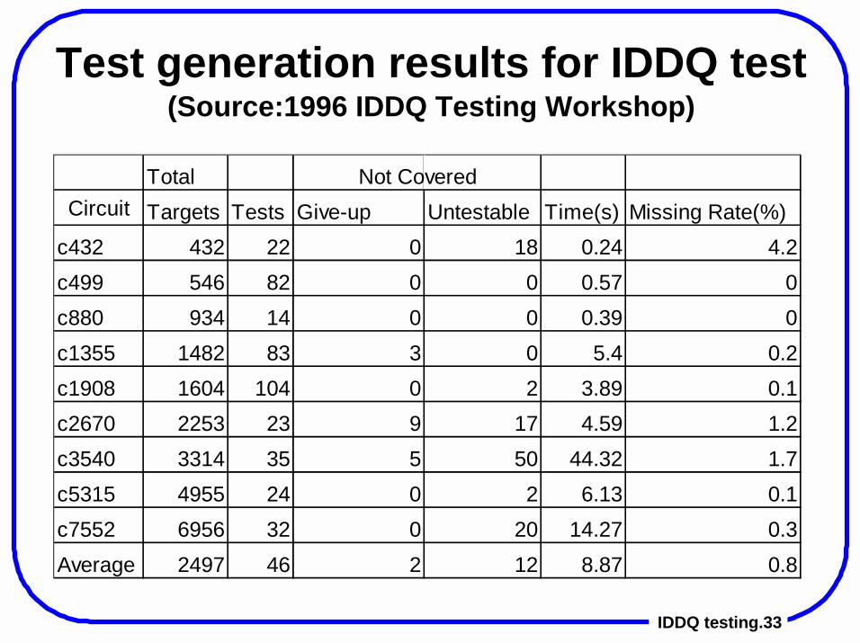
Test generation results for IDDQ test(Source:1996 IDDQ Testing Workshop)
Total Not CoveredCircuit Targets Tests Give-up Untestable Time(s) Missing Rate(%)
c432 432 22 0 18 0.24 4.2c499 546 82 0 0 0.57 0c880 934 14 0 0 0.39 0c1355 1482 83 3 0 5.4 0.2c1908 1604 104 0 2 3.89 0.1c2670 2253 23 9 17 4.59 1.2c3540 3314 35 5 50 44.32 1.7c5315 4955 24 0 2 6.13 0.1c7552 6956 32 0 20 14.27 0.3Average 2497 46 2 12 8.87 0.8
IDDQ testing.34
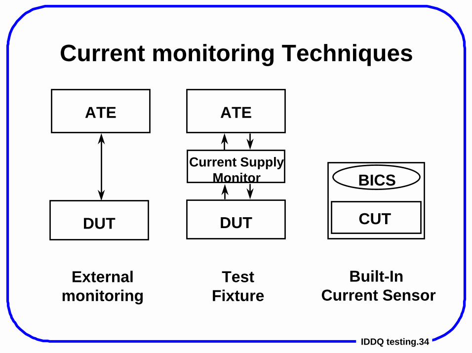
Current monitoring Techniques
CUT
BICSCurrent Supply
Monitor
DUTDUT
ATEATE
Externalmonitoring
TestFixture
Built-In Current Sensor

IDDQ testing.35
External Devices (Hawkins 86, 89)
Problems:
1. Current resolution is limitted. 2. Test equipment must be modified. 3. Current cannot be measured at the full speed of the tester. 4. Cannot partition circuit.
TEST POWER SUPPLY
S (STROBE)
NCNIDD
DUT
VSS pin
VDD pinVDD
RM

IDDQ testing.36
Built-in Current Sensors (BICSs)
BICS
CUT
Test Pass/Fail
VDD
Inputs Outputs
OR
CUT
BICS
Inputs Outputs
Test Pass /Fail
VDD
Sometimes called ISSQ testing

IDDQ testing.37
BICS Based on Bipolar Transistor and DifferentialAmplifier (Maly, ICCAD '88)
Pass/FailFlag
VR
VDD
φ1
φ2
φ1
CMOSModule
VirtualGround
Switchingcircuit
CMOS
Module
VDD
+ -
GNDI
VVR
VDD-GND Shorts
VR
NOdefect Defect
V
Shorts causingstruck-at faults
Shorts causingbridging faults & oxide pin-holes
Junctionleakages
NO defect
When large IDDQ exists, V>VR and Failflag is set.
The switching circuit may switch off afaulty module to prevent large powerconsumption
V

IDDQ testing.38
BICS Based on Logic ThresholdFavalli (JSSC-90)
Pull-up
Pull-down
Pull-up
Pull-down
Pull-up
Pull-down
MTt
Gnd
MTD
Gnd
MT
MTD
MT
MTD
Gnd
tout
VDD VDD VDD
inputs ...
...
...
Normal : t = 1Test : t = 0tout = 1 if no fault = 0 if fault exists
IDDQ testing.39
Improvement on Favalli's design
Pull-up
Pull-down
Pull-up
Pull-down
Pull-up
Pull-down
MT
MTD
Gnd
tout
VDD VDD VDD
inputs ...
...t
Merge all MT and MTDrespectively
IDDQ testing.40
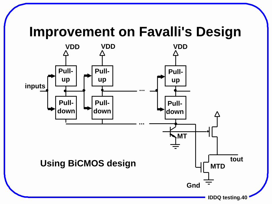
Using BiCMOS design
Pull-up
Pull-down
Pull-up
Pull-down
Pull-up
Pull-down
MT
MTD
Gnd
tout
VDD VDD VDD
inputs ...
...
Improvement on Favalli's Design
IDDQ testing.41
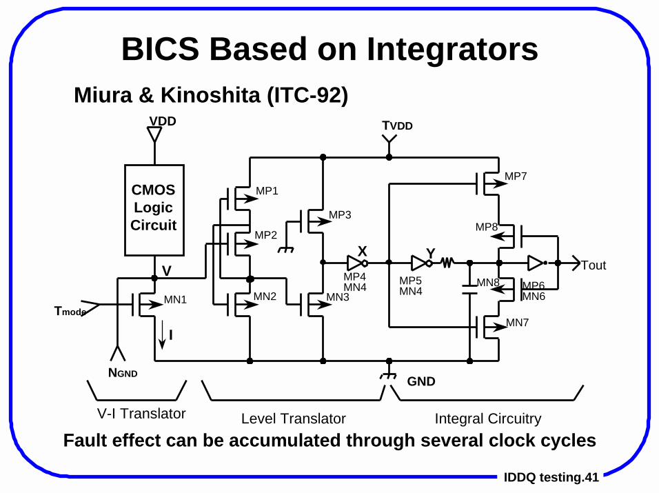
BICS Based on IntegratorsMiura & Kinoshita (ITC-92)
CMOSLogicCircuit
VDD TVDD
Tmode
NGND GND
MN1
MP2
MP1
MN2
MP3
MN3MP5MN4
MP4MN4 MN8
MN7
MP8
MP7
MP6MN6
Tout
V-I Translator Level Translator Integral CircuitryFault effect can be accumulated through several clock cycles
I
VX Y
IDDQ testing.42
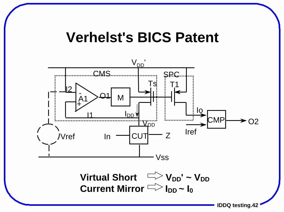
Verhelst's BICS Patent
O2
Vss
Vref
-+
I2
I1
O1 M
In Z IrefCMP
SPCCMSVDD'
A1
CUT
Ts T1
Virtual Short VDD' ~ VDDCurrent Mirror IDD ~ I0
IDDVDD
Io

IDDQ testing.43
BICS Based on Dual Power Supply &Operational Amplifier
-
+
Vin=3V Threshold detector
Fault indication
CUT
VDD=3V
RS
Vout+ Vout-
VDD'=5V
VSS
I-
I+
VirtualShort
IRS
IDD
Virtual short VDD~VinInfinite input impedance of OP I-=0 and IRS=IDD
IDDQ testing.44
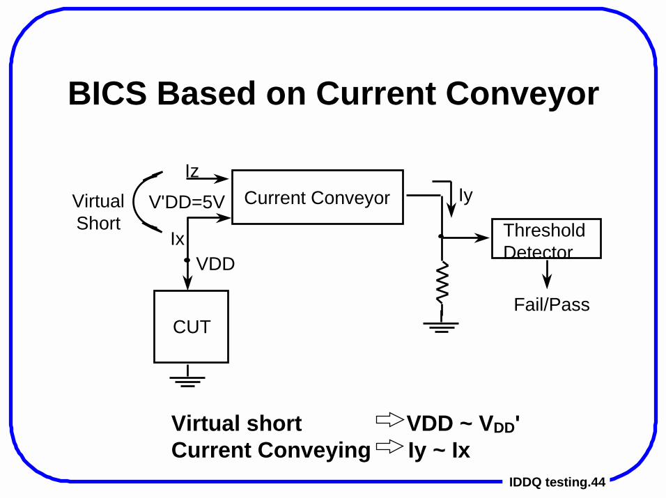
BICS Based on Current Conveyor
VirtualShort
V'DD=5VIz
IxVDD
CUT
Current Conveyor Iy
Fail/Pass
ThresholdDetector
Virtual short VDD ~ VDD'Current Conveying Iy ~ Ix

IDDQ testing.45
Advantages of Built-In Current Sensors(BICS)
• Higher test rate compared to external devices
• Easier to partition circuits
• Easier to control current resolution
• Suitable for mixed-mode circuits
• Built-In self test capability achievable
• Lower test equipment cost
• On-Line testing possible

IDDQ testing.46
Disadvantages of BICS
• Impact on circuit performance
• Reliability of itself
• Area overhead
• Power consumption
IDDQ testing.47
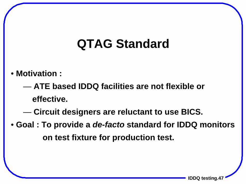
QTAG Standard
• Motivation :— ATE based IDDQ facilities are not flexible or effective.— Circuit designers are reluctant to use BICS.
• Goal : To provide a de-facto standard for IDDQ monitors on test fixture for production test.

IDDQ testing.48
Partnership of QTAG
• Semicoductor test department:Users, must drive the standard
•ATE Vendors:must supply the software to operate themonitors from ATE
•Test Fixture Vendors:must provide a small area close to CUT on alltest fixtures to mount the monitors.
•Monitor Developers:must supply the desired monitors.

IDDQ testing.49
Development of the Standard• Kick-off meeting at ITC’95, define 4 development phases --- phase 1: Monitor standard definition --- phase 2: Monitor design --- phase 3: Monitor evaluation --- phase 4: Working toward a standard• Results are reported in 4 papers presented in ITC’94• 1994 OCIMU (off-chip measurement unit) was developed by Alcatel• in 1995 ITC, the Monitor Description Format(MDF) language is presented• 1996 OCIMU POCIMU (threshold programmable)
IDDQ testing.50
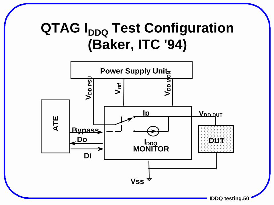
QTAG IDDQ Test Configuration(Baker, ITC '94)
Ip
IDDQMONITOR
Vss
DUT
ATE
Power Supply Unit
Do
Di
Bypass
V DD
PSU
V DD
MO
N
V ref
VDD DUT

IDDQ testing.51
QTAG Monitor on a Probe Card123
4 567
8
Power QTAG Monitor
Power Ring
Probe Nails
Control
10 cm

IDDQ testing.52
An example of Interface to Digital ATE
MO
NIT
OR
Vss
DUT
ATE
Power Supply Unit
V DD
PSU
V DD
mon
itor
1
3
6
4
8
2 7Sample
Threshold
Pass-Fail
On-Off
VDDdevicePIN FunctionVDDdevice to device under testVDDpsu to power supply VDDmonitor to secondary power source for monitorVSS group pin
Logic output indicate result of samplePass/fail High-level: under threshold when last sampled
Low-level: above threshold when last sampledSample Positive clock edge to indicate sampling point
On is the monitoring modeON-OFF OFF stops monitoring, but gives low Ohms pat
VDDpsu to VDDdeviceThreshold Sets threshold limit for P/F as input voltage lev

IDDQ testing.53
Circuit Diagram of IDUNA-1monitor
CUT
+
-
A2
Iout
T2
T3
T1T11
T10
T9T7 T8
T5 T6VREF
VSS VDM

IDDQ testing.54
IrefInternal Output
Bypass Front Back
Device under testVDD
VSS
VDD_MON
KICK
VDD_PSU
BYPASS
VREF 1
9
12
7
5
IREF DI TRIGGER
DO
NC
8 3 6
2
10
411
100nF VSS
Top-level Block Diagram of IDUNA II
IDDQ testing.55
+-
+-
VDD_PSU
VREF
IREF
VSS
VDD_DUT iddq/2
op_1
op_2
p1p2
p3
NICNIA NIB
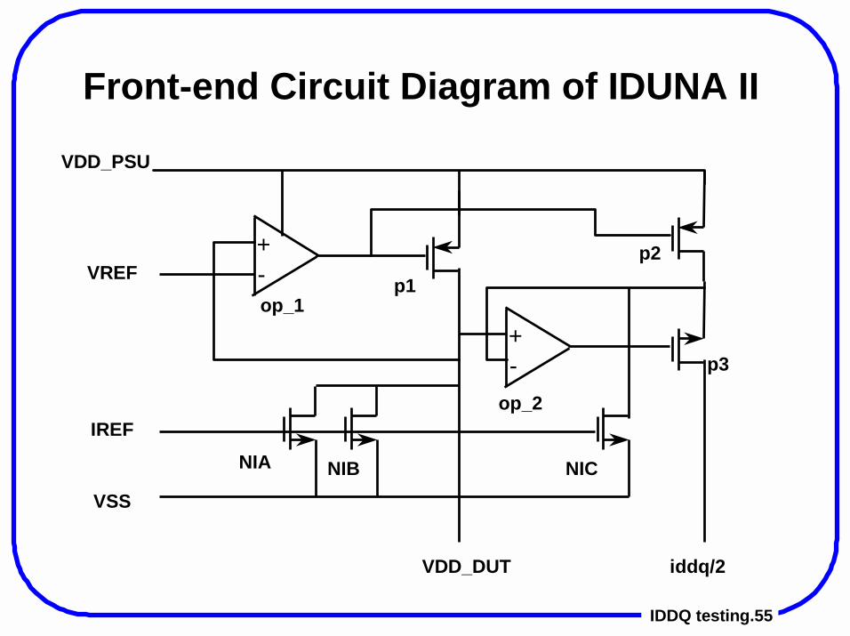
Front-end Circuit Diagram of IDUNA II
IDDQ testing.56
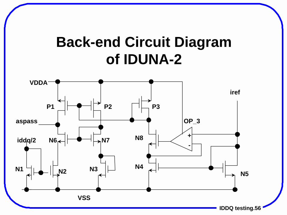
Back-end Circuit Diagramof IDUNA-2
iref
OP_3
+-
N5N4
N8
P3P1 P2
N6
N2N1
VSS
aspass
iddq/2
VDDA
N3
N7

IDDQ testing.57
Companies with Members in QTAG
AMD Ericson NECAT&T GEC PhilipsATTEST HP Sandia Lab.BNR Intel SchlumbergerBosch ITT SequentBrooktree LIRM SiemensChips&Technologies LTX SunCadence MCT SynopsysCredence Megatest TeradyneCrossCheck Motorola TIDigital National Semicon. Vertex
IDDQ testing.58
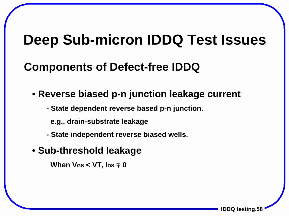
Deep Sub-micron IDDQ Test Issues
• Reverse biased p-n junction leakage current- State dependent reverse based p-n junction.
e.g., drain-substrate leakage
- State independent reverse biased wells.
• Sub-threshold leakage When VGS < VT, IDS = 0
Components of Defect-free IDDQ
\

IDDQ testing.59
Sub-Threshold Leakage Current
• When VGS < VT, IDS is an exponential function of (VGS-VT)
• Define�����
��
��
���
��
����
−= the inverse rate of decrease
of IDS in volts per decade
Typically S=80 ��������
IDDQ testing.60
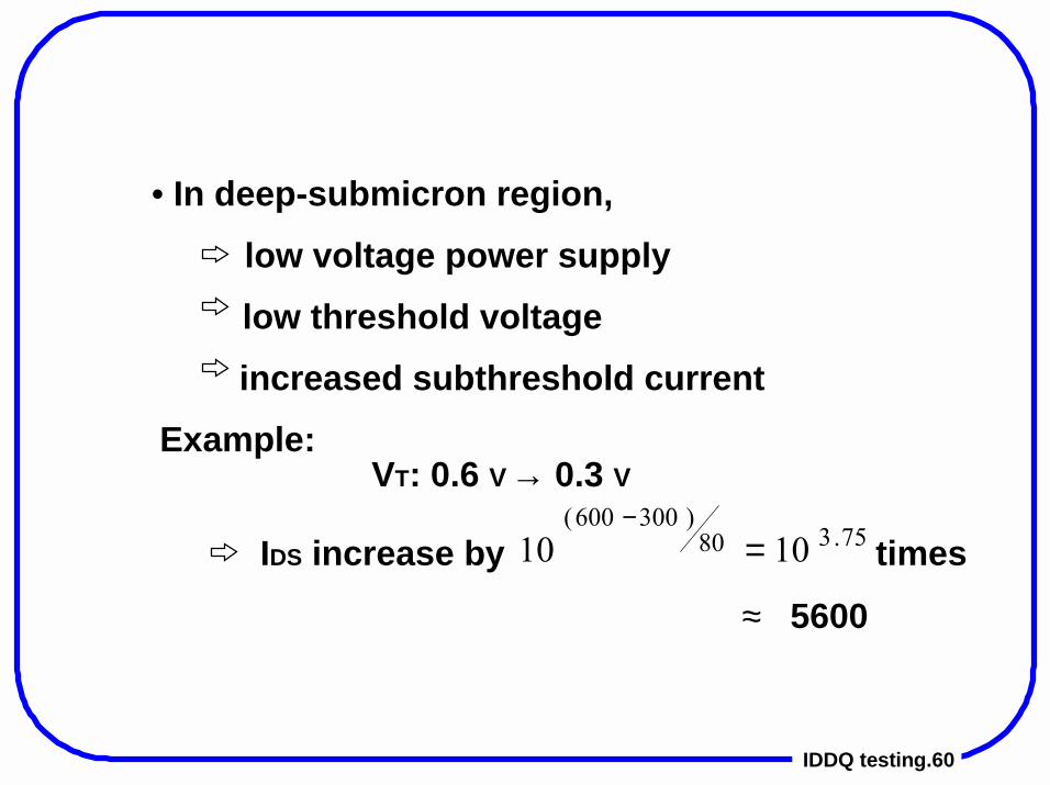
• In deep-submicron region,low voltage power supplylow threshold voltageincreased subthreshold current
Example:VT: 0.6 V→ 0.3 V
IDS increase by �������������
���� =−
times
≈ 5600

IDDQ testing.61
Deep Sub-micron IDDQ test Options
•Technology solution
•Technology solution
•Technology solution
Ex: Silicon On Insulator (SOI) sharper sub-threshold current slope
Ex: Separate Source and substrate connection in the test mode
Ex: Hierarchical power-line distribution with multiplethreshold transistors
Switched-Source impedcance (can reduce IDS to 0.3% of its original value, very useful in Giga-bit DRAM)
IDDQ testing.62
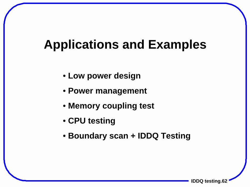
Applications and Examples
• Low power design
• Power management
• Memory coupling test
• CPU testing
• Boundary scan + IDDQ Testing

IDDQ testing.63
Applications of IDDQ and IDDT Testings������
���
����
���
������
�����
���
�� ����������
���������
�������
������
���������
� �����������
�����
�����������
����
���
����! ����! ����!
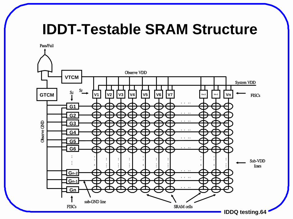
IDDQ testing.64
Vn-2V6V3
Gn-2
VTCM
GTCM
G1
G2G3
G4
G5G6
Gn-1
Gn
V1 V2 V4 V5 V7 Vn-1 Vn
��������������������
������� �
������� �
������� �
������� �
����������������������������������������
����������������������������
��������������������
��������������������
����������������������������������������
������������������������������������
������������������������������������
������������
����� ����������� ����������� ����������� ������
IDDT-Testable SRAM Structure

IDDQ testing.65
Some Experimental Results(for a Dynamic Combinational logic)
Total Defect Coverages(%)
Tested IDDQ IDDT IDDQ+IDDT Transition Test
Open drain/source 128 28.1 96.9 100 72.7
single floating gate 56 92.9 100 100 64.3
double floating gate 44 90.9 100 100 90.6
Short defects in the precharge chips 8 0 100 100 100

IDDQ testing.66
Conclusions
• Extremely important to achieve high-quality test.
• BICS can be either extremely profitable or nothing.
• ATPG for faults other than BFs needs further research.
• Deep sub-micron issues have to be addressed.