
ICs for Communications - Digi-Key Sheets/Infineon... · ICs for Communications ISDN...
320
ICs for Communications ISDN SubscribernAccess Controller ISAC .-S PEB 2085 PEB 2086 User’s Manual 10.94
Transcript of ICs for Communications - Digi-Key Sheets/Infineon... · ICs for Communications ISDN...

ICs for Communications
ISDN SubscribernAccess ControllerISAC.-S
PEB 2085
PEB 2086
User’s Manual 10.94

Data Classification
Maximum Ratings
Maximum ratings are absolute ratings; exceeding only one of these values may causeirreversible damage to the integrated circuit.
Characteristics
The listed characteristics are ensured over the operating range of the integrated circuit.Typical characteristics specify mean values expected over the production spread. If nototherwise specified, typical characteristics apply at TA = 25 °C and the given supply voltage.
Operating Range
In the operating range the functions given in the circuit description are fulfilled.
For detailed technical information about “Processing Guidelines” and “QualityAssurance” for ICs, see our “Product Overview” .
Edition 10.94This edition was realized using the software system FrameMaker.Published by Siemens AG, Bereich Halbleiter, Marketing-Kommunikation,Balanstraße 73, D-81541 München.
© Siemens AG 1994. All Rights Reserved.
As far as patents or other rights of third parties are concerned, liability is only assumed for components, not for applications, processes and circuits implemented within components or assemblies.
The information describes the type of component and shall not be considered as assured characteristics.
Terms of delivery and rights to change design reserved.
For questions on technology, delivery and prices please contact the Semiconductor Group Offices in Germany or the Siemens Companies and Representatives worldwide (see address list).
Due to technical requirements components may contain dangerous substances. For information on the types in question please contact your nearest Siemens Office, Semiconductor Group.
Siemens AG is an approved CECC manufacturer.
Packing
Please use the recycling operators known to you. We can also help you - get in touch with your nearest sales office. By agreement we will take packing material back, if it is sorted. You must bear the costs of transport.
For packing material that is returned to us unsorted or which we are not obliged to accept, we shall have to in-voice you for any costs incurred.
PEB 2085/PEB 2086 Revision History: 10.94
Previous Releases: 11.88; 3.89; 12.89; 02.95
Page Subjects (changes since last revision)
The present documentation is an editorial update of the Technical Manual 12.89
General Information
Table of Contents Page
1 Features . . . . . . . . . . . . . . . . . . . . . . . . . . . . . . . . . . . . . . . . . . . . . . . . . . . . . . . . . 10
1.1 Features of PEB 2085 . . . . . . . . . . . . . . . . . . . . . . . . . . . . . . . . . . . . . . . . . . . . . . 10
1.1.1 Pin Definitions and Functions of PEB 2085 . . . . . . . . . . . . . . . . . . . . . . . . . . . . . . 12
1.1.2 Logic Symbol of PEB 2085 . . . . . . . . . . . . . . . . . . . . . . . . . . . . . . . . . . . . . . . . . . 16
1.2 Features of PEB 2086 . . . . . . . . . . . . . . . . . . . . . . . . . . . . . . . . . . . . . . . . . . . . . . 17
1.2.1 Pin Definitions and Functions of PEB 2086 . . . . . . . . . . . . . . . . . . . . . . . . . . . . . . 19
1.2.2 Logic Symbol of PEB 2086 . . . . . . . . . . . . . . . . . . . . . . . . . . . . . . . . . . . . . . . . . . 23
1.3 Functional Block Diagram . . . . . . . . . . . . . . . . . . . . . . . . . . . . . . . . . . . . . . . . . . . 24
1.4 System Integration . . . . . . . . . . . . . . . . . . . . . . . . . . . . . . . . . . . . . . . . . . . . . . . . . 25
1.4.1 ISDN Applications . . . . . . . . . . . . . . . . . . . . . . . . . . . . . . . . . . . . . . . . . . . . . . . . . 25
1.4.2 Microprocessor Environment . . . . . . . . . . . . . . . . . . . . . . . . . . . . . . . . . . . . . . . . . 28
2 Functional Description . . . . . . . . . . . . . . . . . . . . . . . . . . . . . . . . . . . . . . . . . . . . . 31
2.1 General Functions and Device Architecture . . . . . . . . . . . . . . . . . . . . . . . . . . . . . 31
2.2 Interface and Operating Modes . . . . . . . . . . . . . . . . . . . . . . . . . . . . . . . . . . . . . . . 32
2.2.1 IOM®-1 Interface Mode (ADF2:IMS=0) . . . . . . . . . . . . . . . . . . . . . . . . . . . . . . . . . 32
2.2.2 IOM®-2 Interface Mode (ADF2:IMS=1) . . . . . . . . . . . . . . . . . . . . . . . . . . . . . . . . . 36
2.3 IOM®-1 Mode Functions . . . . . . . . . . . . . . . . . . . . . . . . . . . . . . . . . . . . . . . . . . . . 40
2.3.1 IOM®-1 Frame Structure / Timing Modes . . . . . . . . . . . . . . . . . . . . . . . . . . . . . . . 40
2.3.2 IOM®-1 Interface Connections . . . . . . . . . . . . . . . . . . . . . . . . . . . . . . . . . . . . . . . . 43
2.3.3 SLD Interface . . . . . . . . . . . . . . . . . . . . . . . . . . . . . . . . . . . . . . . . . . . . . . . . . . . . . 44
2.3.4 SSI (Serial Port A) . . . . . . . . . . . . . . . . . . . . . . . . . . . . . . . . . . . . . . . . . . . . . . . . . 46
2.3.5 B-Channel Switching . . . . . . . . . . . . . . . . . . . . . . . . . . . . . . . . . . . . . . . . . . . . . . . 47
2.3.6 mP Access to B Channels . . . . . . . . . . . . . . . . . . . . . . . . . . . . . . . . . . . . . . . . . . . 48
2.3.7 MONITOR Channel Handling . . . . . . . . . . . . . . . . . . . . . . . . . . . . . . . . . . . . . . . . 54
2.3.8 Command/Indicate (C/I) Channel Handling . . . . . . . . . . . . . . . . . . . . . . . . . . . . . . 55
2.4 IOM®-2 Mode Functions . . . . . . . . . . . . . . . . . . . . . . . . . . . . . . . . . . . . . . . . . . . . 58
2.4.1 IOM®-2 Frame Structure / Timing Modes . . . . . . . . . . . . . . . . . . . . . . . . . . . . . . . 58
2.4.2 IOM®-2 Interface Connections . . . . . . . . . . . . . . . . . . . . . . . . . . . . . . . . . . . . . . . . 61
2.4.3 mP Access to B and IC Channels . . . . . . . . . . . . . . . . . . . . . . . . . . . . . . . . . . . . . 68
2.4.4 MONITOR Channel Handling . . . . . . . . . . . . . . . . . . . . . . . . . . . . . . . . . . . . . . . . 71
Semiconductor Group 3

General Information
Table of Contents Page
2.4.5 C/I Channel Handling . . . . . . . . . . . . . . . . . . . . . . . . . . . . . . . . . . . . . . . . . . . . . . . 74
2.4.6 TIC Bus Access . . . . . . . . . . . . . . . . . . . . . . . . . . . . . . . . . . . . . . . . . . . . . . . . . . . 76
2.5 Layer-1 Functions for the S/T Interface . . . . . . . . . . . . . . . . . . . . . . . . . . . . . . . . . 79
2.5.1 S/T Interface . . . . . . . . . . . . . . . . . . . . . . . . . . . . . . . . . . . . . . . . . . . . . . . . . . . . . 81
2.5.2 Analog Functions . . . . . . . . . . . . . . . . . . . . . . . . . . . . . . . . . . . . . . . . . . . . . . . . . . 82
2.5.3 S/T Interface Circuitry . . . . . . . . . . . . . . . . . . . . . . . . . . . . . . . . . . . . . . . . . . . . . . 84
2.5.3.1 S/T Interface Pre-Filter (PEB 2085 only) . . . . . . . . . . . . . . . . . . . . . . . . . . . . . . . . 84
2.5.3.2 External Protection Circuitry . . . . . . . . . . . . . . . . . . . . . . . . . . . . . . . . . . . . . . . . . 85
2.5.4 Receiver Functions . . . . . . . . . . . . . . . . . . . . . . . . . . . . . . . . . . . . . . . . . . . . . . . . 88
2.5.4.1 Receive Signal Oversampling . . . . . . . . . . . . . . . . . . . . . . . . . . . . . . . . . . . . . . . . 89
2.5.4.2 Adaptive Receiver Characteristics . . . . . . . . . . . . . . . . . . . . . . . . . . . . . . . . . . . . . 90
2.5.4.3 Level Detection Power Down (TE mode) . . . . . . . . . . . . . . . . . . . . . . . . . . . . . . . . 91
2.5.5 Timing Recovery . . . . . . . . . . . . . . . . . . . . . . . . . . . . . . . . . . . . . . . . . . . . . . . . . . 91
2.5.6 Activation/Deactivation . . . . . . . . . . . . . . . . . . . . . . . . . . . . . . . . . . . . . . . . . . . . . . 94
2.5.6.1 FAinfA_1fr . . . . . . . . . . . . . . . . . . . . . . . . . . . . . . . . . . . . . . . . . . . . . . . . . . . . . . . 94
2.5.6.2 FAinfB_1fr . . . . . . . . . . . . . . . . . . . . . . . . . . . . . . . . . . . . . . . . . . . . . . . . . . . . . . . 94
2.5.6.3 FAinfD_1fr . . . . . . . . . . . . . . . . . . . . . . . . . . . . . . . . . . . . . . . . . . . . . . . . . . . . . . . 95
2.5.6.4 FAinfA_kfr . . . . . . . . . . . . . . . . . . . . . . . . . . . . . . . . . . . . . . . . . . . . . . . . . . . . . . . 95
2.5.6.5 FAinfB_kfr . . . . . . . . . . . . . . . . . . . . . . . . . . . . . . . . . . . . . . . . . . . . . . . . . . . . . . . 96
2.5.6.6 FAinfD_kfr . . . . . . . . . . . . . . . . . . . . . . . . . . . . . . . . . . . . . . . . . . . . . . . . . . . . . . . 96
2.5.6.7 FAregain . . . . . . . . . . . . . . . . . . . . . . . . . . . . . . . . . . . . . . . . . . . . . . . . . . . . . . . . 97
2.5.7 D-Channel Access . . . . . . . . . . . . . . . . . . . . . . . . . . . . . . . . . . . . . . . . . . . . . . . . . 98
2.5.8 S- and Q-Channel Access . . . . . . . . . . . . . . . . . . . . . . . . . . . . . . . . . . . . . . . . . . 100
2.5.9 S-Frame and Multiframe Synchronization (PEB 2086 only) . . . . . . . . . . . . . . . . 102
2.5.9.1 S-Frame Start (LT-S, NT mode) . . . . . . . . . . . . . . . . . . . . . . . . . . . . . . . . . . . . . 102
2.5.9.2 Multiframe / Superframe Synchronization (LT-S, NT-Mode) . . . . . . . . . . . . . . . . 102
2.5.9.3 M-Bit Output (TE Mode) . . . . . . . . . . . . . . . . . . . . . . . . . . . . . . . . . . . . . . . . . . . . 103
2.6 Terminal Specific Functions . . . . . . . . . . . . . . . . . . . . . . . . . . . . . . . . . . . . . . . . . 104
2.7 Test Functions . . . . . . . . . . . . . . . . . . . . . . . . . . . . . . . . . . . . . . . . . . . . . . . . . . . 106
2.8 Layer-2 Functions for the ISDN Basic Access . . . . . . . . . . . . . . . . . . . . . . . . . . . 107
Semiconductor Group 4

General Information
Table of Contents Page
2.8.1 Message Transfer Modes . . . . . . . . . . . . . . . . . . . . . . . . . . . . . . . . . . . . . . . . . . 108
2.8.2 Protocol Operations (auto mode) . . . . . . . . . . . . . . . . . . . . . . . . . . . . . . . . . . . . . 109
2.8.3 Reception of Frames . . . . . . . . . . . . . . . . . . . . . . . . . . . . . . . . . . . . . . . . . . . . . . 110
2.8.4 Transmission of Frames . . . . . . . . . . . . . . . . . . . . . . . . . . . . . . . . . . . . . . . . . . . 114
2.8.5 Documentation of the Auto Mode . . . . . . . . . . . . . . . . . . . . . . . . . . . . . . . . . . . . 117
2.8.5.1 Legend of the Auto-Mode-Documentation . . . . . . . . . . . . . . . . . . . . . . . . . . . . . . 118
2.8.5.2 Additional General Considerations when Using the Auto Mode . . . . . . . . . . . . . 121
2.8.5.3 Dealing with Error Conditions . . . . . . . . . . . . . . . . . . . . . . . . . . . . . . . . . . . . . . . 122
3 Operational Description . . . . . . . . . . . . . . . . . . . . . . . . . . . . . . . . . . . . . . . . . . . 159
3.1 Microprocessor Interface Operation . . . . . . . . . . . . . . . . . . . . . . . . . . . . . . . . . . . 160
3.2 Interrupt Structure and Logic . . . . . . . . . . . . . . . . . . . . . . . . . . . . . . . . . . . . . . . . 162
3.2.1 Activation/Deactivation of IOM® Interface . . . . . . . . . . . . . . . . . . . . . . . . . . . . . . 166
3.2.2 Activation/Deactivation of S/T Interface . . . . . . . . . . . . . . . . . . . . . . . . . . . . . . . . 170
3.2.2.1 Layer-1 Command/Indication Codes and State Diagrams in TE/LT-T Modes . . . 171
3.2.2.2 Layer-1 Command/Indication Codes and State Diagrams in LT-S Mode . . . . . . 177
3.2.2.3 Layer-1 Command/Indication Codes and State Diagrams in NT Mode . . . . . . . . 180
3.2.3 Example of Activation/Deactivation . . . . . . . . . . . . . . . . . . . . . . . . . . . . . . . . . . . 183
3.3 Control of Layer-2 Data Transfer . . . . . . . . . . . . . . . . . . . . . . . . . . . . . . . . . . . . . 184
3.3.1 HDLC Frame Reception . . . . . . . . . . . . . . . . . . . . . . . . . . . . . . . . . . . . . . . . . . . . 187
3.3.2 HDLC Frame Transmission . . . . . . . . . . . . . . . . . . . . . . . . . . . . . . . . . . . . . . . . . 189
3.4 Reset . . . . . . . . . . . . . . . . . . . . . . . . . . . . . . . . . . . . . . . . . . . . . . . . . . . . . . . . . . 190
3.5 Initialization . . . . . . . . . . . . . . . . . . . . . . . . . . . . . . . . . . . . . . . . . . . . . . . . . . . . . 192
4 Detailed Register Description . . . . . . . . . . . . . . . . . . . . . . . . . . . . . . . . . . . . . . 195
4.1 HDLC Operation and Status Registers . . . . . . . . . . . . . . . . . . . . . . . . . . . . . . . . 200
4.1.1 Receive FIFO RFIFO Read Address 00-1FH . . . . . . . . . . . . . . . . . . . . . . . . . . . 200
4.1.2 Transmit FIFO XFIFO Write Address 00-1FH . . . . . . . . . . . . . . . . . . . . . . . . . . . 200
4.1.3 Interrupt Status Register ISTA Read Address 20H . . . . . . . . . . . . . . . . . . . . . . . 200
4.1.4 Mask Register MASK Write Address 20H . . . . . . . . . . . . . . . . . . . . . . . . . . . . . . 201
4.1.5 Status Register STAR Read Address 21H . . . . . . . . . . . . . . . . . . . . . . . . . . . . . 201
4.1.6 Command Register CMDR Write Address 21H . . . . . . . . . . . . . . . . . . . . . . . . . . 203
Semiconductor Group 5

General Information
Table of Contents Page
4.1.7 Mode Register MODE Read/Write Address 22H . . . . . . . . . . . . . . . . . . . . . . . . . 204
4.1.8 Timer Register TIMR Read/Write Address 23H . . . . . . . . . . . . . . . . . . . . . . . . . . 207
4.1.9 Extended Interrupt Register EXIR Read Address 24H . . . . . . . . . . . . . . . . . . . . 209
4.1.10 Transmit Address 1 XAD1 Write Address 24H . . . . . . . . . . . . . . . . . . . . . . . . . . 210
4.1.11 Receive Frame Byte Count Low RBCL Read Address 25H . . . . . . . . . . . . . . . . 211
4.1.12 Transmit Address 2 XAD2 Write Address 25H . . . . . . . . . . . . . . . . . . . . . . . . . . 211
4.1.13 Received SAPI Register SAPR Read Address 26H . . . . . . . . . . . . . . . . . . . . . . 211
4.1.14 SAPI1 Register SAP1 Write Address 26H . . . . . . . . . . . . . . . . . . . . . . . . . . . . . . 212
4.1.15 Receive Status Register RSTA Read Address 27H . . . . . . . . . . . . . . . . . . . . . . 212
4.1.16 SAPI2 Register SAP2 Write Address 27H . . . . . . . . . . . . . . . . . . . . . . . . . . . . . . 214
4.1.17 TEI1 Register 1TEI1 Write Address 28H . . . . . . . . . . . . . . . . . . . . . . . . . . . . . . . 214
4.1.18 Receive HDLC Control Register RHCR Read Address 29H . . . . . . . . . . . . . . . . 215
4.1.19 TEI2 Register TEI2 Write Address 29H . . . . . . . . . . . . . . . . . . . . . . . . . . . . . . . . 216
4.1.20 Receive Frame Byte Count High RBCH Read Address 2AH . . . . . . . . . . . . . . . 216
4.1.21 Status Register 2 STAR2 Read/Write Address 2BH . . . . . . . . . . . . . . . . . . . . . . 217
4.2 Special Purpose Registers: IOM®-1 Mode . . . . . . . . . . . . . . . . . . . . . . . . . . . . . 219
4.2.1 Serial Port Control Register SPCR Read/Write Address 30H . . . . . . . . . . . . . . . 219
4.2.2 Command/Indication Receive Register CIRR Read Address 31H . . . . . . . . . . . 220
4.2.3 Command/Indication Transmit Register CIXR Write Address 31H . . . . . . . . . . . 221
4.2.4 MONITOR Receive Register MORRead Address 32H . . . . . . . . . . . . . . . . . . . . 222
4.2.5 MONITOR Transmit Register MOX Write Address 32H . . . . . . . . . . . . . . . . . . . 222
4.2.6 SIP Signaling Code Receive SSCR Read Address 33H . . . . . . . . . . . . . . . . . . . 223
4.2.7 SIP Signaling Code Transmit SSCX Write Address 33H . . . . . . . . . . . . . . . . . . . 223
4.2.8 SIP Feature Control Read SFCR Read Address 34H . . . . . . . . . . . . . . . . . . . . . 223
4.2.9 SIP Feature Control Write SFCW Write Address 34H . . . . . . . . . . . . . . . . . . . . . 223
4.2.10 Channel Register 1 C1R Read/Write Address 35H . . . . . . . . . . . . . . . . . . . . . . . 224
4.2.11 Channel Register 2 C2R Read/Write Address 36H . . . . . . . . . . . . . . . . . . . . . . . 224
4.2.12 B1 Channel Register B1CR Read Address 37H . . . . . . . . . . . . . . . . . . . . . . . . . 224
4.2.13 Synchronous Transfer Control Register STCR Write Address 37H . . . . . . . . . . . 224
4.2.14 B2 Channel Register B2CR Read Address 38H . . . . . . . . . . . . . . . . . . . . . . . . . 226
Semiconductor Group 6
General Information
Table of Contents Page
4.2.15 Additional Feature Register 1 ADF1 Write Address 38H . . . . . . . . . . . . . . . . . . . 226
4.2.16 Additional Feature Register 2 ADF2 Read/Write Address 39H . . . . . . . . . . . . . . 228
4.2.17 S, Q Channel Receive Register SQRR Read Address 3BH . . . . . . . . . . . . . . . . 228
4.2.18 S, Q Channel Transmit Register SQXR Write Address 3BH . . . . . . . . . . . . . . . . 229
4.3 Special Purpose Registers: IOM®-2 Mode . . . . . . . . . . . . . . . . . . . . . . . . . . . . . 230
4.3.1 Serial Port Control Register spcr Read/Write Address 30H . . . . . . . . . . . . . . . . . 230
4.3.2 Command/Indication Receive 0 CIR0 Read Address 31H . . . . . . . . . . . . . . . . . 231
4.3.3 Command/Indication Transmit 0 CIX0 Write Address 31H . . . . . . . . . . . . . . . . . 232
4.3.4 MONITOR Receive Channel 0 MOR0 Read Address 32H . . . . . . . . . . . . . . . . . 233
4.3.5 MONITOR Transmit Channel 0 MOX0 Write Address 32H . . . . . . . . . . . . . . . . . 233
4.3.6 Command/Indication Receive 1 CIR1 Read Address 33H . . . . . . . . . . . . . . . . . 233
4.3.7 Command/Indication Transmit 1 CIX1 Write Address 33H . . . . . . . . . . . . . . . . . 234
4.3.8 MONITOR Receive Channel 1 MOR1 Read Address 34H . . . . . . . . . . . . . . . . . 234
4.3.9 MONITOR Transmit Channel 1 MOX1 Write Address 34H . . . . . . . . . . . . . . . . . 234
4.3.10 Channel Register 1C1R Read/Write Address 35H . . . . . . . . . . . . . . . . . . . . . . . 235
4.3.11 Channel Register 2 C2R Read/Write Address 36H . . . . . . . . . . . . . . . . . . . . . . . 235
4.3.12 B1 Channel Register B1CR Read Address 37H . . . . . . . . . . . . . . . . . . . . . . . . . 235
4.3.13 Synchronous Transfer Control Register STCR Write Address 37H . . . . . . . . . . . 235
4.3.14 B2 Channel Register B2CR Read Address 38H . . . . . . . . . . . . . . . . . . . . . . . . . 237
4.3.15 Additional Feature Register 1 ADF1 Write Address 38H . . . . . . . . . . . . . . . . . . . 237
4.3.16 Additional Feature Register 2 ADF2 Read/Write Address 39H . . . . . . . . . . . . . . 239
4.3.17 MONITOR Status Register MOSR Read Address 3AH . . . . . . . . . . . . . . . . . . . . 240
4.3.18 MONITOR Control Register MOCR Write Address 3AH . . . . . . . . . . . . . . . . . . . 240
4.3.19 S, Q Channel Receive Register SQRR Read Address 3BH . . . . . . . . . . . . . . . . 241
4.3.20 S, Q Channel Transmit Register SQXR Write Address 3BH . . . . . . . . . . . . . . . . 242
5 Electrical Characteristics . . . . . . . . . . . . . . . . . . . . . . . . . . . . . . . . . . . . . . . . . . 244
6 ISAC®-S Low Level Controller . . . . . . . . . . . . . . . . . . . . . . . . . . . . . . . . . . . . . . 272
6.1 Architecture and Functions . . . . . . . . . . . . . . . . . . . . . . . . . . . . . . . . . . . . . . . . . 272
6.2 Summary of LLC Functions . . . . . . . . . . . . . . . . . . . . . . . . . . . . . . . . . . . . . . . . . 274
6.2.1 Layer 1 Related Functions . . . . . . . . . . . . . . . . . . . . . . . . . . . . . . . . . . . . . . . . . . 274
Semiconductor Group 7
General Information
Table of Contents Page
6.2.2 HDLC Controller Related Functions . . . . . . . . . . . . . . . . . . . . . . . . . . . . . . . . . . . 274
6.2.3 External Functions . . . . . . . . . . . . . . . . . . . . . . . . . . . . . . . . . . . . . . . . . . . . . . . . 275
6.3 LLC Code Elements . . . . . . . . . . . . . . . . . . . . . . . . . . . . . . . . . . . . . . . . . . . . . . . 277
6.3.1 Structures . . . . . . . . . . . . . . . . . . . . . . . . . . . . . . . . . . . . . . . . . . . . . . . . . . . . . . . 277
6.3.2 Definitions and Naming Conventions . . . . . . . . . . . . . . . . . . . . . . . . . . . . . . . . . . 278
6.3.2.1 Type Definitions . . . . . . . . . . . . . . . . . . . . . . . . . . . . . . . . . . . . . . . . . . . . . . . . . . 278
6.3.2.2 Macro Definitions . . . . . . . . . . . . . . . . . . . . . . . . . . . . . . . . . . . . . . . . . . . . . . . . . 279
6.3.2.3 Register Bit Definitions . . . . . . . . . . . . . . . . . . . . . . . . . . . . . . . . . . . . . . . . . . . . . 280
6.4 LLC Routine Reference . . . . . . . . . . . . . . . . . . . . . . . . . . . . . . . . . . . . . . . . . . . . 281
6.4.1 ISAC®-S Layer-1 Functions: The SBC Part . . . . . . . . . . . . . . . . . . . . . . . . . . . . . 281
6.4.2 ISAC®-S HDLC Controller Related Functions: The ICC Part . . . . . . . . . . . . . . . 282
6.5 Listing of Driver Routines . . . . . . . . . . . . . . . . . . . . . . . . . . . . . . . . . . . . . . . . . . . 285
7 Package Outlines . . . . . . . . . . . . . . . . . . . . . . . . . . . . . . . . . . . . . . . . . . . . . . . . 317
IOM®, IOM®-1, IOM®-2, SICOFI®, SICOFI®-2, SICOFI®-4, SICOFI®-4µC, SLICOFI®, ARCOFI® , ARCOFI®-BA, ARCOFI®-SP, EPIC®-1, EPIC®-S, ELIC®, IPAT®-2, ITAC®, ISAC®-S, ISAC®-S TE, ISAC®-P, ISAC®-P TE, IDEC®, SICAT®, OCTAT®-P, QUAT®-S are registered trademarks of Siemens AG.
MUSAC™-A, FALC™54, IWE™, SARE™, UTPT™, ASM™, ASP™ are trademarks of Siemens AG.
Purchase of Siemens I2C components conveys a license under the Philips’ I2C patent to use the components in the I2C-system provided the system conforms to the I2C specifications defined by Philips. Copyright Philips 1983.
Semiconductor Group 8

Semiconductor Group 9
General Information
Introduction
The PEB 2085/2086 ISAC®-S implements the four-wire S/T interface used to link voice/dataterminals to an ISDN.
The PEB 2085 combines the functions of the S-Bus Interface Circuit (SBC: PEB 2080) and theISDN Communications Controller (ICC: PEB 2070) on one chip.
The component switches B and D channels between the S/T and the ISDN Oriented Modular(IOM®) interfaces, the latter being a standard backplane interface for the ISDN basic access.
The device provides all electrical and logical functions of the S/T interface, such as: activation/deactivation, mode dependent timing recovery and D channel access and priority control.
The HDLC packets of the ISDN D channel are handled by the ISAC-S which interfaces themto the associated microcontroller. In one of its operating modes the device offers high levelsupport of layer-2 functions of the LAPD protocol.
The ISAC-S is a CMOS device, available in a P-DIP-40 (PEB 2085 only), P-LCC-44 andP-MQFP-64 (PEB 2086 only) package. It operates from a single + 5 V supply and features apower-down state with very low power consumption.

ISDN Subscriber Access Controller ISAC®-S PEB 2085 CMOS IC
P-LCC-44-1
P-DIP-40-2
1 Features
1.1 Features of PEB 2085
Full duplex 2B + D S/T interface transceiver according to CCITT I.430
Conversion of the frame structure between the S/Tinterface and IOM
Receive timing recovery according to selectedoperating mode
D-channel access control
Activation and deactivation procedures, withautomatic wake-up from power-down state
Access to S and Q bits of S/T interface
Adaptively switched receive thresholds
Frame alignment with absorption of phase wander inNT2 network side applications
Support of LAPD protocol
FIFO buffer (2 × 64 bytes) for efficient transfer of D-channel packets
8-bit microprocessor interface, multiplexed or non-multiplexed
Serial interfaces: IOM-1, SLD, SSIIOM-2
Implementation of IOM-1/IOM-2 MONITOR and C/I channel protocol to control peripheral devices
µP access to B-channels and intercommunication channels
B-channel switching
Watchdog timer
Test loops
Advanced CMOS technology
Low power consumption: standby 8 mWactive 80 mW
Type Ordering Code Package
PEB 2085N Q67100-H6218 P-LCC-44-1 (SMD)
PEB 2085P Q67100-H6219 P-DIP-40-2
Semiconductor Group 10 10.94

PEB 2085
Pin Configurations(top view)
ITP02311
PEB 2085
INT 20
CP/BCL 19
M0 18
X1 17
X0 16
X2 15
M1 14
FSC2 13
FSC1 12
DCL 11
10
SIP/EAW 9
RST 8
SCA/FSD/SDS2 7
SDAX/SDS1 6
SDAR 5
AD7 4
AD6 3
AD5 2
AD4 1
XTAL2
XTAL1
SR2
SR1
UFI
N.C.
SX1
SX2
IDP0
IDP1
ALE
CS
WR
RD
AD0
AD1
AD2
AD340
39
38
37
36
35
34
33
32
31
30
29
28
27
26
25
24
23
22
21
VSSD
VSSA
VDD
P-LCC-44P-DIP-40
ITP02312
PEB 2085
AD2(
D2)
A0AD0(
D0)
AD1(
D1)
AD3(
D3)
AD4(
D4)
AD5(
D5)
AD6(
D6)
AD7(
D7)
SDAR
(A2)
SDAX/SDS1SCA/FSD/SDS2
RSTSIP/EAW/A5
DCLFSC1FSC2
M1X2A4
6 5 4 3 2 1 44 43 42 41 40
17
16
15
14
13
12
11
10
9
8
7 RD(DS)39
WR(R/W)38
CS37
ALE36
IDP135
IDP034
SX233
SX132
31
N.C.30
UFI29
SR1
SR2
XTAL
1XT
AL2
INT
CP/B
CLM0X0A3
2827262524232221201918
VSS
A
VSSD
VDD
A1
X1
Semiconductor Group 11

PEB 2085
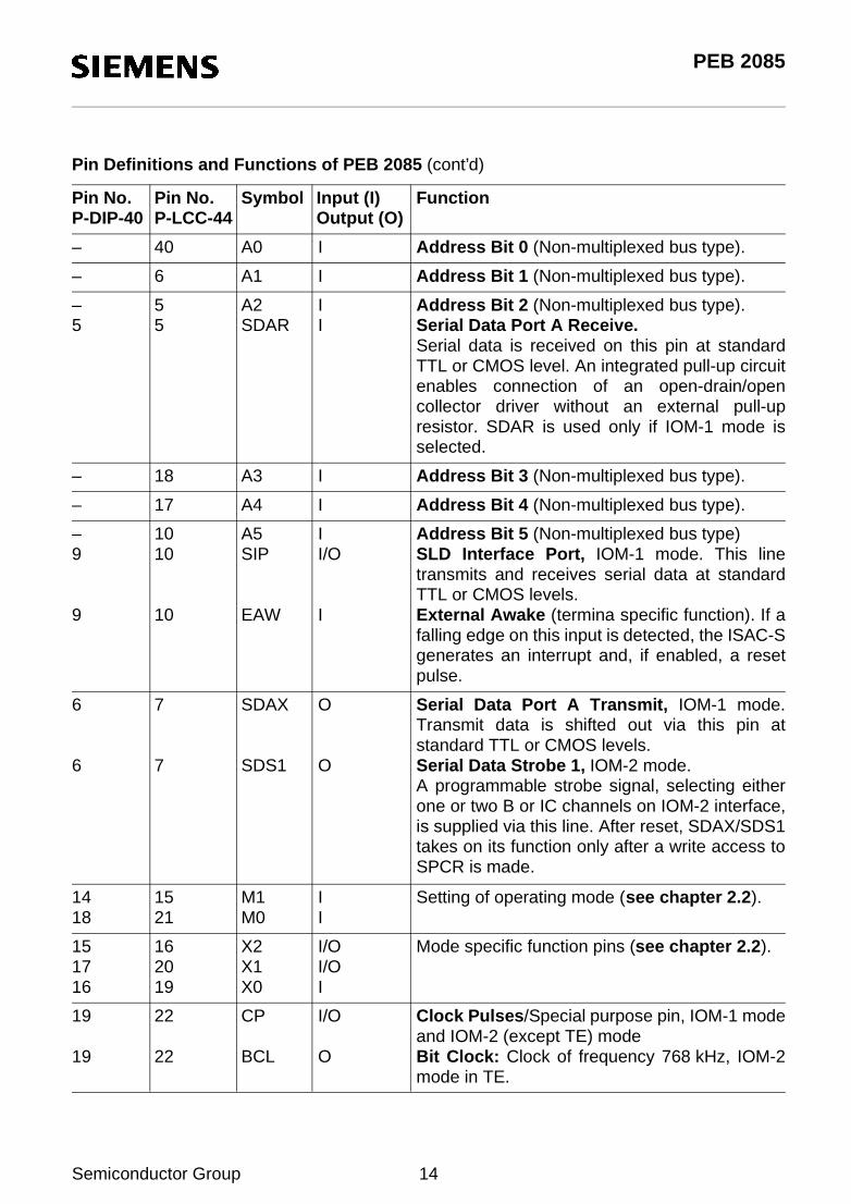
1.1.1 Pin Definitions and Functions of PEB 2085
Chip Select: A "Low" on this line selects the ISAC-S for a read/write operation.
34 37 CS
Multiplexed Bus Mode: Address/data bustransfers addresses from the µP system to theISAC-S and data between the µP system andthe ISAC-S.Non-Multiplexed Bus Mode: Data bus.Transfers data between the µP system and theISAC-S.
373839401234
414243441234
AD0/D0AD1/D1AD2/D2AD3/D3AD4/D4AD5/D5AD6/D6AD7/D7
FunctionSymbolPin No.P-DIP-40
Pin No.P-LCC-44
I
I/OI/OI/OI/OI/OI/OI/OI/O
Input (I)Output (O)Open Drain (OD)
Read/Write: When "High" identifies a valid µPaccess as a read operation. When "Low",identifies a valid µP access as a write operation(Motorola bus mode).
38 R/W I
Write: This signal indicates a write operation(Intel bus mode).
35 38 WR I
Data Strobe: The rising edge marks the end ofa valid read or write operation (Motorola busmode).
39 DS I
Read: This signal indicates a read operation(Intel bus mode).
36 39 RD I
Interrupt Request: The signal is activatedwhen the ISAC-S requests an interrupt. It is anopen drain output.
20 23 INT OD
Address Latch Enable: A high on this line indi-cates an address on the external address bus(multiplexed bus type only).ALE also selects the microprocessor interfacetype (multiplexed or non-multiplexed)P-LCC only.
33 36 ALE I
Semiconductor Group 12

PEB 2085
Pin Definitions and Functions of PEB 2085 (cont’d)
Serial Clock Port A, IOM-1 timing mode 0. A128-kHz data clock signal for serial port A (SSI).Frame Sync Delayed, IOM-1 timing mode 1. An8-kHz synchronization signal, delayed by 1/8 ofa frame, for IOM-1 is supplied. In this mode aminimal round-trip delay for B1 and B2 channelsis guaranteed.Serial Data Strobe 2, IOM-2 mode. Aprogrammable strobe signal, selecting eitherone or two B or IC channels on the IOM-2interface, is supplied via this line.After reset, SCA/FSD/SDS2 takes on its functiononly after a write access to SPCR is made.
7
7
7
8
8
8
SCA
FSD
SDS2
FunctionSymbolPin No.P-DIP-40
Pin No.P-LCC-44
O
O
O
Input (I)Output (O)
Reset: A "High" on this input forces the ISAC-Sinto reset state. The minimum pulse length isfour DCL clock periods or four ms. If the terminalspecific functions are enabled, the ISAC-S mayalso supply a reset signal.
8 9 I/ORST
Frame Sync 2:LT-S/LT-T/NT: input synchronization signalIOM-1 and IOM-2 modeTE: programmable strobe output, selectingeither B1 or B2 channel on the SSI interface.TE: Pull-up connection for IDP1, IOM-2 mode.
13 14 I/OFSC2
Frame Sync 1:LT-S/NT/LT-T: input synchronization signal,IOM-1 and IOM-2 modeTE: a programmable strobe output, selectingeither B1 or B2 channel on the SSI interface,IOM-1 modeTE: frame sync output, "High" during channel 0on the IOM-2 interface, IOM-2 mode.
12 13 I/OFSC1
Data Clock: Clock of frequency equal to twicethe data rate on the IOM interfaceLT-S/LT-T: clock input 512-kHz IOM-1 mode
4096-kHz IOM-2 modeTE: clock output 512-kHz IOM-1 mode
1536-kHz IOM-2 modeNT: clock input 512-kHz
11 12 I/ODCL
Semiconductor Group 13
PEB 2085
Pin Definitions and Functions of PEB 2085 (cont’d)
FunctionSymbolPin No.P-DIP-40
Pin No.P-LCC-44
Input (I)Output (O)
Address Bit 1 (Non-multiplexed bus type).– 6 IA1
Clock Pulses/Special purpose pin, IOM-1 modeand IOM-2 (except TE) modeBit Clock: Clock of frequency 768 kHz, IOM-2mode in TE.
19
19
22
22
I/O
O
CP
BCL
Address Bit 2 (Non-multiplexed bus type).Serial Data Port A Receive.Serial data is received on this pin at standardTTL or CMOS level. An integrated pull-up circuitenables connection of an open-drain/opencollector driver without an external pull-upresistor. SDAR is used only if IOM-1 mode isselected.
–5
55
II
A2SDAR
Address Bit 0 (Non-multiplexed bus type).– 40 IA0
Address Bit 4 (Non-multiplexed bus type).– 17 IA4
Address Bit 3 (Non-multiplexed bus type).– 18 IA3
Address Bit 5 (Non-multiplexed bus type)SLD Interface Port, IOM-1 mode. This linetransmits and receives serial data at standardTTL or CMOS levels.External Awake (termina specific function). If afalling edge on this input is detected, the ISAC-Sgenerates an interrupt and, if enabled, a resetpulse.
–9
9
1010
10
II/O
I
A5SIP
EAW
Serial Data Port A Transmit, IOM-1 mode.Transmit data is shifted out via this pin atstandard TTL or CMOS levels.Serial Data Strobe 1, IOM-2 mode.A programmable strobe signal, selecting eitherone or two B or IC channels on IOM-2 interface,is supplied via this line. After reset, SDAX/SDS1takes on its function only after a write access toSPCR is made.
6
6
7
7
O
O
SDAX
SDS1
Setting of operating mode (see chapter 2.2).1418
1521
II
M1M0
Mode specific function pins (see chapter 2.2).151716
162019
I/OI/OI
X2X1X0
Semiconductor Group 14

PEB 2085
Pin Definitions and Functions of PEB 2085 (cont’d)
FunctionSymbolPin No.P-DIP-40
Pin No.P-LCC-44
Input (I)Output (O)
Analog ground21 24 –VSSA
Connection for crystal or external clock inputConnection for external crystal. Leftunconnected if external clock is used.
2322
2625
IO
XTAL1XTAL2
IOM Data Port 0 (DD)IOM Data Port 1 (DU)IOM-1: IDP1: Open-drain with internal pull-
up resistorIDP0: Push-pull
IOM-2: Open drain without internal pull-up resistor or push-pull (ADF2:ODS)
3132
3435
I/OI/O
IDP0(DD)IDP1(DU)
Digital ground10 11 –VSSD
Power supply (5 V ± 5%)28 31 –VDD
S Bus Receiver InputS Bus Receiver Output (2.5 V reference)
2425
2728
IO
SR2SR1
Connection for external pre-filter for S Busreceiver, if used.
26 29 OUFI
S Bus Transmitter Output (positive)S Bus Transmitter Output (negative)
2930
3233
OO
SX1SX2
Semiconductor Group 15

PEB 2085
1.1.2 Logic Symbol of PEB 2085
Figure 1Logic Symbol of the ISAC®-S
IDP0
SDAR
VDD XTAL1 XTAL2
X0...2
M0...1
SR2
SX2
SX1
SR1
UFI
ITL02313
+ 5 V 0 V 0 V Reset
RSTSSAV VSSD
7.68 MHz ±100 ppm
IDP1
SDAX/SDS1
SIP/EAW
DCL
FSC1
CP/BCL
SCA/FSD/SDS2
FSC2
TR = 100
10 nF
*)
TR = 100 *)
AD0...7 (D0...7) (A0...5) CS
WR (R/W)
RD (DS) INT ALE
P
*) Terminating resistors only at the far ends of the connection
ModeSpecialFunctionPins
SSI
SLD
Clock FrameSynchronization
S/T
Ω
Ω
µ
RIOM
Semiconductor Group 16

PEB 2086
The PEB 2086 is an enhanced version of the PEB 2085. The PEB 2086 includes a symmetricalS/T-interface receiver and may use the M-bit of the S/T-interface frame for synchronizationpurposes.
The PEB 2086 is software compatible to the PEB 2085.
Type Ordering Code Package
PEB 2086H Q67100-H6307 P-MQFP-64-1 (SMD)
PEB 2086N Q67100-H6356 P-LCC-44-1 (SMD)
1.2 Features of PEB 2086
Enhanced version of the PEB 2085 with followingnew features:
Symmetrical S/T-interface receiver
B-channel mapping on SSI-interface
Demultiplexed microprocessor interface inIOM®-1 mode
Multiframe synchronization
P-MQFP-64-11
P-LCC-44-1
ISDN Subscriber Access Controller ISAC®-SCMOS IC
Semiconductor Group 17 10.94

PEB 2086
Pin Configuration(top view)
ITP03729
PEB 2086
64 17
N.C.
47
VSSD
N.C.
63
62
61
60
59
58
57
56
55
54
53
52
51
50
49N.
C.
1
N.C.
2
N.C.
3 4
MO
5
CP/B
CL
6
INT
7
N.C.
8 9
XTAL
2
10
XTAL
1
11 12
SR2
13
N.C.
14
SR1
15A3 N.C.A4 18 N.C.X2 19 N.C.
20 N.C.FSC2 21
FSC1 22 SX123 SX224 IDP0
SIP/EAW 25 IDP1A5 26 ALE
RST 27 CSSCA/FSD/SDS2 28 WR(R/W)
SDAX/SDS1 29 RD(DS)A1 30 A0A2 31 N.C.
SDAR 32 N.C.46
N.C.
45
N.C.
44
N.C.
43
AD7/
D7
42
AD6/
D6
41
AD5/
D5
40 39
AD3/
D3
38
AD2/
D2
37
AD1/
D1
36
AD0/
D0
35
N.C.
34
N.C.
33
N.C.
N.C.
16
48
SSA
V
DDV
X1
DCL
VDD
AD4/
A4
M1
P-MQFP-64
ITP03730
PEB 2086
AD2(
D2)
A0AD0(
D0)
AD1(
D1)
AD3(
D3)
AD4(
D4)
AD5(
D5)
AD6(
D6)
AD7(
D7)
SDAR
(A2)
SDAX/SDS1SCA/FSD/SDS2
RSTSIP/EAW/A5
DCLFSC1FSC2
M1X2A4
6 5 4 3 2 1 44 43 42 41 40
17
16
15
14
13
12
11
10
9
8
7 RD(DS)39
WR(R/W)38
CS37
ALE36
IDP135
IDP034
SX233
SX132
31
N.C.30
N.C.29
SR1
SR2
XTAL
1XT
AL2
INT
CP/B
CLM0
N.C.A3
2827262524232221201918
VSS
A
VSSD
VDD
A1
X1
P-LCC-44
Semiconductor Group 18

PEB 2086
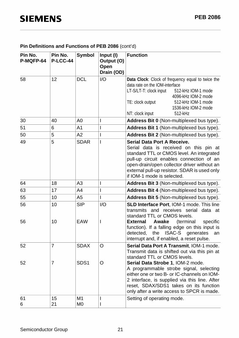
1.2.1 Pin Definitions and Functions of PEB 2086
Pin No.P-MQFP-64
Pin No.P-LCC-44
Symbol Input (I)Output (O)OpenDrain (OD)
Function
3738394041424344
414243441234
AD0/D0AD1/D1AD2/D2AD3/D3AD4/D4AD5/D5AD6/D6AD7/D7
I/OI/OI/OI/OI/OI/OI/OI/O
Multiplexed Bus Mode: Address/data bustransfers addresses from the µP system tothe ISAC-S and data between the µPsystem and the ISAC-S.Non-Multiplexed Bus Mode: Data bus.Transfers data between the µP system andthe ISAC-S.
27 37 CS I Chip Select: A “Low“ on this line selectsthe ISAC-S for a read/write operation.
28
28
38
38
R/W
WR
I
I
Read/Write: When “High“ identifies a validµP access as a read operation. When“Low“, identifies a valid µP access as awrite operation (Motorola bus mode).Write: This signal indicates a writeoperation (Intel bus mode).
29
29
39
39
DS
RD
I
I
Data Strobe: The rising edge marks theend of a valid read or write operation(Motorola bus mode).Read: This signal indicates a readoperation (Intel bus mode).
8 23 INT OD Interrupt Request: The signal is activatedwhen the ISAC-S requests an interrupt. It isan open drain output.
26 36 ALE I Address Latch Enable: A high on this lineindicates an address on the externaladdress bus (multiplexed bus type only).ALE also selects the microprocessorinterface type (multiplexed or non-multiplexed).
Semiconductor Group 19

PEB 2086
Pin Definitions and Functions of PEB 2086 (cont’d)
Pin No.P-MQFP-64
Pin No.P-LCC-44
Symbol Input (I)Output (O)OpenDrain (OD)
Function
53
53
53
8
8
8
SCA
FSD
SDS2
O
O
O
Serial Clock Port A, IOM-1 timing mode 0.A 128-kHz data clock signal for serial port A(SSI).Frame Sync Delayed, IOM-1 timingmode 1. An 8-kHz synchronization signal,delayed by 1/8 of a frame, for IOM-1 issupplied. In this mode a minimal round-tripdelay for B1- and B2-channels isguaranteed.Serial Data Strobe 2, IOM-2 mode. Aprogrammable strobe signal, selectingeither one or two B- or IC-channels on theIOM-2 interface, is supplied via this line.After reset, SCA/FSD/SDS2 takes on itsfunction only after a write access to SPCRis made.
54 9 RST I/O Reset: A “High“ on this input forces theISAC-S into reset state. The minimumpulse length is four DCL-clock periods orfour ms. If the terminal specific functionsare enabled, the ISAC-S may also supply areset signal.
59 13 FSC1 I/O Frame Sync 1:LT-S/NT/LT-T: input synchronizationsignal, IOM-1 and IOM-2 mode.TE: a programmable strobe output,selecting either B1- or B2-channel on theSSI-interface, IOM-1 mode.TE: frame sync output, “High“ duringchannel 0 on the IOM-2 interface, IOM-2mode.
60 14 FSC2 I/O Frame Sync 2:LT-S/LT-T/NT: input synchronizationsignal, IOM-1 and IOM-2 mode.TE: programmable strobe output, selectingeither B1- or B2-channel on the SSI-interface, IOM-1 mode.TE: Pull-up connection for IDP1, IOM-2mode.
Semiconductor Group 20
PEB 2086
58 12 DCL I/O Data Clock: Clock of frequency equal to twice thedata rate on the IOM-interfaceLT-S/LT-T: clock input 512-kHz IOM-1 mode
4096-kHz IOM-2 modeTE: clock output 512-kHz IOM-1 mode
1536-kHz IOM-2 modeNT: clock input 512-kHz
30 40 A0 I Address Bit 0 (Non-multiplexed bus type).
51 6 A1 I Address Bit 1 (Non-multiplexed bus type).
50 5 A2 I Address Bit 2 (Non-multiplexed bus type).
49 5 SDAR I Serial Data Port A Receive.Serial data is received on this pin atstandard TTL or CMOS level. An integratedpull-up circuit enables connection of anopen-drain/open collector driver without anexternal pull-up resistor. SDAR is used onlyif IOM-1 mode is selected.
64 18 A3 I Address Bit 3 (Non-multiplexed bus type).
63 17 A4 I Address Bit 4 (Non-multiplexed bus type).
55 10 A5 I Address Bit 5 (Non-multiplexed bus type).
56
56
10
10
SIP
EAW
I/O
I
SLD Interface Port, IOM-1 mode. This linetransmits and receives serial data atstandard TTL or CMOS levels.External Awake (terminal specificfunction). If a falling edge on this input isdetected, the ISAC-S generates aninterrupt and, if enabled, a reset pulse.
52
52
7
7
SDAX
SDS1
O
O
Serial Data Port A Transmit, IOM-1 mode.Transmit data is shifted out via this pin atstandard TTL or CMOS levels.Serial Data Strobe 1, IOM-2 mode.A programmable strobe signal, selectingeither one or two B- or IC-channels on IOM-2 interface, is supplied via this line. Afterreset, SDAX/SDS1 takes on its functiononly after a write access to SPCR is made.
616
1521
M1M0
II
Setting of operating mode.
Pin Definitions and Functions of PEB 2086 (cont’d)
Pin No.P-MQFP-64
Pin No.P-LCC-44
Symbol Input (I)Output (O)OpenDrain (OD)
Function
Semiconductor Group 21

PEB 2086
625
1620
X2X1
I/OI/O
Mode specific function pins.
7
7
22
22
CP
BCL
I/O
O
Clock Pulses/Special purpose pin, IOM-1mode and IOM-2 (except TE) mode.Bit Clock: Clock of frequency 768 kHz,IOM-2 mode in TE.
57 11 VSSD – Digital ground
10 24 VSSA – Analog ground
13, 21 31 VDD – Power supply (5 V ± 5 %)
12
11
26
25
XTAL1
XTAL2
I
O
Connection for crystal or externalclock input.Connection for external crystal.Left unconnected if external clock is used.
1416
2728
SR2SR1
II
S-Bus Receiver InputS-Bus Receiver Input
2223
3233
SX1SX2
OO
S-Bus Transmitter Output (positive)S-Bus Transmitter Output (negative)
2425
3435
IDP0(DD)IDP1(DU)
I/OI/O
IOM-Data Port 0 (DD)IOM-Data Port 1 (DU)IOM-1: IDP1:Open-drain with internal pull-
up resistorIDP0: Push-pull
IOM-2: Open drain without internal pull-upresistor or push-pull (ADF2:ODS)
Pin Definitions and Functions of PEB 2086 (cont’d)
Pin No.P-MQFP-64
Pin No.P-LCC-44
Symbol Input (I)Output (O)OpenDrain (OD)
Function
Semiconductor Group 22
PEB 2086
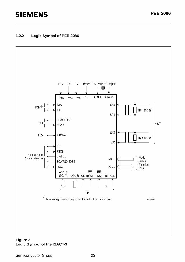
1.2.2 Logic Symbol of PEB 2086
Figure 2Logic Symbol of the ISAC®-S
IDP0
SDAR
VDD XTAL1 XTAL2
X1...2
M0...1
SR2
SX2
SX1
SR1
ITL03792
+ 5 V 0 V 0 V Reset
RSTSSAV VSSD
7.68 MHz ± 100 ppm
IDP1
SDAX/SDS1
SIP/EAW
DCL
FSC1
CP/BCL
SCA/FSD/SDS2
FSC2
TR = 100 *)
TR = 100 *)
AD0...7 (D0...7) (A0...5) CS
WR (R/W)
RD (DS) INT ALE
P
*) Terminating resistors only at the far ends of the connection
ModeSpecialFunctionPins
SSI
SLD
Clock FrameSynchronization
S/T
µ
Ω
Ω
RIOM
Semiconductor Group 23

Features
1.3 Functional Block Diagram
Figure 3Block Diagram of the ISAC®-S
ITB00843
FIFO
D-ChannelHandling
B-Channel
SwitchingInterface
Control
BufferISDNBasicAccess
Layer-1Functions
P Interfaceµ
SSI
SLD
SLD
SSI
P
S
RIOM
RIOM
µ
Semiconductor Group 24

Features
1.4 System Integration
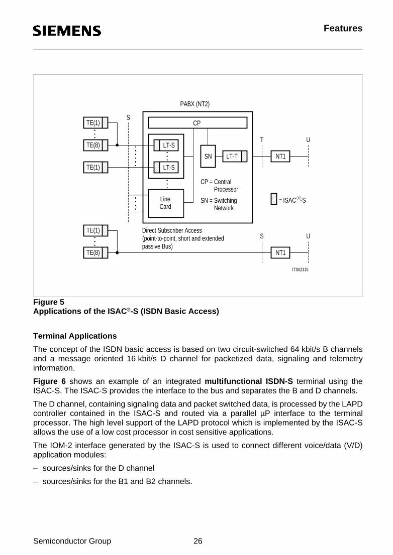
1.4.1 ISDN Applications
The reference model for the ISDN basic access according to CCITT I series recommendationsconsists of
– an exchange and trunk line termination in the central office (ET, LT)
– a remote network termination in the user area (NT)
– a two-wire loop (U interface) between NT and LT
– a four-wire link (S interface) which connects subscriber terminals and the NT in the userarea as depicted in figure 4.
Figure 4ISDN Basic Subscriber Access Architecture
The NT equipment serves as a converter between the U interface at the exchange and theS interface at the user premises. The NT may consist of either an NT1 only or an NT1 togetherwith an NT2 connected via the T interface which is physically identical to the S interface. TheNT1 is a direct transformation between layer 1 of S and layer 1 of U. NT2 may include higherlevel functions like multiplexing and switching as in a PABX.
The ISAC-S is designed for the user area of the ISDN basic access, especially for subscriberterminal equipment and for exchange equipment with S interfaces. Figure 5 illustrates thegeneral applications of the ISAC-S.
ITS02314
NT
NT1
NT2 NT1T
TE
TE
LT ET
S U
ISDN User Area ISDN Central Office
Semiconductor Group 25
Features
Figure 5Applications of the ISAC®-S (ISDN Basic Access)
Terminal Applications
The concept of the ISDN basic access is based on two circuit-switched 64 kbit/s B channelsand a message oriented 16 kbit/s D channel for packetized data, signaling and telemetryinformation.
Figure 6 shows an example of an integrated multifunctional ISDN-S terminal using theISAC-S. The ISAC-S provides the interface to the bus and separates the B and D channels.
The D channel, containing signaling data and packet switched data, is processed by the LAPDcontroller contained in the ISAC-S and routed via a parallel µP interface to the terminalprocessor. The high level support of the LAPD protocol which is implemented by the ISAC-Sallows the use of a low cost processor in cost sensitive applications.
The IOM-2 interface generated by the ISAC-S is used to connect different voice/data (V/D)application modules:
– sources/sinks for the D channel
– sources/sinks for the B1 and B2 channels.
ITS02315
LT-S
LT-S
LT-TSN
CP
LineCard
TE(8)
TE(1)
TE(1)S
CP
SN
=
= SwitchingNetwork
CentralProcessor
PABX (NT2)
NT1
T U
=
TE(1)
TE(8)
US
NT1
Direct Subscriber Access (point-to-point, short and extendedpassive Bus)
RISAC -S
Semiconductor Group 26

Features
Figure 6Example of an ISDN®-S Voice/Data Terminal
Up to eight D channel components (ICC: ISDN Communication Controller PEB 2070) may beconnected to the D and C/I (Command/Indication) channels (TIC bus). The ISAC-S and ICChandle contention autonomously.
Data transfers between the ISAC-S and the voice/data modules are done with the help of theIOM MONITOR channel protocol. Each V/D module can be accessed by an individual address.The same protocol enables the control of IOM terminal modules and the allocation ofintercommunication channels inside the terminal. Two intercommunication channels IC1 andIC2 allow a 2 × 64 kbit/s transfer rate between voice/data modules.
In the example above (figure 6), one ICC is used for data packets in the D channel. A voiceprocessor is connected to a programmable digital signal processing codec filter via IC1 and adata encryption module to a data device via IC2. B1 is used for voice communication, B2 fordata communication.
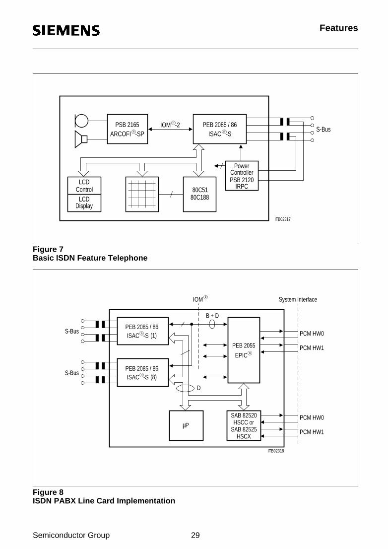
The ISAC-S ensures full upward compatibility with IOM-1 devices. It provides the additionalstrobe, clock and data lines for connecting standard combos or data devices via IOM, or serialSLD and SSI interfaces. The strobe signals and the switching of B channels is programmable.Figure 7 shows the implementation of a basic ISDN feature telephone using the ISAC-S andthe Audio Ringing Codec Filter featuring speakerphone (ARCOFI®-SP: PSB 2165).
PEB 2085 ICCPEB 2070
SpeechProcessing DSP-COFI Data
EncryptionHSCX
SAB 8252X
C
ITD02316Data Module Speech Modules Data Modules
C/I B1 IC1 B2 IC2
µ
PEB 2086
D,
RIOM -2
RISAC -S
Semiconductor Group 27

Features
Line Card Applications
An example of the use of the ISAC-S on an ISDN PABX line card (decentralized architecture)is shown in figure 8.
The ISAC-S is connected to an Extended PCM Interface Controller (EPIC PEB 2055) via anIOM interface.
This interface carries the control and data for up to eight subscribers using time divisionmultiplexing. The ISAC-S’s are connected in parallel on the IOM (IDP0 output; IDP1, DCL,FSC1/2 as inputs), one ISAC-S per subscriber.
The EPIC performs dynamic B- and D-channel assignment on the PCM highways. Since thiscomponent supports four IOM interfaces, up to 32 subscribers may be accommodated.
1.4.2 Microprocessor Environment
The ISAC-S is especially suitable for cost-sensitive applications with single-chipmicrocontrollers (e.g. 8048, 8031, 8051). However, due to its programmable micro- processorinterface and non-critical bus timing, it fits perfectly into almost any 8-bit microprocessorsystem environment. The microcontroller interface can be selected to be either of the Motorolatype (with control signals CS, R/W, DS) of the Siemens/Intel non-multiplexed bus type (withcontrol signals CS, WR, RD) or of the Siemens/Intel multiplexed address/data bus type (CS,WR, RD, ALE).
An example how to connect the ISAC-S to a Siemens/Intel microcontroller is shown in figure 9.
Semiconductor Group 28
Features
Figure 7Basic ISDN Feature Telephone
Figure 8ISDN PABX Line Card Implementation
ITB02317
PEB 2085 / 86PSB 2165
PowerControllerPSB 2120
IRPC
S-Bus
80C5180C188
LCDControl
LCDDisplay
RARCOFI -SP
RIOM -2ISAC -SR
ITB02318
PEB 2085 / 86
SAB 82520HSCC or
SAB 82525HSCX
S-Bus (1)
(8)S-Bus
P
B + D
D
PEB 2055
System Interface
PCM HW1
PCM HW0
PCM HW0
PCM HW1µ
RIOM
REPIC
RISAC -S
PEB 2085 / 86ISAC R -S
Semiconductor Group 29

Features
Figure 9Connecting the ISAC®-S to Siemens/Intel Microcontroller
INT(INTX)
RD
WR
ALE
(PSCX)
AD7...AD0
INT
ALE
CS
AD7...AD0AD0 - AD7
LatchA8-A
15
Memory
Common Bus A15-A0, D7-D0
ITS02319
SLD
PEB 2085 (80C188)80C51
A15...A8
SX2
SR1
SX1
SR2
SSI
S0
+ 5 V
ALE
WR
RD
WR
RD
PEB 2086
RIOM -2
RISAC -S
Semiconductor Group 30

Functional Description
2 Functional Description
2.1 General Functions and Device Architecture
The functional block diagram of the ISAC-S is shown in figure 10.
The left-hand side of the diagram contains the layer-1 functions, according to CCITT I seriesrecommendations:
– S-bus transmitter and receiver
– timing recovery and synchronization by means of digital PLL circuitry
– activation/deactivation
– access to S and Q channels
– handling of D channel
– test loops
– send single/continuous AMI pulses (diagnostics).
Figure 10Architecture of the ISAC®-S
ITB00850
LAPDControllerStatusCommandRegisterFIFOController
HDLCReceiver
HDLCTransmitter
X-FIFOR-FIFO
Interface
BufferAMI
BIN
D-CHAccess
Control
DPLL
Timing
P-Interfaceµ
BINAMI
Buffer
IDP1 IDP0
XTAL1
XTAL2
SR1
SR2
SX2
SX1
VSSA
DDV
DCLCP/BCL FSC1 SCA/FSD/SDS2
AD0-AD7/A0-A5&D0-D7
Control INT
RST
V SSD
UFI*
*
M1 M0
FSC2X0, X1, X2*
* Only PEB 2085
SSI Port
SLD PortSIP/EAW
SDAX/
SDAR
SDS1
RIOM
Semiconductor Group 31
Functional Description
The right-hand side consists of:
– the serial interface logic for the IOM and the SLD and SSI interfaces, with B-channelswitching capabilities
– the logic necessary to handle the D-channel messages (layer 2).
The latter consists of an HDLC receiver and an HDLC transmitter together with 64-byte deepFIFO's for efficient transfer of the messages to/from the user's CPU.In a special HDLC controller operating mode, the auto mode, the ISAC-S processes protocolhandshakes (I- and S-frames) of the LAPD (Link Access Procedure on the D channel)autonomously.Control and monitor functions as well as data transfers between the user's CPU and the D andB channels are performed by the 8-bit parallel µP interface logic.The IOM interface allows interaction between layer-1 and layer-2 functions. It implements D-channel collision resolution for connecting other layer-2 devices to the IOM interface (TIC bus),and the C/I and MONITOR channel protocols (IOM-1/IOM-2) to control peripheral devices.The timing unit is responsible for the system clock and frame synchronization.
2.2 Interface and Operating Modes
The ISAC-S is configurable for the following applications:
– ISDN terminals → TE mode
– ISDN subscriber line termination → LT-S mode
– ISDN network termination → NT mode
– ISDN trunk line termination → LT-T mode(PABX connection to Central Office)
Configuration is performed by pin-strapping (pins M1, M0), yielding different meanings to themultifunctional pins (X0 (PEB 2085 only), X1, X2) as well as the clock and framing signal pins(DCL, FSC1, FSC2, CP) see table 1 and 2.Two basic modes are distinguished, according to whether the ISAC-S is programmed tooperate with the IOM-1 or with the IOM-2 interface. This programming is performed via bit IMSin the ADF2 register.
2.2.1 IOM®-1 Interface Mode (ADF2:IMS=0)
In this mode the IOM-1 interface is primarily used to interconnect the layer-1 and layer-2 partsinside the ISAC-S. B-channel interfacing is performed via the auxiliary serial SSI and SLDinterfaces.The external availability of the IOM interface ports (IDP0, 1) can be used for TIC busapplications (several layer-2 devices occupying the same D and Command/Indicate channelconnected to one layer-1 device).The Timing Mode (SPCR:SPM) defines the operating mode of the SLD interface (master/slave) and the phase relationship between the SLD and IOM interface (see chapter 2.3.1).The operating modes are shown in table 1.
Semiconductor Group 32

Functional Description
Table 1Operating Modes and Functions of Mode Specific Pins of the ISAC®-S PEB 2085/86 in the IOM®-1 Mode
*) synchronized to the S/T interface i:input o:output i:o : input to be fixed at "0"**) PEB 2086 only
ECHO/M The value of the M-bit is output, multiplexed with the value of the Echo-bits on theIOM-interface.Reproduces the E-bits received from the S interface synchronously to IOM frame"D"-bits (bit positions 24 and 25 of the IOM frame). All other bit positions, except theM-bit are binary "1".
SFS S-Frame Start. A 4 kHz synchronization signal is used to sample the value of the M-bit and to synchronize the start of the S-frame. Note that the M-bit functions are onlyavailable on the PEB 2086.
SSYNC Superframe/Multiframe Synchronization. This input is used to reset the multiframecounter. It is sampled by SFS.
SCZ Send continuous binary zeros (96 kHz)
SSZ Send single binary zeros (2 kHz)
Pin No.P-DIP-40(PEB 2085 only)
14 18 11 12 13 19 15 17 16
Pin No.P-LCC-44
15 21 12 13 14 22 16 20 19
Pin No.P-MQFP-64(PEB 2086 only)
61 6 58 59 60 7 62 5 –
Application M1 M0 DCL FSC1 FSC2 CP X2 X1 X0
TE 0 0 o:512 kHz* o:8 kHz* o:8 kHz* o:1536 kHz* o:ECHO/M** o:3840 kHz i:CON
LT-T 0 1 i:512 kHz i:8 kHz i:8 kHz o:512 kHz* i:o i:o i:CON
LT-S 1 0 i:512 kHz i:8 kHz i:8 kHz i:o/i:SFS** i:o/i:SSYNC o:7680 kHz i:o
NT 1 1 i:512 kHz i:8 kHz i:8 kHz i:SCZ/i:4 kHz**
i:SSZ i:o –
Semiconductor Group 33

Functional Description
CON Connected to the S bus. Only available on PEB 2085.
CON = 0: Disconnected from the S bus; an activation of the S/T line initiated bythe TE/LT-T is not possible: Info 1 cannot be transmitted. An activationinitiated by the network (reception of Info2/Info4) is still possible.
CON = 1: Connected to the S bus; normal operation, transmission of Info 1(upon an ARU command) is possible.
– not used
X0 Mode Specific Pin (PEB 2086)
The X0 pin of the PEB 2085 ISAC-S which was intended for the CON-input (Connected to theS-Bus) has been eliminated on PEB 2086. As a result, the C/I response DIS (Disconnect) willnot be generated.
Semiconductor Group 34

Functional Description
The different operating modes in relation to the timing recovery are illustrated in figure 11.
Figure 11Operating Modes of the ISAC®-S (IOM®-1)
ITS00844NT Mode
PEB 2091
IDP0
IDP1
DCL
PEB 2085/86
FSC1FSC2
S U
CLOCK MASTERCLOCK SLAVE
LT-T Mode, Timing Mode 1System Int.
T
CLOCK SLAVE CLOCK MASTER
DCLFSC2 FSC1
PEB 2085/86
System Int.S
TE Mode, Timing Mode 0
PEB 2085/86
S
CLOCK MASTER
SIP
SCLK
SIP
FSD
LT-S Mode, Timing Mode 1
PEB 2050/52/55
SYP CLK
SIP
DCLFSC1
SDAXSDARTYPE 2
TYPE 1
FSC2SCASSI
512 kbit/s
512 kHz8 kHz
128 kbit/s
128 kbit/s
kHz8kHz128
512 kbit/s
512 kHz
kHz84096 kHz
FSD
SIP
PEB 2085/86
FSC1 FSC2DCLCLK SYP
PEB 2050/52/55SCLK
SIP
CLOCK MASTER CLOCK SLAVE
kHz40968 kHz
kHz512
kbit/s512
kHz8
512 kHz
256 kbit/s
256 kbit/s
SLD
Semiconductor Group 35

Functional Description
2.2.2 IOM®-2 Interface Mode (ADF2:IMS=1)
In this mode the IOM interface has the enhanced functionality of IOM-2. B-channel interfacingis performed directly via the IOM-2 interface and the auxiliary serial SSI and SLD interfacesare not longer available (as in IOM-1 mode), since they are functionally replaced by the generalpurpose IOM-2 interface.
The Serial Port Timing Mode (SPCR:SPM) defines the operating mode of the IOM-2 interfacei.e. either the terminal mode frame structure (3 channels) or the non-terminal frame structure(8 channels) can be selected (see chapter 2.4.1).
The serial port timing mode must be set in accordance to the operating mode, i.e. the TE moderequires the terminal timing mode and LT-S/LT-T modes require non-terminal timing-mode.
In NT mode the IOM frame structure is identical to that of the IOM-1 case (1 channel) and thenon-terminal timing mode must be selected.
The operating modes are shown in table 2.
Table 2Operating Modes and Functions of Mode Specific Pins of the ISAC®-S PEB 2085/86 in IOM®-2 Mode
*) synchronized to the S/T interface i:input o:output i:o : input to be fixed at "0"
ECHO/M The value of the M-bit is output, multiplexed with the value of the Echo-bits on theIOM-interface.Reproduces the E-bits received from the S interface synchronously to IOM frame"D"-bits (bit positions 24 and 25 of the IOM frame). All other bit positions, except theM-bit are binary "1".
Pin No.P-DIP-40(PEB 2085 only)
14 18 11 12 13 19 15 17 16
Pin No.P-LCC-44
15 21 12 13 14 22 16 20 19
Pin No.P-MQFP-64(PEB 2086 only)
61 6 58 59 60 7 62 5 –
Application M1 M0 DCL FSC1 FSC2 CP X2 X1 X0
TE 0 0 o:1536 kHz* o:8 kHz* o:PU1 o:768 kHz* o:ECHO/M** o:PU0 i:CON
LT-T 0 1 i:4096 kHz i:8 kHz i:8 kHz o:512 kHz* i:o i:o i:CON
LT-S 1 0 i:4096 kHz i:8 kHz i:8 kHz i:o i:o o:7680 kHz i:o
NT 1 1 i:512 kHz i:8 kHz i:8 kHz i:SCZ i:SSZ i:o –
Semiconductor Group 36

Functional Description
SCZ Send continuous binary zeros (96 kHz)
SSZ Send single binary zeros (2 kHz)
CON Connected to the S bus.
CON = 0: Disconnected from S bus; an activation of the S/T line initiated by the TE/LT-T is not possible: Info 1 cannot be transmitted. An activation initiated by the network (reception of Info2/Info4) is stillpossible.
CON = 1: Connected to the S bus; normal operation, transmission of Info 1 (upon an ARU command) is possible.
PU0 Pull-up pin for IDP0 (power saving option in TE mode, see chapter 2.4.2)PU1 Pull-up pin for IDP1 (power saving option in TE mode, see chapter 2.4.2)
– not used
X0 Mode Specific Pin (PEB 2086)
The X0 pin of the PEB 2085 ISAC-S which was intended for the CON-input (Connected to theS-Bus) has been eliminated on PEB 2086. As a result, the C/I response DIS (Disconnect) willnot be generated.
Semiconductor Group 37

Functional Description
The different operating modes in relation to the timing recovery are illustrated in figure 12.
Figure 12aOperating Modes of ISAC®-S (IOM®-2)
768
7688
81536
CLOCK MASTER
S
IDP1
IDP0PEB 2085/86
DCL FSC1 BCL SDS1/2V/D Module
TE Mode, Terminal Timing Mode
S
LT-S Mode, Non-Terminal Timing Mode
System Int.
PEB 2055PEB 2085/86
FSC1FSC2
IDP0
IDP1
DCL
CLOCK MASTERCLOCK SLAVE
ITS03426
kHzkHz
kHzkHz
kbit/s
kbit/s768
8 kHz
kHz4096
2048 kbit/s
2048 kbit/s
(DD)
(DU)
Semiconductor Group 38

Semiconductor Group 39
Functional Description
Figure 12bOperating Modes of ISAC®-S (IOM®-2)
ITS00851
NT Mode
PEB 2091
IDP0
IDP1
DCL
PEB 2085/86
FSC1FSC2
S U
CLOCK MASTERCLOCK SLAVE
LT-T Mode, Non-Terminal Timing Mode
System Int. T
PEB 2055 PEB 2085/86
FSC1 FSC2
IDP0
IDP1
DCL
CLOCK MASTER
2048 kbit/s
2048 kbit/s
4096 kHz
8 kHz
256 kbit/s
kHz8
512 kHz
256 kbit/s
CLOCK MASTER

Functional Description
2.3 IOM®-1 Mode Functions
2.3.1 IOM®-1 Frame Structure / Timing Modes
This interface consists of one data line per direction (IOM Data Ports 0 and 1:IDP0, 1). Threeadditional signals define the data clock (DCL) and the frame synchronization (FSC1/2) at thisinterface. The data clock has a frequency of 512 kHz (twice the data rate) and the frame syncclock has a repetition rate of 8 kHz.
Via this interface four octets are transmitted per 125 µs frame (figure 13). The first two octetsconstitute the two 64 kbit/s B channels. In the ISAC-S the MONITOR channel (third octet)serves:
– for arbitration of the access to the IOM-TIC bus on IDP1 in case several layer-2 componentsare connected together (see chapter 2.3.9).
– to indicate the status on the S bus D channel (IDP0, bit 3 of the monitor octet), "stop/go"(see chapter 2.5.7).
– for the exchange of data using the IOM-1 MONITOR channel protocol which involves the Ebit as data validation bit (see chapter 2.3.7).
Two bits in the fourth octet are used for the 16 kbit/s D channel. The controlling and monitoringof layer-1 functions (activation/deactivation of the S interface...) is done via the Command/Indication bits. The T bit is not used in ISAC-S IOM-1 applications.
Figure 13IOM®-1 Frame Structure
IOM®-1 Timing
In TE mode the IOM timing is internally generated by DPLL circuitry from the S interface andDCL and FSC 1/2 are outputs.
In LT-S, NT and LT-T modes the clock and frame synchronization signals are inputs.
The IOM interface can be operated either in timing mode 0 or in timing mode 1, selected bySPM bit in SPCR register.
ITD00852
B1 B2 MONITOR D T EΙC /
TIC-Bus
125 µs
Semiconductor Group 40

Functional Description
Timing Mode 0 (SPM = 0)
In timing mode 0 the SLD operates in master mode and the SSI (Serial Port A) is operational;pin SCA/FSD delivers a 128-kHz clock (SCA). The IOM, SLD and SSI interface frame begin isat the same point in time i.e. at the rising edge of FSC1,2 (ADF1:FC2,1=0).
In TE mode, it is mandatory to program timing mode 0. The polarity of the symmetrical 8-kHzoutput signals FSC1 and FSC2 can be independently selected via ADF1:FC2, 1.
In LT-T and LT-S modes, timing mode 0 may be programmed if the SLD master mode and/or the SSI interface is required.
In these cases FSC1 and FSC2 (inputs) should both be connected to the same 8-kHz framesync signal (see figure 14).
Figure 14IOM®-1 Interface Signals/Timing Mode 0
ITS00853
IDP1IDP0DCLFSC1/2
TE ModeTiming Mode 0
CompatibleCommunicationsController
LT-T, LT-S ModeTiming Mode 0
CompatibleController
IDP1IDP0DCL
FSC1FSC2
FSC (Syst.)
CLK (Syst.)
SLD/SSI Frames
Frame
FSC1/2
(ADF1 : FC2,1 = 00)
RIOM -2
RIOM
RISAC -S
RIOM -2
IOM R
ISAC -SR
IOM R
Semiconductor Group 41

Functional Description
Timing Mode 1 (SPM = 1)
Timing mode 1 (SPM = 1) is only meaningful in exchange applications (LT-S, LT-T) when theSLD is used.
In timing mode 1 the SLD operates in slave mode and the SSI (Serial Port A) is no longeravailable.
The IOM is synchronized by a frame signal FSD delayed in time respect to the frame syncpulse input via FSC1. This reduces the B-channel round-trip delay time when the SLD is used(figure 15).
For correct operation in timing mode 1, the output FSD should be connected to the FSC2 input (see figures 11 and 15).
Figure 15IOM®-1 Interface Signals/Timing Mode 1
IDP1IDP0DCL
FSC2FSDFSC1
SIP
CompatibleController
LT-T, LT-S ModeTiming Mode 1
SLD
SLD (Syst.)FSC (Syst.)
CLK (Syst.)
IDP1: = 256 kbit/sIDP0: = 256 kbit/s
1/8 Frame Period
FSC1 (System)
FSC2 (IOM ITS02328
DCL: = 512 kbit/sFSC: = 8 kHz
RIOM
IOM RRISAC -S
R )
Semiconductor Group 42

Functional Description
2.3.2 IOM®-1 Interface Connections
In IOM-1 interface mode
– pin IDP0 carries B channel, MONITOR, D and C/I data from layer-1 to layer-2
– pin IDP1 carries B channel, MONITOR, D and C/I data from layer-2 to layer-1.
IDP1 is an open drain output with an integrated pull up circuitry. The B channels can be setinactive (FFH) by setting the B channel connect bits C1C1-0 and C2C1-0 in the SPCR registerto 0 (SLD loop), which is the state after a hardware reset.
The MONITOR channel is inactive (FFH) if no MONITOR channel transfer is programmed andthe TIC bus (i.e. the fourth octet of IOM frame: D and C/I channels) is not accessed.
Figure 16IOM®-1 Data Ports 0, 1 (IOM®-1)
P
IDP1
Layer-2e.g. ICC(PEB 2070)
IDP0IDP0
FunctionsLayer-2
IDP1
P
(Open Drain)
IDP0IDP1
IDP0IDP1
Layer-1Functions
S/T InterfaceVDD
C/I Channel)theControllers can have access toOptional: Up to 7 Layer 2
ITS02329
µ µ
RISAC -S
RIOM -1 TIC Bus
RIOM -1 TIC Bus (D and
Semiconductor Group 43

Functional Description
2.3.3 SLD Interface
The standard SLD interface is a three-wire interface with a 512-kHz clock (DCL), an 8-kHzframe direction signal (TE mode: FSC1/2 output; LT-S/LT-T modes: FSC1 sync input), and aserial ping-pong data lead (SIP) with an effective full duplex data rate of 256 kbit/s.
The frame is composed of four octets per direction. Octets 1 and 2 contain the two B channels,octet 3 is a feature control byte, and octet 4 is a signaling byte (figure 17).
The SLD interface can be used in:
– Terminal applications (TE) as a full duplex time-multiplexed (ping-pong) connection toB-channel sources/destinations.
CODEC filters, such as the SICOFI® (PEB 2060) or the ARCOFI (PSB 2160) as well as otherSLD compatible voice/data modules may be connected directly to the ISAC-S as depictedin figure 16. In TE applications timing mode 0 (SPCR:SPM=0) has to be programmed,hence SLD operates in master mode. Moreover, terminal specific functions have to bedeselected (STCR:TSF=0).
The µC system has access to B-channel data, the feature control byte and the signaling bytevia the ISAC-S registers:
– C1R (35H), C2R (36H) → B1/B2
– SFCR and SFCW (34H) → FC
– SSCR and SSCX (33H) → SIG
The µP access to C1R, C2R and SFCR/SFCW must be synchronized to the serialtransmission by means of the Synchronous Transfer Interrupt (STCR) and the BVS-bit(STAR) (see chapter 2.3.6).
Figure 17Connection of B-Channel Sources/Destinations to the ISAC®-S via SLD in Timing Mode 0
ITS00858
512 kbit/s
8 kHz
512SLD CompatibleVoice/Data
Module
B-Channel Source/Destination
SIP
DCL
FSC1/2TE Mode
Timing Mode 0
ISDN Sunscriber AccessSLD
Timing Mode 0
SSLD INSLD OUT
SIGFCB2B1SIP B1 B2 FC SIG
FSC1/2
kHzRISAC -S
Semiconductor Group 44
Functional Description
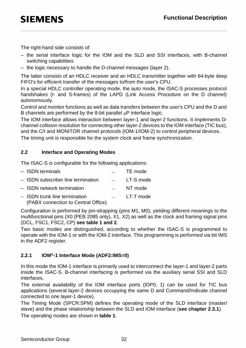
– Digital exchange applications (LT-S/LT-T) as a full duplex time-multiplexed connection toconvey the B channels between the S/T interface and a Peripheral Board Controller (e.g.PBC PEB 2050 or PIC PEB 2052), which performs time-slot assignment on the PCMhighways, forming a system interface to a switching network (figure 18).
Timing mode 1 (SPCR:SPM=1) has to be programmed, hence SLD operates in slave mode.
Figure 18Connection of the ISAC®-S as B-Channel Source/Destination to a Peripheral Board Controller via SLD, in Timing Mode 1
The µC system has access to B-channel data via the ISAC-S registers:
– C1R (35H), C2R (36H) → B1/B2
The µP access to C1R and C2R must be synchronized to the serial transmission by means ofSynchronous Transfer Interrupt (STCR) and the BVS bit (STAR) (see chapter 2.3.6).
ITS00859
512 kbit/s
8 kHz
512
SIPX
SCL
SYP
PBC
SLDS
SLD INSLD OUT
SIGFCB2B1SIP B1 B2 FC SIG
FSC1
kHz
FSD
1/8 Frame Period
TimingMode 1
SIP
DCL
1FSC
2FSC FSD
LT-S/LT-T CLK
PCM Highway
System InterfaceRISAC -S
Semiconductor Group 45
Functional Description
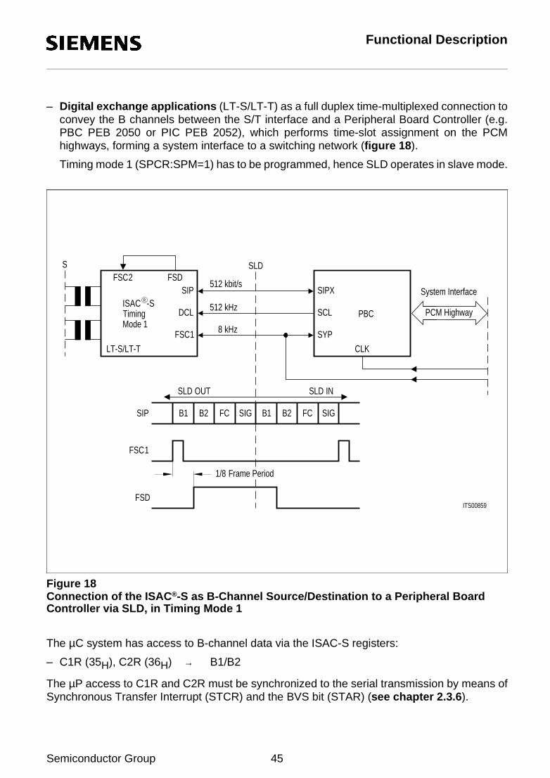
2.3.4 SSI (Serial Port A)
The SSI (Serial Synchronous Interface) is available only in timing mode 0 (SPCR:SPM=0).
The serial port SSI serves as a full duplex connection to B-channel sources/destinations interminal equipment with a data rate of 128 kbit/s.
Both channels B1 and B2 can be switched independently of one another to the IOM-1 interfaceand thus to the S/T interface (SPCR:CxC1, CxC0).
In case of the PEB 2086, the B1- and B2-channels are handled as one 128-kbit/s channel. Thedata transfer between SSI an IOM is shown in figure 22d.
The SSI consists of one data line in each direction (SDAX and SDAR), an 8-kHz strobe output(FSC1 and/or FSC2) and the 128-kHz clock output (SCA).
Figure 19Connection of the B-Channel Sources/Destinations to the ISAC®-S via SSI
This serial interface allows the connection of Voice/Data modules, such as serial synchronoustransceiver devices (USART’s, ICC PEB 2070, HSCX SAB 82525, ITAC®, PSB 2110...) andvarious CODEC filters directly to the ISAC-S, as illustrated in figure 19.
By programming the ADF1 register it is possible to independently set the strobe signal FSC1/2 polarities so that either B1 or B2 is selected by the V/D module.
The µC system has access to B-channel data via the ISAC-S registers BxCR and CxR.
The µC access must be synchronized to the serial transmission by means of the SynchronousTransfer Interrupt STCR (see chapter 4).
ITS00857
128 kbit/s
8 kHz
128Voice/Data
Module
B-Channel Source/Destination
SDAR
SDAX
FSC1/2TE Mode
Timing Mode 0
ISDN Sunscriber AccessSSI
S
B2SDAR, B1
FSC1/2
kHz
128 kbit/s
SCA
X
*)
)* Default Polarity(ADF1 Register)
RISAC -S
Semiconductor Group 46

Functional Description
2.3.5 B-Channel Switching
The ISAC-S contains two serial interfaces, SLD and SSI, which can serve as interfaces to Bchannel sources/destinations. Both channels B1 and B2 can be switched independently of oneanother to the IOM interface and to the four-wire S/T interface (figure 20).
The following possibilities are provided:
– Switching from/to SSI
– Switching from/to SLD
– IOM looping
– SLD looping.
The microcontroller can select the B-channel switching in the SPCR register. In figure 21 allpossible selections of the B-channel routes and access to B-channel data via themicroprocessor interface are illustrated. This access from the microcontroller is possible bywriting or reading the C1R/C2R register or reading the B1CR/B2CR register (seeSynchronous Transfer, paragraph 2.3.6).
Figure 20Principle of B-Channel Switching
P-Interfaceµ
Registers : C1R / C2RB1CR / B2CRSPCR
SSI
SLD
SLD
SSI
Interface
ITB00862
B-ChannelSources /Destinations
AccessBasicISDN
FunctionsLayer 1
S/T
ISDNBasicAccess
RIOM
Semiconductor Group 47

Functional Description
Figure 21B-Channel Routes and Access to B-Channel Data
2.3.6 µP Access to B Channels
The B1 and/or B2 channels are accessed by reading the B1CR/B2CR or by reading and writingthe C1R/C2R registers. The µP access can be synchronized to the serial interface by meansof a Synchronous Transfer programmed in the STCR register.
The read/write access possibilities are shown in table 3.
ITS00863
SSI
SLD
µP
SLD
SSI
SLD
SSI SSI
SLD
SSI Switching SwitchingSLD
FFH
FFH
= µP Access= B-Channel Route
FFH HFF
FFH
SLD LoopLoop* B1 = FFH
B2 = Undefines Value
)
)*
Pµ
PµPµ
RIOM IOM R
IOM RIOM R
*)FFH
RIOM
Semiconductor Group 48

Functional Description
Table 3µP Access to B Channels (IOM®-1)
Note: x = 1 for channel 1 or 2 for channel 2
The Synchronous Transfer Interrupt (SIN, ISTA register) can be programmed to occur at eitherthe beginning of a 125 µs frame or at its center, depending on the channel (s) to be accessedand the current configuration, see figure 22.
(a) CxC1, CxC0 = 00, SLD Loop
Figure 22Bx Channel Access
CxC1 Application(s)CxC0 Read Write Read
0 B× not switched, SLD looping0 SLD SLD IOM
0 B× switched to/from SLD1 SLD – IOM
1 B× switched to/from SSI0 SSI – IOM
1 IOM looping1 IOM IOM –
C×R B×CR
µP
CxRBxCRSLDSIP IDP0
B1
B2B1
PµSIN(ST0) ITS00864
FSC
BVS
SLD
B1 B2
B1 B2 B1 B2
IDP0
Access
OUT IN
RIOM
Semiconductor Group 49

Functional Description
(b) CxC1, CxC0 = 01, SLD-IOM® Connection
µP
CxR
BxCRSSISIP
IDP0
IDP1
B1 B2
B2B1
PµSIN(ST0) ITS00865
FSC
BVS
IDP1
SIP
B1 B2
B1 B2 B1 B2 B1 B2
B2B1 B2B1IDP0
Access
RIOM
Semiconductor Group 50

Functional Description
(c) C×C1, C×C0 = 10, SSI-IOM® Connection (PEB 2085)
µP
CxR
BxCRSSI IOM
SDAR
SDAX IDP0
IDP1
B2 B1
B1 B2
B2B1
B2B1
µP Access
B1SSIB1/2
P Accessµ
B2SSI
SIN(ST0) SIN(ST1) ITS00866
FSC
SDAR
IDP1
IDP0
SDAX
B2
B2
B1 B2
B2B1
RIOM
R
Semiconductor Group 51

Functional Description
(d) C×C1, C×C0 = 10, SSI-IOM® Connection (PEB 2086)
µP
CxR
BxCRSSI
SDAR
SDAX IDP0
IDP1
B1 B2 B1
B1 B2
B2B1
B2B1
µP Access
B1SSIB1/2
P Accessµ
B2SSI
SIN(ST0) SIN(ST1) ITS03734
FSC
SDAR
IDP1
IDP0
SDAX
RIOM
RIOM
Semiconductor Group 52
Functional Description
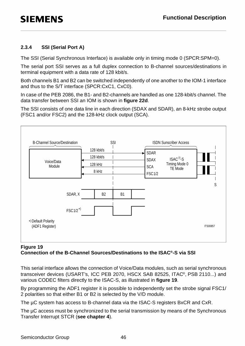
(e) C×C1, C×C0 = 11, IOM® Loop
µP
CxR IDP0
Pµ
SIN(ST0) ITS00867
FSC
B1 B2IDP1
Access
IDP1
IDP0 B2B1 B1B2
B2 B1
RIOM
Semiconductor Group 53

Functional Description
2.3.7 MONITOR Channel Handling
The MONITOR channel in IOM-1 mode is used for the exchange of control informationbetween the ISDN Communication Controller ICC (PEB 2070) and layer-1 devices like theISDN Burst Controller IBC (PEB 2095) or the ISDN Echo Cancellation circuit IEC (PEB 2090).
Since the ISAC-S combines the functions of the ICC and the S Bus interface Circuit SBC (PEB2080) and since the SBC does not use the MONITOR channel for data transfers, there isusually no necessity for performing MONITOR channel operations with the ISAC-S in IOM-1mode.
The implemented MONITOR handler of the ICC is however fully operational and can thereforebe used in conjunction with external layer-1 transceivers in case only the ICC part of theISAC-S is used (ADF1:TEM).
Prerequisite for data transfers over the monitor channel is an appropriate code in the MODEregister e.g. MODE:DIM2-0 = 010 or 011.
Only one byte of information at a time can be transferred between the ISAC-S and anotherdevice.
The procedure is as follows:
MONITOR Transmit Channel (MOX) register is loaded with the value to be sent in the outgoingMONITOR channel. (Bytes of the form FXH are not allowed for this purpose because of theTIC bus collision resolution procedure).
The receiving device interprets the incoming monitor value as a control/information byte, FXHexcluded. If no response is expected, the procedure is complete. If the receiving device doesreact by transmitting information to the ISAC-S, it should set the E bit to "0" and send theresponse in the monitor channel of the following frame.
The ISAC-S
– latches the value in the MONITOR channel of the frame immediately following a frame with"E=0" into MOR register.
– generates a MONITOR Status interrupt MOS (EXIR register) to indicate that the MORregister has been loaded. See figure 23.
Figure 23MONITOR Channel Protocol (IOM®-1)
ITD00868
IDP0
IDP1 X Y
X F= H
~
~
~
~0 0
E MON MONE
MOR Load, MOS Int. MOR Load, MOS Int.
MON
Semiconductor Group 54

Functional Description
2.3.8 Command/Indicate (C/I) Channel Handling
The C/I channel conveys the commands and indications between the layer-1 and layer-2 partsof the ISAC-S. This channel is available in all timing modes. Beside being accessed by theinternal layer-2 part, it can also be accessed by an external layer-2 device, e.g. to control thelayer-1 activation/deactivation procedures. This access is arbitrated via the TIC bus accessprotocol which is performed in the MONITOR channel.
The C/I channel is accessed via register CIRR (in receive direction, layer-1 to layer-2) andregister CIXR (in transmit direction, layer-2 to layer-1). The C/I code is four bits long.
A listing and explanation of the layer-1 C/I codes can be found in chapter 3.4.
In the receive direction, the code from layer-1 is continuously monitored, with an interrupt beinggenerated anytime a change occurs (ISTA:CISQ). A new code must be found in twoconsecutive IOM frames to be considered valid and to trigger a C/I code change interruptstatus (double last look criterion).
In the transmit direction, the code written in CIXR is continuously transmitted in the C/Ichannel.
2.3.9 TIC Bus Access
The arbitration mechanism implemented in the monitor channel of the IOM allows the accessof external communication controllers (up to 7) to the layer-1 functions provided in the ISAC-Sand to the D channel. (TIC bus; see figure 24). To this effect the outputs of the controllers(ICC:ISDN Communication Controller PEB 2070) are wired-or-and connected to pin IDP1, apull-up resistor being already provided in the ISAC-S. The inputs of the ICC’s are connectedto pin IDP0.
Semiconductor Group 55

Functional Description
Figure 24Applications of IOM® Bus Configuration
ITS00854
D-ChannelTelemetry/PacketCommunication
ICC (7)
(2)ICCwith D-ChannelCommunicationVoice/DataB-Channel
(1)ICCApplicationIVD LANE-Channel
Signaling
Signaling
B-ChannelVoice/DataCommunicationwith D-Channel
DCLFSCIDP1IDP0
Echo
E-Channel
CCITTS-Interface
µP
TIC-
Bus
RIOM -2
RISAC -S
Semiconductor Group 56

Functional Description
An access request to the TIC bus may either be generated by software (µP access to the C/Ichannel) or by the ISAC-S itself (transmission of an HDLC frame). A software access requestto the bus is effected by setting the BAC bit (CIXR register) to "1".
In case of an access request, the ISAC-S checks the bus accessed-bit (bit 3 of IDP1MONITOR octet, see figure 25) for the status "bus free", which is indicated by a logical "1". Ifthe bus is free, the ISAC-S transmits its individual TIC bus address programmed in STCRregister. The TIC bus is occupied by the device which sends its address error-free. If more thanone device attempts to seize the bus simultaneously, the one with the lowest address valuewins.
Figure 25MONITOR Channel Structure on IDP1
When the TIC bus is seized by the ISAC-S, the bus is identified to other devices as occupiedvia the IDP1 MONITOR channel bus accessed bit state "0" until the access request iswithdrawn. After a successful bus access, the ISAC-S is automatically set into a lower priorityclass, that is, a new bus access cannot be performed until the status "bus free" is indicated intwo successive frames.
If none of the devices connected to the IOM interface request access to the D and C/Ichannels, the TIC bus address 7 will be present. The device with this address will thereforehave access, by default, to the D and C/I channels.
Note: Bit BAC (CIXR register) should be reset by the µP when access to the C/I channels isno longer requested, to grant other devices access to the D and C/I channels.
The availability of the S/T interface D channel is indicated in bit 3 "Stop/Go" (S/G) of the IDP0MONITOR channel (figure 26).
S/G = 1 : stopS/G = 0 : go
Figure 26MONITOR Channel on IDP0
The stop/go bit is available to other layer-2 devices connected to the IOM to determine if theycan access the S/T bus D channel.
TIC Bus Address TBA2-0
01234567
Bus accessed = "1" (no TIC bus access) if– BAC = "0" (CIXR register) and– no HDLC transmission
01234567
111S/G1111
Semiconductor Group 57

Functional Description
2.4 IOM®-2 Mode Functions
2.4.1 IOM®-2 Frame Structure / Timing Modes
The IOM-2 is a generalization and enhancement of the IOM-1. While the basic frame structureis very similar, IOM-2 offers further capacity for the transfer of maintenance information. Interminal applications, the IOM-2 constitutes a powerful backplane bus offeringintercommunication and sophisticated control capabilities for peripheral modules.
The channel structure of the IOM-2 is depicted in figure 27.
Figure 27Channel Structure of IOM®-2
* The 64-kbit/s channels, B1 and B2, are conveyed in the first two octets.
* The third octet (monitor channel) is used for transferring maintenance information betweenthe layer-1 functional blocks (SBCX, IECQ) and the layer-2 controller (see chapter 2.4.4).
* The fourth octet (control channel) contains
– two bits for the 16-kbit/s D channel
– four command/indication bits for controlling activation/deactivation and for additional controlfunctions
– two bits MR and MX for supporting the handling of the MONITOR channel.
In the case of an IOM-2 interface the frame structure depends on whether TE- or non-TE modeis selected, via bit SPM in SPCR register.
Non-TE timing mode (SPM=1)
This mode is used in LT-S and LT-T applications. The frame is a multiplex of eight IOM-2 channels (figure28), each channel has the structure in figure 27.
The ISAC-S is assigned to one of the eight channels (0 to 7) via register programming (ADF1:CSEL2-0).
ITD02582
B1 B2 MONITOR D MR X
MΙC /
Semiconductor Group 58

Functional Description
Thus the data rate per subscriber connection (corresponding to one channel) is 256 kbit/s,whereas the bit rate is 2048 kbit/s. The IOM-2 interface signals are:
IDP0, 1 : 2048 kbit/sDCLK : 4096 kHz inputFSC1/2* : 8 kHz input
*Note: FSC1 and FSC2 should be connected together (see figure 12).
Additionally the ISAC-S supplies two programmable strobe signals (SDS1/2), active over theB-channels of the selected IOM channel (cf. ADF2:DxC2-0).
Figure 28Multiplexed Frame Structure of the IOM®-2 Interface in Non-TE Timing Mode
ITD00855
CH0 CH1 CH2 CH3 CH4 CH5 CH6 CH7 CH0
CH0CH7CH6CH5CH4CH3CH2CH1
B1 B2 MONITOR D C / I MMR X
125
FSC1/2
DCL
IDP0
IDP1
µs
RIOM
IOM CH0R
Semiconductor Group 59
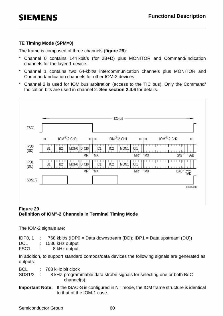
Functional Description
TE Timing Mode (SPM=0)
The frame is composed of three channels (figure 29):
* Channel 0 contains 144 kbit/s (for 2B+D) plus MONITOR and Command/Indicationchannels for the layer-1 device.
* Channel 1 contains two 64-kbit/s intercommunication channels plus MONITOR andCommand/Indication channels for other IOM-2 devices.
* Channel 2 is used for IOM bus arbitration (access to the TIC bus). Only the Command/Indication bits are used in channel 2. See section 2.4.6 for details.
Figure 29Definition of IOM®-2 Channels in Terminal Timing Mode
The IOM-2 signals are:
IDP0, 1 : 768 kbit/s (IDP0 = Data downstream (DD); IDP1 = Data upstream (DU))DCL : 1536 kHz outputFSC1 : 8 kHz output.
In addition, to support standard combos/data devices the following signals are generated asoutputs:
BCL : 768 kHz bit clockSDS1/2 : 8 kHz programmable data strobe signals for selecting one or both B/IC channel(s).
Important Note: If the ISAC-S is configured in NT mode, the IOM frame structure is identicalto that of the IOM-1 case.
ITD05968
TAD
125 µs
IPD0(DD) B1 B2 MON0 CI0 IC1 IC2 MON1 CI1D
MR MX MXMR S/G
FSC1
BACMR MXMXMR
D CI1MON1IC2IC1CI0MON0B2B1(DU)IPD1
SDS1
CH0
A/B
/2
RIOM -2 RIOM -2 CH1 RIOM -2 CH2
Semiconductor Group 60

Functional Description
2.4.2 IOM®-2 Interface Connections
Output Driver Selection
The type of the IOM output is selectable via bit ODS (ADF2 register). Thus when inactive (nottransmitting) IDP0, 1 are either high impedance (ODS=1) or open drain "1" (ODS=0).
Normally the IOM-2 interface is operated in the "open drain" mode (ODS=0) in order to takeadvantage of the bus capability. In this case pull-up resistors (1 kΩ – 5 kΩ) are required onIDP0 and IDP1.
IOM® Direction Control
For test applications, the direction of IDP0 and IDP1 can be reversed during certain timeslotswithin the IOM-2 frame. This is performed via the IDC bit in the SQXR register. For normaloperation SQXR:IDC should be set to "0".
In IOM-2 terminal mode these pull-up resistors can also be connected to FSC2/X1 pins insteadof VDD in order to reduce the power dissipation.
Semiconductor Group 61

Functional Description
Non-Terminal Mode (SPCR:SPM=1)
Outside the programmed 4-byte subscriber channel (bits CSEL2-0, ADF1 register), both IDP1and IDP0 are inactive.
Inside the programmed 4-byte subscriber channel (see figure 30):
– IDP1 carries the 2B+D channels as output towards the subscriber (i.e. to the S/T interface)and the MONITOR and C/I channel as output to the layer-1
– IDP1 is inactive during B1 and B2
– IDP0 carries the 2B+D channels coming from S/T interface, and the MONITOR and C/Ichannels from layer-1.
If IDC (IOM Direction Control, SQXR register) is set to "1", IDP0 sends the MONITOR, D andC/I channels normally carried by IDP1, i.e. normally destined to layer-1 S/T interface. Thisfeature can be used for test purposes, e.g. to send the D channel towards the system insteadof the subscriber (see figure 31).
Figure 30IOM® Data Ports 0, 1 in Non-Terminal Mode (SPCR:SPM=1) with Normal IOM® Direction (SQXR:IDC=0)
IDP0IDP1
Layer(SBC)
S/T Interface
ITS02348
IDP0IDP1
Line-CardControllere.g. EPICPEB
B1/B2
IDP0 IDP1
(ICC)
MON,
TM1
Layer 2
D, C/I2055
RISAC -S
RIOM -2 Interface
ITD03425
B1 B2 MONITOR D MR X
MΙC /
Layer
IDP1
1S / T
1
IDP0 C / Ι MXR
MDMONITORB2B1
LayerS / T Layer 2
Layer 2
RIOM
RIOM
Semiconductor Group 62

Functional Description
Figure 31IOM® Data Ports 0, 1 in Non-Terminal Mode (SPCR:SPM=1) with Reversed IOM® Direction (SQXR:IDC=1)
IDP0IDP1
Layer 1(SBC)
S/T Interface
ITS02349
IDP0IDP1
Line-CardControllere.g. EPICPEB 2055
B1/B2
IDP0 IDP1
Layer 2(ICC)
MON, D, C/I
RISAC -S
RIOM -2 Interface
R
ITD02574
B1 B2 MONITOR D MR X
MΙC /
Layer
IDP1
2S/T
2
IDP0 C / Ι MXR
MDMONITORB2B1
LayerS/T RIOM
RIOM
IOM R
IOM R
Semiconductor Group 63

Functional Description
Terminal Mode (SPM=0)
In this case the IOM has the 12-byte frame structure consisting of channels 0, 1 and 2 (seefigure 29):
– IDP0 carries the 2B+D channels from the S/T interface, and the MONITOR 0 and C/I 0channels coming from the S/T controller;
– IDP1 carries the MONITOR 0 and C/I 0 channels to the layer-1.
Channel 1 of the IOM interface is used for internal communication in terminal applications. Twocases have to be distinguished, according to whether the ISAC-S is operated as a masterdevice (communication with slave devices via MONITOR 1 and C/I 1), or as a slave device(communication with one master via MONITOR 1 and C/I 1).If IDC is set to "0" (Master Mode):
– IDP0 carries the MONITOR 1 and C/I 1 channels as output to peripheral (voice/data)devices;
– IDP0 carries the IC channels as output to other devices, if programmed (C×C1 – 0 = 01 inregister SPCR).
If IDC is set to "1" (Slave Mode):
– IDP1 carries the MONITOR 1 and C/I 1 channels as output to a master device;
– IDP0 carries the IC channels as output to other devices, if programmed (C×C1 – 0 = 01 inregister SPCR).
If required (cf. DIM2-0, MODE register), bit 5 of the last byte in channel 2 on IDP0 is used toindicate the S bus state (Stop/Go bit) and bits 2 to 5 of the last byte are used for TIC bus accessarbitration (see chapter 2.4.6).
Figure 33 shows the connection in a multifunctional terminal with the ISAC-S as a master(figure 33b) and an ICC as a slave device.
IOM®-2 Interface Power Saving Option
In order to reduce power consumption on the IOM interface to a minimum while in theoperational state the IDP0 and IDP1 pins may be connected as illustrated in figure 32. Thisoption is only available in IOM-2 terminal mode.
When programmed as open drain i/o’s, pull-ups should be connected to IDP0/1 in order toobtain a well-defined "high" voltage for a logical "1" when the driver is in high-impedance.However, a pull-up resistor connected to a static VDD has the disadvantage that power isunnecessarily dissipated (according to the R/2 law) when a "low" is output. Moreover, a staticpull-up resistor does not exploit the knowledge about the timing of the receiver at the other end.
These two disadvantages are largely avoided when using pins X1 and FSC2 for pull-ups onIDP0 and IDP1, respectively. As shown in the timing diagram in figure 32:
– X1 (FSC2) is connected to VDD when nothing is being transmitted on IDP0 (IDP1)
– X1 (FSC2) is not connected when a "0" is being output on IDP0 (IDP1) (which has the effectof reducing the power consumption practically to "0" during this time)
– X1 (FSC2) is connected to VDD when a "1" is to be transmitted and is indeed being latchedby the destination.
Semiconductor Group 64

Functional Description
X1 and FSC2 are driven between the first and the second falling edge of the DCL signal. They are always not connected between the first rising and the first falling edge as well as the second falling and the first rising edge.
Note: This feature should not be used if a PSB 2186 ISAC-S TE is considered to replace thePEB 2085/2086.
Figure 32IOM®-2 Connections for Power Saving Option
IOM® OFF Function
In IOM-2 terminal mode (SPCR:SPM=0) the IOM interface can be switched off for externaldevices via IOF bit in ADF1 register. If IOF=1, the interface is switched off i.e. DCL, FSC1,IDP0/1 and BCL are high impedance.
ITD02347
VDD
N.C.
X1
IDP0 (O.D.)
(O.D.)IDP1
FSC2
N.C. = Not Connected
X1
FSC2
IDP0
IDP1
N.C.
DDV
VDD
N.C.N.C.
DDV
VDD
0 V
V0
DDV
DCL
Semiconductor Group 65

Functional Description
Figure 33aIOM® Data Ports 0, 1 in Terminal Mode (SPCR:SPM=0)
IDP0IDP1
Layer 1(SBC)
ITS02355
IDP0IDP1
IDP0 IDP1
Layer 2(ICC)
ModuleVoice/Data
IDP1IDP0 e.g. PEB 2070(ICC) in SlaveMode (IDC=1)
in MasterMode(IDC = 0)
C
MON1, C/I1, IC1, IC2
2B+D, C/I0, MON0, S/G, TIC
Master Slave
S/TInterface
µ
(DU)(DD)
(DD) (DU)
RISAC -S
ISAC -SR
RIOM -2 Interface
Semiconductor Group 66

Functional Description
Figure 33b
ITD05415
TIC-Bus
IPD0(DD) B1 B2 MON0 CI0 IC1 IC2 MON1 CI1D
MR MX MXMR S/G
BACMR MXMXMR
D CI1MON1IC2IC1CI0MON0B2B1(DU)IPD1
CH0 CH1 CH2A/B
TAD
S/T IC Transmitif Progr.Layer Layer1 2 Layer 2
2Layer12 LayerLayer if Progr.IC ReceiveS/T
S/T IC Transmitif Progr.Layer Layer2 1
Layer 2
2Layer
21 LayerLayer if Progr.S/T
TAD
CH2CH1CH0
IPD1(DU) B1 B2 MON0 CI0 IC1 IC2 MON1 CI1D
MR MX MXMR BAC
MR MXMXMR
D CI1MON1IC2IC1CI0MON0B2B1(DD)IPD0
TIC-Bus
A/BS/G
RIOM -2
IOM R -2
RIOM -2
-2IOM R
IOM R -2
-2IOM R
IOM R -2
IOM R -2
Semiconductor Group 67

Functional Description
2.4.3 µP Access to B and IC Channels
In IOM-2 terminal mode (TE mode, SPCR:SPM=0) the microprocessor can access the B andIC (intercommunication) channels at the IOM-2 interface by reading the B1CR/B2CR or byreading and writing the C1R/C2R registers. Furthermore it is possible to loop back theB-channels from/to the S/T interface or to loop back the IC channels from/to the IOM-2interface without µP intervention.
These access and switching functions are selected with the Channel Connect bits (CxC1,CxC0) in the SPCR register (table 4, figure 34).
External B-channel sources (voice/data modules) connected to the IOM-2 interface can bedisconnected with the IOM off function (ADF1:IOF) in order to not disturb the B-channel access(see figure 34).
If the B-channel access is used for transferring 64 kbit/s voice/data information directly fromthe µP port to the ISDN S/T interface, the access can be synchronized to the IOM interface bymeans of a synchronous transfer interrupt programmed in the STCR register.
Table 4µP Access to B/IC Channels (IOM®-2)
Note: x=1 for channel 1 or 2 for channel 2
The general sequence of operations to access the B/IC channels is:
C×C1 ApplicationsC×C0
Read Write Read
0 B× monitoring, IC× monitoring0 IC× – B×
0 B× monitoring, IC× looping from/to IOM-21 IC× IC× B×
1 B× access from/to S0;transmission of a constant value inB× channel to S0
0 – B× B×
1 B× looping from S0;transmission of a variable pattern inB× channel to S0
1 B× B× –
C×R B×CR
IOM-2
–
IC×
B×
B×
OutputC×R
to
(set configuration register SPCR)
Program Synchronous Interrupt (ST0)
SIN – > Read Register (B×CR, C×R)(Write register)
Acknowledge SIN (SC0)
Semiconductor Group 68
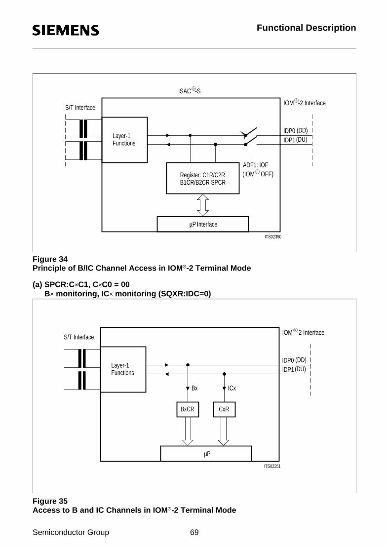
Functional Description
Figure 34Principle of B/IC Channel Access in IOM®-2 Terminal Mode
(a) SPCR:C×C1, C×C0 = 00B× monitoring, IC× monitoring (SQXR:IDC=0)
Figure 35Access to B and IC Channels in IOM®-2 Terminal Mode
IDP0IDP1
Layer-1Functions
S/T Interface
ITS02350
P Interface
ADF1:
Register: C1R/C2RB1CR/B2CR SPCR
µ
IOF
(DU)(DD)
RISAC -S
R(IOM OFF)
RIOM -2 Interface
BxCR
Layer-1Functions
S/T Interface
ITS02351
P
Bx
CxR
ICx
µ
IDP1IDP0 (DD)
(DU)
RIOM -2 Interface
Semiconductor Group 69

Functional Description
(b) SPCR:C×C1, C×C0 = 01B× monitoring, IC× looping (SQXR:IDC=0)
(c) SPCR:C×C1, C×C0 = 10B× access from/to S/Ttransmission of constant value to S/T
BxCR
ITS02352
P
ICxBx
CxR
S/T Interface
Layer-1Functions
µ
IDP1IDP0 (DD)
(DU)
RIOM -2 Interface
BxCR
ITS02353
P
Bx
CxR
Bx
S/T Interface
Layer-1Functions
µ
IDP1IDP0 (DD)
(DU)
RIOM -2 Interface
Semiconductor Group 70

Functional Description
(d) SPCR:C×C1, C×C0 = 11B× looping from/to S/Ttransmission of variable pattern to S/T
2.4.4 MONITOR Channel Handling
In IOM-2 mode, the MONITOR channel protocol is a handshake protocol used for high speedinformation exchange between the ISAC-S and other devices, in MONITOR channel "0" or "1"(see figure 29). In the non-TE mode, only one MONITOR channel is available ("MONITORchannel 0").
The MONITOR channel protocol is necessary:
For programming and controlling devices attached to the IOM. Examples of such devicesare: layer-1 transceivers (using MONITOR channel 0), and peripheral V/D modules that donot need a parallel microcontroller interface (monitor channel 1), such as the Audio RingingCodec Filter PSB 2160.
For data exchange between two microcontroller systems attached to two different deviceson one IOM-2 backplane. Use of the MONITOR channel avoids the necessity of a dedicatedserial communication path between the two systems. This greatly simplifies the systemdesign of terminal equipment (figure 36).
Note: There is normally no necessity for monitor channel operations over "MONITOR channel0" since the internal layer-1 part of the ISAC-S does not support this function. Theimplemented MONITOR handler can however be used with external layer-1transceivers in case only the ICC part of the ISAC-S is used (ADF1:TEM).
CxR
ITS02354
P
BxBx
µ
S/T Interface
Layer-1Functions IDP1
IDP0 (DD)(DU)
RIOM -2 Interface
Semiconductor Group 71

Functional Description
Figure 36Examples of MONITOR Channel Applications in IOM®-2 TE Mode
The MONITOR channel operates on an asynchronous basis. While data transfers on the bustake place synchronized to frame sync, the flow of data is controlled by a handshake procedureusing the MONITOR Channel Receive (MR0 or 1) and MONITOR Channel Transmit (MX0 or1) bits. For example: data is placed onto the MONITOR channel and the MX bit is activated.This data will be transmitted repeatedly once per 8-kHz frame until the transfer isacknowledged via the MR bit.
The microprocessor may either enforce a "1" (idle) in MR, MX by setting the control bit MRC1,0 or MXC1, 0 to "0" (MONITOR Control Register MOCR), or enable the control of these bitsinternally by the ISAC-S according to the MONITOR channel protocol. Thus, before a dataexchange can begin, the control bit MRC(1, 0) or MXC(1, 0) should be set to "1" by themicroprocessor.
The MONITOR channel protocol is illustrated in figure 37. Since the protocol is identical inMONITOR channel 0 and MONITOR channel 1 (available in TE mode only), the index 0 or 1has been left out in the illustration.
The relevant status bits are:
In addition, the status bit:
MONITOR Channel Active MAC (MAC0, MAC1)indicates whether a transmission is in progress (Register: STAR).
ITS00869
V/D - Module
PSB
ARCOFI
ARCOFI 2160
21652085/86PEB2110PSB
V/D - Module
Cµ µC
Control (MONITOR1)Data Communication (MONITOR1)
RIOM -2
RITACR
-SP PSBR
RISAC -S
MONITOR Channel Data Received MDR (MDR0, MDR1)MONITOR Channel End of Reception MER (MER0, MER1)
for the reception of MONITOR data, and
MONITOR Channel Data Acknowledged MDA (MDA0, MDA1)MONITOR Channel Data Abort MAB (MAB0, MAB1)
for the transmission of MONITOR data (Register: MOSR)
Semiconductor Group 72
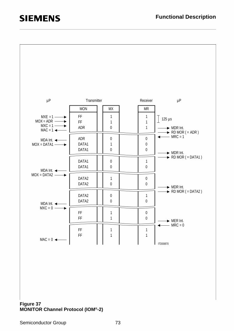
Functional Description
Figure 37MONITOR Channel Protocol (IOM®-2)
ITD00870
MON MX
Transmitter
MR
11FFFF 1 1ADR 0 1
00DATA101DATA1
ADR 0 0
DATA1 0 1DATA1 0 0
00DATA201DATA2
DATA2 0 1DATA2 0 0
FF 1 0FF 1 0
FF 1 1FF 1 1
Receiver
MXE = 1ADR=MOX
MXC = 11=MAC
MOX = DATA1MDA Int.
MDA Int.DATA2=MOX
MDA Int.0=MXC
0=MAC
MDR Int.RDMRC
MOR= 1
( = ADR )
DATA1 )( =MORRDMDR Int.
MDR Int.RD MOR ( = DATA2 )
MRC = 0MER Int.
125 s
PPµ µ
µ
Semiconductor Group 73

Functional Description
Before starting a transmission, the microprocessor should verify that the transmitter is inactive,i.e. that a possible previous transmission has been terminated. This is indicated by a "0" in theMONITOR Channel Active MAC status bit.
After having written the MONITOR Data Transmit (MOX) register, the microprocessor sets theMONITOR Transmit Control bit MXC to "1". This enables the MX bit to go active (0), indicatingthe presence of valid MONITOR data (contents of MOX) in the corresponding frame. As aresult, the receiving device stores the MONITOR byte in its MONITOR Receive MOR registerand generates an MDR interrupt status.
Alerted by the MDR interrupt, the microprocessor reads the MONITOR Receive (MOR)register. When it is ready to accept data (e.g. based on the value in MOR, which in a point-to-multipoint application might be the address of the destination device), it sets the MR control bitMRC to "1" to enable the receiver to store succeeding MONITOR channel bytes andacknowledge them according to the MONITOR channel protocol. In addition, it enables otherMONITOR channel interrupts by setting MONITOR Interrupt Enable to "1".
As a result, the first MONITOR byte is acknowledged by the receiving device setting the MRbit to "0". This causes a MONITOR Data Acknowledge MDA interrupt status at the transmitter.
A new MONITOR data byte can now be written by the microprocessor in MOX. The MX bit isstill in the active (0) state. The transmitter indicates a new byte in the MONITOR channel byreturning the MX bit active after sending it once in the inactive state. As a result, the receiverstores the MONITOR byte in MOR and generates a new MDR interrupt status. When themicroprocessor has read the MOR register, the receiver acknowledges the data by returningthe MR bit active after sending it once in the inactive state. This in turn causes the transmitterto generate an MDA interrupt status.
This "MDA interrupt – write data – MDR interrupt – read data – MDA interrupt" handshake isrepeated as long as the transmitter has data to send. Note that the MONITOR channel protocolimposes no maximum reaction times to the microprocessor.
When the last byte has been acknowledged by the receiver (MDA interrupt status), themicroprocessor sets the MONITOR Transmit Control bit MXC to "0". This enforces an inactive("1") state in the MX bit. Two frames of MX inactive signifies the end of a message. Thus, aMONITOR Channel End of Reception MER interrupt status is generated by the receiver whenthe MX bit is received in the inactive state in two consecutive frames. As a result, themicroprocessor sets the MR control bit MRC to 0, which in turn enforces an inactive state inthe MR bit. This marks the end of the transmission, making the MONITOR Channel ActiveMAC bit return to "0".
During a transmission process, it is possible for the receiver to ask a transmission to beaborted by sending an inactive MR bit value in two consecutive frames. This is effected by themicroprocessor writing the MR control bit MRC to "0". An aborted transmission is indicated bya MONITOR Channel Data Abort MAB interrupt status at the transmitter.
2.4.5 C/I Channel Handling
The Command/Indication channel carries real-time status information between the ISAC-Sand another device connected to the IOM.
1) One C/I channel (called C/I0) conveys the commands and indications between the layer-1and the layer-2 parts of the ISAC-S. This channel is available in all timing modes (TE and
Semiconductor Group 74

Functional Description
non-TE). It can be accessed by an external layer-2 device e.g. to control the layer-1activation/deactivation procedures. C/I0 channel access may be arbitrated via the TIC busaccess protocol in the IOM-2 terminal timing mode (SPCR:SPM=0). In this case thearbitration is done in C/I channel 2 (see figure 29).
The C/I0 channel is accessed via register CIR0 (in receive direction, layer-1 to layer-2) andregister CIX0 (in transmit direction, layer-2 to layer-1). The C/I0 code is four bits long.
A listing and explanation of the layer-1 C/I codes can be found in chapter 3.4.
In the receive direction, the code from layer-1 is continuously monitored, with an interruptbeing generated anytime a change occurs (ISTA:CISQ). A new code must be found in twoconsecutive IOM frames to be considered valid and to trigger a C/I code change interruptstatus (double last look criterion).
In the transmit direction, the code written in CIX0 is continuously transmitted in C/I0.
2) A second C/I channel (called C/I1) can be used to convey real time status informationbetween the ISAC-S and various non-layer-1 peripheral devices e.g. PSB 2160 ARCOFI.The channel consists of six bits in each direction. It is available only in the IOM-2 TE timingmode (see figure 29).
The C/I1 channel is accessed via registers CIR1 and CIX1. A change in the received C/I1code is indicated by an interrupt status without double last look criterion.
Semiconductor Group 75

Functional Description
Figure 38Applications of TIC Bus in IOM®-2 Bus Configuration
2.4.6 TIC Bus Access
In IOM-2 interface mode the TIC bus capability is only available in TE mode. The arbitrationmechanism implemented in the last octet of IOM channel 2 of the IOM allows the access ofexternal communication controllers (up to 7) to the layer-1 functions provided in the ISAC-Sand to the D channel. (TIC bus; see figure 38). To this effect the outputs of the controllers(ICC:ISDN Communication Controller PEB 2070) are wired-or-and connected to pin IDP1. Theinputs of the ICCs are connected to pin IDP0. External pull-up resistors on IDP0/1 are required.The arbitration mechanism must be activated by setting MODE:DIM2–0=001 (seechapter 4.1.7).An access request to the TIC bus may either be generated by software (µP access to the C/I
ITS00854
D-ChannelTelemetry/PacketCommunication
ICC (7)
(2)ICCwith D-ChannelCommunicationVoice/DataB-Channel
(1)ICCApplicationIVD LANE-Channel
Signaling
Signaling
B-ChannelVoice/DataCommunicationwith D-Channel
DCLFSCIDP1IDP0
Echo
E-Channel
CCITTS-Interface
µP
TIC-
Bus
RIOM -2
RISAC -S
Semiconductor Group 76

Functional Description
channel) or by the ISAC-S itself (transmission of an HDLC frame). A software access requestto the bus is effected by setting the BAC bit (CIX0 register) to "1".
In the case of an access request, the ISAC-S checks the Bus Accessed-bit (bit 5 of IDP1 lastoctet of Ch2, see figure 39) for the status "bus free", which is indicated by a logical "1". If thebus is free, the ISAC-S transmits its individual TIC bus address programmed in the STCRregister. The TIC bus is occupied by the device which sends its address error-free. If more thanone device attempt to seize the bus simultaneously, the one with the lowest address valueswins.
Figure 39Structure of Last Octet of Ch2 on IDP1 (DU)
When the TIC bus is seized by the ISAC-S, the bus is identified to other devices as occupiedvia the IDP1 Ch2 Bus Accessed-bit state "0" until the access request is withdrawn. After asuccessful bus access, the ISAC-S is automatically set into a lower priority class, that is, a newbus access cannot be performed until the status "bus free" is indicated in two successiveframes.
If none of the devices connected to the IOM interface request access to the D and C/Ichannels, the TIC bus address 7 will be present. The device with this address will thereforehave access, by default, to the D and C/I channels.
Note: Bit BAC (CIX0 register) should be reset by the µP when access to the C/I channels isno more requested, to grant other devices access to the D and C/I channels.
The availability of the S/T interface D channel is indicated in bit 5 "Stop/Go" (S/G) of the IDP0last octet of Ch2 channel (figure 40).
S/G = 1 : stopS/G = 0 : go
ITD02575
D CI1MON1IC2IC1CI0MON0B2B1
MRMX MX
MR TADBAC
TADBAC
1 02
TIC-Bus AddressBus Accessed
(TAD 2-0)(’1’ no TIC-Bus Access)
Semiconductor Group 77

Functional Description
Figure 40Structure of Last Octet of Ch2 on IDP0 (DD)
The stop/go bit is available to other layer-2 devices connected to the IOM to determine if theycan access the S/T bus D channel.
ITD05422
D CI1MON1IC2IC1CI0MON0B2B1
MRMX MX
MR
S/G A/B
A/BS/G
STOP/GO Available/Blocked
Semiconductor Group 78
Functional Description
2.5 Layer-1 Functions for the S/T Interface
The common functions in all operating modes are:
– line transceiver functions for the S/T interface according to the electrical specifications ofCCITT I.430;
– conversion of the frame structure between IOM and S/T interface;
– conversion from/to binary to/from pseudo-ternary code;
– level detect.
Mode specific functions are:
– receive timing recovery for point-to-point, passive bus and extended passive busconfiguration;
– S/T timing generation using IOM timing synchronous to system, or vice versa;
– D-channel access control and priority handling;
– D-channel echo bit generation by handling of the global echo bit;
– activation/deactivation procedures, triggered by primitives received over the IOM C/Ichannel or by INFO's received from the line;
– execution of test loops.
For a block diagram, see figure 10.
The wiring configurations in user premises, in which the ISAC-S can be used are illustrated infigure 41.
Semiconductor Group 79

Functional Description
Figure 41Wiring Configurations in User Premises
TE
TR TR
TRTR
LT-T
Point-to-PointConfigurationsSBC
LT-S
NT
NT
LT-S
SBCTR TRShort PassiveBus
ITS00860
TE1 TE8
1) The maximum line attenuation toleratet by the ISAC dB at 96 kHz.
1.5 km1)
150 m
m10
10 m
m500
TE8TE1
Passive BusExtended
TRTR SBC
LT-S
NT
m35
TR: Terminating Resistor
_<
km_< 1.5 1)
RISAC -S
RISAC -S
R -S is 15
ISAC R -S
RIOM
ISAC -SR
IOM R
_<
_<
ISAC -SR
ISAC -SRISAC -SR
IOM R
_<
_<
ISAC -SRISAC -SR
_<
Semiconductor Group 80

Functional Description
2.5.1 S/T Interface
According to CCITT recommendation I.430 pseudo-ternary encoding with 100% pulse width isused on the S/T interface. A logical "1" corresponds to a neutral level (no current), whereaslogical "0" ’s are encoded as alternating positive and negative pulses. An example is shown infigure 42.
Figure 42S/T Interface Line Code
One frame consists of 48 bits, at a nominal bit rate of 192 kbit/s. Thus each frame carries twooctets of B1, two octets of B2, and four D-bits, according to the B1+B2+D structure defined forthe ISDN basic access (total useful data rate: 144 kbit/s). Frame begin is marked using a codeviolation (no Mark inversion). The frame structures (from network to subscriber, and subscriberto network) are shown in figure 43.
Figure 43Frame Structure at Reference Points S and T (CCITT I.430)
Note: Dots demarcate those parts of the frame that are independently DC-balanced.
ITD00322
0 1 0 0 1 1 0 0 0 1 1V+
0 V
V-
ITD02330
DL.
010
L.F B1 E D A F NA B2 E D M B1 SDE B2 E D L. F L.
48 Bits in 250 µs
L.FL.DL.B2L. D L.B1L.DL.B2A L.FL.DL.B1F L.L.D
F = Framing BitDC Balancing Bit=LD-Channel Bit=DD-Echo-Channel Bit=EAuxiliary Framing Bit or Q-Bit=FA
Bit set to a Binary Value N=NB1 = Bit within B ChannelB2 =A = Bit used for ActivationS = Subchannel SC1 through SC5 bit positionM = Multiframing Bit
Bit within B Channel
t
FA=12
2 Bits Offset
NT TE
NTTE010
Semiconductor Group 81

Functional Description
2.5.2 Analog Functions
For both receive and transmit direction, a 2:1 transformer is used to connect the ISAC-Stransceiver to the 4 wire S/T interface. The connections are shown in figure 44 .
Figure 44Connection of the Line Transformers and Power Supply to the ISAC ®-S
The external transformer of ratio 2:1 is needed in both receive and transmit direction to providefor isolation and transform voltage levels according to CCITT recommendations.
The equivalent circuits of the integrated receiver and transmitter are shown in figure 45 .
The full-bauded pseudo-ternary pulse shaping is achieved with the integrated transmitterwhich is realized as a current limited voltage source. A voltage of 2.1 V is delivered betweenSX1-SX2, which yields a current of 7.5 mA over 280 Ω.
ITS02339
+ 5 V
10 µF
GND
2 : 1
2 : 1
Pair
Pair
VDD
SX1
SX2
SR1
SR2
VSSD
VSSA
PEB 2085
Transmit
Receive
ITS05640
+ 5 V
10 µF
GND
2 : 1
2 : 1
Pair
Pair
VDD
SX1
SX2
SR1
SR2
VSSD
VSSA
PEB 2086
Transmit
Receive
Semiconductor Group 82

Functional Description
Figure 45Equivalent Internal Circuits of Receiver and Transmitter Stages
The transmitter of the PEB 2086 ISAC-S is identical to that of both the PEB 2080 SBC andPEB 2085 ISAC-S, hence, the line interface circuitry should be the same. The externalresistors (20 ... 40 Ω) are required in order to adjust the output voltage to the pulse mask(nominal 750 mV according CCITT I.430, to be tested with the command "TM1") on the onehand and in order to meet the output impedance of minimum 20 Ω (tansmission of a binary oneaccording to CCITT I.430, to be tested with the command "TM2") on the other hand.
The S-bus receiver of the PEB 2085 is designed as a threshold detector with adaptivelyswitched threshold levels. Pin SR1 delivers 2.5 V as an output, which is the virtual ground ofthe input signal on pin SR2.
The S-bus receiver of the PEB 2086 has been changed to a symmetrical one. This results ina simplification of the external circuitry and PCB layout to meet the I.430 receiver inputimpedance specification.
ITS02357
SR1
SR2
UF1
k1<2.5
+
_
ΩV
PEB 2085RISAC -S
ITS02358
SX1
SX2
2.1
2.1
13.4Ι mA
V
V
2085PEB
_<
RISAC -S
ITS05630
SR1k40
+
_
Ω
SR2
Ω50 k
Ω40 k
50 kΩ
2.5V
2086PEBRIOM -S
ITS02358
SX1
SX2
2.1
2.1
13.4Ι mA
V
V
2085PEB
_<
RISAC -S
Semiconductor Group 83

Functional Description
2.5.3 S/T Interface Circuitry
2.5.3.1 S/T Interface Pre-Filter (PEB 2085 only)
In some applications it may be desirable to improve the signal-to-noise ratio of the receivedS/T interface signal by filtering out undesirable frequency (usually high frequency)components. This may be realized by an external pre-filter.
To simplify the implementation of this filter, an operational amplifier is integrated in thePEB 2085, as shown in figure 46. By connecting an RC network between input SR2 and theextra pin UFI an active RC filter of desired order can be realized (one example is shown infigure 46).
Figure 46Prefilter Connections and Example of 2nd Order RC Network
Following component values are recommended to give a 500 kHz cutoff, and 600 ns(± 170 ns) propagation delay time:
R1 = R2 = 10 kΩC1 = 13 pFC2 = 22.5 pF
Delay Compensation (PEB 2085 and PEB 2086)
To compensate for the extra delay introduced into the received signal by a filter, the samplingof the receive signal can be delayed by programming bits TEM and PFS in the ADF1 registeras shown in table 5. Note that setting TEM to "1" and PFS to "0" has the effect of completelydisabling layer-1 functions, for test purposes (see section 2.7).
ITS02359
VSSA
UFI
SR2
10
SR1
RCNetwork
A
nF
_
+
ITS02360
C2
R1
VSSA
2R
1C
SR2
UF1
A
RC Network Example
Semiconductor Group 84

Functional Description
Table 5TEM/PFS Function Table
This delay compensation might be necessary in order to comply with the "total phase deviationinput to output" requirement of CCITT recommendation I.430 which specifies a phasedeviation in the range of – 7% to + 15% of a bit period.
2.5.3.2 External Protection Circuitry
The CCITT specification for both transmitter and receiver impedances in TEs results in aconflict with respect to external S0-protection circuitry requirements:
• To avoid destruction or malfunctioning of the S0-device it is desirable to drain off even smallovervoltages reliably.
• To meet the 96 kHz impedance test specified for transmitters and receivers (for TEs only,CCITT sections 8.5.1.2a and 8.6.1.1) the protection circuit must be dimensioned such thatvoltages below 2.4 V are not affected (1.2 V CCITT amplitude x transformer ratio 1:2).
This requirement results from the fact that this test is to be performed with no supply voltagebeing connected to the TE. Therefore the second reference point for overvoltages VDD, istied to GND. Then, if the amplitude of the 96 kHz test signal is greater than the combinedforward voltages of the diodes, a current exceeding the specified one may pass theprotection circuit.
The following recommendations aim at achieving the highest possible device protectionagainst overvoltages while still fulfilling the 96 kHz impedance tests.Depending on transformer and circuit layout, it may become necessary to rise the thresholdvoltage slightly.
If the device is not used in TE applications, the Zener diodes should be replaced by standarddiodes.
TEM PFS Effect
0 0 No pre-filter (0 delay)
0 1 Pre-filter delay compensation 520 ns
1 1 Pre-filter delay compensation 910 ns
1 0 Test mode (layer-1 disabled)
Semiconductor Group 85
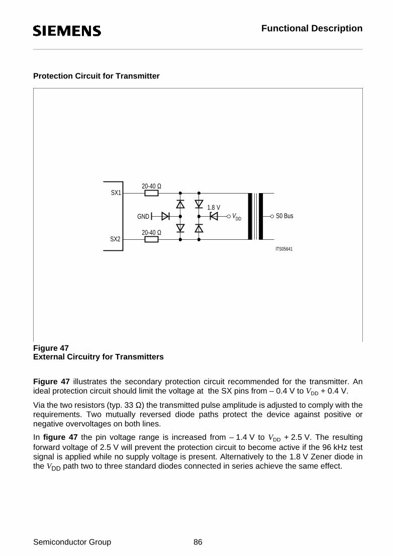
Functional Description
Protection Circuit for Transmitter
Figure 47External Circuitry for Transmitters
Figure 47 illustrates the secondary protection circuit recommended for the transmitter. Anideal protection circuit should limit the voltage at the SX pins from – 0.4 V to VDD + 0.4 V.
Via the two resistors (typ. 33 Ω) the transmitted pulse amplitude is adjusted to comply with therequirements. Two mutually reversed diode paths protect the device against positive ornegative overvoltages on both lines.
In figure 47 the pin voltage range is increased from – 1.4 V to VDD + 2.5 V. The resultingforward voltage of 2.5 V will prevent the protection circuit to become active if the 96 kHz testsignal is applied while no supply voltage is present. Alternatively to the 1.8 V Zener diode inthe VDD path two to three standard diodes connected in series achieve the same effect.
ITS05641
DDV
20-40 Ω
Ω20-40SX1
SX2
S0 Bus1.8 V
GND
Semiconductor Group 86

Functional Description
Protection Circuit for Unsymmetrical Receivers (PEB 2085)
For unsymmetrical S0-receivers (PEB 2085) a 2.5 V reference voltage is supplied at pin SR1(output). The input signal at pin SR2 is referred to the level at pin SR1. In order to stabilize thereference voltage, a 10 nF capacitor is used. Resistors between pin SR 1 and the transformershould be avoided. Sometimes, however, a small resistor is required to improve theLongitudinal Conversion Loss (LCL) performance; absolute maximum is 200 Ω.
At pin SR2 a low-pass filter of 1st or 2nd order may be provided to reject high frequency noise.The overall impedace, however, should not exceed 10 kΩ to avoid input signal reduction dueto voltage division in conjunction with the internal impedance. In case no low-pass filter isrequired the resistor may be omitted.
Figure 48External Circuitry for Unsymmetrical Receivers (PEB 2086)
The recommended protection circuit of figure 48 is widely identical to that of the transmitter(figure 47). This is necessary because no current limiting resistor of the desired dimensionmay be introduced in the SR1 path.
The RC combination on the line side centre tap of the transformer compensates the LCL dropin the frequency range between 200 kHz and 300 kHz. This drop is a consequence of the10 nF capacitor at SR1 (which cannot be omitted). The resistor in this RC combination limitsthe current through the capacitor when overvoltages are applied. This normally allows using acapacitor rated at 400 V.
The resonance frequency of the RC combination must be matched to suite specificcompensation requirements.
ITS05642
10 nF
SR2
SR1
pF47
< 10 Ωk
S0 BusV1.8
VDD
1.5 nF
2.2 kΩ
GND
Semiconductor Group 87

Functional Description
Protection Circuit for Symmetrical Receivers
Figure 49 illustrates the external circuitry used in combination with a symmetrical receiver(PEB 2086 ISAC-S) Protection of symmetrical receivers is rather comfortable.
Figure 49External Circuitry for Symmetrical Receivers
Between each receive line and the transformer a 10 kΩ resistor is used. This value is split intotwo resistors: one between transformer and protection diodes for current limiting during the96 kHz test, and the second one between input pin and protection diodes to limit the maximuminput current ot the chip.
With symmetrical receivers no difficulties regarding LCL measurements are observed;compensation networks thus are obsolete.
In order to comply to the physical requirements of CCITT recommendation I.430 andconsidering the national requirements concerning overvoltage protection and electromagneticcompability (EMC), the ISAC-S needs additional circuitry. Useful hints of how to design suchinterface circuitry are also contained in the Application Note "S/T interface circuitry using thePEB 2080 SBC or PEB 2085 ISAC-S".
2.5.4 Receiver Functions
ITS05643
DDV
1.8 Ωk
kΩ1.8
47 pF
SR2
SR1
pF47
8.2 Ωk
kΩ8.2
S0 BusGND
Semiconductor Group 88

Functional Description
2.5.4.1 Receive Signal Oversampling
In order to additionally reduce the bit error rate in severe conditions, the ISAC-S performsoversampling of the received signal and uses majority decision logic. (Note: this feature isimplemented in TE and LT-T modes only).
As illustrated in figure 50, each received bit is sampled 29 times at 7.68-MHz clock intervalsinside the estimated bit window. The samples obtained are compared against a thresholdVTR1 or VTR2 (see section: Adaptive Receiver Characteristics).
If at least 16 samples have an amplitude exceeding the selected threshold, a logical "0" isconsidered to be detected, otherwise a logical "1" (no signal) is considered detected.
Figure 50S/T Receive Signal Oversampling
ITD02361
27 30 312421 22 26 2920 23118 171497 12 191813 15 161 43 5 62 33 353432 40393837362825
VSR2 SR1V
VTR1 TR2V
Derived 192-kHz Receive Bit Period10
-
or
0 V
Semiconductor Group 89

Functional Description
2.5.4.2 Adaptive Receiver Characteristics
The integrated receiver uses an adaptively switched threshold detector. The detector controlsthe switching of the receiver between two sensitivity levels. The hysteresis characteristics ofthe receiver are shown in figure 51.
Figure 51Switching of the Receiver between High Sensitivity and Low Sensitivity
ITD00774
+ 225 mV
mV- 225
V0
0Logical
Logical 0
1Logical
VSR2 - SR1V VSR1-SR2V
Logical 1
0Logical
Logical 0
0 V
- 375 mV
mV+ 375
State 1High Sensitivity
with TR1V ± 225 mV= = mV± 375VTR2withLow Sensitivity
2State
1 2
maxV > 1 V or V-1<V max
in two Consecutive Frames
maxV > -750 mVandmV750<V maxmaxV 1 V750 mV
V SR1-SR2VV TR1 TR2V
==
=maxV V SR2 - SR1V
Input VoltageThreshold Voltages of the Receiver Threshold Detector
Maximum Value of during one Frame
_<_< <_<_ 750 max_<_mV V< _<<_ V1
Semiconductor Group 90

Functional Description
2.5.4.3 Level Detection Power Down (TE mode)
In power down state, (see chapter 3.3.1) only an analog level detector is active. All clocks,including the IOM interface, are stopped. The data lines are "high", whereas the clocks are"low".
An activation initiated from the exchange side (Info 2 on S-bus detected) will have theconsequence that a clock signal is provided automatically.
From the terminal side an activation must be started by setting and resetting the SPU-bit in theSPCR register (see chapter 4).
2.5.5 Timing Recovery
NT and LT-S
In NT and LT-S modes, the 192-kHz transmit bit clock is synchronized to the IOM clock. In thereceive direction two cases have to be distinguished depending on whether a bus or a point-to-point operation is programmed in ADF1 (IOM-1) or SQXR (IOM-2) register (see figure 52):
– In a bus configuration (CFS=1), the 192-kHz receive bit clock is identical to the transmit bitclock, shifted by 4.6 µs with respect to the transmit edge. According to CCITT I.430, thereceive frame shall be shifted by two bits with respect to the transmit frame.
– In a point-to-point or extended passive bus configuration (CFS=0), the 192-kHz receive bitclock is recovered from the receive data stream on the S interface. The sampling instant forthe receive bits is shifted by 3.9 µs with respect to the leading edge of the derived receiveclock. According to CCITT I.430, the receive frame can be shifted by 2-8 bits with respectto the transmit frame at the LT-S (NT). However, note that other shifts are also allowed bythe ISAC-S (including 0).
Semiconductor Group 91
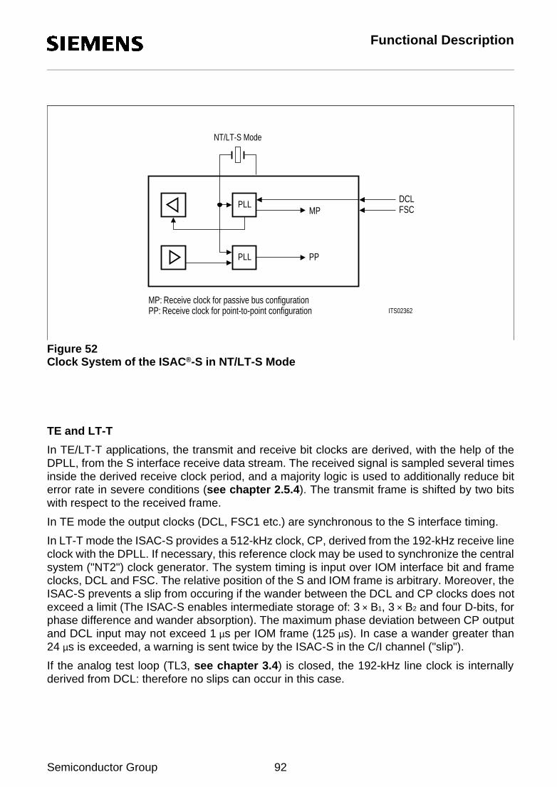
Functional Description
Figure 52Clock System of the ISAC®-S in NT/LT-S Mode
TE and LT-T
In TE/LT-T applications, the transmit and receive bit clocks are derived, with the help of theDPLL, from the S interface receive data stream. The received signal is sampled several timesinside the derived receive clock period, and a majority logic is used to additionally reduce biterror rate in severe conditions (see chapter 2.5.4). The transmit frame is shifted by two bitswith respect to the received frame.
In TE mode the output clocks (DCL, FSC1 etc.) are synchronous to the S interface timing.
In LT-T mode the ISAC-S provides a 512-kHz clock, CP, derived from the 192-kHz receive lineclock with the DPLL. If necessary, this reference clock may be used to synchronize the centralsystem ("NT2") clock generator. The system timing is input over IOM interface bit and frameclocks, DCL and FSC. The relative position of the S and IOM frame is arbitrary. Moreover, theISAC-S prevents a slip from occuring if the wander between the DCL and CP clocks does notexceed a limit (The ISAC-S enables intermediate storage of: 3 × B1, 3 × B2 and four D-bits, forphase difference and wander absorption). The maximum phase deviation between CP outputand DCL input may not exceed 1 µs per IOM frame (125 µs). In case a wander greater than24 µs is exceeded, a warning is sent twice by the ISAC-S in the C/I channel ("slip").
If the analog test loop (TL3, see chapter 3.4) is closed, the 192-kHz line clock is internallyderived from DCL: therefore no slips can occur in this case.
ITS02362
DCLFSCMP
PPPLL
PLL
MP:PP:
Receive clock for passive bus configurationReceive clock for point-to-point configuration
NT/LT-S Mode
Semiconductor Group 92
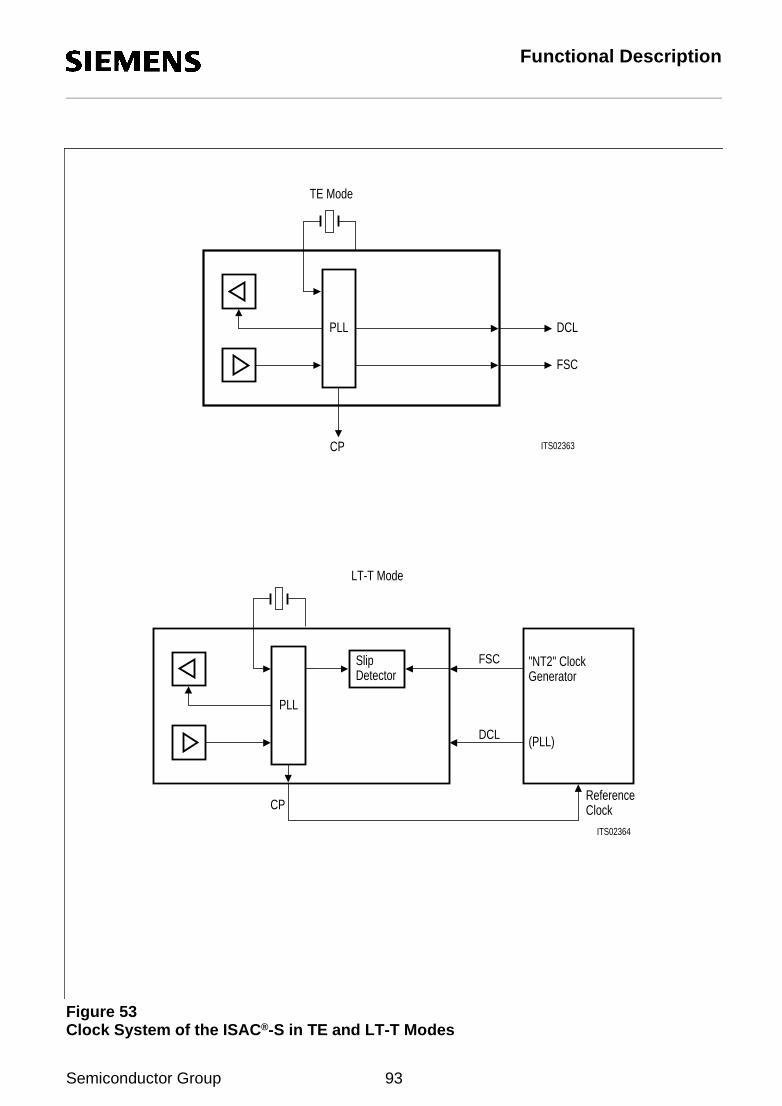
Functional Description
Figure 53Clock System of the ISAC®-S in TE and LT-T Modes
ITS02363
DCL
FSC
CP
PLL
TE Mode
ITS02364
DCL
FSC
CP
PLL
LT-T Mode
SlipDetector
(PLL)
"NT2" ClockGenerator
ReferenceClock
Semiconductor Group 93
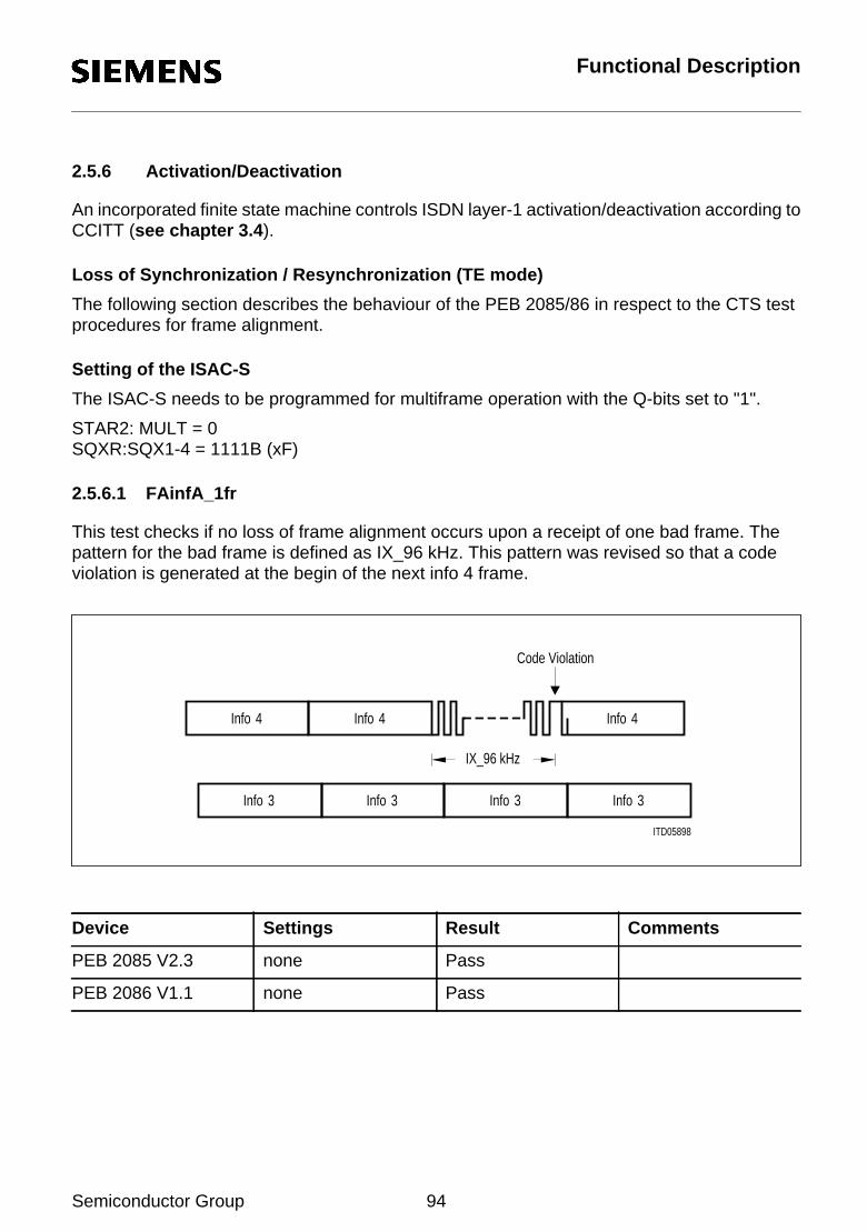
Functional Description
2.5.6 Activation/Deactivation
An incorporated finite state machine controls ISDN layer-1 activation/deactivation according toCCITT (see chapter 3.4 ).
Loss of Synchronization / Resynchronization (TE mode)
The following section describes the behaviour of the PEB 2085/86 in respect to the CTS testprocedures for frame alignment.
Setting of the ISAC-S
The ISAC-S needs to be programmed for multiframe operation with the Q-bits set to "1".
STAR2: MULT = 0SQXR:SQX1-4 = 1111B (xF)
2.5.6.1 FAinfA_1fr
This test checks if no loss of frame alignment occurs upon a receipt of one bad frame. Thepattern for the bad frame is defined as IX_96 kHz. This pattern was revised so that a codeviolation is generated at the begin of the next info 4 frame.
Device Settings Result Comments
PEB 2085 V2.3 none Pass
PEB 2086 V1.1 none Pass
ITD05898
Info 4
Info 3 3Info
4Info
Info 3
IX_96 kHz
3Info
Info 4
Code Violation
Semiconductor Group 94

Functional Description
2.5.6.2 FAinfB_1fr
This test uses a frame which has no framing and balancing bit.
2.5.6.3 FAinfD_1fr
This test uses a frame which remains at binary "1" until the first code violation in bit 16. Sinceit is specified, that a terminal should mirror the received FA-bit in the transmitted FA-bit, a frameis generated by the IUT which will not generate a second code violation. The pattern for acorrect i3_BASIC frame states that the FA-bit may have any value.
Device Settings Result Comments
PEB 2085 V2.3 none Pass
PEB 2086 V1.1 none Pass
Device Settings Result Comments
PEB 2085 V2.3 none Pass
PEB 2086 V1.1 none Pass
ITD05899
Info 4
Info 3 3Info
4Info
Info 3
I4_BASIC IX_I4noflag
3Info
Info 4
Code Violation
ITD05900
Info 4
Info 3 3Info
4Info
Info 3 with
Info 3
Info 4
AF 1=
AF 1=
Semiconductor Group 95

Functional Description
2.5.6.4 FAinfA_kfr
This test uses a number of IX_96 kHz frames to check the loss of synchronization.
2.5.6.5 FAinfB_kfr
This test uses a number of IX_I4noflag frames to check the loss of synchronization.
Device Settings Result Comments
PEB 2085 V2.3 n = 2 Pass
PEB 2086 V1.1 n = 2 Pass
Device Settings Result Comments
PEB 2085 V2.3 n = 2 Pass
PEB 2086 V1.1 n = 2 Pass
ITD05901
Info 4
Info 3 3Info
4Info
Info 3
IX_96
I3_SFAL 0Info
kHz kHzIX_96 kHzIX_96
ITD05902
Info 4
Info 3 3Info
4Info
Info 3
I4_BASIC IX_I4noflag IX_I4noflag IX_I4noflag
I3_SFAL 0Info
Semiconductor Group 96
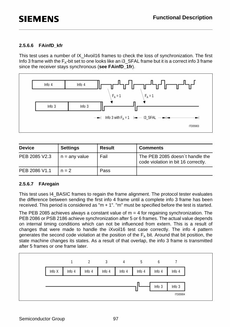
Functional Description
2.5.6.6 FAinfD_kfr
This test uses a number of IX_I4voil16 frames to check the loss of synchronization. The firstInfo 3 frame with the FA-bit set to one looks like an i3_SFAL frame but it is a correct info 3 framesince the receiver stays synchronous (see FAinfD_1fr ).
2.5.6.7 FAregain
This test uses I4_BASIC frames to regain the frame alignment. The protocol tester evaluatesthe difference between sending the first info 4 frame until a complete info 3 frame has beenreceived. This period is considered as "m + 1". "m" must be specified before the test is started.
The PEB 2085 achieves always a constant value of m = 4 for regaining synchronization. ThePEB 2086 or PSB 2186 achieve synchronization after 5 or 6 frames. The actual value dependson internal timing conditions which can not be influenced from extern. This is a result ofchanges that were made to handle the iXvoil16 test case correctly. The info 4 patterngenerates the second code violation at the position of the FA bit. Around that bit position, thestate machine changes its states. As a result of that overlap, the info 3 frame is transmittedafter 5 frames or one frame later.
Device Settings Result Comments
PEB 2085 V2.3 n = any value Fail The PEB 2085 doesn´t handle thecode violation in bit 16 correctly.
PEB 2086 V1.1 n = 2 Pass
ITD05903
Info 4
Info 3 3Info
4Info
I3_SFAL
AF 1=
with3Info
F =A 1
F =A 1
ITD05904
Info X 4Info
1 2
Info 4
3
Info 4
4
Info 4
5
Info 4
6
Info 4
7
Info 4
3InfoInfo 3
Semiconductor Group 97
Functional Description
2.5.7 D-Channel Access
Depending on the application, the D channel is either switched transparently (no collisionresolution) from the IOM to the S/T interface (LT-S and NT modes) or it is submitted to the D-channel access procedure according to CCITT recommendation I.430 (TE mode). For trunkline applications (LT-T mode) both modes of D-channel processing are applicable and may beselected by appropriate register programming of the ISAC-S.
The D-channel access procedure according to CCITT I.430 including priority management isfully implemented in the ISAC-S:
In TE and LT-T mode, if collision detection is programmed (MODE:DIM2-0), a collision isdetected if either an echo bit of "0" is recognized and a D bit of "1" was generated, or an echobit of "1" is recognized and a D bit of "0" was generated. When this occurs, D-channeltransmission is immediately stopped, and the echo channel is monitored to enable asubsequent D-channel access to be attempted.
When used in LT-S (NT) mode the device generates the echo bits necessary for D-channelcollision detection.
Stop/Go Bit
As the collision resolution is performed by the layer-1 part of the device, an information aboutthe D-channel status ("ready" or "busy") must be sent back to the layer-2 part to control HDLCtransmission. For this goal a Stop/Go (S/G) bit is transmitted over the IOM interface to thelayer-2 device.
Depending on the selected IOM mode the S/G bit is either transmitted in bit 20 of an IOM-1frame (4-byte frame structure) or in bit 90 of an IOM-2 frame (12-byte structure) (seefigures 26 and 40).
A logical "1" of the S/G bit indicates a collision on the S bus. By sending the S/G bit a logical"0" to the layer-2 controller in anticipation of the S bus D channel "ready"-state, the first valid0 bits will emerge from the layer-1 part at exactly that moment an access is becoming possible.
Selection of D-Channel Access Mode
For proper operation of the D-channel access procedure, the ISAC-S must be programmed via the MODE (see chapter 4.1.7) register to evaluate the Stop/Go bit. This is achieved by setting
Device Settings Result Comments
PEB 2085 V2.3 m = 4 Fail
PEB 2086 V1.1 m = 5 or 6 Pass
Semiconductor Group 98

Functional Description
MODE:DIM2-0 to 001 or 011.
Selection of the Priority Class
The priority class (priority 8 or priority 10) is selected by transferring the appropriate activationcommand via the Command/Indicate (C/I) channel of the IOM interface to the layer-1controller. If the activation of the S interface is initiated by a TE, the priority class is selectedimplicitly by the choice of the activation command. If the S interface is activated from the NT,an activation command selecting the desired priority class should be programmed at the TEon reception of the activation indication (AI8). In the activated state, the priority class may bechanged whenever required simply by programming the respective activation requestcommand (AR8 or AR10). The following table summarizes the C/I codes used for setting thepriority classes:
Table 6Priority Commands/Indications for TE/LT-T Mode
Command (upstream)
Activate request, set priority 8
Remarks
Activation command: Set D-channelpriority to 8
Abbr.
AR8
Code
1000
Activate request, set priority 10 Activation command: Set D-channelpriority to 10
AR10 1001
Indication (downstream)
Activate indication with priorityclass 8
Remarks
Info 4 received: D-channel priority is 8or 9
Abbr.
AI8
Code
1100
Activate indication with priorityclass 10
Info 4 received: D-channel priority is10 or 11
AI10 1101
Semiconductor Group 99

Functional Description
2.5.8 S- and Q-Channel Access
Access to the received/transmitted S or Q channel is provided via registers. As specified byCCITT I.430, the Q bit is transmitted from TE to NT in the position normally occupied by theauxiliary framing bit (FA) in one frame out of 5, whereas the S bit is transmitted from NT to TEin a spare bit, see figure 43.
The functions provided by the ISAC-S are:
TE/LT-T mode:
– Synchronization to the received 20-frame multiframe by means of the received M bit pattern.Synchronism is achieved when the M bit has been correctly received during 20 consecutiveframes starting from frame number 1 (table 7).
– When synchronism is achieved, the four received S bits in frames 1, 6, 11 and 16 are storedas SQR1 to SQR4 in the SQRR register if the complete M bit multiframe pattern wascorrectly received in the corresponding multiframe. A change in any of the received four bits(SQR1, 2, 3 or 4) is indicated by an interrupt (CISQ in ISTA and SQC in CIR0).
– When an M bit is observed to have a value different from that expected, the synchronism isconsidered lost. The SQR bits are not updated until synchronism is regained. Thesynchronization state is constantly indicated by the SYN bit in the SQRR register.
– When synchronism with the received multiframe is achieved, the four bits SQX1 to SQX4stored in the SQXR register are transmitted as the four Q bits (FA bit position) in frames 1,6, 11 and 16 respectively (starting from frame number one). Otherwise the bit transmitted isa mirror of the received FA bit. At loss of synchronism (mismatch in M bit) the mirroring isresumed starting with the next FA bit.
Semiconductor Group 100

Functional Description
LT-S/NT mode:
– Generation of the FA and M bit patterns according to table 7.
– The four bits received in the FA bit position in frames 1, 6, 11 and 16 (Q bits) are stored asSQR1 to SQR4 in the SQRR register. A change in any of the received bits (SQR1 or 2 or 3or 4) is indicated by interrupt (CISQ in ISTA).
– The four bits SQX1 to SQX4 stored in the SQXR register are transmitted as the four S bitsin frames 1, 6, 11 and 16, respectively.
– The S/T multiframe generation can be disabled in the STAR2 register (MULT bit).
Table 7S and Q Bit Position Identification and Multiframe Structure
S and Q Channel Structure
Frame Number
1 2 3 4 5
NT-to-TEFA bitPosition
ONEZEROZEROZEROZERO
NT-to-TEM Bit
ONEZEROZEROZEROZERO
NT-to-TES Bit
S1ZEROZEROZEROZERO
TE-to-NTFA bitPosition
Q1ZEROZEROZEROZERO
6 7 8 910
ONEZEROZEROZEROZERO
ZEROZEROZEROZEROZERO
S2ZEROZEROZEROZERO
Q2ZEROZEROZEROZERO
1112131415
ONEZEROZEROZEROZERO
ZEROZEROZEROZEROZERO
S3ZEROZEROZEROZERO
Q3ZEROZEROZEROZERO
1617181920
ONEZEROZEROZEROZERO
ZEROZEROZEROZEROZERO
S4ZEROZEROZEROZERO
Q4ZEROZEROZEROZERO
1 2etc.
ONEZERO
ONEZERO
S1ZERO
Q1ZERO
Semiconductor Group 101

Functional Description
2.5.9 S-Frame and Multiframe Synchronization (PEB 2086 only)
The PEB 2086 offers the capability to control the start of the S-frame as well as the start of themultiframe from external signals. Applications which require synchronization between differentS-interfaces are possible. Such an application is the connection of DECT base stations to PBXline cards.
Figure 54Multiframe Synchronization using the M-Bit
2.5.9.1 S-Frame Start (LT-S, NT mode)
The CP-input can be used as S-frame trigger. Therefore, a 4 kHz signal must be applied.
If no signal is applied (CP = 0) the S-frames are triggerd internally.
2.5.9.2 Multiframe / Superframe Synchronization (LT-S, NT-Mode)
The X2 pin can be used to synchronize the multiframe structure between severalS-transceivers. Multiframe generation must be enabled.
The value of X2 is sampled at the falling edge of CP or at the start of the F-bit of the S-framewhatever occurs earlier.
If the input on X2 is "1", the multiframe counter is reset to frame no.1 and as a result, the M-bitis transmitted as "1".
ITS03735
PEB 2086 CP
X2X2
PEB 2086
S-Interface
4 kHz
M-BitM-Bit LT-S,NTTE
RISAC -S -SISAC R
Semiconductor Group 102

Functional Description
If X2 become "0" again, the multiframe counter counts 20 frames and begins againautonomously.
If X2 is kept "1", the multiframe counter is permanently reset and the M-bit stays at "1". If X2becomes "0" for only one S-frame, the multiframe-counter reaches frame no. 2 at which "0" istransmitted in the M-bit location.
Thus, the M-bit can be use to transfer synchronization pulses of any internal between differentS-interfaces.
Figure 55S-Frame Trigger and Multiframe Generation
2.5.9.3 M-Bit Output (TE Mode)
In TE mode, the PEB 2086 outputs the value of the M-bit multiplexed to the value of the Echo-bits on the X2 pin.
The value of M should be sampled at the falling edge of FSC.
ITS05897
CPSFS
S U
Multi-Frame
Reset
SSYNCX2
Counter
S-FrameGenerator Transmitter
Semiconductor Group 103

Functional Description
2.6 Terminal Specific Functions
Watchdog and External Awake
In addition to the ISAC-S standard functions supporting the ISDN basic access, the ISAC-Scontains optional functions, useful in various terminal configurations.
The terminal specific functions are enabled by setting bit TSF (STCR register) to "1". This hastwo effects:
– The SIP/EAW line is defined as an External Awake input (and not as SLD line);
– Second, the interrupts SAW and WOV (EXIR register) are enabled:
SAW (Subscriber Awake) generated by a falling edge on the EAW line
WOV (Watchdog timer overflow) generated by the watchdog timer. This occurs when theprocessor fails to write two consecutive bit patterns in ADF1:
The WTC1 and WTC2 bits have to be successively written in the following manner within128 ms:
As a result the watchdog timer is reset and restarted. Otherwise a WOV is generated.
Deactivating the terminal specific functions is only possible with a hardware reset.
Having enabled the terminal specific functions via TSF=1, the user can make the ISAC-Sgenerate a reset signal by programming the Reset Source Select RSS bit (CIXR/CIX0register), as follows:
0 → A reset signal is generated as a result of
– a falling edge on the EAW line (subscriber awake)
– a C/I code change (exchange awake)
A falling edge on the EAW line also forces the IDP1 line of the IOM interface to zero.The consequence of this is that the IOM interface and the ISAC-S leaves thepower-down state.
A corresponding interrupt status (CISQ or SAW) is also generated.
ADF1 WTC2WTC1
Watchdog Timer Control 1, 0.
WTC1 WTC2
10
1.2.
01
Semiconductor Group 104

Functional Description
1 → A reset signal is generated as a result of the expiration of the watchdog timer(indicated by the WOV interrupt status).
Note that the watchdog timer is not running when the ISAC-S is in the power-downstate (IOM not clocked).
Note: Bit RSS has a significance only if terminal specific functions are activated (TSF=1).
The RSS bit should be set to "1" by the user when the ISAC-S is in power-up to prevent anedge on the EAW line or a change in the C/I code from generating a reset pulse.
Switching RSS from 0 to 1 or from 1 to 0 resets the watchdog timer.
The reset pulse generated by the ISAC-S (output via RST pin) has a pulse width of:– 125 µs when generated by the watchdog timer– 16 ms when generated by EAW line or C/I code change.
Semiconductor Group 105

Functional Description
2.7 Test Functions
The ISAC-S provides several test and diagnostic functions which can be grouped as follows: digital loop via TLP (Test Loop, SPCR register) command bit: IDP1 is internally connected
with IDP0, output from layer 1 (S/T) on IDP0 is ignored; this is used for testing ISAC-Sfunctionality excluding layer 1;
test of layer-2 functions while disabling all layer-1 functions and pins associated with them(including clocking, in TE mode), via bit TEM (Test Mode in ADF1 register); the ISAC-S isthen fully compatible to the ICC (PEB 2070) seen at the IOM interface. Note that in IOM-1mode also the internal pull-up resistors at IDP0/1 are disconnected.
loop at the analog end of the S interface;
TE/LT-T:
Test loop 3 is activated with the C/I channel command Activate Request Loop (ARL). An Sinterface is not required since INFO3 is looped back to the receiver. When the receiver hassynchronized itself to this signal, the message "Test Indication" (or "Awake Test Indication") isdelivered in the C/I channel. No signal is transmitted over the S interface.
In the test loop mode the S interface awake detector is enabled i.e. if a level is detected (e.g.Info 2/Info 4) this will be reported by the Awake Test Indication (ATI). The loop function is noteffected by this condition and the internally generated 192-kHz line clock does not depend onthe signal received at the S interface.
NT/LT-S:
Test loop 2 is likewise activated over the IOM interface with Activate Request Loop (ARL). NoS line is required. INFO4 is looped back to the receiver and also sent to the S interface. Whenthe receiver is synchronized, the message "AIU" is sent in the C/I channel. In the test loopmode the S interface awake detector is disabled, and echo bits are set to logical "0".
special loops are programmed via C2C1-0 and C1C1-0 bits (register SPCR) transmission of special test signals on the S/T interface according to the modified AMI code
are initiated via a C/I command written in CIXR/CIX0 register (cf. chapter 3.4).
Two kinds of test signals may be sent by the ISAC-S: single pulses and continuous pulses.
The single pulses are of alternating polarity, one S interface bit period wide, 0.25 ms apart, witha repetition frequency of 2 kHz. Single pulses can be sent in all applications. Thecorresponding C/I command in TE, LT-S and LT-T applications is SSZ (Send single zeros).Alternatively, this test mode can be effected by pulling pin SSZ (pin X2, NT mode only) tological "0".
Continuous pulses are likewise of alternating polarity, one S-interface bit period wide, but theyare sent continuously. The repetition frequency is 96 kHz. Continuous pulses may betransmitted in all applications. This test mode is entered in LT-S, LT-T and TE applications withthe C/I command SCZ. Alternatively, pin SCZ (pin CP, NT mode only) can be pulled to logical"0".
Semiconductor Group 106

Functional Description
2.8 Layer-2 Functions for the ISDN Basic Access
LAPD, layer 2 of the D-channel protocol (CCITT I.441) includes functions for:
– Provision of one or more data link connections on a D channel (multiple LAP).Discrimination between the data link connections is performed by means of a data linkconnection identifier (DLCI = SAPI + TEI)
– HDLC-framing
– Application of a balanced class of procedure in point-multipoint configuration.
The simplified block diagram in figure 56 shows the functional blocks of the ISAC-S whichsupport the LAPD protocol.
Figure 56D-Channel Processing of the ISAC®-S
ITS00861
StatusCommandRegisters
ControllerLAPDHDLC
TransmitterReceiverHDLC
R-FIFO X-FIFO FIFOController2 x 32 byte
P-Interfaceµ
µC-System
Layer-1Functions
S(D-Channel)
Layer 1
2Layer
LayersUpper
RIOM
2 x 32 byte
Semiconductor Group 107

Functional Description
For the support of LAPD the ISAC-S contains an HDLC transceiver which is responsible forflag generation/recognition, bit stuffing mechanism, CRC check and address recognition.
A powerful FIFO structure with two 64-byte pools for transmit and receive directions and anintelligent FIFO controller permit flexible transfer of protocol data units to and from the µCsystem.
2.8.1 Message Transfer Modes
The HDLC controller can be programmed to operate in various modes, which are different inthe treatment of the HDLC frame in the receive direction. Thus, the receive data flow and theaddress recognition features can be programmed in a flexible way, which satisfies differentsystem requirements.
In the auto mode the ISAC-S handles elements of procedure of the LAPD (S and I frames)according to CCITT I.441 fully autonomously.
For the address recognition the ISAC-S contains four programmable registers for individualSAPI and TEI values SAP1-2 and TEI1-2, plus two fixed values for "group" SAPI and TEI,SAPG and TEIG.
There are 5 different operating modes which can be set via the MODE register (addr. 22H):
Auto mode (MDS2, MDS1 = 00)
Characteristics:
– Full address recognition (1 or 2 bytes).
– Normal (mod 8) or extended (mod 128) control field format
– Automatic processing of numbered frames of an HDLC procedure
If a 2-byte address field is selected, the high address byte is compared with the fixed valueFEH or FCH (group address) as well as with two individually programmable values in SAP1and SAP2 registers. According to the ISDN LAPD protocol, bit 1 of the high byte address willbe interpreted as command/response bit (C/R) dependent on the setting of the CRI bit inSAP1, and will be excluded from the address comparison.
Similarly, the low address byte is compared with the fixed value FFH (group TEI) and twocompare values programmed in special registers (TEI1, TEI2). A valid address will berecognized in case the high and low byte of the address field match one of the compare values.The ISAC-S can be called (addressed) with the following address combinations:
– SAP1/TEI1
– SAP1/FFH
– SAP2/TEI2
– SAP2/FFH
– FEH (FCH)/TEI1
– FEH (FCH)/TEI2
– FEH (FCH)/FFH
Semiconductor Group 108

Functional Description
Only the logical connection identified through the address combination SAP1, TEI1 will beprocessed in the auto mode, all others are handled as in the non-auto mode. The logicalconnection handled in the auto mode must have a window size 1 between transmitted andacknowledged frames. HDLC frames with address fields that do not match with any of theaddress combinations, are ignored by the ISAC-S.
In case of a 1-byte address, TEI1 and TEI2 will be used as compare registers. According tothe X.25 LAPB protocol, the value in TEI1 will be interpreted as command and the value inTEI2 as response.
The control field is stored in the RHCR register and the I field in the RFIFO. Additionalinformation is available in the RSTA.
Non-auto mode (MDS2, MDS1 = 01)
Characteristics: Full address recognition (1 or 2 bytes)Arbitrary window sizes
All frames with valid addresses (address recognition identical to auto mode) are accepted andthe bytes following the address are transferred to the µP via RHCR and RFIFO. Additionalinformation is available in the RSTA.
Transparent mode 1 (MDS2, MDS1, MDS0 = 101)
Characteristics: TEI recognition
A comparison is performed only on the second byte after the opening flag, with TEI1, TEI2 andgroup TEI (FFH). In the case of a match, the first address byte is stored in SAPR, the (first byteof the) control field in RHCR, and the rest of the frame in the RFIFO. Additional information isavailable in the RSTA.
Transparent mode 2 (MDS2, MDS1, MDS0 = 110)
Characteristics: no address recognition
Every received frame is stored in the RFIFO (first byte after opening flag to CRC field).Additional information can be read from the RSTA.
Transparent mode 3 (MDS2, MDS1, MDS0 = 111)
Characteristics: SAPI recognition
A comparison is performed on the first byte after the opening flag with SAP1, SAP2 and groupSAPI (FE/FCH). In the case of a match, all the following bytes are stored in RFIFO. Additionalinformation can be read from the RSTA.
2.8.2 Protocol Operations (auto mode)
In addition to address recognition all S and I frames are processed in hardware in the automode. The following functions are performed:
– update of transmit and receive counter
– evaluation of transmit and receive counter
Semiconductor Group 109

Functional Description
– processing of S commands
– flow control with RR/RNR
– response generation
– recognition of protocol errors
– transmission of S commands, if an acknowledgement is not received
– continuous status query of remote station after RNR has been received
– programmable timer/repeater functions.
The processing of frames in auto mode is described in detail in chapter 2.8.5: Documentationof the Auto Mode.
2.8.3 Reception of Frames
A 2 × 32 byte FIFO buffer (receive pools) is provided in the receive direction.
The control of the data transfer between the CPU and the ISAC-S is handled via interrupts.
There are two different interrupt indications concerned with the reception of data:
– RPF (Receive Pool Full) interrupt, indicating that a 32-byte block of data can be read fromthe RFIFO and the received message is not yet complete.
– RME (Receive Message End) interrupt, indicating that the reception of one message iscompleted, i.e. either
one message ≤ 32 bytes, or
the last part of a message > 32 bytes
is stored in the RFIFO.
Depending on the message transfer mode the address and control fields of received framesare processed and stored in the Receive FIFO or in special registers as depicted in figure 58.
The organization of the RFIFO is such that up to two short (≤ 32 bytes), successive messages,with all additional information can be stored. The contents of the RFIFO would be, for example,as shown in figure 57.
Semiconductor Group 110

Functional Description
Figure 57Contents of RFIFO (short message)
ITS01502
31
31
0
0
ReceiveMessage 2
bytes)321Message
Receive
RME
RME
Interrupts inWait Line
RFIFO
(_<
bytes)_<( 32
Semiconductor Group 111

Functional Description
Figure 58Receive Data Flow
Note 1 Only if a 2-byte address field is defined (MDS0 = 1 in MODE register).
Note 2 Comparison with Group TEI (FFH) is only made if a 2-byte address field is defined(MDS0 = 1 in MODE register).
Note 3 In the case of an extended, modulo 128 control field format (MCS = 1 in SAP2 register)the control field is stored in the RHCR in compressed form (I frames).
Note 4 In the case of extended control field, only the first byte is stored in the RHCR, thesecond in the RFIFO.
ITD02342
Description of Symbols:
Checked automatically by
Compared with Register or Fixed Value
Stored Info Register or RFIFO
Flag HighAddress Address
Low Control Information CRC Flag
RSTARHCRFFTEI1, TEI2SAP1, SAP2
FE, FC
(Note 1) 2)(Note (Note 3)
RFIFO
RFIFOFE, FCSAP1, SAP2 TEI1, TEI2
FF RHCR RSTA
4)(Note (Note 2)1)(Note
RSTARHCRFFTEI1, TEI2 RFIFO
RSTA
SAPR
RSTA
RFIFO
RFIFOSAP1, SAP2FE, FC
Auto Mode(U and Frames)Ι
Non-AutoMode
ModeTransparent
1
2TransparentMode
3TransparentMode
-- -
(Note 4)
RISAC -S
Semiconductor Group 112

Functional Description
When 32 bytes of a message longer than that are stored in the RFIFO, the CPU is promptedto read out the data by an RPF interrupt. The CPU must handle this interrupt before more than32 additional bytes are received, which would cause a "data overflow" (figure 59).Thiscorresponds to a maximum CPU reaction time of 16 ms (data rate 16 kbit/s).After a remaining block of less than or equal to 16 bytes has been stored, it is possible to storethe first 16 bytes of a new message (see figure 59).The internal memory is now full. The arrival of additional bytes will result in "data overflow"(RSTA:RDO) and a third new message in "frame overflow" (EXIR:RFO).The generated interrupts are inserted together with all additional information into a queue tobe individually passed to the CPU.
After an RPF or RME interrupt has been processed, i.e. the received data has been read fromthe RFIFO, this must be explicitly acknowledged by the CPU issuing an RMC (ReceiveMessage Complete) command.
The ISAC-S can then release the associated FIFO pool for new data. If there is an additionalinterrupt in the queue it will be generated after the RMC acknowledgement.
Figure 59Contents of the RFIFO (long messages)
ITS01501
31
31
0
0
Message 2
1MessageLong
RPF
RME
Interrupts inthe Queue
RFIFORFIFOthe Queue
Interrupts in
RPF
RPF
LongMessage
0
0
31
31
1516
RME
bytes)46<(_
bytes)32<(_
Semiconductor Group 113

Functional Description
Information about the received frame is available for the µP when a RME interrupt is generated,as shown in table 8.
Table 8Receive Information at RME Interrupt
2.8.4 Transmission of Frames
A 2 × 32 byte FIFO buffer (transmit pools) is provided in the transmit direction.
If the transmit pool is ready (which is true after an XPR interrupt or if the XFW bit in STAR is
Information
Recognition of TEI
Mode
All except transparent modes 2, 3RSTA (27) TA
First byte after flag(SAPI of LAPDaddress field)
Transparent mode 1SAPR (26) –
Control field Auto mode, I (modulo 8) and U framesRHCR (29) –
Compressed control field Auto mode, I frames (modulo 128)RHCR (29) –
Type of frame(Command/Response)
Auto mode, 2 byte address fieldNon-auto mode, 2-byte address fieldTransparent mode 3
RSTA (27) C/R
2nd byte after flag Non-auto mode, 1-byte address fieldRHCR (29) –
3rd byte after flag Non-auto mode, 2-byte address fieldTransparent mode 1
RHCR (29) –
Recognition of SAPI Auto mode, 2 byte address fieldNon-auto mode, 2-byte address fieldTransparent mode 3
RSTA (27) SA1-0
Result of CRC check(correct/incorrect)
ALLRSTA (27) CRC
Data available in RFIFO(yes/no)
ALLRSTA (27) RDA
Abort condition detected(yes/no)
ALLRSTA (27) RAB
Number of bytes receivedin RFIFO
ALLRBCL (25) RBC4-0
Message length ALLRBCL RBCH
(25)(2A)
RBC11-0OV
Data overflow duringreception of a frame(yes/no)
ALLRSTA (27) RDO
Register (adr.hex)
Bit
Semiconductor Group 114

Functional Description
set), the CPU can write a data block of up to 32 bytes to the transmit FIFO. After this, datatransmission can be initiated by command.
Two different frames types can be transmitted:
– Transparent frame (command: XTF), or
– I frames (command: XIF)
as shown in figure 60.
For transparent frames, the whole frame including address and control field must be written tothe XFIFO.
Figure 60Transmitter Data Flow
The transmission of I frames is possible only if the ISAC-S is operating in the auto-mode. Theaddress and control field is autonomously generated by the ISAC-S and appended to theframe, only the data in the information field must be written to the XFIFO.
If a 2 byte address field has been selected, the ISAC-S takes the contents of the XAD 1 registerto build the high byte of the address field, and the contents of the XAD 2 register to build thelow byte of the address field.
Additionally the C/R bit (bit 1 of the high byte address, as defined by LAPD protocol) is set to"1" or "0" dependent on whether the frame is a command or a response.
ITD02341
Flag Address Control Information CRC Flag
FlagCRCXFIFOControlXAD1Flag
HDLC Frame
Flag XAD1 Control XFIFO CRC Flag
FlagCRCXFIFOFlag
XAD2
(XIF)Transmit I-Frame
Auto Mode, 8-Bit Addr.
16-Bit Addr.Auto Mode,
Transmit I-Frame(XIF)
All Modes
Transmit TransparentFrame (XTF)
Note: Length of Control Field is b or 16
Description of Symbols:
Bit
Generated automatically by
Written initially by CPU
Loaded (repeatedly)
(Info Register)
by CPU upon(XPR Interrupt)request
-
RISAC -S
RISAC -S
Semiconductor Group 115

Functional Description
In the case of a 1 byte address, the ISAC-S takes either the XAD 1 or XAD 2 register todifferentiate between command or response frame (as defined by X.25 LAP B).
The control field is also generated by the ISAC-S including the receive and send sequencenumber and the poll/final (P/F) bit. For this purpose, the ISAC-S internally manages send andreceive sequence number counters.
In the auto mode, S frames are sent autonomously by the ISAC-S. The transmission of Uframes, however, must be done by the CPU. U frames must be sent as transparent frames(CMDR:XTF), i.e. address and control field must be defined by the CPU.
Once the data transmission has been initiated by command (CMDR:XTF or XIF), the datatransfer between CPU and the ISAC-S is controlled by interrupts.
The ISAC-S repeatedly requests another data packet or block by means of an ISTA:XPRinterrupt, every time no more than 32 bytes are stored in the XFIFO.
The processor can then write further data to the XFIFO and enable the continuation of frametransmission by issuing an XIF/XTF command.
If the data block which has been written last to the XFIFO completes the current frame, thismust be indicated additionally by setting the XME (Transmit Message End) command bit. TheISAC-S then terminates the frame properly by appending the CRC and closing flag.
If the CPU fails to respond to an XPR interrupt within the given reaction time, a data underruncondition occurs (XFIFO holds no further valid data). In this case, the ISAC-S automaticallyaborts the current frame by sending seven consecutive "ones" (ABORT sequence).
The CPU is informed about this via an XDU (Transmit Data Underrun) interrupt.
It is also possible to abort a message by software by issuing a CMDR:XRES (TransmitterRESet) command, which causes an XPR interrupt.
After an end of message indication from the CPU (CMDR:XME command), the termination ofthe transmission operation is indicated differently, depending on the selected messagetransfer mode and the transmitted frame type.
If the ISAC-S is operating in the auto mode, the window size (= number of outstandingunacknowledged frames) is limited to "1"; therefore an acknowledgement is expected for everyI frame sent with an XIF command. The acknowledgement may be provided either by areceived S or I frame with corresponding receive sequence number.
If no acknowledgement is received within a certain time (programmable), the ISAC-S requestsan acknowledgement by sending an S frame with the poll bit set (P = 1) (RR or RNR). If noresponse is received again, this process is repeated in total N2 times (retry count,programmable via TIMR register).
Semiconductor Group 116

Functional Description
The termination of the transmission operation may be indicated either with:
– XPR interrupt, if a positive acknowledgement has been received,
– XMR interrupt, if a negative acknowledgement has been received, i.e. the transmittedmessage must be repeated (XMR = Transmit Message Repeat),
– TIN interrupt, if no acknowledgement has been received at all after N2 times the expirationof the time period t1 (TIN = Timer INterrupt, XPR interrupt is issued additionally).
Note: Prerequisite for sending I frames in the auto mode (XIF) is that the internal operationalmode of the timer has been selected in the MODE register (TMD bit = 1).
The transparent transmission of frames (XTF command) is possible in all message transfermodes. The successful termination of a transparent transmission is indicated by an XPRinterrupt.
In all cases, collisions which occur on the S-bus (D channel) before the first XFIFO pool hasbeen completely transmitted and released are treated without µP interaction. The ISAC-S willretransmit the frame automatically.
If a collision is detected after the first pool has been released, the ISAC-S aborts the frame andrequests the processor to repeat the frame with an XMR interrupt.
2.8.5 Documentation of the Auto Mode
The auto mode of the ICC and ISAC-S is only applicable for the states 7 and 8 of the LAPDprotocol. All other states (1 to 6) have to be performed in Non-Auto Mode (NAM). Thereforethis documentation gives an overview of how the device reacts in the states 7 and 8, whichreactions require software programming and which are done by the hardware itself, wheninterrupts and status register contents are set or change. The necessary software actions arealso detailed in terms of command or mode register access.
The description is based on the SDL-diagrams of the ETSI TS 46-20 dated 1989.
The diagrams are only annotated by documentary signs or texts (mostly register descriptions)and can therefore easily be interpreted by anyone familiar with the SDL description of LAPD.All deviations that occur are specially marked and the impossible actions, paths etc. arecrossed out.
To get acquainted with this documentation, first read through the legend-description and theadditional general considerations, then start with the diagrams, referring to the legend and theregister description in the Technical Manual if necessary.
We hope you will profit from this documentation and use our software-saving auto mode.
Semiconductor Group 117

Functional Description
2.8.5.1 Legend of the Auto-Mode-Documentation
a. Symbols within a path
There are 3 symbols within a path
a.1.
a.2.
a.3.
In the auto mode the device processes all subsequent state transitionsbranchings etc. up to the next symbol.
In the auto mode the device does not process the state transitions,branchings etc. Within the path appropriate directions are given withwhich the software can accomplish the required action.
A path cannot be implemented and no software or hardware actioncan change this. These paths are either optional or only applicable forwindow-size > 1.
Semiconductor Group 118
Functional Description
b. Symbols at a path
There is 1 symbol at a path
b.1.
c. Symbols at an internal or external message box.
There are 2 symbols at a message box.
c.1.
Note: The impossibility to perform the optional T203 timer-procedure is not explicitly men-tioned; the corresponding actions are only crossed out.
c.2.
d. Text within boxes
Text within boxes can be grouped in one of two classes.
d.1.
d.2. The text describes a register access
The text is placed in the box that describes the functions for which the register access isneeded.
marks the beginning of a path, for which a.3 applies.
This symbol means, that the action described in the box is notpossible. Either the action specified is not done at all or an additionalaction is taken (written into the box).
Box
This symbol means, that within a software-path, by taking theprescribed register actions the contents of the box will be doneautomatically.
Box
The text denotes an interrupt which is always associated with theevent. (But can also be associated with other events). (See ISTA andEXIR register description in the Technical Manual for an interruptdescription).
Text
Text
BoxBox or
either a register read access to discriminate this state from others orto reach a branching condition
or a register write access to give a command.Text
Box
Semiconductor Group 119
Functional Description
e. Text attached at the side of boxes
e.1.
e.2.
(The attached texts can also be placed on the left side.)
f. Text above and below boxes
f.1.
f.2.
g. Shade boxes
The text describes an Interrupt associated with the contents of thebox. The interrupt is always associated with the box contents, if theinterrupt name is not followed by a "/", it is associated only underappropriate conditions if a "/" is behind it.
TextBox
The text describes a possible or mandatory change of a bit in a status-register associated with the contents of the box.
Text
Box
Text describes a mandatory action to be performed on the contents ofthe box.
Text
Box
Text describes a mandatory action to be taken as a result of thecontents of the box.Action here means register access.Text
Box
The box describes an impossible state or action for the device.
Box
Semiconductor Group 120
Functional Description
2.8.5.2 Additional General Considerations when Using the Auto Mode
a) Switching from auto mode to non-auto mode.
As mentioned in the introduction the auto mode is only applicable in the states 7 and 8 ofthe LAPD. Therefore whenever these states have to be left (which is indicated by a"Mode:NAM" text) there are several actions to be taken that could not all be detailed in theSDL-diagrams:
a.1) write non-auto mode and TMD = 0 into the mode register.
a.2) write the timer register with an arbitrary value to stop it. The timer T200 as specifiedin the LAPD-protocol is implemented in the hardware only in the states 7 and 8; in allother states this or any other timer-procedure has to be done by the software with thepossible use of the timer in external timer mode.
a.3) read the WFA bit of the STAR2 register and store it in a software variable. Theinformation in this bit may be necessary for later decisions. When switching from automode to non-auto mode XPR interrupts may be lost.
a.4) In the non-auto mode the software has to decode I, U and S-frames because I and Sframes are only handled autonomously in the auto mode.
a.5) The RSC and PCE interrupts, the contents of the STAR2 register and the RRNR bitin the STAR register are only meaningful within the auto mode.
a.6) leave some time before RHR or XRES is written to reset the counters, as a currentlysent frame may not be finished yet.
b) What has to be written to the XFIFO?
In the legend description when the software has to write contents of a frame to the XFIFOonly "XFIFO" is shown in the corresponding box. We shall give here a general rule of whathas to be written to the XFIFO:
a) For sending an I-frame with CMDR:XIF, only the information field content, i.e. no SAPI,TEI, Control field should be written to the XFIFO.
b) For sending an U-frame or any other frame with CMDR:XTF, the SAPI, TEI and thecontrol field has to be written to the XFIFO.
c) The interrupts XPR and XMR.
The occurence of an XPR interrupt in auto mode after an XIF command indicates that theI-frame sent was acknowledged and the next I frame can be sent, if STAR2:TRECindicates state 7 and STAR:RRNR indicates Peer Rec not busy. If Peer Rec is busy afteran XPR, the software should wait for the next RSC interrupt before sending the next I-frame. If the XPR happens to be in the timer recovery state, the software has to poll theSTAR2 register until the state multiple frame established is reached or a TIN interrupt isissued which requires auto mode to be left (One of these two conditions will occur beforethe time T200*N200). In non-auto mode or after an XTF command the XPR just indicates,that the frame was sent successfully.
Semiconductor Group 121

Functional Description
The occurence of an XMR interrupt in auto mode after an XIF command indicates that theI-frame sent was either rejected by the Peer Entity or that a collision occured on theS-interface. In both cases the I-frame has to be retransmitted (after an eventual waiting forthe RSC interrupt if the Peer Rec was busy; after an XMR the device will always be in thestate 7). In non-auto mode or after an XTF command the XMR indicates that a collisionoccured on the S-interface and the frame has to be retransmitted.
d) The resetting of the RC variable:
The RC variable is reset in the ICC and ISAC-S when leaving the state timer recovery. TheSDL diagrams indicate a reset in the state multiple frame established when T200 expires.There is no difference to the outside world between these implementations however ourimplementation is clearer.
e) The timer T203 procedure:
We do not fully support the optional timer T203 procedure, but we can still find out whetheror not S-frames are sent on the link in the auto mode. By polling the STAR2:SDET bit and(re)starting a software timer whenever a one is read we can build a quasi T203 procedurewhich handles approximately the same task. When T203 expires one is supposed to gointo the timer recovery state with RC = 0. This is possible for the ICC and ISAC-S by justwriting the STI bit in the CMDR register (auto mode and internal timer mode assumed).
f) The congestion procedure as defined in the 1 TR 6 of the "Deutsche Bundespost":
In the 1 TR 6 a variable N2 × 4 is defined for the maximum number of Peer Busy requests.The 1 TR 6 is in this respect not compatible with the Q921 of CCITT or the ETSI 46-20 butit is, nevertheless, sensible to avoid getting into a hangup situation. With the ICC andISAC-S this procedure can be implemented:
After receiving an RSC interrupt with RRNR set one starts a software-timer. The timer isreset and stopped if one either receives another RSC interrupt with a reset RRNR, if onereceives a TIN interrupt or if other conditions occur that result in a reestablishment of thelink. The timer expires after N2 × 4*T200 and in this case the 1 TR 6 recommends areestablishment of the link.
2.8.5.3 Dealing with Error Conditions
In the Recommendation Q.921 of CCITT (Blue Book) several error conditions are described.We shall deal with them as far as they touch the auto mode of the ISAC-S (which only appliesfor states 7,8 of Q.921).
Throughout the following document in subsections 1 we shall give the original Q.921-text. Forbetter discrimination against comments the original text is printed in italic characters. Pleasenote that Q.921/table 5 has been corrected according to Corrigendum No. 1 10/1989.Subsections 2 document how the ISAC-S react in all cases, and subsections 3 will give hintshow your software should respond to these reactions.
Invalid Frames and Frame Abortion
During data transmission invalid frames and frame abortion generally lead to error conditions.
Semiconductor Group 122
Functional Description
Q921: Invalid Frames and Frame Abortion
Paragraphs 2.9 and 2.10 of the Q.921 deal with Invalid Frames and Frame Abortion. In thefollowing the original text is given.
Q.921 § 2.9: Invalid Frames
An invalid frame is a frame which:
a) is not properly bounded by two flags, orb) has fewer than 6 octets between flags or frames that contain sequence numbers, orc) does not consist of an integral number of octets prior to zero bit insertion or following zero
bit extraction, ord) contains a frame check sequence error, ore) contains a single octet address field, orf) contains a service access point identifier (see § 3.3.3) which is not supported by the
receiver.
Invalid frames shall be discarded without notification to the sender. No action is taken as theresult of that frame.
Q.921 § 2.10: Frame Abort
Receipt of seven or more contiguous 1 bits shall be interpreted as an abort and the data linklayer shall ignore the frame currently being received.
Reaction of the ISAC-S
a) A frame which does not start with a flag is discarded in the ISAC-S. A frame which doesnot end with a flag is one, that is aborted, i.e. if § 2.9b does not apply then the ISAC-S– discards the frame, if it was an S-frame
or, if it was an I or U-frame– generates an ISTA: RME (or RPFs and a RME) and– puts RSTA: RAB = 1 after the RME-Interrupt RAB = 1.
A frame is supposed to be unbounded according to § 5.8.5 if the byte counter RBCH, RBCLafter RPF or RME exceeds 528.
b) The frame is discarded by the ISAC-S ifwith U-frames or undefined frames it contains less or equal to 4 octets orwith I-frames it contains less or equal to 5 octetswith S-frames it contains less than 6 octets.
For U-frames with a content between 4 and 5 octets exclusively or for I-frames between5 and 6 octets exclusively an ISTA: RME interrupt is generated and afterwards the RSTA:CRC is set to 0.
c) An S-frame is discarded. In the own-receiver-busy state I-frames are discarded.For an I-frame in the normal state and U frames, after several possible RPF interrupts andthe final RME interrupt, the bit RSTA: CRC is set to 0 in this case.
d) In case of an -S frame, the frame is discarded-U and I-frames RSTA: CRC is set to "0" in this case.
Semiconductor Group 123
Functional Description
e) the frame is discardedf) the frame is discarded
The reaction to § 2.10 has been already discussed under a)
Necessary Software Actions
The software should read the Register RSTA after a RME-interrupt. After having read RAB = 1or CRC = 0, all frame contents read from the FIFO should be discarded and a CMDR: RMCshould be written. After each RPF or RBCH, RBCL should be read and if it exceeds 528,CMDR: RRES should be written. In this way all invalid frames are discarded by the software.
Data Overflow
In case of a data overflow, which is only possible while receiving an I-frame or an U-frame witha non-empty information field, the ISAC-S interrupt with ISTA: RME and sets RSTA: RDO to1. A RSTA: RDO and an ISTA: RFO are a hint that the dynamic reaction time of your softwareto the RPF, RME interrupt is too slow, so you should change your software. During thedevelopment phase you may set CMDR: RNR after an RDO, RFO-condition to protect againstfurther errors, but the final solution can only be to exclude RDO, RFO conditions by animproved software design.
Frame Rejection Condition
Q.921 § 5.8.5: Frame Rejection Condition
A frame rejection condition results from one of the following conditions:
a) the receipt of an undefined frame (see § 3.6.1, third paragraph)b) the receipt of a supervisory or unnumbered frame with incorrect lengthc) the receipt of an invalid N(R), ord) the receipt of a frame with an information field which exceeds the maximum established
length.
Upon occurrence of a frame rejection condition whilst in the multiple frame operation, the datalink layer entity shall:
– issue a MDL-ERROR-INDICATION primitive, and– initiate re-establishment (see § 5.7.2).
Upon occurrence of a frame rejection condition during establishment of or release frommultiple frame operation, or whilst a data link is not established, the data link layer entity shall:
– issue a MDL-ERROR-INDICATION primitive, and– discard the frame.
Note: For satisfactory operation it is essential that a receiver is able to discriminate betweeninvalid frames, as defined in § 2.9, and frames with an information field which exceedsthe maximum established length (see § 3.6.11 item d ). An unbounded frame may beassumed, and thus discarded, if two times the longest permissible frame plus two octetsare received without a flag detection.
Semiconductor Group 124
Functional Description
For a better understanding we insert the text of § 3.6.1, which is referred to in § 5.8.5 and whichreads:
§ 3.6.1 Commands and responses
The following commands and responses are used by either the user or the network data linklayer entities and are represented in Q.921/table 5. Each data link connection shall supportthe full set of commands and responses for each application implemented. The frame typesassociated with each of the two applications are identified in Q.921/table 5.
Frame types associated with an application not implemented shall be discarded and no actionshall be taken as a result of that frame.
For purposes of the LAPD procedures in each application, those frame types not identified inQ.921/table 5 are identified as undefined command and/or response control field. The actionsto be taken are specified in § 5.8.5.
We include the original table 5 which is mentioned in § 3.6.1:
Semiconductor Group 125

Functional Description
Table 9Q.921 (Table 5)
*Note: Use of the XID frame other than for parameter negotiation procedures (see § 5.4) is forfurther study. The commands and responses in Q.921/table 5 are defined in § 3.6.2 to§ 3.6.12
Application Format Commands Responses Encoding Octet
8 7 6 5 4 3 2 1
Unacknowledged and Multiple-
Frameacknowledged
Information Transfer
Information Transfer
I(nformation) N(S) 0 4
N(R) P 5
Supervisory
RR (receive ready)
RR(receive ready)
0 0 0 0 0 0 0 1 4
N(R) P/F 5
RNR (receive not
ready)
RNR (receive not ready)
0 0 0 0 0 1 0 1 4
N(R) P/F 5
REJ(reject)
REJ(reject)
0 0 0 0 1 0 0 1 4
N(R) P/F 5
Unnumbered
SABME (set async. balanced
Mode extd).
0 1 1 P 1 1 1 1 4
DM (disconnected
mode)
0 0 0 F 1 1 1 1 4
UI (Unnumbered information)
0 0 0 P 0 0 1 1 4
DISC(disconnect)
0 1 0 P 0 0 1 1 4
UA (unnumbered
Acknowledgement)
0 1 1 F 0 0 1 1 4
FRMR(frame reject)
1 0 0 F 0 1 1 1 4
ConnectionManagement
XID*(Exch. Ident)
XID* (Exch. Ident)
1 0 1 P/F
1 1 1 1 4
Semiconductor Group 126

Functional Description
Reaction of the ISAC-S
In the following various possible actions to be taken according to § 5.8.5 parts a) through c)are discussed separately.
a) There are different types of undefined frames:1) I-frame which is not command an ISTA: PCE-interrupt is generated
2) S-frame with bits 8-5 in Octet 4 = 0 an ISTA: PCE-interrupt is generated
3) A-frame with bits 4-1 in octet 4equal to "1101" (selective reject) an ISTA: PCE is generated
4) Frame with bits 2-1 in octet 4 equal to "11" but control field not containedin ISTA: RME interrupt; the control field can be read afterwards in
RHCR (after having checked for invalidframe condition).
5) SABME, UI, DISC, not a command,DM, UA, FRMR not a responseISTA: RME interrupt; the control field can be read afterwards in
RHCR, the C/R-bit in the SAPR-register(after having checked for invalid framecondition).
b) If the length of the frame is too small 1.1.1b) applies and the frame is invalid. Thereforeincorrect length can only mean:
1) S-frame with more than 6 octets an ISTA:PCE-interrupt is generated; thecontents of the additional octets is discarded.
2) Undefined frames with 5 octets,bits 2-1 in octet 4 not being equal to "11" (e.g. modulo 8 S-frame) an ISTA:PCE-interrupt is generated
3) SABME, BM, DISC, UA-framewith more than 5 octets after ISTA:
RME and identifying the frame by RHCR theRSTA:RDA bit is 1 if the frames had morethan 5 octets and 0 if they had exactly 5 octets.
4) A FRMR with not exactly 10 octets After a RME and identifying FRMR byreading RHCR-register, the software has to read RBCH, RBCL. If OV = 1 orRBC11-RBC0 = 0 … 101 then the FRMR didnot have exactly 10 octets.
c) An invalid N(R) is one that does not meet the conditionV(A) < N(R) < V(S)
This condition is automatically checked within the device and in the case of an invalidN(R) an ISTA:PCE-interrupt is generated. An S-field response is done by the ISAC-Sin all prescribed cases of invalid N(R) automatically.
Semiconductor Group 127

Functional Description
The processor should read RBCH, RBCL after each RPF, RME interrupt. If after anRPF or RME the byte count exceeds 528 then CMDR:RRES should be written (abortof frame). The frame was invalid in this case but it was not a frame rejection condition.If after a RME the byte count was between 260 and 528 inclusively and no otherinvalidity condition according to section 1 applies or a data overflow according tosection 2 occurred then a frame rejection condition is detected.
Necessary Software Reactions
The software can find out all frame rejection conditions either by receiving PCE or by checkingRSTA, SAPR, RHCR, RBCH, RBCL after a RME interrupt, and RBCH, RBCL after an RPFinterrupt. In case of U-frames it has to be checked before, whether or not it is an invalid frameand has only to be discarded or, whether it was valid but leads to a frame rejection condition.(Only valid frames can lead to frame rejection conditions according to § 5.8.4 of Q.921).
In case of a frame rejection condition the software has to take the actions defined in § 5.7.2and issue a MDL-ERROR-INDICATION.
The particular action in § 5.7.2 reads:
§ 5.7.2 Procedures
In all re-establishment situations, the data link layer entity shall follow the procedures definedin § 5.5.1. All locally generated conditions for re-establishment will cause the transmission ofthe SABME.
In case of data link layer and peer initiated re-establishments, the data link layer entity shallalso
– Issue a MDL-ERROR-INDICATION primitive to the connection management entity: and– rf V(S) > V(A) prior to re-establishment issue a DL-ESTABLISH-INDICATION primitive
to layer 3 and discard all l queues.
In case of layer-3 initiated re-establishment, or if a DL-ESTABLISH-REQUEST primitiveoccurs pending re-establishment, the DL-ESTABLISH-CONFIRM primitive shall be used.
A frame rejection condition is not a peer initiated re-establishment.
§ 5.5.1 is pretty voluminous. Here just the necessary actions to be done with the ISAC-S shallbe given, in case the re-establishment is successful at once:
– the software should set the ISAC-S into non-auto mode by writing the Mode registerMODE: 6xH. Further actions that result from switching to non-auto mode should also betaken according.
– it should write FIFO : 76H, 6FH, CMDR : XTF to send a SABME-command with p = 1.– upon having received a correct UA-frame it should
– write CMDR : XRES, RRES to set V(S) = V(A) = V(R) = 0– write MODE: 3xH to re-enter auto mode for the multiple-frame established state.
If the re-establishment is not successful at once, in the non-auto-mode further software actionsaccording to § 5.5.1 have to be taken.
Semiconductor Group 128

Functional Description
Further Criteria Leading to a Re-Establishment
Q.921 § 5.7.1: Criteria for Re-Establishment
§ 5.7.1 Criteria for re-establishment
The criteria for re-establishing the multiple frame mode of operation are defined in this sectionby the following conditions:
a) The receipt while in the multiple frame mode of operation, of an SABME;b) The receipt of a DL-ESTABLISH-REQUEST primitive from layer 3 (see § 5.5.1.1);c) The occurrence of N200 re-transmission failures while in the timer recovery condition
(see § 5.6.7)d) The occurrence of a frame rejection condition as identified in § 5.8.5;e) On the receipt, while in the multiple frame mode of operation of an FRMR response frame
(see § 5.8.6);f) The receipt, while in the multiple frame mode of operation, of an unsolicited DM response
with the F bit set to O (see § 5.8.7);g) The receipt while in the timer recovery condition, of a DM response with the F bit set to 1.
Reaction of the ISAC-S
a) after having checked for validity and non-occurrence of a frame rejection condition, theerror free SABME can be identified after RME-Interrupt by reading the RHCR-register; themultiple frame est/timer recovery discrimination can be done by reading STAR2: TREC
b) –c) A TIN-Interrupt occurs (of course MODE: TMD has to have been 1)d) see section 3e) see a)f) see a)g) see a).
Necessary Software Reactions
The same actions as in section 3 have to be taken. In addition, in case of a) the necessarydiscrimination for the software is possible by reading STAR2: WFA while still in auto-mode. IfWFA = 1 then V(S) > V(A); if WFA = 0, then V(S) = V(A).
Semiconductor Group 129

Functional Description
Further Possible Error Conditions
Appendix II of Q.921: Further Possible Error Conditions
Table 10Q.921Management Entity Actions for MDL Error Indications
Error Type Error Code
Error Condition
Affected States
Network Management Action
User Management Action
Receipt of unsolicited response
A Supervisory (F = 1)
7 Error log Dependent on implementation
B DM(F = 1) 7, 8 Error log Dependent on implementation
C UA(F = 1) 4, 7, 8 TEI removal procedure or TEI check pro-cedure; then, if TEI:– free, remove TEI– single, no ac-tion multiple: TEI removal procedure
TEI identity verify procedureor remove TEI
D UA(F = 1) 4, 5, 6, 7, 8
E Receipt of DM response (F = 0)
7, 8 Error log Dependent on implementation
Peer initiated RE-establishment
F SABME 7, 8 Error log Dependent on implementation
UnsuccessfulRe-transmission (N200 times)
G SABME 5 TEI check procedure; then, if TEI:– free, remove TEI– single, no ac-tion multiple: TEI removal procedure
TEI identity verify procedure or remove TEI
H DISC 6
I Status Inquiry 8 Error log Dependent on implementation
Semiconductor Group 130

Functional Description
Note 1: For the description of the affected states see Annex B.Note 2: According to Q.921 § 5.8.5 this error code will never be generated.
Reactions of the ISAC-S and Necessary Software Reactions
As the auto- mode is only to be used in states 7, 8 and as it has to be switched to non-automode where in states 1-6, we do not have to deal with error code G and H.
A) The ISAC-S does not react at all (our implementation). The software is not informed, asno action is mandatory according to Q.921.
B) see 4.2a)C) "D) "E) "F) "I) see further Criteria Leading to a ReestablishmentJ) see Frame Rejection ConditionK) see further Criteria Leading to a ReestablishmentL) see Frame Rejection ConditionM)N) see Frame Rejection ConditionO) only internal software timer, no device action.
Conclusion:
For your error-processing with ISAC-S we suggest to implement the software design shown inthe following figures 60 through 64 into your interrupt service routine.
Other
J N(R) Error 7, 8 Error log Dependent on implementation
K Receipt of FRMRresponse
7, 8 Error log Dependent on implementation
L Receipt of non- implemented frame
4, 5, 6, 7, 8 Error log Dependent on implementation
M (see Note 2)
Receipt of I-field not permitted
4, 5, 6, 7, 8 Error log Dependent on implementation
N Receipt of frame with wrong size
4, 5, 6, 7, 8 Error log Dependent on implementation
O N201 Error 4, 5, 6, 7, 8 Error log Dependent on implementation
Table 10Q.921Management Entity Actions for MDL Error Indications (cont’d)
Error Type Error Code
Error Condition
Affected States
Network Management Action
User Management Action
Semiconductor Group 131

Functional Description
Figure 61Interrupt Service Routine after RME
ITD05896
RME &
RSTA:RABor CRC
?
Y
N
/TIN & /PCE
U-frame
?
RSTA:which link,
?auto-mode
Y
N
?
U-frame
== 10
11=
=or ISTA:RFORSTA:RDO
:SAPRRHCR,
Y
N
C/R control field
processing
Not containedin table 5 ofQ.921 3.6.1I-frame
Y
N
?
CMDR:RHRDiscard frame cont
time is too slowsoftware:Please change your
Futher analysis outsidethe auto-mode link
dynamic reaction
260>RBCLRBCH,Re-establishmentof the link
Re-establishmentof the link
CMDR:RMCCont. -> Layer 3
Semiconductor Group 132

Functional Description
Figure 62Interrupt Service Routines after RPF (top), TIN or PCE (middle left), RSC (middle right), and XDU or RFO (bottom)
ITD05895
Discard frame cont
RPF &
?
Y
N
/TIN & /PCE
RBCH,CMDR:RHR
CMDR:RMCRead FIFO
RBCL > 528
Note: In this case the softwarehas to react instantaneouslyto the RPF ( < 500 µs)
Re-establishmentof the link
TIN or PCE RSC
variableChange status
the Deutsche Bundespostdefined in 1For the congestion procedureNote:
TRG of
Please change your software:Dynamic reaction is too slow
XDU or RFO
refer to the Technical Manual
Semiconductor Group 133

Functional Description
Figure 63Interrupt Service Routine after XPR
ITD05893
XPR &
Has aframe been
?
N
Y
/TIN & /PCE
sent since lastCMDR:XRES
transmitted
N
Y
?
is currentlyA frame
ACK1Last frame
written to XFIFO was
?
Y
N
an I-frame
Y
N
?
SRC * ACK2
ACK1 & ACK2
* Special Request Condition : Last frame written to the XFIFO was an answer to an identityrequest following a yet unacknowledged I-frame
Continue writing the contentsof the frame to XFIFO & issuingXmit command
End
acknowledged by the peer stationwas successful and has beenThe transmission of the I-frame
Transmission of the lastframe has finishedXmit command
Semiconductor Group 134

Functional Description
Figure 64Interrupt Service Routine after XMR
ITD05894
frame sent last
XMR &
?
N
Y
/TIN & /PCE
SRC Re-transmit the
frame sent lastRe-transmit the
Ι -
Semiconductor Group 135

Functional Description
Figure 65a
MODE NAM
ITD02365
Note: The regeneration of this signal does not affectthe sequence integrity of the I queue.
7MULTIPLE
FRAMEESTABLISHED
DLESTABLISHREQUEST REQUEST
RELEASEDL
DISCARDI QUEUE
DATA LINKESTABLISH
INITIATEDLAYER 3
SET
5AWAITING
ESTABLISHM.
PEERRECEIVER
BUSYSTAR:RRNR
I FRAMEQUEUED UPREQUEST
DL-DATA
I QUEUEDISCARD
I QUEUEPUT IN
RC = 0 P = 1
I FRAMEQUEUED UP
STAR2:WFA
(V)S = V(A) + K
ESTABLISHEDFRAME
MULTIPLE7TX DISC
XFIFOCMDR XTF
RESTART T200STOP T203
GET NEXTI QUEUEENTRY
XFIFO
P = 0
COMMANDTXI
CMDR:XIF
RELEASEAWAITING
6
MODE NAM
V(S) = V(S) + 1
CLEARACKNOWLEDGE
PENDING
START T200
7MULTIPLE
FRAMEESTABLISHED
QUEUED UPI FRAME
YES
NO
NO
YES
T200RUNNING
NO
YES
STOP T203
Semiconductor Group 136

Functional Description
Figure 65b
DEACTIVATIONPERSISTENTMDL
REMOVEREQUEST
CMDR STI
EXPIRYT203
TIMERTIMERT200
EXPIRY
7MULTIPLE
FRAMEESTABLISHED
QUEUESI AND UI
DISCARD DISCARDI AND UIQUEUES
INDICATIONDL RELEASE DL RELEASE
INDICATION
STOP T203STOP T200 STOP T200
STOP T203
UNASSIGNEDTEI1 4
TEIASSIGNED
8TIMER
RECOVERYSTAR2:TREC
TRANSMITENQUIRY
RC = RC + 1
TRECSTAR2:
RECOVERYTIMER
8
ITD02366
TRANSMITENQUIRY
RC = 0
PEERBUSY
I FRAMETRANSMITTED
GET LAST
V(S) = V(S) - 1P = 1
COMMANDTX I
V(S) = V(S) + 1
PENDINGACKNOWLEDGE
CLEAR
START T200
YES RC = 0
NO
Semiconductor Group 137

Functional Description
Figure 65c
ITD02367
7MULTIPLE
FRAMEESTABLISHED
I QUEUEDISCARD
STAR2:WFA = 0
V(S) = V(A)
ESTABLISHEDFRAME
MULTIPLE7
TX UA
XFIFOCMDR XTF
I QUEUEDISCARD
NO
YES
RME
SABME
RCHR: RCHR:
DISC
RME
RCHR:
UA
RME
F=PMDL-ERRORINDICATION
(C,D)
CMDR XTFXFIFO
TX UA
CLEAREXCEPTIONCONDITIONS
(F)INDICATIONMDL-ERROR
DLESTABLISHINDICATION
DL-RELEASEINDICATION
CMDR:RHR;XRES
STOP T203STOP T200
STOP T200STOP T203
ASSIGNEDTEI4
MODE NAM
ESTABLISHEDFRAME
MULTIPLE7
WFASTAR2:STORE
V(R) = 0V(A) = 0V(S) = 0
F = P
Semiconductor Group 138

Functional Description
Figure 65d
ITD02368
ESTABLISHEDFRAME
MULTIPLE7
RHCR:
DM
RME
F = 1
RHCR
MDL-ERRORINDICATION
(E)
ESTABLISHDATA LINK
(B)INDICATIONMDL-ERROR
ESTABLISHEDFRAME
MULTIPLE7
BUSYRECEIVERSET OWN
YES
NO NO
YESCLEARRECEIVER
BUSY
CMDR:RNR = 1
BUSYRECEIVERSET OWN
STAR:XRNR
ESTABLISHM.AWAITING
5
MODE NAM
F = 0
LAYER 3CLEAR
INITIATED
PENDING
CLEARACKNOWLEDGE ACKNOWLEDGE
CLEAR
PENDING
F = 0
STAR:XRNR
CLEAR OWNRECEIVER
BUSY
CMDR:RNR = 0
BUSYRECEIVER
CLEARNO
YES
CLEAR OWNRECEIVER
BUSY
ESTABLISHEDFRAME
MULTIPLE7
Note: These signals are generated outside of this SDL representation,and may be generated by the connection management entity.
TX RNR RESPONSE
TX RRRESPONSE
Semiconductor Group 139

Functional Description
Figure 65e
ESTABLISHEDFRAME
MULTIPLE7
RR
RECEIVERCLEAR PEER
BUSY STAR:RRNR
RSC /
COMMANDNO
YES
F = 1
YES
NOP = 1
YES
NO
ENQUIRYRESPONSE
STAR2:SDET
1 2
NO
F = 1
STAR2:SDETRESPONSEENQUIRY
P = 1NO
YES
YES
NOCOMMAND
RSC /
STAR:RRNRBUSY
CLEAR PEERRECEIVER
REJ
YES
ITD02369Figure 65f Figure 65f
(A)INDICATION
MDL-ERROR-
(A)INDICATION
MDL-ERROR-
Semiconductor Group 140

Functional Description
Figure 65f
1 2
XPR /
STAR2:WFA
V(A) = N(R)
RETRANS-INVOKE
MISSION
XMR /
ESTABLISHEDFRAME
MULTIPLE7
RECOVERYN(R) ERROR
PCE
ESTABLISHM.AWAITING
5
MODE NAM
YES
NONO
YES
V(A) N(R) V(S)
N(R) = V(S)
YES
NO
STOP T200
V(A) = N(R)
STAR2:WFA
XPR /YES
N(R) = V(A)
ESTABLISHEDFRAME
MULTIPLE7
NO
ITD02370
RESTART T200
V(A) = N(R)START T203
START T203
STOP T200
_<_< V(A) N(R) V(S)_< _<
Semiconductor Group 141
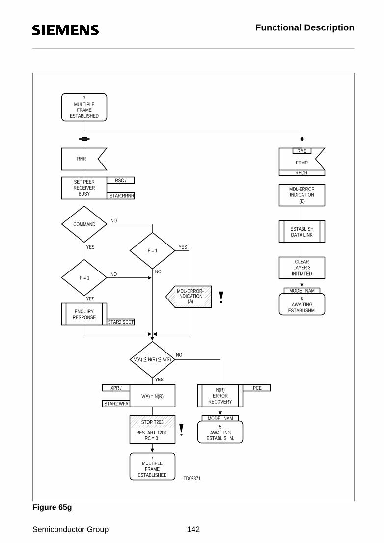
Functional Description
Figure 65g
ESTABLISHEDFRAME
MULTIPLE7
RNR
RECEIVERSET PEER
BUSY STAR:RRNR
RSC /
COMMANDNO
YESF = 1
YES
NOP = 1
YES
NO
ENQUIRYRESPONSE
STAR2:SDET
RHCR:
FRMR
RME
(K)
MDL-ERRORINDICATION
ESTABLISHDATA LINK
LAYER 3CLEAR
INITIATED
ESTABLISHM.AWAITING
5
MODE NAM
NO
YES
V(A) = N(R)STAR2:WFA
XPR /
RESTART T200RC = 0
ESTABLISHEDFRAME
MULTIPLE7
N(R)ERROR
RECOVERY
PCE
ESTABLISHM.AWAITING
5
MODE NAM
ITD02371
STOP T203
MDL-ERROR-INDICATION
(A)
V(A) N(R) V(S)_<_<
Semiconductor Group 142

Functional Description
Figure 65h
ESTABLISHEDFRAME
MULTIPLE7
COMMANDI
OWNRECEIVER
BUSY
YES
NO
N(S) = V(R)
V(R) = V(R) + 1
NO
YES
INFORMATIONDISCARD
EXCEPTIONCLEAR REJECT EXCEPTION
REJECT
RFIFO, RHCR
RME
DL-DATAINDICATION
P = 1
P = 1
ACKNOWLEDGEPENDING
F = P
YES
YES
YES
NO
NO
PENDINGACKNOWLEDGE
SETACKNOWLEDGE
PENDING PENDINGACKNOWLEDGE
CLEAR
TX RR
STAR2:SDET
STAR2:SDET
TX REJ
CLEARACKNOWLEDGE
PENDING
F = P
EXCEPTIONREJECT
SET
3
YES
NOTE 1
F = 1
PENDINGACKNOWLEDGE
CLEAR
TX RNR
STAR2:SDET
YES
P = 1
DISCARDINFORMATION
NO
NO
NO
NOTE 2
ITD02372
Figure 65i
Note 1 : Processing of acknowledge pending is described on figure 65i .Note 2 : This SDL - representation does not include the optional procedure in Appendix I.
Semiconductor Group 143

Functional Description
Figure 65i
3
ERRORN(R)
RECOVERY
PCE
ESTABLISHM.AWAITING
5
MODE NAM
NO
YES
YES
NO
STOP T200
V(A) = N(R)
STAR2:WFA
XPR /
N(R) = V(S)
ESTABLISHEDFRAME
MULTIPLE7
YES
ITD02373
PEERRECEIVER
BUSY
XPR /
STAR2:WFA
V(A) = N(R)
NO
N(R) = V(A)
NO
YES
V(A) = N(R)
RESTART T200
RESTART T203
V(A) N(R) V(S)<__< _<_<
Semiconductor Group 144
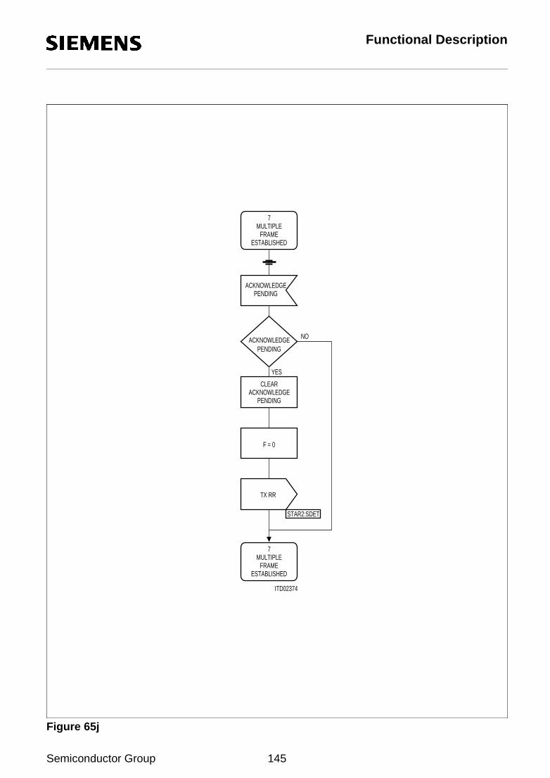
Functional Description
Figure 65j
ESTABLISHEDFRAME
MULTIPLE7
PENDINGACKNOWLEDGE
ACKNOWLEDGEPENDING
CLEARACKNOWLEDGE
PENDING
NO
YES
F = 0
TX RR
STAR2:SDET
ESTABLISHEDFRAME
MULTIPLE7
ITD02374
Semiconductor Group 145
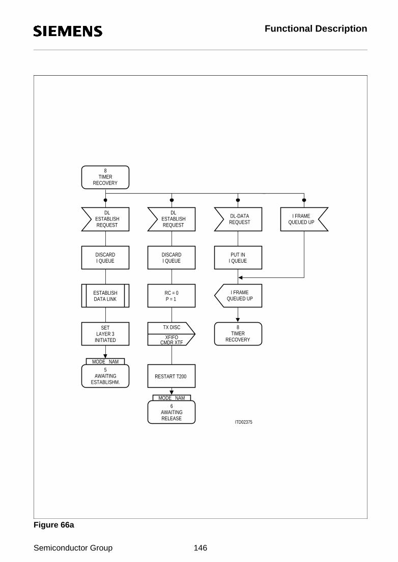
Functional Description
Figure 66a
MODE NAM
ITD02375
8TIMER
RECOVERY
DLESTABLISHREQUEST REQUEST
DL
DISCARDI QUEUE
DATA LINKESTABLISH
INITIATEDLAYER 3
SET
5AWAITING
ESTABLISHM.
I FRAMEQUEUED UPREQUEST
DL-DATA
I QUEUEDISCARD
I QUEUEPUT IN
RC = 0 P = 1
I FRAMEQUEUED UP
TX DISC
XFIFOCMDR XTF
RESTART T200
RELEASEAWAITING
6
MODE NAM
RECOVERYTIMER
8
ESTABLISH
Semiconductor Group 146

Functional Description
Figure 66b
DEACTIVATIONPERSISTENTMDL
REMOVEREQUEST
TIMERT200
EXPIRY
QUEUESI AND UI
DISCARD DISCARDI AND UIQUEUES
INDICATIONDL-RELEASE DL-RELEASE
INDICATION
STOP T200 STOP T200
TRANSMITENQUIRY
RC = RC + 1
RECOVERYTIMER
8
ITD02376
8TIMER
RECOVERY
TIMR TIMR
UNASSIGNEDTEI1
MODE NAM
ASSIGNEDTEI4
MODE NAM
INDICATION(I)MDL-ERROR
TIN
ESTABLISHDATA LINK
CLEARLAYER 3
INITIATED
MODE NAM
5AWAITING
ESTABLISHM.
RC = N200 YES
NO
NO
V(S) = V(A)YES
NO
YES
START T200
CLEARACKNOWLEDGE
PENDING
V(S) = V(S) + 1
TX ICOMMAND
P = 1V(S) = V(S) - 1
GET LASTTRANSMITTED
I FRAME
BUSYPEER
Semiconductor Group 147

Functional Description
Figure 66c
ITD02377
8TIMER
RECOVERY
I QUEUEDISCARD
STAR2:WFA = 0
V(S) = V(A)
TX UA
XFIFOCMDR XTF
I QUEUEDISCARD
NO
YES
RME
SABME
RHCR: RHCR:
DISC
RME
RHCR:
UA
RME
F = PMDL-ERRORINDICATION
(C, D)
CMDR XTFXFIFO
TX UA
CLEAREXCEPTIONCONDITIONS
(F)INDICATIONMDL-ERROR
DLESTABLISHINDICATION
DL-RELEASEINDICATION
CMDR:RHR;XRES
STOP T200
STOP T200
ASSIGNEDTEI4
MODE NAM
ESTABLISHEDFRAME
MULTIPLE7
WFASTAR2:STORE
V(R) = 0V(A) = 0V(S) = 0
F = PRECOVERY
TIMER8
STAR2:TREC
START T203
Semiconductor Group 148

Functional Description
Figure 66d
ITD02378
RHCR:
DM
RME
F = 1
RHCR
MDL-ERRORINDICATION
(E)
ESTABLISHDATA LINK
(B)INDICATIONMDL-ERROR
BUSYRECEIVERSET OWN
YES
NO NO
YESCLEARRECEIVER
BUSY
CMDR:RNR = 1BUSY
RECEIVERSET OWN
STAR:XRNR
ESTABLISHM.AWAITING
5
MODE NAM
F = 0
LAYER 3CLEAR
INITIATED
PENDING
CLEARACKNOWLEDGE ACKNOWLEDGE
CLEAR
PENDING
F = 0
STAR:XRNR
CLEAR OWNRECEIVER
BUSYCMDR:RNR = 0
BUSYRECEIVER
OWNNO
YES
CLEAR OWNRECEIVER
BUSY
Note: These signals are generated outside of this SDL representation,and may be generated by the connection management entity.
RECOVERYTIMER
8
RECOVERYTIMER
8
TX RNRRESPONSE
TX RRRESPONSE
Semiconductor Group 149

Functional Description
Figure 66e
RR
RECEIVERCLEAR PEER
BUSY STAR:RRNR
RSC /
COMMANDNO
YESF = 1
YES
NOP = 1
YES
NO
ENQUIRYRESPONSE
STAR2:SDET
REJ
RECOVERYTIMER
8
XPR /
STAR2:WFA
V(A)=N(R)
RETRANS-INVOKE
MISSION
XMR /
ESTABLISHEDFRAME
MULTIPLE7
RECOVERYN(R) ERROR
PCE
ESTABLISHM.AWAITING
5
MODE NAM
YES
NO
YES
NO
V(A) = N(R)
STAR2:WFA
XPR /
ITD02379
RECOVERYTIMER
8
STAR2:TREC
START T203
STOP T200
V(A) N(R) V(S)<__< _<_<
V(A) N(R) V(S)_<_< __<<
Semiconductor Group 150
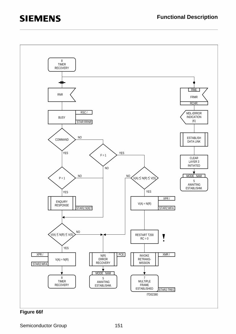
Functional Description
Figure 66f
RNR
BUSYSTAR:RRNR
RSC /
COMMANDNO
YESF = 1
YES
NOP = 1
YES
NO
ENQUIRYRESPONSE
STAR2:SDET
RCHR:
FRMR
RME
(K)
MDL-ERRORINDICATION
ESTABLISHDATA LINK
LAYER 3CLEAR
INITIATED
ESTABLISHM.AWAITING
5
MODE NAM
NO
YES
V(A) = N(R)STAR2:WFA
XPR /
ESTABLISHEDFRAME
MULTIPLE7
N(R)ERROR
RECOVERY
PCE
ESTABLISHM.AWAITING
5
MODE NAM
ITD02380
RECOVERYTIMER
8
YES
NO
RECOVERYTIMER
8
STAR2:TREC
XMR /
MISSIONRETRANS-
INVOKE
RESTART T200RC = 0
XPR /
STAR2:WFAV(A) = N(R)
V(A) N(R) V(S)_<_<
V(A) N(R) V(S)_<_<
Semiconductor Group 151

Functional Description
Figure 66g
RECOVERYTIMER
8
COMMANDI
OWNRECEIVER
BUSY
YES
NO
N(S) = V(R)
V(R) = V(R) + 1
NO
YES
INFORMATIONDISCARD
EXCEPTIONCLEAR REJECT
EXCEPTIONREJECT
RFIFO, RHCR
RME
DL-DATAINDICATION
P = 1
P = 1
ACKNOWLEDGEPENDING
F = P
YES
YES
YES
NO
NO
PENDINGACKNOWLEDGE
SETACKNOWLEDGE
PENDING PENDINGACKNOWLEDGE
CLEAR
TX RR
STAR2:SDET
STAR2:SDET
TX REJ
CLEARACKNOWLEDGE
PENDING
F = P
EXCEPTIONREJECT
SET
4
YES
NOTE 1
F = 1
PENDINGACKNOWLEDGE
CLEAR
TX RNR
STAR2:SDET
YES
P = 1
DISCARDINFORMATION
NO
NO
NO
NOTE 2
ITD02381
Figure 66hNote 1 : Processing of acknowledgeNote 2 : This SDL-representation does not include the optional procedure in Appendix I.
pending is descripted on figure 66i .
Semiconductor Group 152
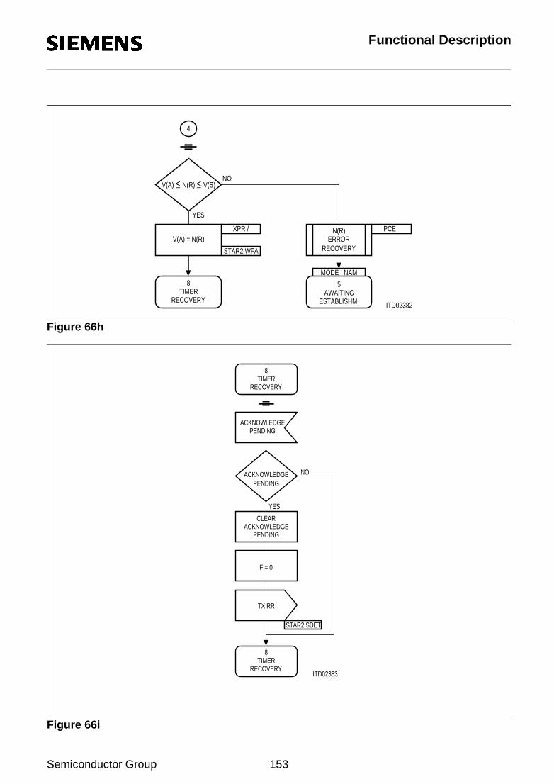
Functional Description
Figure 66h
Figure 66i
4
ERRORN(R)
RECOVERY
PCE
ESTABLISHM.AWAITING
5
MODE NAM
NO
YES
ITD02382
XPR /
STAR2:WFA
V(A) = N(R)
RECOVERYTIMER
8
V(A) N(R) V(S)_<_<
RECOVERYTIMER
8
PENDINGACKNOWLEDGE
ACKNOWLEDGEPENDING
CLEARACKNOWLEDGE
PENDING
NO
YES
F = 0
TX RR
STAR2:SDET
ITD02383
8TIMER
RECOVERY
Semiconductor Group 153

Functional Description
Figure 67a
(NOTE 1)STATES
RELEVANT
REQUESTUNIT DATA
DL UIFRAME
QUEUED UP
RMEUI COMMAND
RHCR
UI QUEUEPLACE IN
REMOVE UIFRAME FROM
QUEUE
DLUNIT DATAINDICATION
QUEUED UPFRAME
UIP = 0 NOTE 2
NOTE 2
NOTE 2
TX UICOMMAND
CMDR: XTFXFIFO
ITD02384
Note 1: The relevant states are as follows4 TEI-assigned5 Awaiting-establishement6 Awaiting-release7 Multiple-frame-established8 Timer-recovery
Note 2: The data link layer returns to the state it was in prior to the events shown.
Semiconductor Group 154

Functional Description
Figure 67b
(NOTE 1)STATES
RELEVANT
INFO NOTPERMITTED
(X)
CLEARLAYER 3
INITIATED
MDL-ERRORINDICATION
(L,M,N,O)
ITD02385
Note 1: The relevant states are as follows7 Multiple-frame-established8 Timer-recovery
ERROR (W)FIELD
CONTROL
(X)LENGHT
INCORRECT 1 FRAMETOO LONG
(Y)
ESTABLISHDATA LINK
ESTABLISHM.AWAITING
5
PCE /
Semiconductor Group 155

Functional Description
Figure 67c
(NOTE 1)STATES
RELEVANT
FIELDCONTROL
ITD02577
ERROR (W) (X)PERMITTEDINFO NOT I FRAME
TOO LONG (Y) (X)
INCORRECTLENGTH
(L, M, N, O)INDICATION
MDL-ERROR-
NOTE 2
Note 1:
Note 2:
The relevant states are as follows:4 TEI-assigned5 Awaiting-establishment6 Awaiting-releaseThe data link layer returns to the state it was in prior to the events shown
Semiconductor Group 156
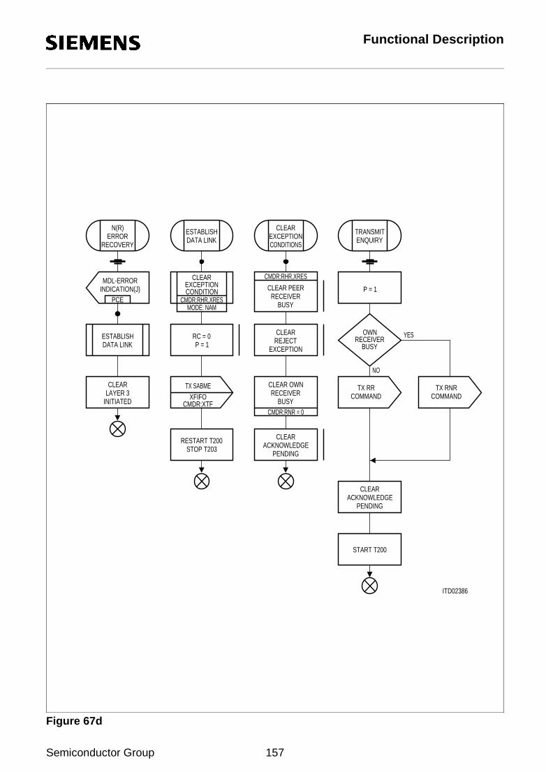
Functional Description
Figure 67d
ITD02386
N(R)ERROR
RECOVERY
INDICATION(J)MDL-ERROR
PCE
DATA LINKESTABLISH TRANSMIT
ENQUIRYCONDITIONSEXCEPTION
CLEAR
CLEAREXCEPTIONCONDITION
CMDR:RHR,XRESMODE: NAM
CLEAR PEERRECEIVER
BUSY
CMDR:RHR,XRES
P = 1
ESTABLISHDATA LINK P = 1
RC = 0
EXCEPTIONREJECTCLEAR
BUSYRECEIVER
OWN
CLEARLAYER 3
INITIATEDCMDR:RNR = 0
BUSYRECEIVER
CLEAR OWN
CMDR:XTFXFIFO
TX SABMECOMMAND
TX RR TX RNRCOMMAND
RESTART T200STOP T203
CLEARACKNOWLEDGE
PENDING
PENDINGACKNOWLEDGE
CLEAR
YES
NO
START T200
Semiconductor Group 157

Functional Description
Figure 67e
ITD02387
ENQUIRYRESPONSE
F = 1
BUSYRECEIVER
OWN
RESPONSETX RR TX RNR
RESPONSE
PENDINGACKNOWLEDGE
CLEAR
YES
NO
RETRANS-INVOKE
MISSION
V(S) = N(R)YES
NO
V(S) =V(S) - 1
XMR
QUEUED UPI FRAME
STAR2:SDET STAR2:SDET
BACK TRACKALONG
I QUEUE
NOTE
Note: The generation of the correct number of signals in order to cause the requiredretransmission of I frames does not alter their sequence integrity.
Semiconductor Group 158

Operational Description
3 Operational Description
The ISAC-S, designed for the connection of subscribers to an ISDN using a standard S/Tinterface, has the following applications, corresponding to the operating modes explained inchapter 2:
Terminal Equipment TE1, TA → TE mode
e.g. ISDN feature telephone,ISDN voice/data workstationTerminal Adapter for non-ISDN terminals (TE2)
Network termination NT2
e.g. PABX, including the following functions:
Line termination on S → LT-S modesuch as an IPBX S interface line card
Line termination on T → LT-T modeto connect an NT2 to an NT1 (digital trunk module)
Intelligent Network Termination → NT modee.g. NT1 with maintenance functions
The operating mode of the ISAC-S must be set via pin strapping (pins M1, M0), as describedin section 2.2, before a hardware reset.
Semiconductor Group 159

Operational Description
3.1 Microprocessor Interface Operation
The ISAC-S is programmed via an 8-bit parallel microcontroller interface. Easy and fastmicroprocessor access is provided by 8-bit address decoding on the chip. Depending on thechip package (P-DIP-40, P-LCC-44 or M-QFP-64) either one or three types of µP buses areprovided:
P-DIP-40 package:
The ISAC-S microcontroller interface is of the Siemens/Intel multiplexed address/data bustype with control signals CS, WR, RD, ALE.
P-LCC-44/P-MQFP-64 package:
The ISAC-S microcontroller interface can be selected to be either of the
(1) – Motorola type with control signals CS, R/W, DS
(2) – Siemens/Intel non-multiplexed bus type with control signals CS, WR, RD
(3) – or of the Siemens/Intel multiplexed address/data bus type with control signals CS, WR, RD, ALE.
The selection is performed via pin ALE as follows:
ALE tied to VDD ⇒ (1)
ALE tied to VSS ⇒ (2)
Edge on ALE ⇒ (3).
The occurrence of an edge on ALE, either positive or negative, at any time during the operationimmediately selects interface type (3). A return to one of the other interface types is possibleonly if a hardware reset is issued.
Notes: 1) If the multiplexed address/data bus type (3) is selected, the unused address pinsA0-A5 are internally not evaluated and may thus be left open. It is howeverrecommended to tie the unused input pins to a defined voltage level (e.g. VSS orVDD).
2) If the non-multiplexed bus types (1) or (2) are selected, the serial interfaces SLDand SSI can no longer be used since pin 5 (SDAR)/A2 and pin 10 (SIP/EAW)/A5now have the function of address pins. These µP bus types are therefore primarilyintended to be used in IOM-2 modes (ADF2:IMS=1).If however the PEB 2086 P-MQFP-64 package is used, the demultiplexed micro-processor interface is also available in IOM-1 mode.
Semiconductor Group 160
Operational Description
The microprocessor interface signals are summarized in table 11.
Table 11µP Interface of the ISAC®-S
Pin No.P-DIP-40
Pin No.P-LCC-44
Function
373839401234
414243441234
Multiplexed Bus Mode: Address/Databus. Transfers addresses from the µPsystem to the ISAC-S and data betweenthe µP system and the ISAC-S.Non-Multiplexed Bus Mode: Data bus.Transfers data between the µP system andthe ISAC-S.
34 37 Chip Select. A 0 ("low") on this line selectsthe ISAC-S for a read/write operation.
35
38
38
Read/Write. A 1 ("high"), identifies a validµP access as a read operation. A 0,identifies a valid µP access as a writeoperation (Motorola bus mode).Write. This signal indicates a writeoperation (Siemens/Intel bus mode).
36
39
39
Data Strobe. The rising edge marks theend of a valid read or write operation(Motorola bus mode).Read. This signal indicates a readoperation (Siemens/Intel bus mode).
20 23 Interrupt Request. The signal is activatedwhen the ISAC-S requests an interrupt. It isan open drain output.
33 36 Address Latch Enable. A high on this lineindicates an address on the externaladdress bus (Multiplexed bus type only).ALE also selects the µP interface type(multiplexed or non-multiplexed).
40 Address Bit 0 (Non-multiplexed bus type).
6 Address Bit 1 (Non-multiplexed bus type).
5 Address Bit 2 (Non-multiplexed bus type).
18 Address Bit 3 (Non-multiplexed bus type).
17 Address Bit 4 (Non-multiplexed bus type).
10 Address Bit 5 (Non-multiplexed bus type).
OD
A4
I
I
Input (I)Output (O)Open Drain(OD)
I/OI/OI/OI/OI/OI/OI/OI/O
I
I
I
I
I
I
I
I
I
I
Symbol
AD0/D0AD1/D1AD2/D2AD3/D3AD4/D4AD5/D5AD6/D6AD7/D7
CS
R/W
WR
DS
RD
INT
ALE
A0
A1
A2
A3
A5
Pin No.P-MQFP-64
3738394041424344
27
28
28
29
29
8
26
30
51
50
64
63
55
Semiconductor Group 161
Operational Description
3.2 Interrupt Structure and Logic
Since the ISAC-S provides only one interrupt request output (INT), the cause of an interrupt isdetermined by the microprocessor by reading the Interrupt Status Register ISTA. In thisregister, seven interrupt sources can be directly read. The LSB of ISTA points to eight non-critical interrupt sources which are indicated in the Extended Interrupt Register EXIR(figure 68).
Figure 68ISAC®-S Interrupt Structure
ITD02578
RMERPFRSCXPRTIN
CISQSINEXI EXI
SINCISQTINXPRRSCRPFRME
MASK ISTAXMRXDUPCERFOSOVMOSSAWWOVEXIR
MOSRMOCR
MDR1MER1MDA1MAB1MDR0MER0MDA0MAB0
MXE0
MRE0
MXE1
MRE1
INT
CIR0
SQCBAS
CIC0CIC1
SQIE
CI1E
SQXR
CIR1
SQRR
CODR0
onlyRIOM -2
Semiconductor Group 162
Operational Description
A read of the ISTA register clears all bits except EXI and CISQ. CISQ is cleared by readingCIR0. A read of EXIR clears the EXI bit in ISTA as well as the EXIR register.
When all bits in ISTA are cleared, the interrupt line (INT) is deactivated.
Each interrupt source in ISTA register can be selectively masked by setting to "1" thecorresponding bit in MASK. Masked interrupt status bits are not indicated when ISTA is read.Instead, they remain internally stored and pending, until the mask bit is reset to zero. Readingthe ISTA while a mask bit is active has no effect on the pending interrupt.
In the event of an extended interrupt and of a C/I or S/Q channel change, EXI and CISQ areset even when the corresponding mask bits in MASK are active, but no interrupt (INT) isgenerated.
Except for CISQ and MOS all interrupt sources are directly determined by a read of ISTA and(possibly) EXIR.
CISQ Interrupt logic
– A CISQ interrupt may originate
– from a change in the received S/Q code (SQC)
– from a change in the received C/I channel 0 code (CIC0)
or (in the case of IOM-2 terminal mode only)
– from a change in the received C/I channel 1 code (CIC1).
The three corresponding status bits SQC, CIC0 and CIC1 are read in the CIR0 register. SQCand CIC1 can be individually disabled by clearing the enable bit SQIE (SQXR register) or,respectively, CI1E (SQXR register). In this case the occurrence of a code change in SQRR/CIR1 will not be displayed by SQC/CIC1 until the corresponding enable bit has been set to one.
Bits SQC, CIC0 and CIC1 are cleared by a read of CIR0.
An interrupt status is indicated every time a valid new code is loaded in SQRR, CIR0 or CIR1.But in case of a code change, the new code is not loaded until the previous contents have beenread. When this is done and a second code change has already occurred, a new interrupt isimmediately generated and the new code replaces the previous one in the register. The coderegisters are buffered with a FIFO size of two. Thus, if several consecutive codes are detected,only the first and the last code is obtained at the first and second register read, respectively.
Semiconductor Group 163

Operational Description
MOS interrupt logic
The MOS interrupt logic shown in figure 68 is valid only in the case of IOM-2 interface mode.Further, only one MONITOR channel is handled in the case of IOM-2 non-terminal timing mo-des. In this case, MOR1 and MOX1 are unused.
The MONITOR Data Receive (MDR) and the MONITOR End of Reception (MER) interruptstatus bits have two enable bits, MONITOR Receive interrupt Enable (MRE) and MR bitControl (MRC). The MONITOR channel Data Acknowledged (MDA) and MONITOR channelData Abort (MAB) interrupt status bits have a common enable bit MONITOR Interrupt Enable(MXE).
MRE prevents the occurrence of the MDR status, including when the first byte of a packet isreceived. When MRE is active (1) but MRC is inactive, the MDR interrupt status is generatedonly for the first byte of a receive packet. When both MRE and MRC are active, MDR is gene-rated and all received monitor bytes – marked by a 1-to-0 transition in MX bit – are stored. (Ad-ditionally, an active MRC enables the control of the MR handshake bit according to the MONI-TOR channel protocol.)
In IOM-1 mode the reception of a monitor byte is immediately indicated by the MOS interruptstatus, and registers MOCR and MOSR are not used.
Control of edge-triggered interrupt controllers
The INT output is level active. It stays active until all interrupt sources have been serviced. Ifa new status bit is set while an interrupt is serviced, the INT line stays active. This may causeproblems if the ISAC-S is connected to edge-triggered interrupt controllers (figure 69).To avoid these problems, it is recommended to mask all interrupts at the end of the interruptservice program and to enable the interrupts again. This is done by writing FFH to the MASKregister and to write back the old value of the MASK register (figure 70).
Semiconductor Group 164

Operational Description
Figure 69INT Handling
Figure 70Service Program for Edge-Triggered Interrupt Controllers
INT
➀ ➂
➁ ➃
➄
➀ A status bit is set. This causes an interrupt.
➁ The microprocessor starts its service routine and reads the status registers.
➂ A new status bit is set before the first status bit has been read.
➃ The first status bit is read.
➄ The INT output stays active but the interrupt controller will not serve the interrupt(edge triggered).
INT
➀ ➂
➁ ➃ ➄ ➅ ➆ ➇ ➈
➀ to ➃ see above
➄ ’FF’ is written to the MASK register. This masks all interrupts and returns the INToutput to its inactive state.
➅ The old value is written to the MASK register. This will activate the INT output ifan interrupt source is still active.
➆ The microprocessor starts a new interrupt service program.
➇ The last status bit is read.
➈ The INT output is inactive.
Semiconductor Group 165

Operational Description
Figure 71Timing of INT Pin
The INT line is switched with the rising edge of DCL. If no pending interrupts are internallystored, a reading of ISTA respectively EXIR or CIR0 switches the INT line to high as indicatedin figure 71.
3.3 Control of Layer 1
3.3.1 Activation/Deactivation of IOM® Interface
In LT-T and LT-S applications the IOM interface should be kept active, i.e. the clock DCL andthe frame sync FSC1/2 (inputs) should always be supplied by the system.
In TE and NT applications the IOM interface can be switched off in the inactive state,reducing power consumption to a minimum. In this deactivated state the clock line is low andthe data lines are high.
In TE mode the IOM interface can be kept active while the S interface is deactivated by settingthe CFS bit to "0" (ADF1 register in IOM-1, SQXR register in IOM-2 mode). This is the caseafter a hardware reset. If the IOM interface should be switched off while the S interface isdeactivated, the CFS bit should be set to "1". In this case the internal oscillator is disabledwhen no signal (info 0) is present on the S bus. If the TE wants to activate the line, it has firstto activate the IOM interface either by using the "Software Power Up" function (SPCR:SPU bit)or by setting the CFS bit to "0" again.
For the TE case the deactivation procedure is shown in figure 72. After detecting the code DIU(Deactivate Indication Upstream, i.e. from TE to NT/LT-S) the layer 1 of the ISAC-S respondsby transmitting DID (Deactivate Indication Downstream) during subsequent frames and stopsthe timing signals synchronously with the end of the last C/I (C/I0) channel bit of the fourthframe.
ITD02388
~~~ ~
~~
DCL
INT
RD
Semiconductor Group 166

Operational Description
Figure 72Deactivation of the IOM® Interface
ITD02343
DIU DIU
DR
FSC1/2
IDP1
IDP2
Deactivated(a)
DIU DIU DIU DIU
DR DID DID DID DID
RIOM -1 RIOM
ITD02579
DIU DIU DIU DIU DIU DIU DIU DIU DIU
DIDDIDDIDDIDDRDRDRDRDR
FSC
IDP1
IDP0
Deactivated
D
B2 MONO DB1
CIO
CIO
(b)
DCL
RIOM -2 -2IOM R
Semiconductor Group 167
Operational Description
The clock pulses will be enabled again when the IDP1 line is pulled low (bit SPU, SPCRregister) i.e. the C/I command TIM = "0000" is received by layer 1, or when a non-zero levelon the S-line interface is detected. The clocks are turned on after approximately 0.2 to 4 msdepending on the capacitances on XTAL 1/2.
DCL is activated such that its first rising edge occurs with the beginning of the bit following theC/I (C/I0) channel.
After the clocks have been enabled this is indicated by the PU code in the C/I channel and,consequently, by a CISQ interrupt. The IDP1 line may be released by resetting the SoftwarePower Up bit SPCR:SPU=0, and the C/I code written in CIX0 is output on IDP1.
(a) IOM®–1
Figure 73Activation of the IOM ® Interface (CFS=1, Register ADF1 (IOM®-1)/SQXR (IOM®-2))
ITD02389
IDP1
~ ~
IDP0 ~~
FSC1/2
~ ~
DCL
PUPUPU
(AR)
SPU = 0
CISQ Int.
1=SPU
0.2 to 4 ms
4 x DCL
Semiconductor Group 168

Operational Description
(b) IOM®–2
ITD02390
~ ~~~
~ ~~~
~ ~ ~~
~ ~~ ~
~ ~
~ ~~~
~ ~~~~~
~~FSC
IDP1
IDP0
FSC
IDP1
IDP0
DCL
SPU = 1 0=SPUCIS0 = TIMCISQ
Int.
TIM TIM TIM
PU PU PU PU PU
-CH1 B1
B1MXMR
0.2 to 4 ms
132 x DCL
Note : IDP0 is input and IDP1 is low during IOM -CH1 if : IDC = 1
0=IDC:IDP0 is low and IDP1 is input during IOM -CH1 if
RIOM
RIOM -CH1
RIOM -CH2
IOM -CH2R
RSQXR
SQXR R
Semiconductor Group 169

Operational Description
The ISAC-S supplies IOM timing signals as long as there is no DIU command in the C/I (C/I0)channel. If timing signals are no longer required and activation is not yet requested, this isindicated by programming DIU in the CIX0 register.
As an alternative to activation via IDP1 (DU), the IOM interface can be activated by setting theCFS bit to "0". The activation of FSC1 and DCL in this case is similar to figure 73. Note thatthe IOM interface can be deactivated through DIU (power-down state, figure 72) only if CFSis set to logical "1".
In NT mode the IOM interface is activated by the upstream unit turning on the clocking signals.Simultaneously the upstream unit must send the desired command in the C/I channel. In thecase where activation is requested from a terminal, the layer 1 of ISAC-S in the NT firstrequests timing on the IOM interface by pulling IDP0 to a static low level which causes a CISQinterrupt. Power-up state is entered immediately after timing has been applied. The clocksignals may be switched off after the code Deactivation Indication Downstream has been senttwice by the upstream unit.
3.3.2 Activation/Deactivation of S/T Interface
Assuming the ISAC-S has been initialized with the required features of the application, it is nowready to transmit and receive messages in the D channel (LAPD support).
But as a prerequisite, the layer 1 has to be activated.
The layer-1 functions are controlled by commands issued via the CIXR/CIX0 register. Thesecommands, sent over the IOM C/I channel 0 to layer 1, trigger certain procedures, such asactivation/deactivation, switching of test loops and transmission of special pulse patterns.These are governed by layer-1 state diagrams in accordance with CCITT I.430. Responsesfrom layer 1 are obtained by reading the CIRR/CIR0 register after a CISQ interrupt (ISTA).
The state diagrams are shown in figures to . The activation/deactivation implemented by theISAC-S in its different operating modes agrees with the requirements set forth in CCITTrecommendations. State identifiers F1-F8 (TE/LT-T) and G1-4 (NT/LT-S) are in accordancewith CCITT I.430. In the NT mode the four states have been expanded to implement a fullhandshake between the ends of the subscriber loop.
In the state diagrams a notation is employed which explicitly specifies the inputs and outputson the S interface and in the C/I channel: see figure 74.
Semiconductor Group 170

Operational Description
Figure 74
3.3.2.1 Layer-1 Command/Indication Codes and State Diagrams in TE/LT-T Modes
Table 12Commands TE/LT-T
Important Note: In IOM-2 mode (ADF2:IMS=1), when in the activated state (AI8/AI10indication) the 2B+D channels are only transferred from the IOM-2 to the S/T interface if an "Activate Request" command is written to the CIX0 register.
ITD02331
i i
Cmd.Ind.
State
S-INFO
C /
UnconditionalTransitionX Y
RISAC -S INRISAC -S OUT
Ι
RemarksCommand (upstream) Abbr. Code
Activation of all output clocks is requestedTiming TIM 0000
(x)Reset RS 0001
Transmission of pseudo-ternary pulses at96 kHz frequency (x)
Send continuous zeros SCZ 0100
Transmission of pseudo-ternary pulses at2 kHz frequency (x)
Send single zeros SSZ 0010
Activation command, set D-channelpriority to 8 (see note)
Activate request, set priority 8 AR8 1000
Activation command, set D-channelpriority to 10 (see note)
Activate request, set priority 10 AR10 1001
Activation of test loop 3 (x)Activate request loop ARL 1010
IOM interface clocks can be disabledDeactivate indication upstream DIU 1111
(x) unconditional commands
Semiconductor Group 171

Operational Description
Table 13Indications TE/LT-T
*) Note: The X0 pin of the PEB 2085 ISAC-S which was intended for the CON-input(Connected to the S-Bus) has been eliminated on the PEB 2086. As a result, the C/I response DIS (Disconnect) will not be generated on the PEB 2086.
RemarksIndication (downstream) Abbr. Code
IOM clocking is providedPower up PU 0111
Deactivation request by S interfaceDeactivate request DR 0000
Wander is larger than 24 µs peak-to-peak (LT-T mode only)
Slip detected SD 0010
Pin CON connected to GND*Disconnected DIS 0011
Either: (pin RST = 1 and bit CFS = 0) or RSError indication EI 0110
Signal received, receiver not synchronousLevel detected RSY 0100
Info 2 receivedActivate request downstream ARD 1000
Test loop 3 activated or continuous zeros transmitted
Test indication TI 1010
Level detected during test loopAwake test indication ATI 1011
Info 4 received, D-channel priority is 8 or 9Activate indication withpriority class 8
AI8 1100
Info 4 received, D-channel priority is 10 or11
Activate indication withpriority class 10
AI10 1101
Clocks will be disabled in TE, quiescentstate
Deactivate indicationdownstream
DID 1111
Semiconductor Group 172
Operational Description
F3 Power Down
This is the deactivated state of the physical protocol. The receive line awake unit is activeexcept during an RST pulse. Clocks are disabled if ADF1/SQXR:CFS=1 (TE mode). Thepower consumption in this state is approximately 80 mW when the clock is running, and 8 mWotherwise.
F3 Power Up
This state is identical to "F3 power down", except for the C/I output message. The state isinvoked by a C/I command TIM = "0000" (or IDP1 static low). After the subsequent activationof the clocks the PU message is outputted. This occurs 0.5 ms to 4 ms after application of TIM,depending on crystal capacitances. If, however, the ISAC-S is disconnected from the Sinterface (CON = 0), the C/I message DIS is outputted.
F3 Pending Deactivation
The ISAC-S reaches this state after receiving INFO0 (from states F5 to F8) for 16 ms (64frames). This time constant is a "flywheel" to prevent accidental deactivation. From this statean activation is only possible from the line (transition "F3 pend. deact." to "F5unsynchronized"). A power down state may be reached only after receiving DIU.
F4 Pending Activation
Activation has been requested from the terminal, INFO1 is transmitted, INFO0 is still received,"Power Up" is transmitted in the C/I channel. This state is stable: timer T3 (I.430) is to beimplemented in software.
F5 Unsynchronized
At the reception of any signal from the NT, the ISAC-S ceases to transmit INFO1 and awaitsidentification of INFO2 or INFO4. This state is reached at most 50 µs after a signal differentfrom INFO0 is present at the receiver of the ISAC-S.
F6 Synchronized
When the ISAC-S receives an activation signal (INFO2), it responds with INFO3 and waits fornormal frames (INFO4). This state is reached at most 6 ms after an INFO2 arrives at the ISAC-S (when the oscillator was disabled in "F3 power down").
F7 Activated
This is the normal active state with the layer-1 protocol activated in both directions. Note thatin IOM-2 mode the 2B+D channels can only be transmitted to the SIT interface if an "ActivationRequest" command is written to the CIX0 register. From state "F6 synchronized", state F7 isreached at most 0.5 ms after reception of INFO4. From state "F3 power down" with theoscillator disabled, state F7 is reached at most 6 ms after the ISAC-S is directly activated byINFO4.
Semiconductor Group 173

Operational Description
F8 Lost Framing
This is the condition where the ISAC-S has lost frame synchronization and is awaiting re-synchronization by INFO2 or INFO4 or deactivation by INFO0.
Unconditional States
Loop 3 Closed
On Activate Request Loop command, INFO3 is sent by the line transmitter internally to the linereceiver (INFO0 is transmitted to the line). The receiver is not yet synchronized.
Loop 3 Activated
The receiver is synchronized on INFO3 which is looped back internally from the transmitter.Data may be sent. The indication "TI" or "ATI" is output depending on whether or not a signaldifferent from INFO0 is detected on the S interface.
Test Mode Continuous Pulses
Continuous alternating pulses are sent.
Test Mode Single Pulses
Single alternating pulses are sent (2-kHz repetition rate).
Reset State
A software reset (RS) forces the ISAC-S to an idle state where the analog components aredisabled (transmission of INFO0) and the S line awake detector is inactive. Thus activationfrom the NT is not possible. Clocks are still supplied (TE mode) and the outputs are in a lowimpedance state.
The reset state should be left only with a "Deactivation Indication Upstream" (DIU) commandbefore any other command is given.
Semiconductor Group 174

Operational Description
Figure 75aState Diagram of TE/LT-T Mode
ITD02332
F3 Power Down
DID DIU
i0i0
i0 i0
TIMDIS
F3 Power Up
i1 i0
ARUPU
F4 Pend. Act.
F5 Unsynchroniz.
RSYD X
i0i0
F6 Synchronized
ARD X
i2i3
i0 i0
ARUDR
F3 Pend. Deact.F8 Lost Framing
F7 Activated
Uncond. States
X
ix iy
Cmd.Ind.
State
PUDIU
TIM
DIU
CON
i0
ARU
i0
RST TIM
TIM
TIM
X
DIUi0
i2
CON
ARU
i0
i0
i0 DIU
RSYD X
i0i0
SDAID ARU
i3 i4
i4
i0
i2
i4
i0
i0
i4
i2
i0
INOUT
S
X: Unconditional Commandcan be : ARL, RES, TM, SSP
i0
RIOM
Semiconductor Group 175

Operational Description
Figure 75bState Diagram of TE/LT-T Mode: Unconditional Transitions
ITD02333
PU ARL
*i3
ix iy
Cmd.Ind.
State
ARL
INOUT
S
X : Forcing Commandscan be : ARL, RES, TM, SSP
i0
ARLATI
i3
i3
X
X X
Reset State
EI RS
i0
RS
SCZ
ic
SCZTI
Test Mode
X
SSZ
X
TI
Loop Continuous Puls.3 Closed
Activated3Loop
1)
i0i3 1) *
*
*
Single PulsesTest Mode
Any SSZ
is
Ind.
1) : Only Internally
Single Pulses,:is
Test Pulses,ic :4
96 kHz
kHz
RIOM
Semiconductor Group 176

Operational Description
3.3.2.2 Layer-1 Command/Indication Codes and State Diagrams in LT-S Mode
Table 14Commands and Indications in LT-S Mode
(x) unconditional commands
RemarksCommand (downstream) Abbr. Code
(x)Deactivate request DR 0000
Transmission of pseudo-ternary pulses at96 kHz frequency (x)
Send continuous zeros SCZ 0001
Transmission of pseudo-ternary pulses at2 kHz frequency (x)
Send single zeros SSZ 0010
Activate request downstream ARD 1000
Activation request for loop 2Activate request loop ARL 1010
Deactivation acknowledgement, quiescent state
Deactivate indicationdownstream
DID 1111
RemarksIndication (upstream) Abbr. Code
No receive signalLost signal level LSL 0001
Receiver is not synchronousLost framing upstream RSYU 0100
Info 1 receivedActivate request upstream ARU 1000
Synchronous receiverActivate indication upstream AIU 1100
Timer (32 ms) expired or info 0 received(during 16 ms) after deactivation request
Deactivate indication upstream DIU 1111
Semiconductor Group 177

Operational Description
G1 Deactivated
The ISAC-S is not transmitting. No signal detected on the S interface, and no activationcommand is received in the C/I channel.
G2 Synchronized
As a result of an INFO1 detected on the S line or an ARD command, the ISAC-S beginstransmitting INFO2 and waits for reception of INFO3. INFO2 is sent after the awake detectorhas detected pulses during 4 ms. The timer to supervise reception of INFO3 is to beimplemented in the software.
G3 Activated
Normal state where INFO4 is transmitted to the S interface. This state is reached less than2 ms after an INFO3 first arrives at the ISAC-S receiver. The ISAC-S remains in this state aslong as neither a deactivation or a test mode is requested, nor a reset pulse is issued.
When receiver synchronism is lost, INFO2 is sent automatically. After reception of INFO3, thetransmitter keeps on sending INFO4.
G4 Pending Deactivation
This state is triggered by a deactivation request DR. It is an unstable state: indication DIU(state "G4 unacknowledged") is issued by the ISAC-S when:
– either INFO0 is received during 16 ms,
– or an internal timer of 32 ms expires.
G4 Unacknowledged
Final state after a deactivation request. The ISAC-S remains in this state until a response toDIU (in other words DID) is issued, without which a new activation is impossible.
Test Mode Continuous Pulses
Continuous alternating pulses are sent.
Test Mode Single Pulses
Single alternating pulses are sent (2-kHz repetition rate).
Semiconductor Group 178

Operational Description
Figure 76State Diagram of LT-S Mode
ITD02334
ix iy
Cmd.Ind.
State
INOUT
S
TIU : Transparent Indication Upstreamcan be : AIU, RSYU, LSL
SCZ
ic
TMDIU
Test ModeContinuous Puls.
*
Single Pulses,:is
Continuous Pulses,ic :4
96 kHz
kHz
DID
*
Continuous Puls.Test ModeDIU SSP
is i0
DRTIU
G4 Pend. Deact.
*
TIU SSZ
DR
DR
*
G4 Unackn.
DIU DR
i0
G1 Deactivated
DIU DID
i0
RST
G2 Synchronized
ARU DID
i2
G3 Activated
TIU
i2/i4
i0
DID
(i0 during 16(32 ms timeout)
ms) or
ARD
i1i0
ARD
i3
+ i1
AnyInfo
ARDDID
RIOM
Semiconductor Group 179
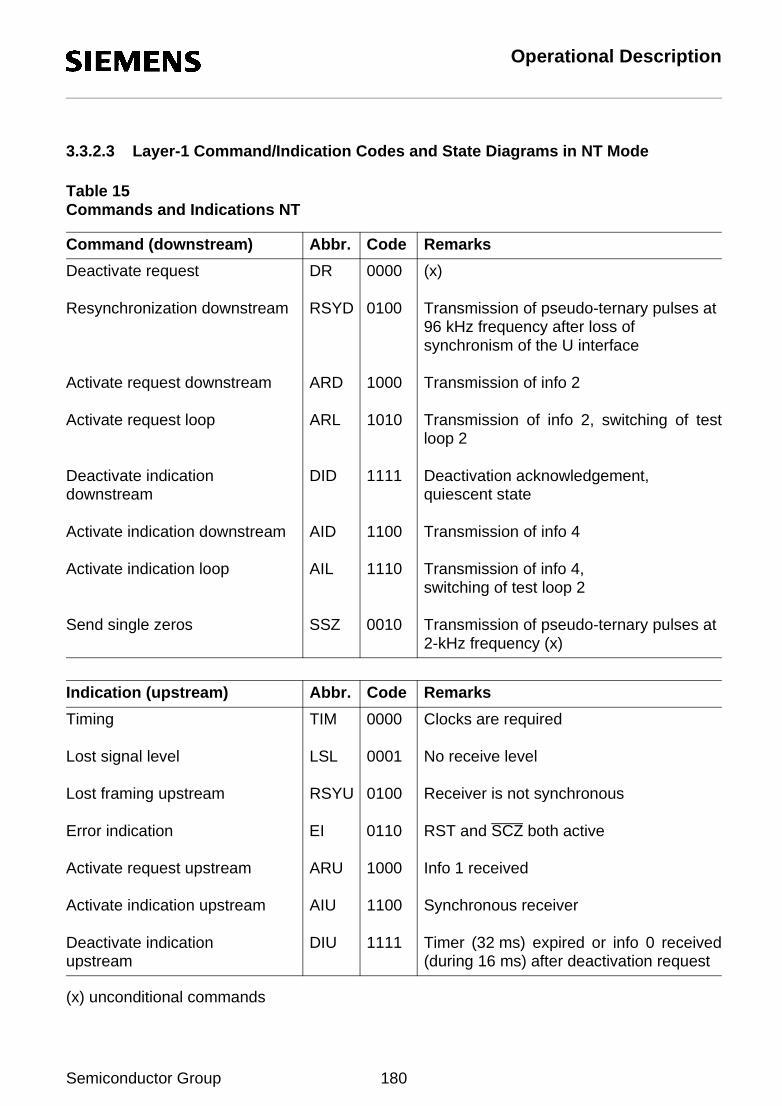
Operational Description
3.3.2.3 Layer-1 Command/Indication Codes and State Diagrams in NT Mode
Table 15Commands and Indications NT
(x) unconditional commands
RemarksCommand (downstream) Abbr. Code
(x)Deactivate request DR 0000
Transmission of pseudo-ternary pulses at 96 kHz frequency after loss of synchronism of the U interface
Resynchronization downstream RSYD 0100
Transmission of info 2Activate request downstream ARD 1000
Transmission of info 2, switching of testloop 2
Activate request loop ARL 1010
Deactivation acknowledgement,quiescent state
Deactivate indicationdownstream
DID 1111
Transmission of info 4Activate indication downstream AID 1100
RemarksIndication (upstream) Abbr. Code
Clocks are requiredTiming TIM 0000
No receive levelLost signal level LSL 0001
Receiver is not synchronousLost framing upstream RSYU 0100
RST and SCZ both activeError indication EI 0110
Info 1 receivedActivate request upstream ARU 1000
Transmission of info 4,switching of test loop 2
Activate indication loop AIL 1110
Transmission of pseudo-ternary pulses at 2-kHz frequency (x)
Send single zeros SSZ 0010
Synchronous receiverActivate indication upstream AIU 1100
Timer (32 ms) expired or info 0 received(during 16 ms) after deactivation request
Deactivate indicationupstream
DIU 1111
Semiconductor Group 180

Operational Description
G1 Deactivated
The ISAC-S is not transmitting. No signal is detected on the S/T interface, and no activationcommand is received in the C/I channel. EI is output as a response to RST, DIU is output inthe normal deactivated state, and TIM is output as a first step when an activation is requestedfrom the S/T interface.
G1 INFO1 Detected
An INFO1 is detected on the S/T interface, translated to an "Activation Request Upstream"indication in the C/I channel. The ISAC-S is waiting for an ARD command, which normallyindicates that the transmission line upstream (usually a two-wire interface) is synchronized.
G2 Pending Activation
As a result of the ARD command, an INFO2 is sent on the S/T interface. INFO3 is not yetreceived.
G2 Synchronized
INFO3 was received, INFO2 continues to be transmitted while the ISAC-S waits for a "switch-through" command AID from the device upstream.
G3 Activated
INFO4 is sent on the S/T interface as a result of the "switch through" command AID: the B andD channels are transparent. In case of loss of synchronism of the NT receiver, INFO2 is sent.
Lost Framing U
On receiving an RSYD command which usually indicates that synchronization has been loston the two-wire interface, the ISAC-S transmits continuous alternating pulses.
G4 Pending deactivation
This state is triggered by a deactivation request DR, and is an unstable state. Indication DIU(state "G4 unacknowledged") is issued by the ISAC-S when:
– either INFO0 is received during 16 ms
– or an internal timer of 32 ms expires.
G4 Unacknowledged
Final state after a deactivation request. The ISAC-S remains in this state until an"acknowledgement" to DIU (DID) is issued, without which a new activation is impossible.
Test Mode Continuous Pulses
Continuous alternating pulses are sent.
Test Mode Single Pulses
Single alternating pulses are sent (2-kHz repetition rate).
Semiconductor Group 181

Operational Description
Figure 77State Diagram of NT Mode
ix iy
Cmd.Ind.
State
INOUT
S
TIU : Transparent Indicationcan be : AIU, RSYU, LSL
SCZ
ic
DIU
Test ModeContinuous Puls.
*
Single Pulses,:is
Continuous Pulses,ic :4
96 kHz
kHz
DID
*
Single PulsesTest Mode
is i0
DRTIU
G4 Pend. Deact.
*
DR
*
G4 Unackn.
DIU DR
i0
G1 Deactivated
TIM, DID
i0
RST
G1 i1 Detected
ARU DID
G2 Pend. Act.
ARU
i0
DID
(i0 during 16(32 ms timeout)
ms) or
ARD
i1
ARD
SSZ* DIU *
InfoAny
TIU
Lost Framing U
ITD02335
ic
RSYD
DIUEI
i0 i1
i2 i3
AID
i2/i4
G3 Activated
TIU
AnyInfoInfo
Any
AIU
G2 Synchronized
i2
ARD
ARD
i3
AIU
AID
RSYDARD
RSYD
AID
RSYD
RIOM
Semiconductor Group 182

Operational Description
3.3.3 Example of Activation/Deactivation
An example of an activation/deactivation of the S interface, with the time relationshipsmentioned in the previous chapters, is shown in figure 78, in the case of an ISAC®-S in TE andLT-S modes.
Figure 78Example of Activation/Deactivation
INFO 0
AR
TE LT-S
INFO 2
AIUINFO 4
INFO 3
INFO 1
ARD
AID
ARU
RSYD
INFO 0
INFO 0
DIU
DR
DR
ITD02346
32 m
s
16 m
s4
ms
16 m
sm
ax. 6
ms
max
. 2 m
s
0.5
ms
Semiconductor Group 183

Operational Description
3.4 Control of Layer-2 Data Transfer
The control of the data transfer phase is mainly done by commands from the µP to ISAC-S viathe Command Register (CMDR).
Table 16 gives a summary of possible interrupts from the HDLC controller and the appropriatereaction to these interrupts.
Table 17 lists the most important commands which are issued by a microprocessor by settingone or several bits in CMDR.
The powerful FIFO logic, which consists of a 2 × 32 byte receive and 2 × 32 byte transmit FIFO,as well as an intelligent FIFO controller, builds a flexible interface to the upper protocol layersimplemented in the microcontroller.
The extent of LAPD protocol support is dependent on the selected message transfer mode,see section 2.4.2.
Table 16Interrupts from ISAC®-S HDLC Controller
MeaningMnemonic Register(addr. hex)
Reaction
Receive Pool Full. Request to read received bytes of an uncompleted HDLC frame from RFIFO
RPF ISTA (20) Read 32 bytes from RFIFO and acknowledge with RMC.
Receive Message End. Request to read received bytes of a complete HDLC frame (or the last part of a frame) from RFIFO.
RME ISTA (20) Read RFIFO (number of bytes given by RBCL4-0) and status information and acknowledge with RMC.
Receive Frame Overflow. A complete frame has been lost because storage space in RFIFO was not available.
RFO EXIR (24) Error report for statistical purposes. Possible cause: deficiency in software.
Protocol Error. S or I-frame with incorrect N(R) or S frame with I-field received (in auto mode only) or an I-frame which is not a command orS-frame with an undefined control field.
PCE EXIR (24) Link re-establishment. Indication to layer 3.
Layer-2 Receive
Semiconductor Group 184

Operational Description
MeaningMnemonic Register(addr. hex)
Reaction
Transmit Pool Ready. Further octets of an HDLC frame can be written to XFIFO.If XIFC was issued (auto mode), indicates that the message was successfully acknowledged with S frame.
XPR ISTA (20) Write data bytes in the XFIFO if the frame currently being transmitted is not finished or a new frame is to be transmitted, and issue an XIF, XIFC, XTF or XTFC command. In auto mode applications read the information in chapter 2.5.5.2.
Transmit Message Repeat. Frame must be repeated because of a transmission error (all HDLC message transfer modes) or a received negative acknowledgement (auto mode only) from peer station.
XMR EXIR (24) Transmission of the frame must be repeated. No indication to layer 3.
Transmit Data Underrun. Frame has been aborted because the XFIFO holds no further data and XME (XIFC or XTFC) was not issued.
XDU EXIR (24) Transmission of the frame must be repeated. Possible cause: excessive software reaction times.
Receive Status Change.A status change from peer station has been received (RR or RNR frame), auto mode only.
RSC ISTA (20) Stop sending new I-frames.
Layer-2 Transmit
Timer Interrupt. External timer expired or, in auto mode, internal timer (T200) and repeat counter (N200) bothexpired.
TIN ISTA (20) Link re-establishment. Indication to layer 3. (auto mode)
Semiconductor Group 185

Operational Description
Table 17List of Commands (CMDR (21) Register)
Bit 7…0CommandMnemonic
HEX Meaning
1000 0000RMC 80 Receive Message Complete. Acknowledges a block (RPF) or a frame (RME) stored in the RFIFO.
0100 0000RRES 40 Reset HDLC Receiver. The RFIFO is cleared. The transmit and receive counters (V(S), V(R)) are reset (auto mode).
0010 0000RNR 20 Receiver Not Ready (auto mode). An I- or S-frame will be acknowledged with RNR frame.
0001 0000STI 10 Start Timer.
0000 1010XTFC(XTF+XME)
0A Transmit Transparent Frame and Close. Enables the "transparent" transmission of the block entered last in the XFIFO. The frame is closed with a CRC and a flag.
0000 0110XIFC(XIF+XME)
06 Transmit I-frame and Close. Enables the "auto mode" transmission of the block entered last in the XFIFO. The frame is closed with a CRC and a flag.
0000 1000XTF 08 Transmit Transparent Frame. Enables the "transparent" transmission of the block entered last in the XFIFO without closing the frame.
0000 0100XIF 04 Transmit I-frame. Enables the "auto mode" transmission of the block entered last in the XFIFO without closing the frame.
0000 0001XRES 01 Reset HDLC Transmitter. The XFIFO is cleared.A frame currently in transmission will be aborted and closed by an abort sequence (7 "1").
Semiconductor Group 186
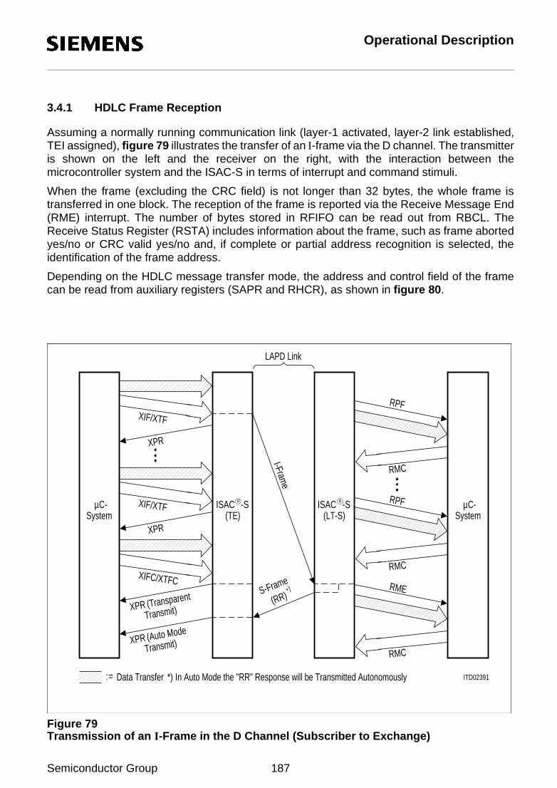
Operational Description
3.4.1 HDLC Frame Reception
Assuming a normally running communication link (layer-1 activated, layer-2 link established,TEI assigned), figure 79 illustrates the transfer of an I-frame via the D channel. The transmitteris shown on the left and the receiver on the right, with the interaction between themicrocontroller system and the ISAC-S in terms of interrupt and command stimuli.
When the frame (excluding the CRC field) is not longer than 32 bytes, the whole frame istransferred in one block. The reception of the frame is reported via the Receive Message End(RME) interrupt. The number of bytes stored in RFIFO can be read out from RBCL. TheReceive Status Register (RSTA) includes information about the frame, such as frame abortedyes/no or CRC valid yes/no and, if complete or partial address recognition is selected, theidentification of the frame address.
Depending on the HDLC message transfer mode, the address and control field of the framecan be read from auxiliary registers (SAPR and RHCR), as shown in figure 80.
Figure 79Transmission of an I-Frame in the D Channel (Subscriber to Exchange)
ITD02391
SystemC-µ
(TE) System(LT-S)
LAPD Link
XIF/XTF
XPR
XPR
XIF/XTF
XIFC/XTFC
XPR (Transparent
Transmit)
Transmit)(Auto Mode
XPR
I-Frame
S-Frame
(RR))
:= Data Transfer
*
*) In Auto Mode the "RR" Response will be Transmitted Autonomously
RPF
RMC
RPF
RMC
RME
RMC
-
C-µRISAC -S ISAC R -S
Semiconductor Group 187

Operational Description
Figure 80Receive Data Flow
Note 1 Only if a 2-byte address field is defined (MDS0 = 1 in MODE register).
Note 2 Comparison with Group TEI (FFH) is only made if a 2-byte address field is defined(MDS0 = 1 in MODE register).
Note 3 In the case of an extended, modulo 128 control field format (MCS = 1 in SAP2register) the control field is stored in RHCR in compressed form (I frames).
Note 4 In the case of an extended control field, only the first byte is stored in RHCR, thesecond in RFIFO.
A frame longer than 32 bytes is transferred to the microcontroller in blocks of 32 bytes plus oneremainder block of length 1 to 32 bytes. The reception of a 32-byte block is reported by aReceive Pool Full (RPF) interrupt and the data in RFIFO remains valid until this interrupt isacknowledged (RMC). This process is repeated until the reception of the remainder block iscompleted, as reported by RME (figure 79). When the total frame length exceeds 4095 bytes,bit OV (RBCH) is set but the counter is not blocked. If the second RFIFO pool has been filledor an end-of-frame is received while a previous RPF or RME interrupt is not yet acknowledged
ITD02342
Description of Symbols:
Checked automatically by
Compared with Register or Fixed Value
Stored Info Register or RFIFO
Flag HighAddress Address
Low Control Information CRC Flag
RSTARHCRFFTEI1, TEI2SAP1, SAP2
FE, FC
(Note 1) 2)(Note (Note 3)
RFIFO
RFIFOFE, FCSAP1, SAP2 TEI1, TEI2
FF RHCR RSTA
4)(Note (Note 2)1)(Note
RSTARHCRFFTEI1, TEI2 RFIFO
RSTA
SAPR
RSTA
RFIFO
RFIFOSAP1, SAP2FE, FC
Auto Mode(U and Frames)Ι
Non-AutoMode
ModeTransparent
1
2TransparentMode
3TransparentMode
-- -
(Note 4)
RISAC -S
Semiconductor Group 188

Operational Description
by RMC, the corresponding interrupt will be generated only when RMC has been issued. WhenRME has been indicated, bits 0-4 of the RBCL register represent the number of bytes storedin the RFIFO. Bits 7-5 of RBCL and bits 0 to 3 of RBCH indicate the total number of 32-byteblocks which where stored until the reception of the remainder block.
The contents of RBCL, RBCH and RSTA registers are valid only after the occurrence of theRME interrupt, and remain valid until the microprocessor issues an acknowledgement (RMC).The contents of RHCR and/or SAPR, also remain valid until acknowledgement.
If a frame could not be stored due to a full RFIFO, the microcontroller is informed of this via theReceive Frame Overflow interrupt (RFO)
3.4.2 HDLC Frame Transmission
After the XFIFO status has been checked by polling the Transmit FIFO Write Enable (XFW) bitor after a Transmit Pool Ready (XPR) interrupt, up to 32 bytes may be entered in XFIFO.Transmission of an HDLC frame is started when a transmit command (see table 17) is issued.The opening flag is generated automatically. In the case of an auto mode transmission (XIF orXIFC), the control field is also generated by the ISAC-S, and the contents of register XAD1(and, for LAPD, XAD2) are transmitted as the address, as shown in figure 81.
Figure 81Transmit Data Flow
ITD02341
Flag Address Control Information CRC Flag
FlagCRCXFIFOControlXAD1Flag
HDLC Frame
Flag XAD1 Control XFIFO CRC Flag
FlagCRCXFIFOFlag
XAD2
(XIF)Transmit I-Frame
Auto Mode, 8-Bit Addr.
16-Bit Addr.Auto Mode,
Transmit I-Frame(XIF)
All Modes
Transmit TransparentFrame (XTF)
Note: Length of Control Field is b or 16
Description of Symbols:
Bit
Generated automatically by
Written initially by CPU
Loaded (repeatedly)
(Info Register)
by CPU upon(XPR Interrupt)request
-
RISAC -S
RISAC -S
Semiconductor Group 189

Operational Description
The HDLC controller will request another data block by an XPR interrupt if there are no morethan 32 bytes in XFIFO and the frame close command bit (Transmit Message End XME) hasnot been set. To this the microcontroller responds by writing another pool of data and re-issuing a transmit command for that pool. When XME is set, all remaining bytes in XFIFO aretransmitted, the CRC field and the closing flag of the HDLC frame are appended and thecontroller generates a new XPR interrupt.
The microcontroller does not necessarily have to transfer a frame in blocks of 32 bytes. As amatter of fact, the sub-blocks issued by the microcontroller and separated by a transmitcommand, can be between 0 and 32 bytes long.
If the XFIFO runs out of data and the XME command bit has not been set, the frame will beterminated with an abort sequence (seven 1’s) followed by inter-frame time fill, and themicrocontroller will be advised by a Transmit Data Underrun (XDU) interrupt. An HDLC framemay also be aborted by setting the Transmitter Reset (XRES) command bit.
3.5 Reset
After a hardware reset (pin RST), layer 1 will have reached the following state:
– G1 deactivated in LT-S/NT mode
– F3 standby in TE/LT-mode
according to CCITT I.430.
F3 standby state means that the internal oscillator, the DCL clock and FSC1/2 are active.
During the reset pulse pins SDAX/SDS1 and SCA/FSD/SDS2 are "low". The S/T interfaceawake detector is active after reset. The F3 power down state, where the internal oscillatoritself is disabled, can be reached by setting the CFS bit (ADF1/SQXR register) to logical "1".
A subset of ISAC-S registers with defined reset values is listed in Table 18.
Table 18State of ISAC®-S Registers after Hardware Reset
Value afterReset (hex)
Register (address (hex)) Meaning
ISTA (20) 00 no interrupts
MASK (20) 00 all interrupts enabled
EXIR (24) 00 no interrupts
STAR (21) 48 (4A) – XFIFO is ready to be written to– RFIFO is ready to receive at least 16 octets of
a new message
CMDR (21) 00 no command
Semiconductor Group 190
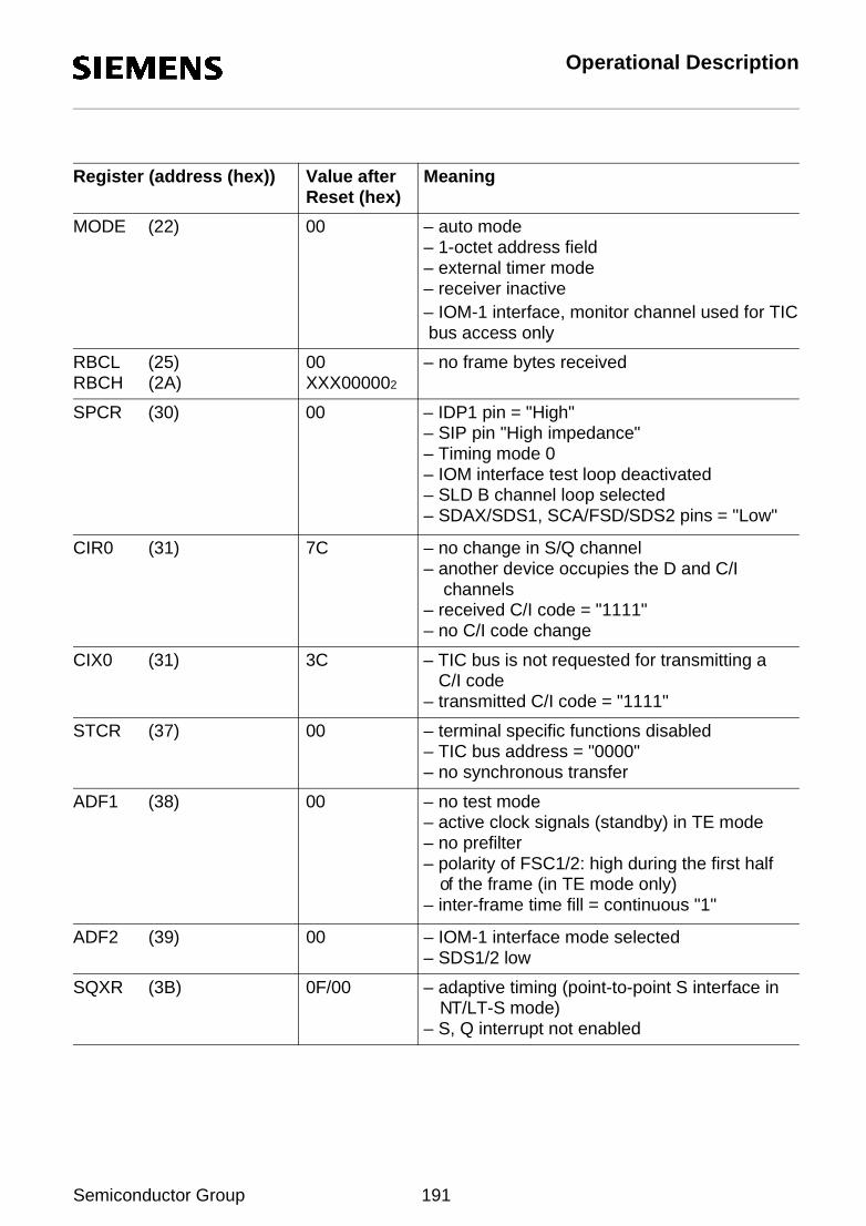
Operational Description
Value afterReset (hex)
Register (address (hex)) Meaning
MODE (22) 00 – auto mode– 1-octet address field– external timer mode– receiver inactive– IOM-1 interface, monitor channel used for TIC bus access only
RBCL (25)RBCH (2A)
00XXX000002
– no frame bytes received
SPCR (30) 00 – IDP1 pin = "High"– SIP pin "High impedance"– Timing mode 0– IOM interface test loop deactivated– SLD B channel loop selected– SDAX/SDS1, SCA/FSD/SDS2 pins = "Low"
CIR0 (31) 7C – no change in S/Q channel– another device occupies the D and C/I channels– received C/I code = "1111"– no C/I code change
CIX0 (31) 3C – TIC bus is not requested for transmitting a C/I code– transmitted C/I code = "1111"
STCR (37) 00 – terminal specific functions disabled– TIC bus address = "0000"– no synchronous transfer
ADF1 (38) 00 – no test mode– active clock signals (standby) in TE mode– no prefilter– polarity of FSC1/2: high during the first half of the frame (in TE mode only)– inter-frame time fill = continuous "1"
ADF2 (39) 00 – IOM-1 interface mode selected– SDS1/2 low
SQXR (3B) 0F/00 – adaptive timing (point-to-point S interface in NT/LT-S mode)– S, Q interrupt not enabled
Semiconductor Group 191

Operational Description
3.6 Initialization
During initialization a subset of registers have to be programmed to set the configurationparameters according to the application and desired features. They are listed in table 19.
Table 19
Register (address)
ADF2 (39H)
Bit Effect Application Restricted to
IMS
D2C2-0D1C2-0ODS
Program IOM-1 or IOM-2 interface mode
Polarity of SDS2Polarity of SDS1IOM output drivertri-state/open drain
IOM-2IOM-2IOM-2
SPCR (30H)(Note)
SPU
SAC
SPM
TLP
C2C1-0C1C1-0
Set the ISAC-S in standby by requesting clocks (if CFS = 1, register ADF1/SQXR)
SLD port inactive/active
0 Timing mode 01 Timing mode 1
0 Terminal timing mode1 Non-terminal timing mode
IOM interface test loop
B-channel switching orB/IC channel connect
TE
TE/NTLT-S/LT-T onlyTELT-S/LT-T
IOM-1
IOM-1
IOM-2
IOM-1IOM-2
SQXR (3BH) IDC
CFS
IOM Data Port IDP0,1 direction control (must be set to "0" for normal operation)
0 Permanent standby1 Power-down state enabled0 S interface point-to-point1 S-bus configuration
TE
LT-S/NT
IOM-2
IOM-2
Semiconductor Group 192

Operational Description
Register (address)
ADF1 (38H)
Bit Effect Application Restricted to
TEM
CFS
PFS
CSEL2-0
IOFFC1-2
Test Mode
0 Permanent standby1 Power down state
enabled
0 S-interface point-to-point1 S-bus configuration
Prefilter enable
IOM channel select (time slot)
IOM OFF/ONPolarity of FSC1/2
Tests with layer1 disabledTE
LT-S/NT
TE/LT-T
non-TE
TETE
IOM-1
IOM-2
IOM-2IOM-1
CIX0 (31H) RSS Hardware reset generated by either subscriber/exchange awake or watchdog timer
TE specific functions (TSF = 1)
STCR (37H) TSF
TBA2-0
Terminal specific function enable/SLD interface enable
TIC bus address Bus configuration for D + C/I (TIC)
MODE (22H) MDS2-0
TMD
DIM2-0
HDLC message transfer mode 2 bytes/1 byte address
Timer modeexternal/internal
Point-to-point/TIC bus configuration on IOM interface, for D + C/I channel arbitrationPoint-to-point/bus configuration on S/T interface, for D-channel access.
Auto mode only
Semiconductor Group 193

Operational Description
Note: After a hardware reset the pins SDAX/SDS1 and SCA/FSD/SDS2 are both "low" andhave the functions of SDS1 and SDS2 in terminal timing mode (since SPM=0), respec-tively, until the SPCR is written to for the first time. From that moment on, the functiontaken on by these pins depends on the state of the IOM Mode Select bit IMS (ADF2register).
Register (address)
TIMR (23H)
Bit Effect Application Restricted to
CNTVALUE
N1 and T1 in internal timer mode (TMD = 1)T2 in external timer mode
XAD1 (24H)XAD2 (25H)
SAPI, TEITransmit frame address
Auto mode only
SAP1/2 (26H/27H)TEI1/2 (28H/29H)
Receive SAPI, TEI address values for internal address recognition
Semiconductor Group 194

Register Description
4 Detailed Register Description
The parameterization of the ISAC-S and the transfer of data and control information betweenthe µP and ISAC-S is performed through two register sets.
The register set in the address range 00-2BH pertains to the HDLC transceiver and LAPDcontroller. It includes the two FIFOs having an identical address range from 00-1FH.
The register set ranging from 30-3BH pertains to the control of layer-1 functions and of the IOMinterface. Since the meaning of most register bits depends on the selected IOM mode (IOM-1or IOM-2), the description of this register set is divided into two sections:
4.2 Special Purpose Registers: IOM-1 Mode
4.3 Special Purpose Registers: IOM-2 Mode
The address map and a register summary are shown in the following tables:
Table 20ISAC®-S Address Map 00-2BH
Name Description
ReadAddress(hex)
Name Description
Write
RFIFO Receive FIFO00..1F
XFIFO Transmit FIFO
ISTA Interrupt Status Register20 MASK Mask Register
STAR Status Register21 CMDR Command Register
MODE Mode Register22
TIMR Timer Register23
EXIR Extended InterruptRegister
24 XAD1 Transmit Address 1
RBCL Receive Frame Byte CountLow
25 XAD2 Transmit Address 2
SAPR Received SAPI26 SAP1 Individual SAPI 1
RSTA Receive Status Register27 SAP2 Individual SAPI 2
28 TEI1 Individual TEI 1
RHCR Receive HDLC Control29 TEI2 Individual TEI 2
RBCH Receive Frame Byte CountHigh
2A
STAR2 Status Register 22B
Semiconductor Group 195

Register Description
Table 21ISAC®-S Address Map 30-3BH
Name Description
ReadAddress(hex)
Name Description
Write
SPCR Serial Port Control Register30
CIRR/CIR0
Command/IndicationReceive (0)
31 CIXR/CIX0
Command/IndicationTransmit (0)
SFCR/MOR1
SIP Feature Control Read/MONITOR Receive 1
34 SFCW/MOX1
SIP Feature Control Write/MONITOR Transmit 1
C1R Channel Register 135
MOR/MOR0
MONITOR Receive (0)32 MOX/MOX0
MONITOR Transmit (0)
SSCR/CIR1
SIP Signaling Code Receive/Command/IndicationReceive 1
33 SSCX/CIX1
SIP Signaling Code Transmit/Command/IndicationTransmit 1
C2R Channel Register 236
B1CR B1 Channel Register37 STCR Sync Transfer Control Register
B2CR B2 Channel Register38 ADF1 Additional Feature Register 1
ADF2 Additional Feature Register 239
MOSR MONITOR Status Register3A MOCR MONITOR Control Register
SQRR S, Q Channel Receive Register
3B SQXR S, Q Channel Transmit Register
Semiconductor Group 196
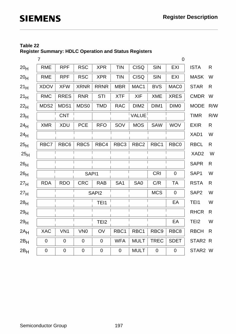
Register Description
Table 22Register Summary: HDLC Operation and Status Registers
EXISINCISQTINXPRRSCRPFRME20H
07
ISTA R
EXISINCISQTINXPRRSCRPFRME20H MASK W
MAC0BVSMAC1MBRRRNRXRNRXFWXDOV21H STAR R
XRESXMEXIFXTFSTIRNRRRESRMC21H CMDR W
DIM0DIM1DIM2RACTMDMDS0MDS1MDS222H MODE R/W
WOVSAWMOSSOVRFOPCEXDUXMR24H EXIR R
TAC/RSA0SA1RABCRCRDORDA27H RSTA R
00MULT000002BH STAR2 W
VALUE23H TIMR R/W
24H XAD1 W
RBC0RBC1RBC2RBC3RBC4RBC5RBC6RBC725H RBCL R
25H XAD2 W
29H RHCR R
RBC8RBC9RBC1RBC1OVVN0VN1XAC2AH RBCH R
26H SAPR R
0CRISAPI126H SAP1 W
0MCS27H SAP2 W
EA28H TEI1 W
29H TEI2 W
SDETTRECMULTWFA00002BH STAR2 R
CNT
SAPI2
TEI1
EATEI2
Semiconductor Group 197
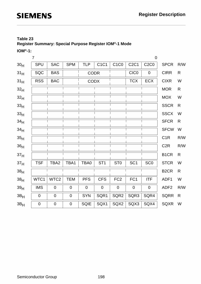
Register Description
Table 23Register Summary: Special Purpose Register IOM®-1 Mode
IOM®-1:
C2C0C2C1C1C0C1C1TLPSPMSACSPU30H
07
SPCR R/W
37H B1CR R
0CIC0CODRBASSQC31H CIRR R
ECXTCXBACRSS31H CIXR W
32H MOR R
32H MOX W
33H SSCR R
33H SSCX W
34H SFCR R
34H SFCW W
35H C1R R/W
36H C2R R/W
SC0SC1ST0ST1TBA0TBA1TBA2TSF37H STCR W
38H B2CR R
ITFFC1FC2CFSPFSTEMWTC2WTC138H ADF1 W
0000000IMS39H ADF2 R/W
SQR4SQR3SQR2SQR1SYN0003BH SQRR R
SQX4SQX3SQX2SQX1SQIE0003BH SQXR W
CODX
Semiconductor Group 198
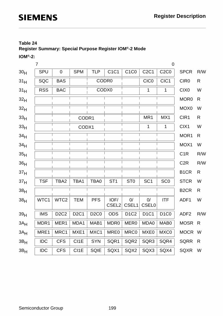
Register Description
Table 24Register Summary: Special Purpose Register IOM®-2 Mode
IOM®-2:
C2C0C2C1C1C0C1C1TLPSPM0SPU30H
07
SPCR R/W
37H B1CR R
CIC1CIC0BASSQC31H CIR0 R
11BACRSS31H CIX0 W
32H MOR0 R
32H MOX0 W
MAB0MDA0MER0MDR0MAB1MDA1MER1MDR13AH MOSR R
MXC0MXE0MRC0MRE0MXC1MXE1MRC1MRE13AH MOCR W
35H C1R R/W
36H C2R R/W
SC0SC1ST0ST1TBA0TBA1TBA2TSF37H STCR W
38H B2CR R
D1C0D1C1D1C2ODSD2C0D2C1D2C2IMS39H ADF2 R/W
SQR4SQR3SQR2SQR1SYNCI1ECFSIDC3BH SQRR R
SQX4SQX3SQX2SQX1SQIECI1ECFSIDC3BH SQXR W
MX1MR133H CIR1 R
1133H CIX1 W
34H MOR1 R
34H MOX1 W
ITF0/CSEL0
0/CSEL1
IOF/CSEL2
PFSTEMWTC2WTC138H ADF1 W
CODR0
CODX0
CODR1
CODX1
Semiconductor Group 199

Register Description
4.1 HDLC Operation and Status Registers
4.1.1 Receive FIFO RFIFO Read Address 00-1FH
A read access to any address within the range 00-1FH gives access to the "current" FIFOlocation selected by an internal pointer which is automatically incremented after each readaccess. This allows for the use of efficient ’move string’ type commands by the processor.
The RFIFO contains up to 32 bytes of received frame.
After an ISTA:RPF interrupt, exactly 32 bytes are available.
After an ISTA:RME interrupt, the number of bytes available can be obtained by reading theRBCL register.
4.1.2 Transmit FIFO XFIFO Write Address 00-1FH
A write access to any address within the range 00-1FH gives access to the "current" FIFOlocation selected by an internal pointer which is automatically incremented after each writeaccess. This allows for the use of efficient ’move string’ type commands by the processor.
Up to 32 bytes of transmit data can be written into the XFIFO following an ISTA:XPR interrupt.
4.1.3 Interrupt Status Register ISTA Read Address 20H
Value after reset: 00H
RME Receive Message End
One complete frame of length less than or equal to 32 bytes, or the last part of a frameof length greater than 32 bytes has been received. The contents are available in theRFIFO. The message length and additional information may be obtained fromRBCH + RBCL and the RSTA register.
RPF Receive Pool Full
A 32-byte block of a frame longer than 32 bytes has been received and is availablein the RFIFO. The frame is not yet complete.
RSC Receive Status Change. Used in auto-mode only.
A status change in the receiver of the remote station – Receiver Ready/Receiver NotReady – has been detected (RR or RNR S-frame).
The actual status of the remote station can be read from the STAR register (RRNRbit).
EXISINCISQTINXPRRSCRPFRME
07
Semiconductor Group 200

Register Description
XPR Transmit Pool Ready
A data block of up to 32 bytes can be written to the XFIFO.
An XPR interrupt will be generated in the following cases:
– after an XTF or XIF command, when one transmit pool is emptied and the frame isnot yet complete
– after an XTF together with an XME command is issued, when the wholetransparent frame has been transmitted
– after an XIF together with an XME command is issued, when the whole I-frame hasbeen transmitted and a positive acknowledgement from the remote station hasbeen received, (auto-mode).
TIN Timer InterruptThe internal timer and repeat counter has expired (see TIMR register).
CISQ C/I or S/Q Channel ChangeA change in C/I channel 0, C/I channel 1 (only in IOM-2 TE mode) or S/Q channel hasbeen recognized. The actual value can be read from CIR0, CIR1 or SQRR.
SIN Synchronous Transfer Interrupt
When programmed (STCR register), this interrupt is generated to enable theprocessor to lock on to the IOM timing, for synchronous transfers.
EXI Extended Interrupt
This bit indicates that one of six non-critical interrupts has been generated. The exactinterrupt cause can be read from EXIR.
Note: A read of the ISTA register clears all bits except EXI and CISQ. EXI is cleared byreading the EXIR register, CISQ is cleared by reading CIRR/CIR0.
4.1.4 Mask Register MASK Write Address 20H
Value after reset: 00H
Each interrupt source in the ISTA register can be selectively masked by setting to "1"the corresponding bit in MASK. Masked interrupt status bits are not indicated whenISTA is read. Instead, they remain internally stored and pending, until the mask bit isreset to zero.
Note: In the event of an extended interrupt and of a C/I or S/Q channel change, EXI andCISQ are set in ISTA even if the corresponding mask bits in MASK are active, but nointerrupt (INT pin) is generated.
4.1.5 Status Register STAR Read Address 21H
07
EXISINCISQTINXPRRSCRPFRME
Semiconductor Group 201

Register Description
Value after reset: 48H
XDOV Transmit Data Overflow
More than 32 bytes have been written in one pool of the XFIFO, i.e. data has beenoverwritten.
XFW Transmit FIFO Write Enable
Data can be written in the XFIFO. This bit may be polled instead of (or in addition to)using the XPR interrupt.
XRNR Transmit RNR. Used in auto-mode only
In auto-mode, this bit indicates whether the ISAC-S receiver is in the "ready" (0) or"not ready" (1) state. When "not ready", the ISAC-S sends an RNR S-frameautonomously to the remote station when an I-frame or an S-frame is received.
RRNR Receive RNR. Used in auto-mode only
In the auto-mode, this bit indicates whether the ISAC-S has received an RR or anRNR frame, this being an indication of the current state of the remote station: receiverready (0) or receiver not ready (1).
MBR Message Buffer Ready
This bit signifies that temporary storage is available in the RFIFO to receive at leastthe first 16 bytes of a new message.
MAC1 MONITOR Transmit Channel 1 Active (IOM-2 terminal mode only)
Data transmission is in progress in MONITOR channel 1.
BVS B-channel valid on SIP (IOM-1 mode only). B channel on SIP (SLD) can be accessed.
MAC0 MONITOR Transmit Channel 0 Active. Used in IOM-2 mode only.
Data transmission is in progress in MONITOR channel 0.
07
MAC0BVSMAC1MBRRRNRXRNRXFWXDOV
Semiconductor Group 202

Register Description
4.1.6 Command Register CMDR Write Address 21H
Value after reset: 00H
Note: The maximum time between writing to the CMDR register and the execution of thecommand is 2.5 DCL clock cycles. During this time no further commands should bewritten to the CMDR register to avoid any loss of commands.
RMC Receive Message Complete
Reaction to RPF (Receive Pool Full) or RME (Receive Message End) interrupt. Bysetting this bit, the processor confirms that it has fetched the data, and indicates thatthe corresponding space in the RFIFO may be released.
RRES Receiver Reset
HDLC receiver is reset, the RFIFO is cleared of any data.
In addition, in auto-mode, the transmit and receive counters (V(S), V(R)) are reset
RNR Receiver Not ReadyUsed in auto-mode only.
Determines the state of the ISAC-S HDLC receiver.
When RNR = "0", a received I or S-frame is acknowledged by an RR supervisoryframe, otherwise by an RNR supervisory frame.
STI Start Timer
The ISAC-S hardware timer is started when STI is set to one. In the internal timermode (TMD bit, MODE register) an S-Command (RR, RNR) with poll bit set istransmitted in addition. The timer may be stopped by a write of the TIMR register.
XTF Transmit Transparent Frame
After having written up to 32 bytes in the XFIFO, the processor initiates thetransmission of a transparent frame by setting this bit to "1". The opening flag isautomatically added to the message by the ISAC-S.
XIF Transmit I-Frame Used in auto-mode only
After having written up to 32 bytes in the XFIFO, the processor initiates thetransmission of an I-frame by setting this bit to "1". The opening flag, the address andthe control field are automatically added by the ISAC-S.
07
XRESXMEXIFXTFSTIRNRRRESRMC
Semiconductor Group 203

Register Description
XME Transmit Message End
By setting this bit to "1" the processor indicates that the data block written last in theXFIFO completes the corresponding frame. The ISAC-S terminates the transmissionby appending the CRC and the closing flag sequence to the data.
XRES Transmitter Reset
HDLC transmitter is reset and the XFIFO is cleared of any data.
This command can be used by the processor to abort a frame currently intransmission.
Notes: After an XPR interrupt further data has to be written in the XFIFO and theappropriate Transmit Command (XTF or XIF) has to be written in the CMDRregister again to continue transmission, when the current frame is not yet complete(see also XPR in ISTA).
During frame transmission, the 0-bit insertion according to the HDLC bit-stuffingmechanism is done automatically.
4.1.7 Mode Register MODE Read/Write Address 22H
Value after reset: 00H
MDS2-0 Mode Select
Determines the message transfer mode of the HDLC controller, as follows:
07
DIM0DIM1DIM2RACTMDMDS0MDS1MDS2
Semiconductor Group 204

Register Description
Note: SAP1, SAP2: two programmable address values for the first received address byte(in the case of an address field longer than 1 byte); SAPG = fixed value FC/FEH.
TEI1, TEI2: two programmable address values for the second (or the only, in the caseof a one-byte address) received address byte; TEIG = fixed value FFH.
TMD Timer Mode
Sets the operating mode of the ISAC-S timer. In the external mode (0) the timer iscontrolled by the processor. It is started by setting the STI bit in CMDR and it isstopped by a write of the TIMR register.
In the internal mode (1) the timer is used internally by ISAC-S for timeout and retryconditions (handling of LAPD/HDLC protocol in auto-mode).
MDS2MDS1MDS0
Addresss Comparison1. Byte 2. Byte
Remark
0 0 0 TEI1, TEI2 – One-byte address compare. HDLC protocolhandling for frames withaddress TEI1
Mode
Auto-mode
NumberofAddressBytes
1
0 0 1 SAP1, SAP2, SAPG TEI1, TEI2, TEIG Two-byte address compare. LAPD protocolhandling for frames withaddress SAP1 + TEI1
Auto-mode 2
0 1 0 TEI1, TEI2 – One-byte address compare.
Non-auto-mode
1
0 1 1 SAP1, SAP2, SAPG TEI1, TEI2, TEIG Two-byte address compare.
Non-auto-mode
2
1 0 0 Reserved
1 0 1 – TEI1, TEI2, TEIG Low-byte address compare.
Transparent mode 1
>1
1 1 0 – – No address compare.All frames accepted.
Transparent mode 2
–
1 1 1 SAP1, SAP2, SAPG – High-byte address compare.
Transparent mode 3
>1
Semiconductor Group 205
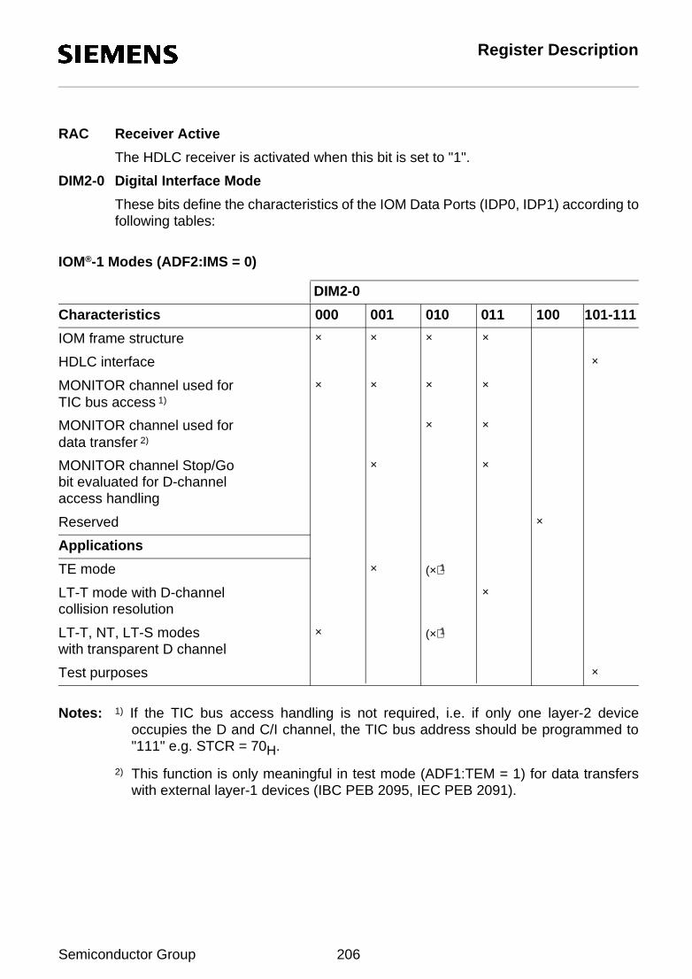
Register Description
RAC Receiver Active
The HDLC receiver is activated when this bit is set to "1".
DIM2-0 Digital Interface Mode
These bits define the characteristics of the IOM Data Ports (IDP0, IDP1) according tofollowing tables:
IOM®-1 Modes (ADF2:IMS = 0)
Notes: 1) If the TIC bus access handling is not required, i.e. if only one layer-2 deviceoccupies the D and C/I channel, the TIC bus address should be programmed to"111" e.g. STCR = 70H.
2) This function is only meaningful in test mode (ADF1:TEM = 1) for data transferswith external layer-1 devices (IBC PEB 2095, IEC PEB 2091).
000Characteristics 001
×IOM frame structure × × ×
010 100 101-111011
DIM2-0
Test purposes ×
HDLC interface ×
×MONITOR channel used for TIC bus access 1)
× × ×
MONITOR channel used for data transfer 2)
× ×
MONITOR channel Stop/Go bit evaluated for D-channel access handling
× ×
Reserved ×
Applications
TE mode × (×)1
LT-T mode with D-channel collision resolution
×
×LT-T, NT, LT-S modes with transparent D channel
(×)1
Semiconductor Group 206

Register Description
IOM®-2 Modes (ADF2:IMS = 1)
4.1.8 Timer Register TIMR Read/Write Address 23H
Value after reset: undefined (previous value)
CNT The meaning depends on the selected timer mode (TMD bit, MODE register).
* internal Timer Mode (TMD = 1)
CNT indicates the maximum number of S-commands "N1" which are transmittedautonomously by the ISAC-S after expiration of time period T1 (retry, according toHDLC).
Characteristics
×IOM-2 terminal mode SPCR:SPM = 0
× × ×
100-111
IOM-2 non-terminal mode SPCR:SPM = 1
× ×
×Last octet of IOM channel 2 used for TIC bus access
×
Stop/Go bit evaluated for D-channel access handling
× ×
Reserved
Applications
TE mode
LT-T mode with D-channel collision resolution
LT-T, NT, LT-S modes with transparent D channel
000 001 010 011
×
× ×
×
×
07
DIM2-0
VALUECNT
Semiconductor Group 207

Register Description
The internal timer procedure will be started in auto-mode:
– after start of an I-frame transmission
or
– after an "RNR" S-frame has been received.
After the last retry, a timer interrupt (TIN-bit in ISTA) is generated.
The timer procedure will be stopped when
– a TIN interrupt is generated. The time between the start of an I-frametransmission or reception of an "RNR" S-frame and the generation of a TINinterrupt is equal to: (CNT+1) × T1.
– or the TIMR is written
– or a positive or negative acknowledgement has been received.
Note: The maximum value of CNT can be 6. If CNT is set to 7, the number of retriesis unlimited.
* External Timer Mode (TMD = 0)
CNT together with VALUE determine the time period T2 after which a TIN interruptwill be generated:
CNT × 2.048 s + T1
with T1 = (VALUE + 1) × 0.064 s,
in the normal case, and
T2 = 16348 × CNT × DCL + T1
with T1 = 512 × (VALUE + 1) × DCL
when TLP = 1 (test loop activated, SPCR register).
DCL denotes the period of the DCL clock.
The timer can be started by setting the STI-bit in CMDR and will be stopped when aTIN interrupt is generated or the TIMR register is written.
Note: If CNT is set to 7, a TIN interrupt is indefinitely generated after everyexpiration of T1.
VALUE Determines the Time Period T1:
T1 = (VALUE + 1) × 0.064 s (SPCR:TLP = 0, normal mode)
T1 = 512 × (VALUE + 1) × DCL (SPCR:TLP = 1, test mode).
Semiconductor Group 208
Register Description
4.1.9 Extended Interrupt Register EXIR Read Address 24H
Value after reset: 00H
XMR Transmit Message Repeat
The transmission of the last frame has to be repeated because:
– the ISAC-S has received a negative acknowledgement to an I-frame in auto-mode(according to HDLC/LAPD)
– or a collision on the S-bus has been detected after the 32nd data byte of a transmitframe.
XDU Transmit Data Underrun
The current transmission of a frame is aborted by transmitting seven "1's" becausethe XFIFO holds no further data. This interrupt occurs whenever the processor hasfailed to respond to an XPR interrupt (ISTA register) quickly enough, after havinginitiated a transmission and the message to be transmitted is not yet complete.
Note: When an XMR or and XDU interrupt is generated, it is not possible to sendtransparent frames or I-frames until the interrupt has been acknowledged by readingEXIR.
PCE Protocol Error Used in auto-mode only.
A protocol error has been detected in auto-mode due to a received
– S- or I-frame with an incorrect sequence number N(R) or
– S-frame containing an I-field.
– I-frame which is not a command.
– S-frame with an undefined control field.
RFO Receive Frame Overflow
The received data of a frame could not be stored, because the RFIFO is occupied.The whole message is lost.
This interrupt can be used for statistical purposes and indicates that the processordoes not respond quickly enough to an RPF or RME interrupt (ISTA).
SOV Synchronous Transfer Overflow
The synchronous transfer programmed in STCR has not been acknowledged in timevia the SC0/SC1 bit.
MOS MONITOR Status
A change in the MONITOR Status Register (MOSR) has occured (IOM-2).
A new MONITOR channel byte is stored in MOR (IOM-1).
07
WOVSAWMOSSOVRFOPCEXDUXMR
Semiconductor Group 209

Register Description
SAW Subscriber Awake Used only if terminal specific functions are enabled (STCR:TSF = 1).
Indicates that a falling edge on the EAW line has been detected, in case the terminalspecific functions are enabled (TSF-bit in STCR).
WOV Watchdog Timer Overflow Used only if terminal specific functions are enabled (STCR:TSF = 1).
Signals the expiration of the watchdog timer, which means that the processor hasfailed to set the watchdog timer control bits WTC1 and WTC2 (ADF1 register) in thecorrect manner. A reset pulse has been generated by the ISAC-S.
4.1.10 Transmit Address 1 XAD1 Write Address 24H
Used in auto-mode only.
XAD1 contains a programmable address byte which is appended automatically to theframe by the ISAC-S in auto-mode. Depending on the selected address mode XAD1is interpreted as follows:
* 2-Byte Address Field
XAD1 is the high byte (SAPI in the ISDN) of the 2-byte address field. Bit 1 isinterpreted as the command/response bit "C/R". It is automatically generated by theISAC-S following the rules of ISDN LAPD protocol and the CRI bit value in SAP1register. Bit 1 has to be set to "0".
In the ISDN LAPD the address field extension bit "EA", i.e. bit 0 of XAD1 has to beset to "0".
* 1-Byte Address Field
According to the X.25 LAPB protocol, XAD1 is the address of a command frame.
Note: In standard ISDN applications only 2-byte address fields are used.
C/R Bit
Command Response Transmitting End CRI Bit
0 1 subscriber 0
1 0 network 1
07
Semiconductor Group 210

Register Description
4.1.11 Receive Frame Byte Count Low RBCL Read Address 25H
Value after reset: 00H
RBC7-0 Receive Byte Count
Eight least significant bits of the total number of bytes in a received message. BitsRBC4-0 indicate the length of the data block currently available in the RFIFO, theother bits (together with RBCH) indicate the number of whole 32-byte blocksreceived.
If exactly 32 bytes are received RBCL holds the value 20H.
4.1.12 Transmit Address 2 XAD2 Write Address 25H
Used in auto-mode only.
XAD2 contains the second programmable address byte, whose function depends onthe selected address mode:
* 2-Byte Address Field
XAD2 is the low byte (TEI in the ISDN) of the 2-byte address field.
* 1-Byte Address Field
According to the X.25 LAPB protocol, XAD2 is the address of a response frame.
Note: See note to XAD1 register description.
4.1.13 Received SAPI Register SAPR Read Address 26H
When transparent mode 1 is selected, SAPR contains the value of the first addressbyte of a receive frame.
07
RBC0RBC1RBC2RBC3RBC4RBC5RBC6RBC7
07
07
Semiconductor Group 211

Register Description
4.1.14 SAPI1 Register SAP1 Write Address 26H
SAPI1 SAPI1 Value
Value of the first programmable Service Access Point Identifier (SAPI) according tothe ISDN LAPD protocol.
CRI Command/Response Interpretation
CRI defines the end of the ISDN user-network interface the ISAC-S is used on, forthe correct identification of "Command" and "Response" frames. Depending on thevalue of CRI the C/R-bit will be interpreted by the ISAC-S, when receiving frames inauto-mode, as follows:
For transmitting frames in auto-mode, the C/R-bit manipulation will also be doneautomatically, depending on the value of the CRI-bit (refer to XAD1 registerdescription).
In message transfer modes with SAPI address recognition the first received addressbyte is compared with the programmable values in SAP1, SAP2 and the fixed groupSAPI.
In 1-byte address mode, the CRI-bit is to be set to "0".
4.1.15 Receive Status Register RSTA Read Address 27H
Value after reset: undefined
RDA Receive Data
A "1" indicates that data is available in the RFIFO. After an RME interrupt, a "0" in thisbit means that data is available in the internal registers RHCR or SAPR only (e.g.S-frame). See also RHCR register description table.
RDO Receive Data Overflow
At least one byte of the frame has been lost, because it could not be stored in RFIFO(1).
C/R Bit
Command Receiving End Command Response
0 subscriber 1 0
1 network 0 1
07
0CRISAPI1
07
TAC/RSA0SA1RABCRCRDORDA
Semiconductor Group 212

Register Description
CRC CRC Check
The CRC is correct (1) or incorrect (0).
RAB Receive Message Aborted
The receive message was aborted by the remote station (1), i.e. a sequence of 7 1’swas detected.
SA1-0 SAPI Address Identification
TA TEI Address Identification
SA1-0 are significant in auto-mode and non-auto-mode with a two-byte address field,as well as in transparent mode 3. TA is significant in all modes except in transparentmodes 2 and 3.
Two programmable SAPI values (SAP1, SAP2) plus a fixed group SAPI (SAPG ofvalue FC/FEH), and two programmable TEI values (TEI1, TEI2) plus a fixed groupTEI (TEIG of value FFH), are available for address comparison.
The result of the address comparison is given by SA1-0 and TA, as follows
Notes: If the SAPI values programmed to SAP1 and SAP2 are identical the reception of aframe with SAP2/TEI2 results in the indication SA1 = 1, SA0 = 0, TA = 1.
Normally RSTA should be read by the processor after an RME interrupt in order todetermine the status of the received frame. The contents of RSTA are valid onlyafter an RME interrupt, and remain so until the frame is acknowledged via the RMCbit.
SA1 SA0 TA 1st Byte 2nd Byte
Address Match with
xx
Number of addressbytes = 1
xx
01
TEI2TEI1
––
0000111
Number of addressbytes = 2
0011001
010101x
SAP2SAP2SAPGSAPGSAP1SAP1
reserved
TEIGTEI2TEIGTEI1 or TEI2TEIGTEI1
Semiconductor Group 213
Register Description
SAPI1
C/R Command/Response
The C/R bit identifies a receive frame as either a command or a response, accordingto the LAPD rules:
4.1.16 SAPI2 Register SAP2 Write Address 27H
SAPI2 SAPI2 Value
Value of the second programmable Service Access Point Identifier (SAPI) accordingto the ISDN LAPD protocol.
MCS Modulo Count Select Used in auto-mode only.
This bit determines the HDLC control field format as follows:
0: One-byte control field (modulo 8)
1: Two-byte control field (modulo 128)
4.1.17 TEI1 Register 1 TEI1 Write Address 28H
EA Address field Extension Bit
This bit has to be set "1" according to HDLC/LAPD.
In all message transfer modes except in transparent modes 2 and 3, TEI1 is used bythe ISAC-S for address recognition. In the case of a two-byte address field, it containsthe value of the first programmable Terminal Endpoint Identifier according to theISDN LAPD protocol.
In the auto-mode with a two-byte address field, numbered frames with the addressSAPI1-TEI1 are handled autonomously by the ISAC-S according to the LAPDprotocol.
Command Response Direction
0 1 Subscriber to network
1 0 Network to subscriber
07
0MCSSAPI2
07
EATEI1
Semiconductor Group 214

Register Description
Note: If the value FFH is programmed in TEI1, received numbered frames with addressSAPI1-TEI1 (SAPI1-TEIG) are not handled autonomously by the ISAC-S.
In auto and non-auto-modes with one-byte address field, TEI1 is a commandaddress, according to X.25 LAPB.
4.1.18 Receive HDLC Control Register RHCR Read Address 29H
In all modes except transparent modes 2 and 3, this register contains the control field of areceived HDLC frame. In transparent modes 2 and 3, the register is not used.
Mode Modulo 8 (MCS = 0)
Modulo 128 (MCS = 1)
Contents of RFIFO
Auto-mode,1-byte address(U/I frames)
(Note 1)
Control field U-frames only:Control field
(Note 2)
From 3rd byte after flag(Note 4)
Auto-mode,1-byte address(I frames)
Control field incompressed form
(Note 3)
From 4th byte after flag(Note 4)
Auto-mode,2-byte address(U/I frames)
(Note 1)
Control field U-frames only:Control field
(Note 2)
From 4th byte after flag(Note 4)
Auto-mode,2-byte address(I frames)
Control field incompressed form
(Note 3)
From 5th byte after flag(Note 4)
Non-auto-mode,1-byte address
2nd byte after flag From 3rd byte after flag
Non-auto-mode,2-byte address
3rd byte after flag From 4th byte after flag
Transparent mode 1 3rd byte after flag From 4th byte after flag
Transparent mode 2 – From 1st byte after flag
Transparent mode 3 – From 2nd byte after flag
Contents of RHCR
07
Semiconductor Group 215

Register Description
Note 1: S frames are handled automatically and are not transferred to the microprocessor.
Note 2: For U frames (bit 0 of RHCR = 1) the control field is as in the modulo 8 case.
Note 3: For I frames (bit 0 of RHCR = 0) the compressed control field has the same formatas in the modulo 8 case, but only the three LSB’s of the receive and transmit countersare visible:
Note 4: I-field.
4.1.19 TEI2 Register TEI2 Write Address 29H
EA Address Field Extension Bit
This bit is to be set to "1" according to HDLC/LAPD.
In all message transfer modes except in transparent modes 2 and 3, TEI2 is used by the ISAC-S for address recognition. In the case of a two-byte address field, it contains the value of thesecond programmable Terminal Endpoint Identifier according of the ISDN LAPD protocol.
In auto and non-auto-modes with one-byte address field, TEI2 is a response address,according to X.25 LAPB.
4.1.20 Receive Frame Byte Count High RBCH Read Address 2AH
Value after reset: 0XX000002.
XAC Transmitter Active
The HDLC transmitter is active when XAC = 1. This bit may be polled. The XAC bit isactive when
– either an XTF/XIF command is issued and the frame has not been completelytransmitted
– or the transmission of an S frame is internally initiated and not yet completed.
0PN(R)2-0 N(S)2-0
07
07
EATEI2
07
RBC8RBC9RBC10RBC11OVVN0VN1XAC
Semiconductor Group 216

Register Description
VN1-0 Version Number of Chip
PEB 2085 PEB 2086
0 ... A1 to A2 version 0 ... V1.11 ... B1 version2 ... B2 version3 ... V2.3 (B3) version
OV Overflow
A "1" in this bit position indicates a message longer than 4095 bytes.
RBC8-11Receive Byte Count
Four most significant bits of the total number of bytes in a received message.
Note: Normally RBCH and RBCL should be read by the processor after an RME interruptin order to determine the number of bytes to be read from the RFIFO, and the totalmessage length. The contents of the registers are valid only after an RME interrupt,and remain so until the frame is acknowledged via the RMC bit.
4.1.21 Status Register 2 STAR2 Read/Write Address 2BH
Value after reset: 00H
a) WRITE
MULT Used in NT/LT-S modes to enable or disable the multiframe structure (seechapter 2.5.1.9)
1: S/T multiframe disabled0: S/T multiframe enabled
b) READ
WFA Waiting for Acknowledge This bit shows, if the last transmitted I-frame was acknowledged, i.e. V(A) = V(S)(⇒ WFA = 0) or was not yet acknowledged, i.e. V(A) < V(S) (⇒ WFA = 1).
MULT The value written into the register bit is read.
TREC Timer Recovery Status:
0: The device is not in the Timer Recovery state.1: The device is in the Timer Recovery state.
07
00MULT00000
07
SDETTRECMULTWFA0000
Semiconductor Group 217

Register Description
SDET S-Frame Detected: This bit is set to "1" by the first received correct I-frame or S-command with p = 1. Itis reset by reading STAR2 or by a Hardware Reset.
Semiconductor Group 218

Register Description
4.2 Special Purpose Registers: IOM®-1 Mode
The following register description is only valid if IOM-1 mode is selected (ADF2:IMS = 0).
For IOM-2 mode refer to chapter 4.3.
4.2.1 Serial Port Control Register SPCR Read/Write Address 30H
Value after reset: 00H
Important Note After a hardware reset the pins SDAX/SDS1 and SCA/FSD/SDS2 are both"low" and have the functions of SDS1 and SDS2 in terminal timing mode(since SPM = 0), respectively, until the SPCR is written to for the first time.From that moment on, the function taken on by these pins depends on thestate of the IOM Mode Select bit IMS (ADF2 register).
SPU Software Power Up Used in TE mode only.
If ADF1:CFS=1, before activating the ISDN S-interface in TE mode the SPU-bit hasto be set to "1" and then cleared again:
After a subsequent CISQ interrupt (C/I code change; ISTA) and reception of the C/Icode "PU" (Power Up indication in TE mode) the reaction of the processor would be:
– to write an Activate Request command as C/I code in the CIXR register.
– to reset the SPU-bit and wait for the following CISQ interrupt.
SAC SIP Port Activation SIP port is in high impedance state (SAC = 0) or operating (SAC = 1).
SPM Serial Port Timing Mode Depending on the interface mode, the following timing options are provided.
0: Timing mode 0; SIP (SLD) operates in master mode, SCA supplies the 128-kHz data clock signal for port A (SSI).typical applications: TE, NT modes
1: Timing mode 1; SIP (SLD) operates in slave mode, FSD supplies a delayed frame synchronization signal for the IOM interface, serial port A (SSI) is notused.typical applications: LT-T, LT-S modes
07
C2C0C2C1C1C0C1C1TLPSPMSACSPU
Semiconductor Group 219
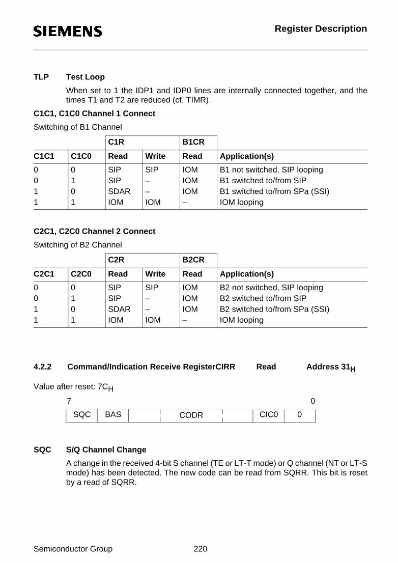
Register Description
TLP Test Loop
When set to 1 the IDP1 and IDP0 lines are internally connected together, and thetimes T1 and T2 are reduced (cf. TIMR).
C1C1, C1C0 Channel 1 Connect
Switching of B1 Channel
C2C1, C2C0 Channel 2 Connect
Switching of B2 Channel
4.2.2 Command/Indication Receive RegisterCIRR Read Address 31H
Value after reset: 7CH
SQC S/Q Channel Change
A change in the received 4-bit S channel (TE or LT-T mode) or Q channel (NT or LT-Smode) has been detected. The new code can be read from SQRR. This bit is resetby a read of SQRR.
C1C1 Application(s)C1C0 Read Write Read
0 B1 not switched, SIP looping0 SIP SIP IOM0 B1 switched to/from SIP1 SIP – IOM1 B1 switched to/from SPa (SSI)0 SDAR – IOM1 IOM looping1 IOM IOM –
C1R B1CR
C2C1 Application(s)C2C0 Read Write Read
0 B2 not switched, SIP looping0 SIP SIP IOM0 B2 switched to/from SIP1 SIP – IOM1 B2 switched to/from SPa (SSI)0 SDAR – IOM1 IOM looping1 IOM IOM –
C2R B2CR
07
0CIC0BASSQC CODR
Semiconductor Group 220

Register Description
BAS Bus Access Status
Indicates the state of the TIC-bus:
0: the ISAC-S itself occupies the D and C/I channel1: another device occupies the D and C/I channel
CODR C/I Code Receive
Value of the received Command/Indication code. A C/I code is loaded in CODR onlyafter being the same in two consecutive IOM frames and the previous code has beenread from CIRR.
(refer to chapter 3.3.2)
CIC0 C/I Code Change
A change in the received Command/Indication code has been recognized. This bit isset only when a new code is detected in two consecutive IOM frames. It is reset by aread of CIRR.
Note: The BAS and CODR bits are updated every time a new C/I code is detected in twoconsecutive IOM frames.
If several consecutive codes are detected and CIRR is not read, only the first and thelast C/I code (and BAS bit) is made available in CIRR at the first and second read ofthat register, respectively.
4.2.3 Command/Indication Transmit RegisterCIXR Write Address 31H
Value after reset: 3CH
RSS Reset Source Select
Only valid if the terminal specific functions are activated (STCR:TSF).
0 : Subscriber or Exchange Awake
As reset source serves:
– a falling edge on the EAW line (External Subscriber Awake)
– a C/I code change (Exchange Awake).
A logical zero on the EAW line activates also the IOM-interface clock and framesignal, just as the SPU-bit (SPCR) does.
07
ECXTCXBACRSS CODX
Semiconductor Group 221

Register Description
1: Watchdog Timer
The expiration of the watchdog timer generates a reset pulse.
The watchdog timer will be reset and restarted, when two specific bitcombinations are written in the ADF1 register within the time period of 128 ms(see also ADF1 register description).
After a reset pulse generated by the ISAC-S and the corresponding interrupt(WOV, SAW or CISQ) the actual reset source can be read from the ISTA andEXIR register.
BAC Bus Access Control
Only valid if the TIC-bus feature is enabled (MODE:DIM2-0).
If this bit is set, the ISAC-S will try to access the TIC-bus to occupy the C/I channeleven if no D channel frame has to be transmitted. It should be reset when the accesshas been completed to grant a similar access to other devices transmitting in that IOMchannel.
Note: Access is always granted by default to the ISAC-S/ICC with TIC bus address (TBA2-0, STCR register) "7", which is the lowest priority in a bus configuration.
CODX C/I Code Transmit
Code to be transmitted in the C/I channel (refer to chapter 3.3.2).
TCX T-Channel Transmit
Output on IOM in T channel.
ECX E-Channel Transmit
Output on IOM in E channel.
4.2.4 MONITOR Receive Register MOR Read Address 32H
Contains the MONITOR data received according to the MONITOR channel protocol(E bit = 0).
4.2.5 MONITOR Transmit Register MOX Write Address 32H
The byte written into MOX is transmitted once in the MONITOR channel.
07
07
Semiconductor Group 222

Register Description
4.2.6 SIP Signaling Code Receive SSCR Read Address 33H
Value after reset: FFH
Only valid in timing mode 0 (SPCR:SPM = 0).
The signaling byte received on SIP can be read from this register.
4.2.7 SIP Signaling Code Transmit SSCX Write Address 33H
Value after reset: FFH
Significant only in timing mode 0 (SPCR:SPM = 0).
The contents of SSCX are continuously output in the signaling byte on SIP (SLD).
4.2.8 SIP Feature Control Read SFCR Read Address 34H
Contains the FC data received on SIP (timing mode 0 only, SPCR:SPM = 0).
4.2.9 SIP Feature Control Write SFCW Write Address 34H
The byte written into SFCW is output once on SIP in the FC channel (timing mode 0only, SPCR:SPM = 0).
07
07
07
07
Semiconductor Group 223

Register Description
4.2.10 Channel Register 1 C1R Read/Write Address 35H
Contains the value received/transmitted in the B1 channel (see C1C1, C1C0, SPCRregister).
4.2.11 Channel Register 2 C2R Read/Write Address 36H
Contains the value received/transmitted in the B2 channel (see C2C1, C2C0, SPCRregister).
4.2.12 B1 Channel Register B1CR Read Address 37H
Contains the value received in the B1 channel, as programmed (see C1C1, C1C0,SPCR register).
4.2.13 Synchronous Transfer Control RegisterSTCR Write Address 37H
Value after reset: 00H
TSF Terminal Specific Functions
0: No terminal specific functions
1: The terminal specific functions are activated, such as
– Watchdog Timer
– Subscriber/Exchange Awake (SIP/EAW).
In this case the SIP/EAW line is always an input signal which can serve as arequest signal from the subscriber to initiate the awake function in a terminal.
07
07
07
07
SC0SC1ST0ST1TBA0TBA1TBA2TSF
Semiconductor Group 224

Register Description
A falling edge on the EAW line generates an SAW interrupt (EXIR).
When the RSS-bit in the CIXR register is zero, a falling edge on the EAW line(Subscriber Awake) or a C/I code change (Exchange Awake) initiates a resetpulse.
When the RSS-bit is set to one a reset pulse is triggered only by the expirationof the watchdog timer (see also CIXR register description).
Note: The TSF-bit will be cleared only by hardware reset.
TBA2-0 TIC Bus Address
Defines the individual address for the ISAC-S on the IOM TIC bus(see chapter 2.3.9).
This address is used to access the C/I and D channel on the IOM.
Note: One device liable to transmit in C/I and D fields on IOM should always be given theaddress value "7".
ST1 Synchronous Transfer 1
When set, causes the ISAC-S to generate an SIN interrupt status (ISTA register) atthe beginning of an IOM frame.
ST0 Synchronous Transfer 0
When set, causes the ISAC-S to generate an SIN interrupt status (ISTA register) atthe middle of an IOM frame.
SC1 Synchronous Transfer 1 Completed
After an SIN interrupt the processor has to acknowledge the interrupt by setting theSC1-bit before the middle of the IOM frame, if the interrupt was originated from aSynchronous Transfer 1 (ST1).
Otherwise an SOV interrupt (EXIR register) will be generated.
SC0 Synchronous Transfer 0 Completed
After an SIN interrupt the processor has to acknowledge the interrupt by setting theSC0-bit before the start of the next IOM frame, if the interrupt was originated from aSynchronous Transfer 0 (ST0).
Otherwise an SOV interrupt (EXIR register) will be generated.
Note: ST0/1 and SC0/1 are useful for synchronizing MP accesses andreceive/transmit operations.
Semiconductor Group 225

Register Description
4.2.14 B2 Channel Register B2CR Read Address 38H
Contains the value received in the B2 channel, as programmed(see C2C1, C2C0, SPCR register).
4.2.15 Additional Feature Register 1 ADF1 Write Address 38H
Value after reset: 00H
WTC1, 2 Watchdog Timer Control 1, 2
After the watchdog timer mode has been selected (STCR:TSF = CIXR:RSS = 1) thewatchdog timer is started.
During every time period of 128 ms the processor has to program the WTC1- andWTC2-bit in the following sequence:
to reset and restart the watchdog timer.
If not, the timer expires and a WOV interrupt (EXIR) together with a reset pulse is ge-nerated.
TEM Test Mode
In Test mode (TEM = 1, PFS = 0) all layer-1 functions are disabled and the ISAC-Sbehaves like an ICC (PEB 2070) device.
PFS Prefilter Select
These bits together determine the pre-filter delay compensation and the test mode(layer 1 disabled) of the ISAC-S, as follows:
07
ITFFC1FC2CFSPFSTEMWTC2WTC1
07
WTC1 WTC2
10
1.2.
01
TEM PFS Effect
0 0 No pre-filter (0 delay)
0 1 Pre-filter delay compensation 520 ns
1 1 Pre-filter delay compensation 910 ns
1 0 Test mode (layer 1 disabled)
Semiconductor Group 226
Register Description
CFS Configuration Select
This bit determines clock relations and recovery on S/T and IOM interfaces.
TE Mode:
0: The IOM interface clock and frame signals are always active, "Power Down"state included.
The states "Power Down" and "Power Up" are thus functionally identicalexcept for the indication: PD = 1111 and PU = 0111.
With the C/I command Timing (TIM) the processor can enforce the "Power Up"state.
With C/I command Deactivation Indication (DIU) the "Power Down" state is reached again.
However, it is also possible to activate the S-interface directly with the C/Icommand Activate Request (AR 8/10/L) without the TIM command.
1: The IOM interface clock and frame signals are normally inactive ("PowerDown").
For activating the S-interface the "Power Up" state can be induced bysoftware (SPU-bit in SPCR register).
After that the S-interface can be activated with the C/I command ActivateRequest (AR 8/10/L).
The "Power Down" state can be reached again with the C/I command Deacti-vation Indication (DIU).
Note: After reset the IOM interface is always active. To reach the "Power Down"state the CFS-bit has to be set.
NT, LT-S Modes:
0: In point-to-point configurations (S bus) the bit and frame clock are recoveredfrom the received bit stream on the S-interface with the internal PLL.
This is to tolerate a variable bit shift of 2 to 8 bit times between the transmitted and the received frame (max distance of 1.0 ... 1.5 km).
1: In bus configurations only a fixed bit shift of 2-bit times is acceptedaccording to CCITT (distances up to 150 m).
LT-T Mode:
0: CFS has to be set to "0" always.
Semiconductor Group 227

Register Description
FC2,1 FSC1,2 Control (TE mode only)
Determine the polarity of the symmetrical 8-kHz strobe signals FSC2 and FSC1, re-spectively:
0: high during the first half of the 125-µs frame (IOM, SLD, SSI), low during the se-cond half.
1: low during the first half, high during the second half.
ITF Inter-Frame Time Fill
Selects the inter-frame time fill signal which is transmitted between HDLC frames.
0: idle (continuous 1 s).
1: flags (sequence of patterns: "0111 1110")
Note: In TE and LT-T applications with D-channel access handling (collision resolution), theonly possible inter-frame time fill signal is idle (continuous 1 s). Otherwise the Dchannel on the S/T bus cannot be accessed.
4.2.16 Additional Feature Register 2 ADF2 Read/Write Address 39H
Value after reset: 00H
IMS IOM Mode Selection
IOM-1 interface mode is selected when IMS = 0.
4.2.17 S, Q Channel Receive Register SQRR Read Address 3BH
Value after reset: 0XH
SYN Synchronization State. Used in TE/LT-T mode only (pin M1 = 0).
The S/T receiver has synchronized to the received FA and M bits (1) or not (0).
SQR1-4 Received S/Q Bits
TE/LT-T mode (pin M1 = 0): Received S bits in frames 1, 6, 11 and 16,respectively.
LT-S/NT mode (pin M1 = 1): Received FA bits in frames 1, 6, 11 and 16,respectively.
0000000IMS
07
SQR4SQR3SQR2SQR1SYN000
07
Semiconductor Group 228

Register Description
4.2.18 S, Q Channel Transmit Register SQXR Write Address 3BH
Value after reset: TE/LT-T mode (pin M1 = 0) : 0FHLT-S/NT mode (pin M1 = 1) : 00H
SQIE S, Q Interrupt Enable
Generation of CIR0: SQC status (and the accompanying CISQ interrupt isenabled (1) or masked (0).
SQX1-4 Transmitted S/Q Bits
TE/LT-T mode (pin M1 = 0): transmitted FA bits in frames 1, 6, 11 and 16,respectively.
LT-S/NT mode (pin M1 = 1): transmitted S bits in frames 1, 6, 11 and 16,respectively.
SQX4SQX3SQX2SQX1SQIE000
07
Semiconductor Group 229

Register Description
4.3 Special Purpose Registers: IOM®-2 Mode
The following register description is only valid if IOM-2 is selected (ADF2:IMS-1).For IOM-1 mode refer to chapter 4.2.
4.3.1 Serial Port Control Register spcr Read/Write Address 30H
Value after reset: 00H
Important Note After a hardware reset the pins SDAX/SDS1 and SCA/FSD/SDS2 are both"low" and have the functions of SDS1 and SDS2 in terminal timing mode(since SPM = 0), respectively, until the SPCR is written to for the first time.From that moment on, the function taken on by these pins depends on thestate of the IOM Mode Select bit IMS (ADF2 register).
SPU Software Power Up. Used in TE mode only.
If SQXR:CFS = 1, before activating the ISDN S-interface in TE mode the SPU andSQXR:IDC bits have to be set to "1" and then cleared again:
After a subsequent CISQ interrupt (C/I code change; ISTA) and reception of the C/Icode "PU" (Power Up indication in TE mode) the reaction of the processor would be:
– to write an Activate Request command as C/I code in the CIX0 register.
– to reset the SPU and SQXR:IDC bits and wait for the following CISQ interrupt.
SPM Serial Port Timing Mode;
0: Terminal mode; all three channels of the IOM-2 interface are usedapplication: TE mode
1: Non-terminal mode; the programmed IOM channel (ADF1:CSEL2-0) is usedapplications: LT-T, LT-S modes (8 channels structure IOM-2)
TLP Test Loop
When set to 1 the IDP1 and IDP0 lines are internally connected together,and the times T1 and T2 are reduced (cf. TIMR).
C2C0C2C1C1C0C1C1TLPSPM0SPU
07
Semiconductor Group 230

Register Description
C1C1, C1C0 Channel 1 Connect
Determines which of the two channels B1 or IC1 is connected to registerC1R and/or B1CR, for monitoring, test-looping and switching datato/from the processor.
C2C1, C2C0 Channel 2 Connect
Determines which of the two channels B2 or IC2 is connected to registerC2R and/or B2CR, for monitoring, test-looping and switching datato/from the processor.
Note: B-channel access is only possible in TE-mode.
4.3.2 Command/Indication Receive 0 CIR0 Read Address 31H
Value after reset: 7CH
SQC S/Q Channel Change
A change in the received 4-bit S channel (TE or LT-T mode) or Q channel (NT or LT-Smode) has been detected. The new code can be read from the SQRR. This bit is resetby a read of the SQRR.
C1C1 Application(s)C1C0 Read Write Read
0 B1 monitoring + IC1 monitoring0 IC1 – B10 B1 monitoring + IC1 looping from/to IOM1 IC1 IC1 B11 B1 access from/to S0; transmission of
a constant value in B1 channel to S0.0 – B1 B1
1 B1 looping from S0; transmission ofa variable pattern in B1 channel to S0.
1 B1 B1 –
C1R B1CR
C2C1 Application(s)C2C0 Read Write Read
0 B2 monitoring + IC2 monitoring0 IC2 – B20 B2 monitoring + IC2 looping from/to IOM1 IC2 IC2 B21 B2 access from/to S0; transmission of
a constant value in B2 channel to S0.0 – B2 B2
1 B2 looping from S0; transmission ofa variable pattern in B2 channel to S0.
1 B2 B2 –
C2R B2CR
CIC1CIC0BASSQC
07
CODR0
Semiconductor Group 231

Register Description
BAS Bus Access Status
Indicates the state of the TIC-bus:
0: the ISAC-S itself occupies the D and C/I channel1: another device occupies the D and C/I channel
CODR0 C/I Code 0 Receive
Value of the received Command/Indication code. A C/I code is loaded in CODR0 onlyafter being the same in two consecutive IOM frames and the previous code has beenread from CIR0.(refer to chapter 3.3.2)
CIC0 C/I Code 0 Change
A change in the received Command/Indication code has been recognized. This bit isset only when a new code is detected in two consecutive IOM frames. It is reset by aread of CIR0.
CIC1 C/I Code 1 Change
A change in the received Command/Indication code in IOM channel 1 has been re-cognized. This bit is set when a new code is detected in one IOM frame. It is reset bya read of CIR0.
CIC1 is only used if terminal mode is selected.
Note: The BAS and CODR0 bits are updated every time a new C/I code is detected in twoconsecutive IOM frames.
If several consecutive valid new codes are detected and CIR0 is not read, only thefirst and the last C/I code (and BAS bit) is made available in CIR0 at the first and se-cond read of that register, respectively.
4.3.3 Command/Indication Transmit 0 CIX0 Write Address 31H
Value after reset: 3FH
RSS Reset Source Select
Only valid if the terminal specific functions are activated (STCR:TSF).
0: Subscriber or Exchange Awake
As reset source serves:
– a falling edge on the EAW line (External Subscriber Awake)
– a C/I code change (Exchange Awake).
A logical zero on the EAW line activates also the IOM-interface clock and framesignal, just as the SPU-bit (SPCR) does.
11BACRSS
07
CODX0
Semiconductor Group 232
Register Description
1: Watchdog Timer
The expiration of the watchdog timer generates a reset pulse.
The watchdog timer will be reset and restarted, when two specific bitcombinations are written in the ADF1 register within the time period of 128 ms(see also ADF1 register description).
After a reset pulse generated by the ISAC-S and the corresponding interrupt(WOV, SAW or CISQ) the actual reset source can be read from the ISTA andEXIR register.
BAC Bus Access Control
Only valid if the TIC-bus feature is enabled (MODE:DIM2-0).
If this bit is set, the ISAC-S will try to access the TIC-bus to occupy the C/I channeleven if no D channel frame has to be transmitted. It should be reset when the accesshas been completed to grant a similar access to other devices transmitting in that IOMchannel.
Note: Access is always granted by default to the ISAC-S/ICC with TIC bus address(TBA2-0, STCR register) "7", which has the lowest priority in a bus configuration.
CODX0 C/I Code 0 Transmit
Code to be transmitted in the C/I channel / C/I channel 0.(refer to chapter 3.3.2)
4.3.4 MONITOR Receive Channel 0 MOR0 Read Address 32H
Contains the MONITOR data received in IOM MONITOR channel/MONITOR channel 0 according to the MONITOR channel protocol.
4.3.5 MONITOR Transmit Channel 0 MOX0 Write Address 32H
Contains the MONITOR data to be transmitted in IOM MONITOR channel/MONITOR channel 0 according to the MONITOR channel protocol.
4.3.6 Command/Indication Receive 1 CIR1 Read Address 33H
07
07
Semiconductor Group 233
Register Description
Value after reset: FFH
CODR1 C/I Code 1 ReceiveOnly valid in terminal mode (SPCR:SPM = 0).
Bits 7-2 of C/I channel 1
MR1 MR Bit
Bit 1 of C/I channel 1
MX1 MX Bit
Bit 0 of C/I channel 1
4.3.7 Command/Indication Transmit 1 CIX1 Write Address 33H
Value after reset: FFH
CODX1 C/I Code 1 TransmitSignificant only in terminal mode (SPCR:SPM = 0).
Bits 7-2 of C/I channel 1
4.3.8 MONITOR Receive Channel 1 MOR1 Read Address 34H
Used only in terminal mode (SPCR:SPM = 0).
Contains the MONITOR data received in IOM channel 1 according to theMONITOR channel protocol.
4.3.9 MONITOR Transmit Channel 1 MOX1 Write Address 34H
Used only in terminal mode (SPCR:SPM = 0).
MX1MR1
07
CODR1
11
07
CODX1
07
07
Semiconductor Group 234

Register Description
Contains the MONITOR data to be transmitted in IOM channel 1 according to theMONITOR channel protocol.
4.3.10 Channel Register 1 C1R Read/Write Address 35H
Used only in terminal mode (SPCR:SPM = 0).
Contains the value received/transmitted in IOM channel B1 or IC1, as the case maybe (cf. C1C1, C1C0, SPCR register).
4.3.11 Channel Register 2 C2R Read/Write Address 36H
Used only in terminal mode (SPCR:SPM = 0).
Contains the value received/transmitted in IOM channel B2 or IC2, as the case maybe (cf. C2C1, C2C0, SPCR register).
4.3.12 B1 Channel Register B1CR Read Address 37H
Used only in terminal mode (SPCR:SPM = 0).
Contains the value received in IOM channel B1, if programmed(see C1C1, C1C0, SPCR register).
4.3.13 Synchronous Transfer Control RegisterSTCR Write Address 37H
Value after reset: 00H
TSF Terminal Specific Functions
0: No terminal specific functions
1: The terminal specific functions are activated, such as
07
07
07
SC0SC1ST0ST1TBA0TBA1TBA2TSF
07
Semiconductor Group 235

Register Description
– Watchdog Timer
– Subscriber/Exchange Awake (SIP/EAW).
In this case the SIP/EAW line is always an input signal which can serve as arequest signal from the subscriber to initiate the awake function in a terminal.
A falling edge on the EAW line generates an SAW interrupt (EXIR).
When the RSS-bit in the CIX0 register is zero, a falling edge on the EAW line(Subscriber Awake) or a C/I code change (Exchange Awake) initiates a resetpulse.
When the RSS-bit is set to one a reset pulse is triggered only by the expirationof the watchdog timer (see also CIX0 register description).
Note: The TSF-bit will be cleared only by a hardware reset.
TBA2-0 TIC Bus Address
Defines the individual address for the ISAC-S on the IOM TIC bus(see chapter 2.4.6).
This address is used to access the C/I and D channel on the IOM.
Note: One device liable to transmit in C/I and D fields on the IOM should always be giventhe address value "7".
ST1 Synchronous Transfer 1
When set, causes the ISAC-S to generate an SIN interrupt status (ISTA register) atthe beginning of an IOM frame.
ST0 Synchronous Transfer 0
When set, causes the ISAC-S to generate an SIN interrupt status (ISTA register) atthe middle of an IOM frame.
SC1 Synchronous Transfer 1 Completed
After an SIN interrupt the processor has to acknowledge the interrupt by setting theSC1-bit before the middle of the IOM frame, if the interrupt was originated from a Syn-chronous Transfer 1 (ST1). Otherwise an SOV interrupt (EXIR register) will be gene-rated.
SC0 Synchronous Transfer 0 Completed
After an SIN interrupt the processor has to acknowledge the interrupt by setting theSC0-bit before the start of the next IOM frame, if the interrupt was originated from aSynchronous Transfer 0 (ST0).
Otherwise an SOV interrupt (EXIR register) will be generated.
Semiconductor Group 236
Register Description
Note: ST0/1 and SC0/1 are useful for synchronizing MP accesses andreceive/transmit operations.
4.3.14 B2 Channel Register B2CR Read Address 38H
Used only in terminal mode (SPCR:SPM = 0).
Contains the value received in the IOM channel B2, if programmed(see C2C1, C2C0, SPCR register).
4.3.15 Additional Feature Register 1 ADF1 Write Address 38H
Value after reset: 00H
WTC1, 2 Watchdog Timer Control 1, 2
After the watchdog timer mode has been selected (STCR:TSF = CIX0:RSS = 1) thewatchdog timer is started.
During every time period of 128 ms the processor has to program the WTC1- andWTC2-bit in the following sequence:
to reset and restart the watchdog timer.
If not, the timer expires and a WOV interrupt (EXIR) together with a reset pulse is ge-nerated.
TEM Test Mode
In test mode (TEM = 1, PFS = 0) all layer-1 functions are disabled and the ISAC®-Sbehaves like an ICC (PEB 2070) device.
PFS Prefilter Select
07
ITF0/CSEL0
0/CSEL1
IOF/CSEL2
PFSTEMWTC2WTC1
07
WTC1 WTC2
10
1.2.
01
Semiconductor Group 237
Register Description
These bits together determine the pre-filter delay compensation and the test mode(layer 1 disabled) of the ISAC-S, as follows:
IOF IOM OFF. Used in terminal mode (SPCR:SPM = 0).
0: IOM interface is operational
1: IOM interface is switched off (DCL, FSC1, IDP0/1, BCL high impedance).
Note: IOF should be set to "1" if external devices connected to the IOM interface should be"disconnected" e.g. for power saving purposes or for not disturbing the internal IOMconnection between layer 2 and layer 1. However, the internal operation is indepen-dent of the IOF bit.
TEM PFS Effect
0 0 No pre-filter (0 delay)
0 1 Pre-filter delay compensation 520 ns
1 1 Pre-filter delay compensation 910 ns
1 0 Test mode (layer 1 disabled)
Semiconductor Group 238

Register Description
CSEL2-0 Channel Select. Used in non-terminal mode (SPCR:SPM = 1).
Select one IOM channel out of 8, where the ISAC-S is to receive/transmit.
000 channel 0 (first channel in IOM frame)001 channel 1
...
111 channel 7 (last channel in IOM frame)
ITF Inter-Frame Time Fill
Selects the inter-frame time fill signal which is transmitted between HDLC frames.
0: idle (continuous 1 s),
1: flags (sequence of patterns: "0111 1110")
Note: In TE and LT-T applications with D-channel access handling (collision resolution),the only possible inter-frame time fill signal is idle (continuous 1 s). Otherwise the Dchannel on the S/T bus cannot be accessed.
4.3.16 Additional Feature Register 2 ADF2 Read/Write Address 39H
Value after reset: 00H
IMS IOM Mode Selection
IOM-2 interface mode is selected when IMS = 1.
D2C2-0 Data Strobe Control. Used in IOM-2 mode only.
D1C2-0 These bits determine the polarity of the two independent strobe signals SDS1 andSDS2 as follows:
Note: x = 1 for pin SDS1 or 2 for pin SDS2The strobe signals allow standard combos or data devices to accessa programmable channel.
D1C0D1C1D1C2ODSD2C0D2C1D2C2IMS
07
DxC2 SDSxDxC1 DxC0
0 always low0 00 high during B10 10 high during B21 00 high during B1 + B21 11111
0011
0101
always lowhigh during IC1high during IC2high during IC1 + IC2
Semiconductor Group 239

Register Description
Note: In non-terminal mode (SPCR:SPM = 1) IC1, IC2 correspond to B1, B2 channels ofthe IOM channel as programmed to (ADF1:CSEL 2–0) +1.
ODS Output Driver Selection
Tristate drivers (1) or open drain drivers (0) are used for the IOM interface.
4.3.17 MONITOR Status Register MOSR Read Address 3AH
Value after reset: 00H
MDR1 MONITOR Channel 1 Data Received
MER1 MONITOR Channel 1 End of Reception
MDA1 MONITOR Channel 1 Data Acknowledged
The remote end has acknowledged the MONITOR byte being transmitted.
MAB1 MONITOR Channel 1 Data Abort
MDR0 MONITOR Channel 0 Data Received
MER0 MONITOR Channel 0 End of Reception
MDA0 MONITOR Channel 0 Data Acknowledged
The remote end has acknowledged the MONITOR byte being transmitted.
MAB0 MONITOR Channel 0 Data Abort
4.3.18 MONITOR Control Register MOCR Write Address 3AH
Value after reset: 00H
MRE1,0 MONITOR Receive Interrupt Enable (IOM channel 1,0)
MONITOR interrupt status MDR1/MDR0, MER1/0 generation is enabled (1) ormasked (0).
MAB0MDA0MER0MDR0MAB1MDA1MER1MDR1
07
MXC0MXE0MRC0MRE0MXC1MXE1MRC1MRE1
07
Semiconductor Group 240

Register Description
MRC1,0 MR Bit Control (IOM Channel 1,0)
Determines the value of the MR bit:
0: MR always "1". In addition, the MDR1/MDR0 interrupt is blocked, except for thefirst byte of a packet (if MRE1/0 = 1).
1: MR internally controlled by the ISAC-S according to MONITOR channelprotocol. In addition, the MDR1/MDR0 interrupt is enabled for all received bytesaccording to the MONITOR channel protocol (if MRE1 0 = 1).
MXE1,0 MONITOR Transmit Interrupt Enable (IOM channel 1,0)
MONITOR interrupt status MDA1/0, MAB1/0 generation is enabled (1) or masked (0).
MXC1,0 MX Bit Control (IOM Channel 1,0)
Determines the value of the MX bit:
0: MX always "1".
1: MX internally controlled by the ISAC-S according to MONITOR channel protocol.
4.3.19 S, Q Channel Receive Register SQRR Read Address 3BH
Value after reset: 0XH
IDC Read-Back of Programmed IDC Bit (see SQXR register)
CFS Read-Back of Programmed CFS Bit (see SQXR register)
CI1E Read-Back of Programmed CI1E Bit (see SQXR register)
SYN Synchronization State Used in TE/LT-T mode only (pin M1 = 0).
The S/T receiver has synchronized to the received FA and M bits (1) or has not (0).
SQR1-4 Received S/Q Bits
TE/LT-T mode (pin M1 = 0): Received S bits in frames 1, 6, 11 and 16,respectively.
LT-S/NT mode (pin M1 = 1): Received FA bits in frames 1, 6, 11 and 16,respectively.
SQR4SQR3SQR2SQR1SYNCI1ECFSIDC
07
Semiconductor Group 241

Register Description
4.3.20 S, Q Channel Transmit Register SQXR Write Address 3BH
Value after reset: TE/LT-T mode (pin M1 = 0): 0FHLT-S/NT mode (pin M1 = 1): 00H
IDC IOM Direction Control
Terminal mode (SPCR:SPM = 0):
0: Master (normal) modeLayer 2 transmits IOM channel 0 and 2 on IDP1, channel 1 on IDP0.
1: Slave (test) modeLayer 2 transmits IOM channel 0, 1 and 2 on IDP1.
Non-terminal mode (SPCR:SPM = 1):
0: normal modeMONITOR, D- and C/I channels are transmitted on IDP1 from layer 2to layer 1.
1: reversed (test) modeMONITOR, D- and C/I channels are transmitted on IDP0 from layer 2to the system.
Note: Also refer to chapter 2.4.2
CFS Configuration Select
This bit determines clock relations and recovery on S/T and IOM interfaces.
TE Mode
0: The IOM interface clock and frame signals are always active, "Power Down" stateincluded.
The states "Power Down" and "Power Up" are thus functionally identical exceptfor the indication: PD = 1111 and PU = 0111.
With the C/I command Timing (TIM) the processor can enforce the "Power Up"state.
With C/I command Deactivation Indication (DIU) the "Power Down" state isreached again.
However, it is also possible to activate the S-Interface directly with the C/Icommand Activate Request (AR 8/10/L) without the TIM command.
SQX4SQX3SQX2SQX1SQIECI1ECFSIDC
07
Semiconductor Group 242
Register Description
1: The IOM interface clock and frame signals are normally inactive Power Down").
For activating the S-interface the "Power Up" state can be induced by software(SPU-bit in SPCR register).
After that the S-interface can be activated with the C/I command ActivateRequest (AR 8/10/L).
The "Power Down" state can be reached again with the C/I commandDeactivation Indication (DIU).
Note: After reset the IOM interface is always active. To reach the "Power Down" statethe CFS-bit has to be set.
LT-S Mode:
0: In point-to-point configurations (S-bus) the bit and frame clock are recoveredfrom the received bit stream on the S-interface with the internal PLL.
This is to tolerate a variable bit shift of 2- to 8-bit times between the transmittedand the received frame (max distance of 1.0 ... 1.5 km).
1: In bus configurations only a fixed bit shift of 2-bit times is accepted according toCCITT (distances up to 150 m).
(Also refer to chapter 2.5.5)
LT-T Mode:
CFS has to be set to "0" always.
CI1E C/I channel 1 Interrupt Enable
Interrupt generation of CIR0:CIC1 is enabled (1) or masked (0).
SQIE S, Q Interrupt EnableGeneration of CIR0:SQC status (and the accompanying CISQ interrupt is enabled(1) or masked (0).
SQX1-4 Transmitted S/Q Bits
TE/LT-T mode (pin M1 = 0): transmitted FA bits in frames 1, 6, 11 and 16,respectively.
LT-S/NT mode (pin M1 = 1): transmitted S bits in frames 1, 6, 11 and 16,respectively.
Semiconductor Group 243

Electrical Characteristics
5 Electrical Characteristics
Absolute Maximum Ratings
Note: Stresses above those listed here may cause permanent damage to the device.Exposure to absolute maximum rating conditions for extended periods may affectdevice reliability.
Line Overload Protection
The maximum input current (under overvoltage conditions) is given as a function of the widthof a rectangular input current pulse (figure 82).
Figure 82Test Condition for Maximum Input Current
Parameter Symbol Limit Values Unit
Voltage on any pinwith respect to ground
VS – 0.4 to VDD + 0.4 V
Ambient temperature under bias TA 0 to 70 °C
Storage temperature Tstg – 65 to 125 °C
Maximum voltage on V DD VDD 6 V
ITS02336
Ι
t Condition: All other pins grounded
t WI
RISAC -S
Semiconductor Group 244

Electrical Characteristics
Transmitter Input Current
The destruction limits for negative input signals are given in figure 83 Ri ≥ 2 Ω.
Figure 83The destruction limits for positive input signals are given in figure 84. Ri ≥ 200 Ω.
Figure 84
ITD02337
0.05
0.5
5
50
10 -10 -910 -810 -710 -610 -510 -410 -310 -210 -110 1 s
A
WIt
Ι
1
10
100
ITD02340
0.05
0.5
5
50
10 -10 -910 -810 -710 -610 -510 -410 -310 -210 -110 1 s
A
w1t
Ι
Semiconductor Group 245
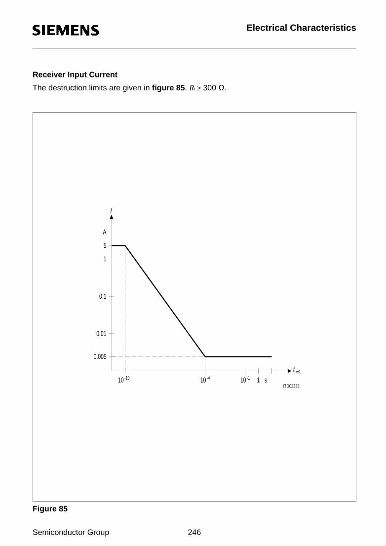
Electrical Characteristics
Receiver Input Current
The destruction limits are given in figure 85. Ri ≥ 300 Ω.
Figure 85
ITD02338
0.005
5
10 -10 -410 -110 1 s
A
w1t
Ι
0.01
0.1
1
Semiconductor Group 246

Electrical Characteristics
DC CharacteristicsTA = 0 to 70 °C; VDD = 5 V ± 5 %, VSSA = 0 V, VSSD = 0 V
Parameter Symbol Limit Values Unit Test Condition Remarks
min max
L-input voltage VIL – 0.4 0.8 V All pinsexceptSX1,2, SR1,2
H-input voltage VIH 2.0 VDD
+ 0.4V
L-output voltageL-output voltage(IDP0)
VOL
VOL1
0.450.45
VV
IOL = 2 mAIOL = 7 mA
H-output voltageH-output voltage
VOH
VOH
2.4VDD
– 0.5
VV
IOH = – 400 µAIOH = – 100 µA
Powersupplycurrent
power
down
ICC 1.5 mA VDD = 5 VInputs atVSS / VDD
No outputloadsexcept SX1,2(50 Ω load)
oper-ational(96 kHz)
15 mA DCL = 512 kHz
17 mA DCL = 1536 kHz
22 mA DCL = 4096 kHz
EmergencyB1 = FFH,B2 = FFH,D = 1
7.7 mA DCL = 1536 kHz
B1 = FFH,B2 = FFH,D = Flag
7.95 mA DCL = 1536 kHz
B1 = 55H,B2 = FFH,D = Flag
8.75 mA DCL = 1536 kHz
B1 = 00H,B2 = FFH,D = Flag
10 mA DCL = 1536 kHz
Input leakagecurrentOutput leakagecurrent
ILI
ILO
10
10
µA
µA
0 V < VIN < VDD to 0 V
0 V < VOUT < VDD to 0 V
All pinsexceptCP/BCL,X2, SX1,2,SR1,2,A0, A1,A3, A4
Semiconductor Group 247

Electrical Characteristics
Note: 1) Due to the transformer, the load resistance seen by the circuit is four times RL.
CapacitancesTA = 25 °C, VDD = 5 V ± 5 %, VSSA = 0 V, VSSD = 0 V, fc =1 MHz, unmeasuredpins grounded.
Input leakagecurrentinternal pull-down
ILIPD 120 µA 0 V < VIN < VDD to 0 V A0, A1,A3, A4,CP/BCL,X2
Absolute valueof output pulseamplitude(VSX2 – VSX1)
VX 2.032.10
2.312.39
VV
RL = 50 Ω1)
RL = 400 Ω1)
SX1,2Transmitter out-put current
IX 7.5 13.4 mA RL = 5.6 Ω1)
Transmitter out-put impedance
RX 100
kΩΩ
Inactive or during binary oneduring binary zero RL = 50 Ω
Receiveroutput voltage
VSR1 2.35 2.6 V IO < 5 µA
SR1,2Receiverthreshold voltageVSR2 – VSR1
VTR 225 375 mV Dependent on peak level
DC CharacteristicsTA = 0 to 70 °C; VDD = 5 V ± 5 %, VSSA = 0 V, VSSD = 0 V (Forts.)
Parameter Symbol Limit Values Unit Test Condition Remarks
min max
Unit
pF
pFpF
pF
Parameter Symbol
Load capacitance CL
Input capacitanceI/O capacitance
CIN
CI/O
Output capacitanceagainst VSSA
COUT
50
77
10
Remarks
min. max.
Limit Values
pFInput capacitance CIN 7
XTAL1,2
All pins exceptSR1,2, XTAL1,2
SX1,2
SR1,2
Semiconductor Group 248

Electrical Characteristics
Recommended Oscillator Circuits
Figure 86Oscillator Circuits Crystal Specification
Note: The load capacitance CL depends on the recommendation of the crystalspecification. Typical values for CL are 22 … 33 pF.
ITS00764
7.68 MHz
XTAL1
2XTAL XTAL 2
1XTAL
N.C.
OscillatorExternal
Signal
Crystal Oscillator Mode Driving from External Source
18
1919
18
pF33
33 pF
C L
LC
Unit
pF
ppm
Parameter Symbol
Load capacitance CL max. 50
Frequency calibration tolerance max. 100
Oscillator mode fundamental
Limit Values
MHzFrequency f 7.680
Semiconductor Group 249
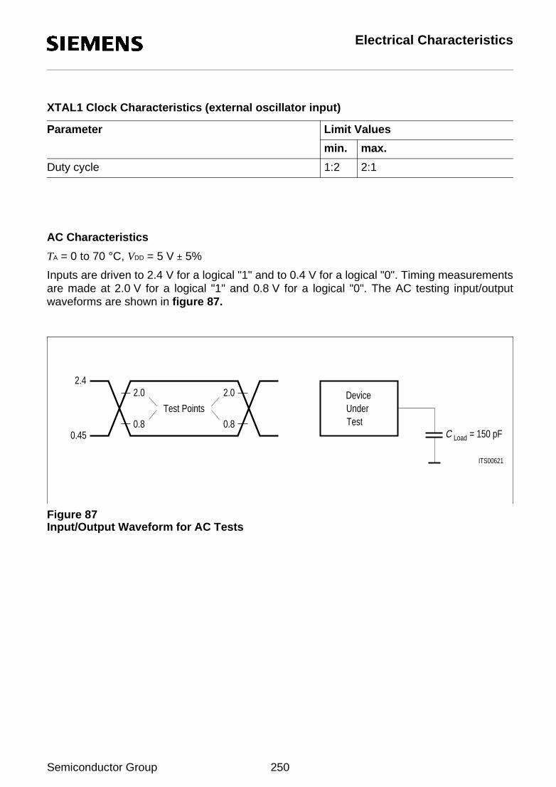
Electrical Characteristics
XTAL1 Clock Characteristics (external oscillator input)
AC Characteristics
TA = 0 to 70 °C, VDD = 5 V ± 5%
Inputs are driven to 2.4 V for a logical "1" and to 0.4 V for a logical "0". Timing measurementsare made at 2.0 V for a logical "1" and 0.8 V for a logical "0". The AC testing input/outputwaveforms are shown in figure 87.
Figure 87Input/Output Waveform for AC Tests
Parameter
Duty cycle 1:2 2:1
min. max.
Limit Values
ITS00621
= 150LoadCTestUnderDevice
0.45
2.42.0
0.80.8
2.0
Test Points
pF
Semiconductor Group 250

Electrical Characteristics
Microprocessor Interface Timing
Siemens/Intel Bus Mode
Figure 88Microprocessor Read Cycle
Figure 89Microprocessor Write Cycle
Figure 90Multiplexed Address Timing
ITT00712
RD x CS
AD0 - AD7
t RD
Data
t DF
RRt t RI
A0 - A7
ITT00713
WR x CS
AD0 -AD7
t DW
Data
t WD
WWt t WI
D0 - D7
ITT00714
WR x CS
AD0 - AD7
t LA
CSxRD
or
Address
ALE
t ALS
t AL
t AA t AD
Semiconductor Group 251

Electrical Characteristics
Figure 91Non-Multiplexed Address Timing
Motorola Bus Mode
Figure 92Microprocessor Read Timing
Figure 93Microprocessor Write Cycle
ITT00715
WR x CS
A0 - A5
t AHt AS
Address
CSxRD
or
ITT00716
CS x DS
D0 - D7
t RD
Data
t DF
DSDt
RRt t RI
R/W
t RWD
Semiconductor Group 252

Electrical Characteristics
Figure 94Non-Multiplexed Address Timing
Microprocessor Interface Timing
ITT00718
CS x DS
AD0
t AHt AS
- AD5
Unit
ns
ns
ns
ns
ns
Parameter Symbol
ALE pulse width tAA 50
Address setup time to ALE tAL 15
Address hold time from ALE tLA 10
Address setup time tAS 25
Address hold time tAH 10
min. max.
Limit Values
nsAddress latch setup time to WR, RD tALS 0
nsALE guard time tAD 15
nsDS delay after RW setup tDSD 0
nsRD pulse width tRR 110
nsData output delay from RD tRD 110
nsData float from RD tDF 25
nsRD control interval tRI 70
nsW pulse width tWW 60
nsData setup time to W × CS tDW 35
nsData hold time from W × CS tWD 10
nsW control interval tWI 70
Semiconductor Group 253
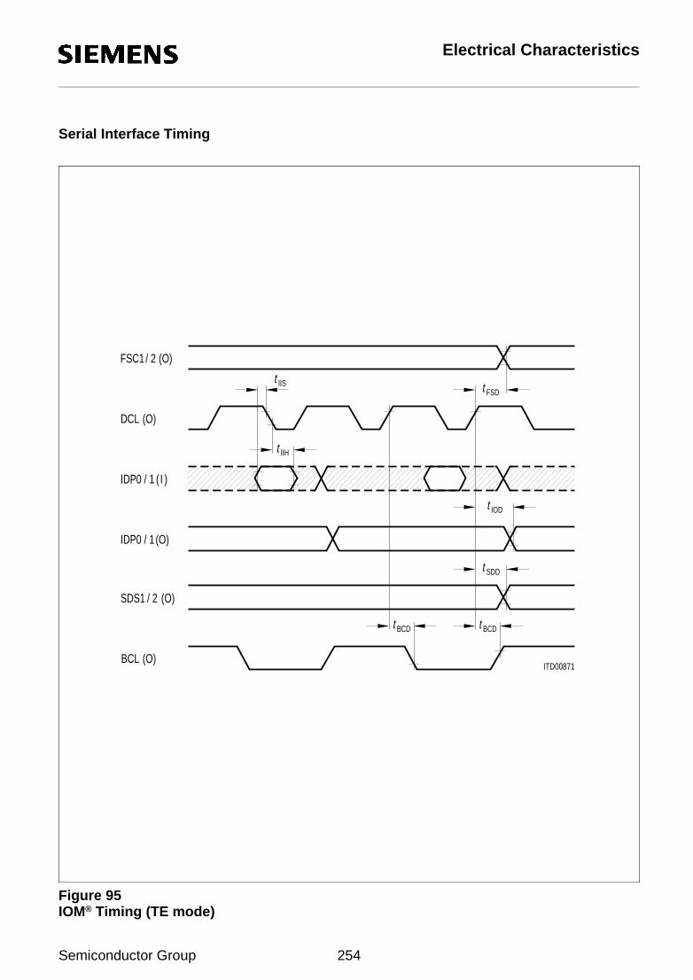
Electrical Characteristics
Serial Interface Timing
Figure 95IOM® Timing (TE mode)
ITD00871
t FSD
t IIS
IIHt
t IOD
BCDtBCDt
SDDt
(O)FSC1
DCL (O)
( )IDP0 / 1
(O)SDS1
(O)BCL
Ι
/ 2
/ 2
IDP0 / 1 (O)
Semiconductor Group 254

Electrical Characteristics
Figure 96IOM® Timing (LT-S, LT-T, NT mode) IOM® Timing
t FSS
t FSH
t FSW
FSC
DCL ( I )
( I )1/2
t FDD
FSD (O)
0/1 ( I )IDP
IIHt
IISt
(O)0/1IDP
Bit 0
Bit 0
SDDt
SDS1/2 (O)
t IOD
ITD00872
Unit
nsns
nsns
ns
ns
ns
Parameter Symbol
IOM output data delay tIOD 2020
IOM input data setup tIIS 4 + tWH
20
IOM input data hold tIIH 20
Strobe signal delay tSDD
Bit clock delay tBCD – 20
140100
120
20
min. max.
Limit Values
nsFSC1/2 strobe delay tFSD – 20 20
nsFrame sync setup tFSS 50
nsFrame sync hold tFSH 30
nsFrame sync width tFSW 40
nsFSD delay tFDD 20 140
Test Condition
IOM-1IOM-2
IOM-1IOM-2
Semiconductor Group 255
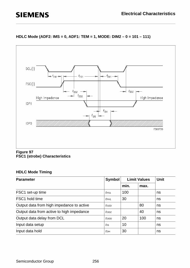
Electrical Characteristics
HDLC Mode (ADF2: IMS = 0, ADF1: TEM = 1, MODE: DIM2 – 0 = 101 – 111)
Figure 97FSC1 (strobe) Characteristics
HDLC Mode Timing
Unit
ns
ns
ns
ns
ns
Parameter Symbol
FSC1 set-up time tFS1 100
FSC1 hold time tFH1 30
Output data from high impedance to active tOZD
Output data delay from DCL tODD 20
Input data setup tIS 10
80
100
min. max.
Limit Values
nsOutput data from active to high impedance tODZ 40
nsInput data hold tDH 30
Semiconductor Group 256

Electrical Characteristics
Serial Port A (SSI) Timing
Figure 98SSI Timing (TE, timing mode 0)
Serial Port A (SSI) Timing
ITD00873
t SCD
t SSH
t SCD
t SSS
t SSD
t FSD
B2( B1 ) Channel* B1( B2 ) Channel*
SCA
SDAR
SDAX
O* Default polarityIndividual B-channel switching to the B1-selected by programming the output polarity of FSC1 and FSC2in the ADF1 register
DCL (0)
:= Output
or B2 channel can be
(0)1/2FSC
Unit
ns
ns
ns
ns
Parameter Symbol
SCA clock delay tSCD 20
SSI data delay tSSD 20
SSI data setup tSSS 40
FSC1/2 strobe delay tFSD – 20
140
140
20
min. max.
Limit Values
nsSSI data hold tSSH 20
Semiconductor Group 257

Electrical Characteristics
SLD Timing
Figure 99SLD Timing (TE mode)
Figure 100SLD Timing (LT-S / LT-T mode) SLD Timing
ITD00874
SLDSLD
t SLS
SLHtSLDt
t FSD
DCL (0)
(I/O)SIP
IN OUT
(0)1/2FSC
ITD00875
t FSS
t FSH
t FSW
t SLD t SLH t SLS
FSC
DCL
SIP (I/O)
(I)
(I)1
Unit
ns
ns
ns
ns
ns
Parameter Symbol
SLD data delay tSLD 20
SLD data setup tSLS 30
SLD data hold tSLH 30
Frame sync setup tFSS 50
Frame sync hold tFSH 30
140
min. max.
Limit Values
nsFSC1/2 strobe delay tFSD – 20 20
nsFrame sync width tFSW 40
Semiconductor Group 258

Electrical Characteristics
Clock Timing
The clocks in the different operating modes are summarized in tables 25 – 27,with the respective duty ratios.
Table 25ISAC®-S Clock Signals (IOM®-1 mode)
Table 26ISAC®-S Clock Signals (IOM®-2 mode)
DCLKApplication M1 M0
o:512 kHz*1:2
i:512 kHz
i:512 kHz
i:512 kHz
TE
LT-T
LT-S
NT
0
0
1
1
0
1
0
1
FSC1/2
o:8 kHz*1:1
i:8 kHz
i:8 kHz
i:8 kHz
CP
o:1536 kHz*3:2
o:512 kHz*1:2
–
–
X1
o:3840 kHz1:1
–
o:7680 kHz1:1
–
DCLApplication M1 M0
o:1536 kHz*3:2
i:4096 kHz
i:4096 kHz
i:512 kHz
TE
LT-T
LT-S
NT
0
0
1
1
0
1
0
1
FSC1 FSC2
o:8 kHz*1:2
i:8 kHz i:8 kHz
i:8 kHz i:8 kHz
i:8 kHz i:8 kHz
X1
–
–
o:7680 kHz1:1
–
SDS1/2
o:8 kHz1:112:10
o:8 kHz1:112:10
o:8 kHz1:112:10
o:8 kHz1:112:10
CP/BCL
o:768 kHz*1:1
o:512 kHz*1:2
–
–
*) Synchronous to receive "S" line
Semiconductor Group 259

Electrical Characteristics
The 1536-kHz clock (TE mode) and the 512-kHz clock (LT-T mode) are phase-locked to thereceive S signal, and derived using the internal DPLL and the 7.68 MHz ± 100 ppm crystal.
A phase tracking with respect to "S" is performed once in 250 µs. As a consequence of thisDPLL tracking, the "high" state of the 1536-kHz clock may be either reduced or extended byone 7.68-MHz period (duty ratio 2:2 or 4:2 instead of 3:2) once every 250 µs. Since the othersignals are derived from this clock (TE mode), the "high" or "low" states may likewise bereduced or extended by the same amount once every 250 µs.
The phase relationships of the clocks are shown in figure 101.
Figure 101Phase Relationships of ISAC®-S Clock Signals
The timing relationships between the clocks are specified in figure 98 and table 28.
ITD00876
7.68 MHz
kHz1536
768 kHz
*
Synchronous to receive S/T. Duty Ratio 3:2 Normally*
3840 kHzX1:
kHz512
Semiconductor Group 260

Electrical Characteristics
Figure 102Timing Relationships between ISAC®-S Clock Signals
ITD02393
CP
DCL
BCL
FSC1/2
SDS1/2
t BCDt BCD
FCPt
t FSD
SBDtt SSD
DCDtDCDt
DCL
R(IOM -1)
-2)(IOM R
(IOM -1)R
Semiconductor Group 261

Electrical Characteristics
Table 27
Tables 29 to 33 give the timing characteristics of the clocks.
Figure 103Definition of Clock Period and Width
Table 28DCL Clock Characteristics (IOM®-1)
Unit
ns
ns
ns
ns
ns
Parameter Symbol
Bit clock delay tBCD – 20
SDS1/2 delay from DCL tSDD
SDS1/2 delay from BCL tSBD
FSC1/2 delay from CP tFCP 0
FSC1/2 delay from DCL tFSD – 20
20
120
120
50
20
min. max.
Limit Values
nsDCL delay from CP tDCD 0 50
Conditions
IOM-2
IOM-2
IOM-2
IOM-1
IOM-1
IOM-1
ITT00723
t WH WLtt P
3.5 V
V0.8
Unit
ns
ns
ns
ns
ns
Parameter Symbol
(TE) 512 kHz tPO 1822
(TE) 512 kHz 1:2 tWHO 470
(TE) 512 kHz 1:2 tWLO 1121
(NT, LT-S, LT-T) tWHI 200
(NT, LT-S, LT-T) tWLI 200
2084
832
1483
min. max.
Limit Values
ns(NT, LT-S, LT-T) tPI 1853 2053
Test Condition
osc ± 100 ppm
osc ± 100 ppm
osc ± 100 ppm
1953
651
1302
typ.
Semiconductor Group 262

Electrical Characteristics
Table 29DCL Clock Characteristics (IOM®-2)
Note: For NT characteristics, see IOM-1 case.
Table 30CP Clock Characteristics (IOM®-1 TE mode)
Table 31CP Clock Characteristics (LT-T mode)
Table 32X1 Clock Characteristics (TE mode)
Unit
ns
ns
ns
ns
ns
Parameter Symbol
(TE) 1536 kHz tPO 520
tWHO 240
tWLO 240
tWHI 100
tWLI 100
782
541
281
min. max.
Limit Values
ns(LT-S, LT-T) 4096 kHz tPI 240
Test Condition
osc ± 100 ppm
osc ± 100 ppm
osc ± 100 ppm
651
391
260
typ.
244
Unit
ns
ns
ns
Parameter Symbol
(TE) 1536 kHz tPO 520
tWHO 240
tWLO 240
782
541
281
min. max.
Limit Values Test Condition
osc ± 100 ppm
osc ± 100 ppm
osc ± 100 ppm
651
391
260
typ.
Unit
ns
ns
ns
Parameter Symbol
(LT-T) 512 kHz tPO 1822
tWHO 470
tWLO 1121
2084
832
1483
min. max.
Limit Values Test Condition
osc ± 100 ppm
osc ± 100 ppm
osc ± 100 ppm
1953
651
1302
typ.
Unit
ns
ns
ns
Parameter Symbol
(TE) 3840 kHz tPO – 100 ppm
tWHO 120
tWLO 120
100 ppm
140
140
min. max.
Limit Values Test Condition
osc ± 100 ppm
osc ± 100 ppm
osc ± 100 ppm
260
130
130
typ.
Semiconductor Group 263

Electrical Characteristics
Table 33X1 Clock Characteristics (LT-S mode)
Jitter
In TE mode, the timing extraction jitter of the ISAC-S conforms to CCITT RecommendationI.430 (– 7% to + 7% of the S-interface bit period).
In the NT and LT-S applications, the clock input DCL is used as reference clock to provide the192-kHz clock for the S-line interface. In the case of a plesiochronous 7.68-MHz clockgenerated by an oscillator, the clock DCL should have a jitter less than 100 ns peak-to-peak.(In the case of a zero input jitter on DCL the ISAC-S generates at most 130 ns "self-jitter" onthe S interface.)
In the case of a synchronous*) 7.68-MHz clock (input XTAL1), the ISAC-S transfers the inputjitter of XTAL1, DCL and FSC1 to the S interface. The maximum jitter of the NT/LT-S output islimited to 260 ns peak-to-peak (CCITT I.430).
Description of the Transmit PLL (XPLL) of the ISAC®-S
Function of the XPLL
The XPLL generates a 1.536-MHz clock synchronized to the DCL 512-kHz clock bymodification of the counter’s divider ratio. The 1.536-MHz clock is then divided to 192 kHz and512 kHz. The 512 kHz is used as the looped back clock and compared to the 512-kHz DCL inthe phase detector. A four bit up/down counter integrates the phase information to preventtracking steps in presence of high frequency input jitter (see figure 99).
Jitter considerations in case of a synchronous 7.68-MHz clock
After the XPLL has locked once, no more tracking steps are performed because there is a fixeddivider ratio of 15 between 7.68 MHz and DCL. Therefore the input jitter at DCL and 7.68 MHzis transferred transparently to the S/T interface (192 kHz).
Jitter considerations in case of a plesiochronous 7.68-MHz clock (crystal)
Each tracking step of the XPLL produces an output jitter of 130 ns pp. In case of non-zero inputjitter at DCL, this input jitter is increased by 130 ns pp. However, if the input jitter frequency ishigh enough (in the range of 25 kHz and higher) the four bit up/dn counter works as a loop filterand thus the XPLL attenuates the input jitter to zero.
Unit
ns
ns
ns
Parameter Symbol
(LT-S) 7680 kHz tPO – 100 ppm
tWHO
tWLO
100 ppm
min. max.
Limit Values Test Condition
osc ± 100 ppm
osc ± 100 ppm
osc ± 100 ppm
130.21
65
65
typ.
*) fixed divider ratio between XTAL1 and DCL
Semiconductor Group 264

Electrical Characteristics
That means that the output jitter will not exceed 130 ns pp. In the intermediate range of jitterfrequency, the degree of jitter attenuation lies between zero and the maximum (seefigure 105).
Figure 104Block Diagram of XPLL
Figure 105Jitter Transfer Curve of XPLL
ITS02394
Divider:
Divider
DividerPhaseDetector
Up/DownCounter
LagLead
Up
Down
DCL
5 ± 1 8
3
DCL 8
512 kHz
1.536 MHz
7.68 MHz
192 kHz
512 kHzDCL
:
:
:
R(IOM -1 Mode)(IOM -2 Mode)R
ITD02395
0
20
40
Attenuation
SinusoidalJitter Frequency
dB
1 Hz Hz10 Hz100 kHz1 10 kHz25 kHz
100 kHz 1 MHz
Semiconductor Group 265

PEB 2086
Description of the receive PLL (RPLL) of the ISAC-S
The receive PLL performs phase tracking each 250 µs after detecting the phase between theF/L transition of the receive signal and the recovered clock. Phase adjustment is done byadding or subtracting 130 ns to or form a 1.536-MHz clock cycle. The 1.536-MHz clock is thanused to generate any other clock synchronized to the line.
During (re)synchronization an internal reset condition may effect the 1.536-MHz and 512-kHzclocks to have high or low times as short as 130 ns. After the S/T interface frame has achievedthe synchronized state (after three consecutive valid pairs of code violations) the FSC outputin TE mode is set to a specific phase relationship, thus causing once an irregular FSC timing.
Reset
Table 34Reset Signal Characteristics
Figure 106
Unit
ms
Parameter Symbol
Length of activehigh state
tRST 4
2 × DCLclock cycles
min.
Limit Values Test Condition
Power on/Power Downto Power Up (Standby)
During Power Up (Standby)
ITD02396
RST
t RST
Semiconductor Group 266

PEB 2086
Timing Characteristics of PEB 2086 Specific Functions
External Trigger for the S-Frame Synchronization (LT-S, NT-mode)
Figure 107External Trigger for the S-Frame Synchronization
Parameter Symbol Limit Values Unit
min. max.
Frame sync setup tFSS 50 ns
Frame sync hold tFSH 30 ns
Frame sync width tFSW 40 ns
M-bit input setup tMIS 50 ns
M-bit input hold tMIH 30 ns
DCL(i)
FSC1(i)
X2(i)
Timing (LT-S Mode)
t FSH
ITT03237
CP(i)
FSWt
t FSS
MIHtt MIS
RIOM
Semiconductor Group 267

PEB 2086
Multiframe Synchronization Output (TE-mode)
Figure 108Multiframe Synchronization Output
Parameter Symbol Limit Values Unit
min. max.
FSC 1/2 strobe delay tFSD – 20 20 ns
M-bit width tWD 80 µs
M-bit delay to DCL tMD 150 ns
DCL(O)
FSC1(O)
X2(O)
Timing (TE-Mode)
t FSD
MDtITT03238
t WD
RIOM
Semiconductor Group 268

PEB 2086
Frame Relationship and Multiframe Synchronization in LT-S, NT-Mode
Please see chapter 2.3.1 for differences between Timing Mode 0 and Timing Mode 1.
Timing Mode 0
The timing relationship between the IOM-interface and the S/T-interface in IOM-1 timingmode 0 is shown in figure 109.
Figure 109Frame Relationship in Timing Mode 0
1) Internal delays are dependent on temperature, VDD and fabrication parameters.
Parameter Symbol Limit Values
S-interface to FSC-delay tSFD 16 µs ± 300 ns1) ± 130 ns (jitter)
10
0
D L. L. B1 E D AF NA B2 MDE B1 B2E D S L.FDE
NT to TE
FSC2(i)
X2(i)
IDP1(i)
ITD03736
CP(i)
t SFD
B1 B2 B1 B2
F L.
Semiconductor Group 269

PEB 2086
Timing Mode 1
In timing mode 1, CP(i) and X2(i) occur 1/8 × 125 µs earlier together with FSC 1.
Figure 110Frame Relationship in Timing Mode 1
1) Internal delays are dependent on temperature, VDD and fabrication parameters.
Parameter Symbol Limit Values
S-interface to FSC-delay tSFD 16 µs ± 300 ns1) ± 130 ns (jitter)
10
0
D L.F L. B1 E D A F NA MDE B2E D S L.FDE
NT to TE
FSC2(i)
X2(i)
IDP1(i)
ITD03737
FSC1(i)
t SFD
B1 B2 B1 B2
t SFD
CP(i)
B2 E
FramePeriod
1 / 8
PeriodFrame
1 / 8
B2 B1 L.
Semiconductor Group 270

Electrical Characteristics
Frame Relationship in TE-Mode
The relationship between the S/T-interface and the IOM-interface in TE IOM-1 mode is shownin figure 111. The pin X2 provides the M-bit during bits 0 through 23 and 26 through 31 of anIOM-frame. It is recommended to sample the state of the M-bit with the falling edge of FSC 1.At bit positions 24 and 25, the D-ECHO-bits appear according to the PEB 2085 functionality.
Figure 111Frame Relationship in TE-Mode
1) Internal delays are dependent on temperature, VDD and fabrication parameters. The values may be reducedafter evaluation.
Parameter Symbol Limit Values
S-interface to IOM-delay tSID 121 µs ± 300 ns1) ± 260 ns (jitter)
IOM-interface to S-delay tISD 4 µs ± 300 ns1) ± 260 ns (jitter)
10
0
D F L. B1 E D A F NA B2 MDE E D S E
B1 B2
t SID
NT to TE
FSC(O)
X2(O)
IDP0(O)ITD03738
B2B1
Mi+2
Mi+1 Mi+1 i+2Mi+1MMi
t ISD
E E
L. B1 B2 L. F L.D
Semiconductor Group 271

Low Level Controller
6 ISAC®-S Low Level Controller
The following paragraphs outline the functionality and structure of a software driver examplefor the ISAC-S. This example is based on the Siemens Low Level Controllers (LLC’s) for BasicAccess IC which are available in C source code. The ISAC-S software driver will be alsoreferred to as LLC or ISAC-S LLC.
It should be noted that the ISAC-S LLC does not access the complete palette of device funtionsbut rather a subset of them. For example not all message transfer modes are supported.Please refer to paragraph ’Architecture and Functions’ for a more detailed description.
The ISAC-S LLC presented here has been successfully tested in the Siemens ISDN PCdevelopment system. Correct operation with a higher layer software has been verified by usingthe Siemens ISDN Software Development and Evaluation System (SIDES) and the SiemensISDN Operational Software (IOS).
6.1 Architecture and Functions
The ISAC-S LLC may be divided into two major parts, one for Layer 1 control, the ’SBC part’and one for directing the HDLC controller operations, the ’ICC part’. The naming conventions’SBC part’ and ’ICC part’ have been introduced because the Low Level Controllers (LLC’s) forBasic Access ICs use the same code to control either an ISAC-S or and ICC - SBC(X)combination.
The ISAC-S LLC consists of driver functions and interrupt server. The driver functions areimplemented as a set of C functions which are responsible for interpreting hardware relatedcommands from the higher layers and carrying out the appropriate actions at the hardwarelevel. Driven by hardware interrupts, the interrupt server analyses the hardware event andinforms the higher software layers of that event.
It should be noted that this implementation has attempted to remove as many protocol specificfunctions as possible from the LLC and to locate them instead in the higher layer protocol itself.This has the advantage of making the LLC- more general and less likely to be in need of re-programming for different protocols.
Semiconductor Group 272

Low Level Controller
OPERATING SYSTEM andHigher Level Protocol Software
Figure 112LLC Architecture
The ISAC-S LLC supports following standard functions:
– Initialization of the SBC (layer 1) part.– Activation of layer 1.– Deactivation of layer 1.
HDLC controller initialization.The following HDLC controller message transfer modes are supported:
automode: full two byte address compare, LAPD support.non-automode: full two byte address compare.transparent mode 3: high byte address compare; called 'TRANSPARENT' mode in
the LLC.transparent mode 2: no address compare; called 'EXTENDED TRANSPARENT'
mode in the LLC.
HDLC framing with two byte address field is assumed.
ITS02392
HDLC Controllerrelated Functions
Driver Functions
ICC Part ICC PartSBC Part SBC Part
Layer-1Functions
FUNCTION CALLS
. . .Status/
Error MessagesReceivedFrames
MMU ServiceRequests
Interrupt Server
Evaluation of Interrupt Cause
RISAC -S TE
Semiconductor Group 273

Low Level Controller
– HDLC frame transmission.– Programming of TEI and SAPI values.– HDLC transceiver control.– Interrupt handling.– Local test loop switching.– B-Channel switching in IOM-1 configurations.
TE configurations in IOM-1 / IOM-2 mode and NT-S configurations (IOM-1 only) are supported.
In addition to the ISAC-S standard functions supporting the ISDN basic access, the ISAC-Scontains optional, terminal specific functions. These terminal specific functions (watchdog andexternal awake) are not supported by this LLC.
6.2 Summary of LLC Functions
6.2.1 Layer 1 Related Functions
Mnemonic PurposeActL1_SBC Layer-1 activation.DeaL1_SBD Layer 1 deactivation.ArlL1_SBC Activation of a local loop.EnaClk_SBC Enable clocking in power down mode.InitL1_SBC Layer-1 initialization and reset.ResL1_SBC Layer-1 reset.
IntL1_SBC Handling of CISQ interrupts.
The layer 1 related functions call DECODE_L1_STATUS to report a L1 status change to ahigher layer software.
6.2.2 HDLC Controller Related Functions
Mnemonic PurposeInitLay2_ICC HDLC controller initialization.Loop_ICC Testloop activation at the serial outputs of the IOM interface.ResetHDLC_ICC HDLC transceiver reset.RecReady_ICC Setting the HDLC receiver ready or not ready.SendFrame_ICC HDLC frame transmission.StoreSAPI_ICC SAPI programming.StoreTEI_ICC TEI programming.SwitchB_ICC B-channel switching to SSI or SLD interface in IOM1 configurations.
Int_ICC Handling of XPR, RSC, TIN and EXI interrupts.Rx_ICC Handling of RPF and RME interrupts.
Semiconductor Group 274
Low Level Controller
6.2.3 External Functions
The LLC program listing shows some references to external functions (indicated by an ’IMPORT’ declaration). These functions are used by the LLC but are not part of it. These external functions must be provided by the operating system or a higher layer protocol software.
MMU_req ()
By calling MMU_req the ISAC-S LLC requests memory for the temporary storage of a received data frame. The memory management unit (MMU) of the operating system has to provide a memory buffer of the required size (max. 260 bytes).
MMU_free ()
MMU_free is the counterpart to MMU_req. The operating system can release a previously allocated memory buffer.
STRING_IN () and STRING_OUT ()
STRING_IN and STRING_OUT are assembler written functions for fast input and output of data frames from/to the ISAC-S FIFO.
ENTERNOINT () and LEAVENOINT ()
ENTERNOINT and LEAVENOINT are called to disable and enable all system interrupts in time critical sections.
Decode_S_Frame_BASIC ()
Decode_S_Frame_BASIC is called by the LLC interrupt server to transfer a received HDLCS frame to a higher layer protocol software.
Following information is passed to Decode_S_Frame_BASIC:
’pei’: 1 byte value identifying the performed address recognition. The bits 0, 1 and 2 of’pei’ represent the bits TA, SA0 and SA1 of the ISAC-S’ RSTA register.
’sapi’: 1 byte value representing the received HDLC SAPI address byte. Bit 1 of ’sapi’ isthe C/R bit value (RSTA:CR). The most significant 6 bits of ’sapi’ are 0 inauto-mode, non-auto-mode and transparent mode.
’tei’: 1 byte value representing the received HDLC TEI address byte. ’tei’ is 0 inauto-mode and non-auto-mode.
’ctrl’: 2 byte value representing the contents of the received HDLC control field.
’frame_status’: 1 byte value= 0 × 00: frame is valid.= 0 × 80: frame is mutilated (last byte of two byte control field missing).= 0 × 82: frame is too long. S-frame with I-field.
’M128’: 1 byte value. 0 in modulo 8 operating mode (1 byte control field), 1 in modulo 128 operating mode (2 byte control field). For correct decoding of ’ctrl’ above.
Semiconductor Group 275

Low Level Controller
Decode_U_Frame_BASIC ()
Decode_U_Frame_BASIC is called by the LLC interrupt server to transfer a received HDLC Uframe to a higher layer protocol software.
Following information is passed to Decode_U_Frame_BASIC:
’pei’: (refer to Decode_S_Frame).
’sapi’: (refer to Decode_S_Frame).
’tei’: (refer to Decode_S_Frame).
’ctrl’: 1 byte value representing the contents of the received HDLC control field.
PassLongFrame_BASIC ()
PassLongFrame_BASIC is called by the LLC interrupt server to transfer received HDLC I andUI frames to a higher layer protocol software.
The LLC passes a pointer to a structure (FRAME_PASS) containing information about thereceived frame to PassLongFrame_BASIC. Please refer to the following paragraph for adescription of this structure.
Semiconductor Group 276

Low Level Controller
6.3 LLC Code Elements
6.3.1 Structures
The Structure ’PEITAB’
As the various routines in the LLC require facilities to store information about the device theycontrol, information structures have been introduced. One of these structures is namedPEITAB. A variable of type PEITAB contains all relevant information about the HDLC controllerand L1 part. The LLC uses the external function GetPEITAB_BASIC to get a pointer to thecorresponding PEITAB variable. The following section deals with the important elements ofPEITAB.
Status Information
pt_op_mode operating mode of the ISAC-S HDLC controller (auto-mode, non-auto-mode…)
pt_state Flags of 'pt_state' indicate the various device states.pt_ModulMode hardware configuration (TE or NT-S)
I/O buffer related elements
These elements are used when the HDLC data is transmitted or received. In both the transmitand receive directions additional RAM is required to store data on an intermediate basis. Thisbuffer will be referred to as the data frame. Related information is stored in the followingelements:
Transmit buffer pointers
pt_tx_start pointer to the starting point of the data frame for transmissionpt_tx_curr pointer to the present byte to be sent
Receive buffer pointers
pt_rx_start pointer to the starting point of the receive data frame.pt_rx_curr pointer to the next free position in the receive buffer.
Data byte counters
pt_tx_cnt number of bytes yet to be transmittedpt_rx_cnt number of bytes currently received
The following elements are used to store the type of frame:
pt_rx_frame type of received frame.pt_tx_frame type of transmitted frame.
Register addresses are contained in those structure elements which have the prefix pt_rfollowed by the register mnemonic. For example pt_r_fifo contains the address of the ISAC-SXFIFO/RFIFO, pt_r_mode the address of the ISAC-S MODE register, etc.
Semiconductor Group 277

Low Level Controller
The Structure ’FRAME_PASS’
The variable ’fp’ of the type FRAME_PASS is used when the LLC interrupt server has receiveda valid HDLC I or UI frame. A pointer to ’fp’ is passed to PassLongFrame_BASIC.FRAME_PASS contains all information about the received HDLC frame. Following elementsare used:
mmu_buff start of MMU buffer which is used for the temporary storage of that HDLCframe.
start_of_i_data Start of the I data field in this MMU buffer.
i_data_cnt Number of bytes in the I data field.
Two_byte_cf 0 for a one byte HDLC control field, 1 for a two byte HDLC control field.
ctrl_field HDLC control field.
pei 1 byte value identifying the performed address recognition. The bits 0, 1and 2 of ’pei’ represent the bits TA, SA0 and SA1 of the ISAC-S’ RSTAregister.
frame Type of HDLC frame; 0 = I-frame, 1 = UI-frame.
sapi Received HDLC SAPI address byte. Bit 1 of ’sapi’ is the C/R bit value(RSTA:CR). The most significant 6 bits of ’sapi’ are 0 in auto-mode, non-auto-mode and transparent mode.
tei Received HDLC TEI address byte. ’tei’ is 0 in auto-mode and non-automode.
6.3.2 Definitions and Naming Conventions
All expressions in capital letters are definitions contained in the include files def.h, conf.h andbasic.h. These include files are not part of the following C source listing. ISAC-S LLC specificdefinitions are explained in the following paragraphs.
Public functions are declared with an EXPORT (only for better readability). External functionsare imported using an IMPORT which is the redefinition of C’s ’extern’. Any function which isonly used locally is declared with a LOCAL (= ’static’).
6.3.2.1 Type Definitions
For reference here is a list of the type definitions used in the LLC’s.
type definitions meaning
BYTE one byte value
WORD word = two byte value
FPTR far pointer to BYTE
Semiconductor Group 278

Low Level Controller
6.3.2.2 Macro Definitions
Error conditions and other states of the ISAC-S must be reported to higher layers. Thisreporting is realized by a few macros which are executed when such conditions are detected.These macros can be mapped to any form of message a higher layer software requires. Anykind of immediately necessary actions may be defined in those macros as well. By using suchconstructs the code can be kept compact and clearly readable.
Layer 1 Related Status Message
DECODE_L1_STATUS for L1 status (IC channel indication) decoding.
HDLC Controller Related Status and Error Messages
CRC_ERROR CRC error.
MISSING_ACKNOWLEDGE A ’Missing HDLC I-frame acknowledge’ is generatedwhen an acknowledge message for a previouslysent I-frame is outstanding and the HDLC messagetransfer mode is changed from auto-mode to non-auto-mode. An outstanding acknowledge isindicated by the ISAC-S in register STAR2 (’timerrecovery status’ and ’waiting for acknowledge’ bits).
MMU_ERROR No memory available to store incoming frame.
N201_ERROR N201 error, HDLC frame is too long.
PEER_REC_READY Peer receiver ready.
PEER_REC_BUSY Peer receive busy.
PROTOCOL_ERROR Protocol error (PCE interrupt).
REC_FRAME_OVERFLOW Receive frame overflow.
REC_DATA_OVERFLOW Receive data overflow (RDO interrupt).
REC_ABORTED Receive aborted (RAB interrupt).
TX_ACKNOWLEDGE Transmit frame acknowledge.
TIN_ERROR TIN interrupt, status enquiry.
TX_DATA_UNDERRUN Transmit data underrun (XDU interrupt).
XMR_ERROR Transmit message repeat indication (XMR interrupt).
Following macros are used when a ’timer recovery status’ (register STAR2, bit TREC) isrecognized.
ENABLE_TREC_STATUS_CHECK enable ’timer recovery status’ check procedure.
DISABLE_TREC_STATUS_CHECK disable ’timer recovery status’ check procedure.
Semiconductor Group 279
Low Level Controller
6.3.2.3 Register Bit Definitions
To facilitate reading and debugging of the code, the bits of many registers are defined asfollows:
The definitions
#define ISTA_RME (BYTE)0x80#define ISTA_RPF (BYTE)0x40#define ISTA_RSC (BYTE)0x20#define ISTA_XPR (BYTE)0x10#define ISTA_TIN (BYTE)0x08#define ISTA_CIC (BYTE)0x04#define ISTA_SIN (BYTE)0x02#define ISTA_EXI (BYTE)0x01
specify the bits of the ISAC-S interrupt status register (ISTA).
6.4 Interrupts
Int_ICC is to be called in the case of ISAC-S interrupts. The following interrupts are handleddirectly in Int_ICC:
’Transmit pool ready’ interrupt (ISTA:XPR)
’Timer’ interrupt (ISTA:TIN).
’Receive Status Change’ interrupt (ISTA:RSC).
’Extended’ interrupt (ISTA:EXI).
The ’Receive Pool Full’ (ISTA:RPF) and ’Receive Message End’ (ISTA:RME) interrupts arehandled by function RX_ICC. The ’CI or SQ channel change’ interrupt (ISTA:CISQ) is handledby IntL1_SBC.
Please note that the following interrupts are not handled by the interrupt service routinedescribed here:
ISTA:SIN (synchronous transfer interrupt)EXIR:SOV (synchronous transfer overflow)EXIR:MOS (monitor status) is handled by external functions which are not part of this
description.EXIR:SAW (subscriber awake)EXIR:WOV (watchdog timer overflow)
Semiconductor Group 280

Low Level Controller
6.5 LLC Routine Reference
6.5.1 ISAC®-S Layer-1 Functions: The SBC Part
ActL1_SBC ()
Initiates layer-1 activation. The appropriate CI code (activate request) is written to the CIchannel if the layer 1 is not already activated. ActL1_SBC then returns with ACK_DONE. Thesubsequent status changes of the SBC will cause CI channel status change (CISQ) interruptsand these will be evaluated in the layer-1 interrupt service routine IntL1_SBC.
If the layer 1 is already activated nothing is carried out but ActL1_SBC calls DECODE_L1_STATUS to report the activated state.
DeaL1_SBC ()
Initiates layer 1 deactivation. The appropriate CI code is written to the CI channel if the layer 1is not already deactivated. The subsequent layer 1 status changes cause CI channel statuschange (CISQ) interrupts and these will be evaluated in the layer 1 interrupt service routineIntL1_SBC.
If the layer 1 is already deactivated nothing is carried out but DeaL1_SBC callsDECODE_L1_STATUS to report the deactivated state.
ArL1_SBC ()
Activates a local loop in the SBC. The appropriate CI code (activate request loop) is written tothe SBC. ArL1_SBC returns with ACK_DONE. The subsequent status changes of the SBC willgenerate CISQ interrupts and these will be evaluated and reported in the layer-1 interruptservice routine IntL1_SBC.
EnaClk_SBC ()
EnaClk_SBC enables clocking in TE configurations when the layer 1 is in power down state.If first tests if clocks are actually there. If there are clocks the function returns with FALSE. Ifthere are no clocks (power down state) the power-up procedure is implemented. The SPU bitin register SPCR is set. The TIM code is written to the CI channel. EnaClk_SBC waits until thepower up state (PU) is indicated before the SPU bit is reset to 0. The routine then returns withTRUE.
InitL1_SBC ()
Initializes and resets the layer-1 controller (ResL1_SBC). Timing mode 0 is set and the TICbus address is also programmed.
Semiconductor Group 281

Low Level Controller
ResL1_SBC ()
This routine resets the layer 1 part of an ISAC-S. It also checks that the layer 1 part is operatingcorrectly.
Reset procedure:
A software reset command (RS) is sent to the layer 1 part via the IOM CI0 channel.ResL1_SBC waits for the expected new state (EI) if no timeout condition occurs and issues arelease command (DIU).
If the new state (EI) is not observed the ISAC-S layer 1 part will be deemed to be defective.
IntL1_SBC () Interrupt Handler
Handles the CISQ interrupts which indicate changes in the layer 1 status. The finalconfirmation of deactivation is carried out here. The actual layer 1 state is evaluated by readingregister CIR0. The following is then carried out:
If the CI channel indication is ’pending deactivation’ state (DR), DIU is sent to deactivate thelayer 1.
If the indication is an ’activation indication’ (AI) the activation must be confirmed from the TEside. IntL1_SBC does it automatically by writing an ’activation request’ (AR). In this way thisrequirement of the ISAC-S is transparent to the higher protocol layers.
After every CI channel status change interrupt (CISQ) DECODE_L1_STATUS is called toreport the current layer-1 state.
6.5.2 ISAC®-S HDLC Controller Related Functions: The ICC Part
InitPeitab_ICC ()
Initializes the local variable ’pt’. InitPeitab_ICC is to be called once during the systeminitialization phase.
InitLay2_ICC ()
Initializes the HDLC controller. The function arguments allow the selection of the HDLCcontroller message transfer mode (auto-mode, non-auto-mode, ...), one or two byte HDCLcontrol field operation (modulo 8 or 128) and the setting of the ISAC-S internal hardware timer.
After InitLay2_ICC is called the TEI values for a Broadcast Link are programmed (TEI = FFhex). The HDLC controller is not reset.
StoreTEI_ICC ()
StoreTEI_ICC is used to program a TEI value in register TEI1 or TEI2 depending on thefunction argument value.
Semiconductor Group 282

Low Level Controller
StoreSAPI_ICC ()
StoreSAPI_ICC is used to program a SAPI value in register SAP1 or SAP2 depending on thefunction argument value.
RecReady_ICC ()
Sets HDLC receiver ready or not ready depending on the function argument value.
ResetHDLC_ICC ()
ResetHDLC_ICC resets the HDLC controller. Status flags of the local variable ’pt’ indicatingany on-going data transmissions or receptions are reset and memory buffers are released.
SendFrame_ICC ()
SendFrame_ICC initiates the transmission of HDLC frames (S, U, I, UI frames).
A frame can not be sent if the transmit path is still in use, i.e. if the previous transmission is notfinished, if the timer recovery state is indicated (only for I frames) or if the XFIFO is blocked(STAR:XFW bit).
If the transmission is begun the interrupt handler (Int_ICC) will handle subsequent tasks, forexample shifting remaining data bytes into the XFIFO or calling the MMU to release thememory buffer.
Loop_ICC ()
Switches testloop at the IOM interface on or off, i.e. connects internally the data upstream anddata downstream lines. This is achieved through setting/resetting the TLP bit in register SPCR.If the layer-1 part does not deliver clocks while in the deactivated state the clocks will beenabled when the loop is switched on by means of EnableClk_BASIC. In the Siemens LowLevel Controllers for BASIC access ICs EnableClk_BASIC is a function pointer whichaddresses EnaClk_SBC if an ISAC-S or SBC(X) is used. When the loop is switched off thelayer 1 part will return to its normal deactivated state.
SwitchB_ICC ()
Switches the B-channels in IOM1 configurations to the SSI or SLD interface or back tonetwork. Register SPCR is used.
Semiconductor Group 283

Low Level Controller
Int_ICC () Interrupt Handler
Evaluates and handles the ISAC-S interrupts.
Interrupt service procedure:
The bits of the interrupt status register ISTA are scanned. XPR, TIN, RSC, and EXI interruptsare handled directly by Int_ICC. For RPF and RME interrupts the function RX_ICC is called,for CISQ interrupts IntL1_SBC is called. The interrupt related actions performed are:
– XPR(transmit pool ready) interrupt, but no TIN and no PCE (EXIR:PCE) interrupt:a) HDLC controller reset was given previously.b) last transmission is finished. The XFIFO will be loaded if there are more bytes to
be sent. If not, a 'transmit frame acknowledge' can be generated (if depends onthe message transfer mode and some other conditions).
– TIN interrupt:The HDLC controller's internal timer has expired (in auto-mode only).
– RSC (receiver status change of remote station) interrupt:A status change of the remote station's receiver has been detected. This is reported to thehigher layers.
– EXI (extended) interrupt:One of the six non-critical interrupts has been generated. The exact cause is read fromregister EXIR and reported to the higher layers.
RX_ICC () Interrupt Handler
Handles the receive pool full and receive message end (RPF and RME) interrupts if TIN andPCE (EXIR:PCE) interrupt are not indicated. Received frames are handed over to the highersoftware levels. Errors detected during the frame reception are reported to the higher layers.
RPF interrupt: 32 data bytes are in the RFIFO. The end of the received frame is yet to bereceived and the message is not complete.
RME interrupt: The receive message is complete. The RFIFO contains the last bytes of aframe greater than 32 bytes long or a complete frame. In the case of along frame the beginning of this frame will already have been receivedusing the RPF interrupt. Address and control field information isexamined, the type of frame (HDLC U, UI, I or S-frame) is determined andthe validity of the frame is checked. Finally the frame or a error conditionmessage is sent to the higher layers.
Check_TREC_status_ICC ()
Check_TREC_status_ICC () is called periodically by the operating system, if 'timer recoverystatus' (STAR2:TREC) was detected during a previous XPR interrupt handling. A 'transmitframe acknowledge' for an HDLC I-frame is generated if the TREC status is left and no timerinterrupt (ISTA:TIN) is indicated.
Semiconductor Group 284

Low Level Controller
6.6 Listing of Driver Routines
/***************************************************************************//* *//* SIEMENS ISDN-Userboard (c) 1987-1993 *//* ====================== *//* *//* Firmware: driver functions for ICC/ISAC-S/ISAC-P *//* File : icc.c *//* *//***************************************************************************/
/* Include Files */ /* ============= */
#include "def.h" #include "basic.h" #include "message.h"
/* Import Functions */ /* ================ */
/* from crt0.asm */IMPORT void STRING_IN ();IMPORT void STRING_OUT ();
/* from basic00.c */IMPORT PEITAB *GetPeitab_BASIC ();
/* from basic_l1.c */IMPORT void IntLay1_BASIC ();IMPORT void ResetLay1_BASIC (); IMPORT int EnableClk_BASIC ();
/* from basic_l2.c */IMPORT void PassLongFrame_BASIC ();IMPORT void Decode_S_Frame_BASIC ();IMPORT void Decode_U_Frame_BASIC ();
/* from mmu.c */IMPORT int MMU_free ();IMPORT FPTR MMU_req ();
/* from mofc.c */IMPORT int IntMon_MOFC (); IMPORT int Wr_IntMon_MOFC ();
/* Export Functions */ /* ================ */ EXPORT int Assign_ICC ();EXPORT void Check_TREC_status_ICC ();EXPORT int InitLay2_ICC ();
Semiconductor Group 285

Low Level Controller
EXPORT void InitPeitab_ICC ();EXPORT void Int_ICC ();EXPORT int Loop_ICC ();EXPORT int SwitchB_ICC ();
EXPORT int RecReady_ICC (); EXPORT int ResetHDLC_ICC (); EXPORT int StoreTEI_ICC (); EXPORT int StoreSAPI_ICC (); EXPORT int SendFrame_ICC ();
/* Local Functions */ /* =============== */
LOCAL void RX_ICC ();
/* Variables */ /* ========= */
IMPORT unsigned int interrupt_act;
/* Function Declarations */ /* ===================== */ /***************************************************************************//* *//* Function: InitPeitab_ICC () *//* Parms : ’*pt’ pointer to the assigned PEITAB array element *//* ’base’ address of detected ICC/ISAC *//* purpose : initialization of the PEITAB elemtn for an ICC / ISAC-S *//* *//***************************************************************************/EXPORT voidInitPeitab_ICC (pt, base) register PEITAB *pt; IO_PORT base; BYTE version; IO_PORT reg_rbch = base + ICC_RBCH;
/* read the ICC/ISAC-S (ISAC-P) */ /* version number */ /* 0 for versions A1, A2, .. */ /* 1 and greater for versions */ /* 2.x [Bx] (x=1,2,3,4) and later */ version = inp (reg_rbch); /* and set the device identifier */ if (version != 0) /* accordingly */ if (pt->pt_device == PT_ICC) pt->pt_device = PT_ICC_B;
if (pt->pt_device == PT_ISAC_S)
Semiconductor Group 286
Low Level Controller
pt->pt_device = PT_ISAC_S_B;
pt->pt_io_base = base; /* store the base (IO) address */
/* the following structure */ /* elements store the register IO */ /* addresses (e.g. for FIFOs, ISTA, */ /* MASK, etc.) */ pt->pt_r_fifo = base + ICC_FIFO; pt->pt_r_ista = base + ICC_ISTA; pt->pt_r_mask = base + ICC_MASK; pt->pt_r_star = base + ICC_STAR; pt->pt_r_cmdr = base + ICC_CMDR; pt->pt_r_mode = base + ICC_MODE; pt->pt_r_timr = base + ICC_TIMR; pt->pt_r_exir = base + ICC_EXIR; pt->pt_r_xad1 = base + ICC_XAD1; pt->pt_r_xad2 = base + ICC_XAD2; pt->pt_r_sap1 = base + ICC_SAP1; pt->pt_r_sap2 = base + ICC_SAP2; pt->pt_r_rsta = base + ICC_RSTA; pt->pt_r_tei1 = base + ICC_TEI1; pt->pt_r_tei2 = base + ICC_TEI2; pt->pt_r_rhcr = base + ICC_RHCR; pt->pt_r_spcr = base + ICC_SPCR; pt->pt_r_stcr = base + ICC_STCR; pt->pt_r_cixr = base + ICC_CIXR; /* = CIX0/CIR0 in later versions */ pt->pt_r_monr = base + ICC_MONR; /* = MOX0/MOR0 in later versions */ pt->pt_r_adfr = base + ICC_ADFR; /* = ADF1 in later versions */
pt->pt_r_rbcl = base + ICC_RFBC; /* = RBCL in later version */ pt->pt_r_rbch = base + ICC_RBCH; pt->pt_r_mox1 = base + ICC_MOX1; pt->pt_r_mocr = base + ICC_MOCR; /* = MOSR (read access) */ pt->pt_r_cix1 = base + ICC_CIX1; /* CIX1 and CIR1 register */ pt->pt_r_adf2 = base + ICC_ADF2;
pt->pt_r_rfbc = base + ICC_RFBC; pt->pt_r_sfcr = base + ICC_SFCR; pt->pt_r_sscx = base + ICC_SSGX;
pt->pt_r_sqxr = base + ISAC_SQXR; /* S/Q channel transmit and */ /* receive register */
/* STAR2 register */ pt->pt_r_star2 = base + ICC_STR2;
DISABLE_TREC_STATUS_CHECK ();/***************************************************************************//* *//* Function : InitLay2_ICC () *//* Parameters: *//* */
Semiconductor Group 287

Low Level Controller
/* ’pei’ 0x00 D-channel controller *//* 0x40 B-channel controller (A) *//* 0x80 B-channel controller (B) *//* *//* ’modulo’ 0 modulo 8 operation *//* 1 modulo 128 operation *//* *//* ’mode’ operating mode. (automode, non automode, etc.) *//* *//* ’tim_mode’ value for the TIMR register (valid in auto mode only) *//* refer to the description of that register in the *//* data sheets. *//* *//* Purpose: Initialization of an ICCs (ISAC-..) HDLC controller part. *//* After execution of InitLay2_ICC, the TEI values for *//* the Broadcast Link are programmed. *//* *//* Note: No HDLC controller reset is done. *//* Only two byte address fields are supported *//* *//* If the ICC (ISAC) is reprogrammed from AUTOMODE to NON - AUTOMODE *//* the successful transmission and acknowledgement of an I-frame *//* currently sent is not assured. *//* Switching from AUTOMODE to NON AUTOMODE causes an I frame to be *//* transmitted completely by the ICC. But the transmit acknowledge *//* (XPR interrupt) in NON AUTOMODE only indicates that the ICC has *//* sent the frame out of its XFIFO. It indicates not the successful *//* transmission of the I-frame as it is in AUTOMODE (timer super- *//* vision, polling for acknowledge frames)! *//* Therefore if an I-frame is outstanding and the mode is changed *//* from AUTOMODE to NON-AUTOMODE MISSING_ACKNOWLEDGE is called to *//* generate a warning message. *//* MISSING_ACKNOWLEDGE is also called if ’timer recovery’ status *//* (TREC) or ’waiting for acknowledge (WFA)’ is indicated. *//* *//***************************************************************************/EXPORT intInitLay2_ICC (pei, modulo, mode, tim_mode) BYTE pei, modulo, mode, tim_mode; BYTE mode_reg; register PEITAB *pt; if (!(pt = GetPeitab_BASIC (pei))) /* request pointer to the */ /* corresponding PEITAB table */ /* element */ return (ACK_NOT_SUPPORTED);
if (modulo != 0 && modulo != 1) return (ACK_WRONG_PARM);
outp (pt->pt_r_mask, 0xFF); /* no interrupts during init. */ mode_reg = inp (pt->pt_r_mode) & (MODE_HMD2 | MODE_HMD1 | MODE_HMD0);
switch (mode) /* select OPERATING MODE */
Semiconductor Group 288

Low Level Controller
/* ******************* */
case PT_MD_AUTO: /* HDLC AUTO MODE */ /* full address recognition, */ /* internal timer mode, receiver */ /* active, 2 bytes address fields */ /* are selected. */ mode_reg |= (MODE_TMD | MODE_RAC | MODE_ADM); outp (pt->pt_r_timr, tim_mode); break;
case PT_MD_NON_AUTO: /* HDLC NON AUTO MODE */ /* full address recognition, */ /* receiver active, 2 byte address */ /* fields */ mode_reg |= (MODE_MDS0 | MODE_RAC | MODE_ADM);
if (((pt->pt_op_mode == PT_MD_AUTO) && (pt->pt_state & PT_TX_ACTIVE) && (pt->pt_tx_frame == PT_FR_I)) || (inp(pt->pt_r_star2) & (STAR2_TREC | STAR2_WFA))) MISSING_ACKNOWLEDGE (pei); ResetHDLC_ICC (pei); outp (pt->pt_r_timr, 0); break;
case PT_MD_TRANSP: /* TRANSPARENT MODE */ /* SAPI-address (high-byte) */ /* recognition */ mode_reg |= (MODE_MDS1 | MODE_MDS0 | MODE_RAC | MODE_ADM); break;
case PT_MD_EXT_TRANSP: /* EXTENDED TRANSPARENT MODE */ case PT_MD_CLEAR_EXT: /* as well as clear mode */ /* no address recognition */ mode_reg |= (MODE_MDS1 | MODE_MDS0 | MODE_RAC); break;
default: outp (pt->pt_r_mask, 0x00); return (ACK_WRONG_PARM);
pt->pt_op_mode = mode; /* save MODE register settings */
/* modulo: 1 (mod 128); 0 (mod 8) */ outp (pt->pt_r_sap2, (BYTE) (modulo ? 0x02 : 0x00)); outp (pt->pt_r_tei2, 0xFF);
if (modulo) pt->pt_state |= PT_M128; else pt->pt_state &= ~PT_M128;
outp (pt->pt_r_mode, mode_reg);
Semiconductor Group 289
Low Level Controller
outp (pt->pt_r_mask, 0x00);
return (ACK_DONE);/***************************************************************************//* *//* Function: StoreTEI_ICC () *//* Parms : ’pei’, ’tei’ and ’reg2’ *//* purpose : program TEI in register TEI1 (reg2 = 0) or TEI2 (reg2 = 1) *//* *//***************************************************************************/EXPORT intStoreTEI_ICC (pei, tei, reg2) BYTE pei, tei, reg2; register PEITAB *pt;
if (!(pt = GetPeitab_BASIC (pei))) return (ACK_NOT_SUPPORTED);
if (reg2 == 1) /* store TEI in register TEI2 */ outp (pt->pt_r_tei2, tei); else /* store TEI in register TEI1 */ outp (pt->pt_r_xad2, tei); outp (pt->pt_r_tei1, tei); return (ACK_DONE);/***************************************************************************//* *//* Function: StoreSAPI_ICC () *//* Parms : pei, sapi, reg2 *//* purpose : store SAPI in register SAPI1 (reg2 = 0) or SAPI2 *//* (reg2 = 1) *//* *//***************************************************************************/EXPORT intStoreSAPI_ICC (pei, sapi, reg2) BYTE pei, sapi, reg2; register PEITAB *pt;
if (!(pt = GetPeitab_BASIC (pei))) return (ACK_NOT_SUPPORTED);
sapi &= ~0x03;
if (reg2 == 1) /* store SAPI in SAP2 */ outp (pt->pt_r_sap2, sapi | ((pt->pt_state & PT_M128) ? 0x02 : 0x00)); else /* store SAPI in SAP1 */ outp (pt->pt_r_xad1, sapi);
if ((pt->pt_ModulMode == PT_MM_NT) || (pt->pt_ModulMode == PT_MM_LT_S)) sapi |= 0x02;
Semiconductor Group 290

Low Level Controller
outp (pt->pt_r_sap1, sapi); return (ACK_DONE);/***************************************************************************//* *//* Function: RecReady_ICC () *//* Parms : pei, ready *//* purpose : set HDLC receiver ready (’ready’= 1) *//* not ready (’ready’= 0) *//* To be used in auto mode only *//* *//***************************************************************************/EXPORT intRecReady_ICC (pei, ready) BYTE pei, ready; register PEITAB *pt;
if (!(pt = GetPeitab_BASIC (pei))) return (ACK_NOT_SUPPORTED);
outp (pt->pt_r_cmdr, (BYTE) (ready ? 0x00 : CMDR_RNR)); return (ACK_DONE);/***************************************************************************//* *//* Function: ResetHDLC_ICC () *//* Parms : pei *//* purpose : reset HDLC controller *//* *//***************************************************************************/EXPORT intResetHDLC_ICC (pei) BYTE pei; register PEITAB *pt;
if (!(pt = GetPeitab_BASIC (pei))) return (ACK_NOT_SUPPORTED);
outp (pt->pt_r_mask, 0xFF);
/* clear receive and transmit */ /* paths, i.e. clear the status */ /* variables indicating any */ /* transmission or reception of */ /* frames and release the MMU */ /* buffers */ FREE_TX_PATH (pt->pt_pei);
if (pt->pt_rx_start) MMU_free (pt->pt_rx_start); pt->pt_rx_start = NULL_PTR;
Semiconductor Group 291
Low Level Controller
pt->pt_state &= ~PT_REC_ACTIVE; pt->pt_rx_frame = 0x00; pt->pt_rx_cnt = 0;
pt->pt_state &= ~PT_REC_ACTIVE;
/* set the reset flag in the state */ /* variable. This allows the */ /* interrupt service routine to */ /* react correctly on the following */ /* XPR interrupt */ pt->pt_state |= PT_HDLC_RESET; /* the reset commands: */ /* - receive message complete (RME) */ /* - reset hdlc receiver (RHR) */ /* - transmitter reset (XRES)*/ outp (pt->pt_r_cmdr, CMDR_RMC | CMDR_RHR | CMDR_XRES);
if (pt->pt_op_mode == PT_MD_AUTO) /* write TIMR register to stop the */ /* internal timer in automode */ outp (pt->pt_r_timr, inp(pt->pt_r_timr));
outp (pt->pt_r_mask, 0); /* now allow all interrupts again */ return (ACK_DONE);/***************************************************************************//* *//* Function: SendFrame_ICC () *//* Parms : ’pei’ *//* ’frame_type’ specifying the frame *//* ’cnt’ number of bytes to send *//* ’frame_ptr’ pointer to the data bytes *//* *//* purpose : Initiate transmission of HDLC frames ( S, U, I, UI ) *//* *//***************************************************************************/EXPORT intSendFrame_ICC (pei, frame_type, cnt, frame_ptr) BYTE pei, frame_type; WORD cnt; FPTR frame_ptr; register PEITAB *pt; BYTE cmd;
if (!(pt = GetPeitab_BASIC (pei))) return (ACK_NOT_SUPPORTED);
/* return if XFIFO is not write */ /* enable */ if (!(inp (pt->pt_r_star) & 0x40)) return (ACK_ACCESS_FAULT);
/* return if transmit path still */ /* blocked and not in automode */
Semiconductor Group 292

Low Level Controller
if (pt->pt_state & PT_TX_ACTIVE && pt->pt_op_mode != PT_MD_AUTO) return (ACK_ACCESS_FAULT);
if (pt->pt_op_mode == PT_MD_AUTO) /* it is not allowed to send an I */ /* frame in the timer recovery */ /* or in waiting_for_acknowledge */ /* status */ if (inp(pt->pt_r_star2) & (STAR2_TREC | STAR2_WFA)) if (frame_type == PT_FR_I) return (ACK_ACCESS_FAULT);
if (inp(pt->pt_r_star2) & STAR2_WFA) if (pt->pt_state & PT_TX_MMU_FREE) MMU_free (pt->pt_tx_start); pt->pt_state &= ~PT_TX_MMU_FREE;
pt->pt_state |= PT_TX_ACTIVE; /* transmitter is active */ pt->pt_tx_start = frame_ptr; /* store data frame pointer */ pt->pt_tx_frame = frame_type; /* and frame type */
if (cnt <= 32) /* if the number of bytes is <=32 */ /* the frame can be shifted */ /* completely into the XFIFO */ STRING_OUT (frame_ptr, pt->pt_r_fifo, cnt); pt->pt_tx_cnt = 0; else /* if the number of bytes is */ /* greater 32 the first 32 are */ /* shifted into the XFIFO, the */ /* remaining are sent later */ /* (interrupt service routine) */ STRING_OUT (frame_ptr, pt->pt_r_fifo, 32); pt->pt_tx_cnt = cnt - 32; pt->pt_tx_curr = frame_ptr + 32;
/* compute the command byte for */ /* the CMDR register: */ /* in automode the ’transmit I */ /* frame’ command must be used */ /* when it is an HDLC I frame. */ /* The ’transmit transparent */ /* frame’ command must be used in */ /* all other cases */ if (pt->pt_op_mode == PT_MD_AUTO) cmd = (pt->pt_tx_frame == PT_FR_I) ? CMDR_XIF : CMDR_XTF;
Semiconductor Group 293
Low Level Controller
if (inp (pt->pt_r_star) & CMDR_RNR) cmd |= CMDR_RNR; else cmd = CMDR_XTF; /* When the frame fits completely */ /* into the XFIFO the XME command */ /* must be given */ if (!pt->pt_tx_cnt) cmd |= CMDR_XME;
outp (pt->pt_r_cmdr, cmd); /* now output the command byte to */ /* the CMDR register */
/* UI frame sent while waiting for */ /* ackowledge in automode (an ID */ /* check response UI frame) */ /* The flag is checked by the */ /* interrupt service routine when */ /* handling the next XPR interrupt. */ if (inp(pt->pt_r_star2) & STAR2_WFA && pt->pt_op_mode == PT_MD_AUTO && frame_type == PT_FR_UI) pt->pt_state |= UI_SENT_WHILE_WAITING_FOR_ACK;
return (ACK_DONE);/***************************************************************************//* *//* Function: Loop_ICC () *//* Parms : ’pei’ *//* ’on’ 1 -> test-loop on *//* 0 -> test-loop off *//* purpose: switch testloop at the IOM interface on/off *//* *//***************************************************************************/EXPORT intLoop_ICC (pei, on) BYTE pei; BOOLEAN on; PEITAB *pt_dch; BYTE r_spcr; register PEITAB *pt;
if (!(pt = GetPeitab_BASIC (pei))) return (ACK_NOT_SUPPORTED);
pt_dch = GetPeitab_BASIC (0);
if (on) /* Loop ON */ pt->pt_state |= PT_LOOP;
/* enable clocks in TE mode */ if (pt->pt_ModulMode == PT_MM_TE)
Semiconductor Group 294

Low Level Controller
/* dummy value in the cixr register */ /* prevents a false interpretation of*/ /* the incoming (looped) C/I channel */ if (EnableClk_BASIC (pt_dch)) outp (pt_dch->pt_r_cixr, 0x6F);
r_spcr = inp (pt->pt_r_spcr); outp (pt->pt_r_spcr, r_spcr | SPCR_TPL); else /* Loop OFF */ r_spcr = inp (pt->pt_r_spcr) & ~SPCR_TPL; outp (pt->pt_r_spcr, r_spcr);
pt->pt_state &= ~PT_LOOP;
return (ACK_DONE);/***************************************************************************//* *//* Function: SwitchB_ICC () *//* purpose : switch the B-channels in IOM1 configurations *//* to the SSI or SLD interface or back to network *//* *//***************************************************************************/EXPORT intSwitchB_ICC (pei, chan_ctrl, sip_act) BYTE pei, chan_ctrl; BOOLEAN sip_act; register PEITAB *pt; BYTE r_spcr;
if (!(pt = GetPeitab_BASIC (pei))) return (ACK_NOT_SUPPORTED); if (chan_ctrl > 0x0F) return (ACK_WRONG_PARM);
if (!(pt->pt_state & PT_IOM2)) r_spcr = inp (pt->pt_r_spcr) & 0xF0;
if (sip_act) /* activate SIP ? */ r_spcr |= SPCR_SAC; /* yes: set SAC bit */ else r_spcr &= ~SPCR_SAC; /* no: clear SAC bit */
outp (pt->pt_r_spcr, r_spcr | chan_ctrl);
return (ACK_DONE);
Semiconductor Group 295

Low Level Controller
/* *** The interrupt service routines *** */ /************************************************************************/
/***************************************************************************//* *//* Function: Int_ICC () *//* Parms :’pt’ pointer to the corresponding PEITAB-table element *//* purpose : handle ICC (ISAC-S, ISAC-P) interrupts *//* Int_ICC is called from IntServ_BASIC in basic_l2.c which *//* is SIPB system specific. *//* *//***************************************************************************/EXPORT voidInt_ICC (pt) register PEITAB *pt; WORD cnt; BYTE exir, cmd; register BYTE ista;
if (!(ista = inp (pt->pt_r_ista))) return;
exir = inp (pt->pt_r_exir);
/* XPR interrupt */ /* ============= */ /* the XPR interrupt indicates */ /* that the XFIFO is ready for new */ /* data bytes. */ /* Reasons: */ /* - HDLC controller reset */ /* (CMDR:XRES) */ /* - data transmission finished */ if ((ista & ISTA_XPR) && !(ista & ISTA_TIN) && !(exir & EXIR_PCE)) /* transmit byte count is 0 */ /* ------------------------ */ if ((cnt = pt->pt_tx_cnt) == 0) /* HDLC controller reset command */ /* given previously ? */ /* ----------------------------- */ /* do nothing when it was a HDLC */ /* controller reset only the */ /* indicating flag must be cleared */ if (pt->pt_state & PT_HDLC_RESET) pt->pt_state &= ~PT_HDLC_RESET; else /* XPR was generated because the */ /* last transmission is finished */ /* ------------------------------ */ /* AUTOMODE operation ? */
Semiconductor Group 296

Low Level Controller
if (pt->pt_op_mode == PT_MD_AUTO) /* UI frame sent while waiting for */ /* I frame acknowledge ? */ if (pt->pt_state & UI_SENT_WHILE_WAITING_FOR_ACK) /* the UI frame was sent out if the */ /* XFIFO is empty (write enable) */ if (inp(pt->pt_r_star) & STAR_XFW) TX_ACKNOWLEDGE (pt->pt_pei, pt->pt_tx_frame);
pt->pt_state &= ~UI_SENT_WHILE_WAITING_FOR_ACK;
/* if we are in timer recovery */ /* status the TREC status check */ /* procedure is activated. The */ /* transmit acknowledge for the I */ /* frame must not be generated !!! */ if (inp (pt->pt_r_star2) & STAR2_TREC) ENABLE_TREC_STATUS_CHECK (); else TX_ACKNOWLEDGE (pt->pt_pei, (BYTE) PT_FR_I); else /* if we are in timer recovery */ /* status and the last frame was an */ /* I frame the TREC status check */ /* procedure is activated. */ /* If not an transmit acknowledge */ /* is generated */ if (pt->pt_tx_frame == PT_FR_I && (inp (pt->pt_r_star2) & STAR2_TREC)) ENABLE_TREC_STATUS_CHECK (); else TX_ACKNOWLEDGE (pt->pt_pei, pt->pt_tx_frame); else /* In all other operating modes */ /* (non automode, transparent mode, */ /* ...) the transmit acknowledge */ /* can be generated at once. */ TX_ACKNOWLEDGE (pt->pt_pei, pt->pt_tx_frame);
/* transmit byte count and status */ /* flag are reset and any */ /* MMU buffer used for temporary */ /* transmit data storage is */ /* released if necessary */ pt->pt_tx_cnt = 0; pt->pt_state &= ~PT_TX_ACTIVE;
if (pt->pt_state & PT_TX_MMU_FREE) MMU_free (pt->pt_tx_start);
Semiconductor Group 297

Low Level Controller
pt->pt_state &= ~PT_TX_MMU_FREE; else /* transmit count is not 0 */ /* more data to be sent ! */ /* ------------------------ */ if (pt->pt_op_mode == PT_MD_AUTO) cmd = (pt->pt_tx_frame ? CMDR_XTF : CMDR_XIF) | (inp(pt->pt_r_star) & CMDR_RNR); else cmd = CMDR_XTF;
/* less than 32 bytes left ? */ if (pt->pt_tx_cnt <= 32) /* shift all bytes into the XFIFO */ /* and give XME command */ STRING_OUT (pt->pt_tx_curr, pt->pt_r_fifo, cnt); pt->pt_tx_cnt = 0; outp (pt->pt_r_cmdr, cmd | CMDR_XME); else /* more than 32 bytes are left to */ /* be sent; write 32 into the XFIFO */ STRING_OUT (pt->pt_tx_curr, pt->pt_r_fifo, 32); outp (pt->pt_r_cmdr, cmd); /* give the transmit command, */ pt->pt_tx_curr += 32; /* update current buffer pointer */ pt->pt_tx_cnt -= 32; /* and counter of remaining bytes */
if (ista & ISTA_TIN) /* TIN interrupt */ /* ============= */ /* ResetHDLC_ICC (pt->pt_pei); */ DISABLE_TREC_STATUS_CHECK (); TIN_ERROR (pt->pt_pei); /* HDLC receiver interrupt ? */ /* ========================= */ /* (receive pool full or receive */ /* message end and not PCE and not */ /* TIN) */ if ((ista & (ISTA_RPF | ISTA_RME)) && !(exir & EXIR_PCE) && !(ista & ISTA_TIN)) RX_ICC (ista & ISTA_RPF, pt);
/* status change of the remote */ /* station’s receiver */ /* (i.e. RR or RNR received). */ /* The status can be determined by */ /* reading the RRNR bit of */ /* register STAR */
Semiconductor Group 298

Low Level Controller
if (ista & ISTA_RSC) if (inp (pt->pt_r_star) & 0x10) PEER_REC_BUSY (pt->pt_pei); /* peer receiver busy */ else PEER_REC_READY (pt->pt_pei); /* peer receiver ready */
/* B (2.x) versions of L1 device */ /* controllers can’t prevent CIC bit*/ /* being set even when masked. */ /* CIC interrupt ? (layer 1 device */ /* status change) */ if ((ista & ISTA_CIC) && !interrupt_act) IntLay1_BASIC (pt);
if (ista & ISTA_EXI) /* Extended interrupt ? */ /* ================== */ /* transmit message repeat int. ? */ if ((exir & EXIR_XMR) && !(exir & EXIR_PCE) && !(ista & ISTA_TIN)) XMR_ERROR (pt->pt_pei); FREE_TX_PATH (pt->pt_pei);
if (exir & EXIR_XDU) /* transmit data underrun ? */ TX_DATA_UNDERRUN (pt->pt_pei); FREE_TX_PATH (pt->pt_pei);
if (exir & EXIR_PCE) /* protocol error interrupt ? */ /* ResetHDLC_ICC (pt->pt_pei); */ PROTOCOL_ERROR (pt->pt_pei);
if (exir & EXIR_RFO) /* receive frame overflow int. ? */ MMU_free (pt->pt_rx_start);
pt->pt_rx_start = NULL_PTR; pt->pt_state &= ~PT_REC_ACTIVE; pt->pt_rx_frame = 0; pt->pt_rx_cnt = 0;
REC_FRAME_OVERFLOW (pt->pt_pei);
if (exir & EXIR_MOR) /* MON channel interrupt ? */ if (interrupt_act) IntMon_MOFC (); else Wr_IntMon_MOFC ();
Semiconductor Group 299
Low Level Controller
/***************************************************************************//* *//* Function: RX_ICC () *//* Parms : ’pt’ pointer to the assigned PEITAB array element *//* ’rpf’ = 1 if RPF interrupt *//* purpose : handle interrupts generated by the receiver of an *//* ICC (ISAC-S, ISAC-P) *//* *//***************************************************************************/LOCAL voidRX_ICC (rpf, pt) BOOLEAN rpf; register PEITAB *pt; WORD RecCnt, ctrl; FPTR ptr; BYTE pei = pt->pt_pei; BYTE rsta, tei, sapi, frame_status = VALID; BOOLEAN Two, AutoM, CR_of_I_valid = TRUE; /* RPF interrupt: */ /* 32 bytes of a frame longer than */ /* 32 bytes have been received */ /* and are now available in the */ /* RFIFO. */ /* The message is not complete. */ if (rpf) RecCnt = 32; else /* RME interrupt: */ /* Receive message end. The RFIFO */ /* contains a complete frame */ /* (length <= 32 byte) or the last */ /* bytes or a frame (length > 32) */ /* ================================ */
/* read byte count register(s) to */ /* get the number of currently */ /* received bytes */ /* please note that ICC / ISAC-S */ /* version Axx had only one byte */ /* count register !!! */ if (pt->pt_device == PT_ICC || pt->pt_device == PT_ISAC_S) RecCnt = (BYTE) inp (pt->pt_r_rfbc); else RecCnt = (WORD) inp (pt->pt_r_rbcl) | (WORD) (inp (pt->pt_r_rbch) & 0x0F) << 8;
if (RecCnt && !(RecCnt &= 0x1F)) RecCnt = 32; /* ’RecCnt’ now contains the number */ /* of bytes actually received */
Semiconductor Group 300

Low Level Controller
/* was receiver active before or is */ /* the RPF/RME for a new incoming */ /* frame ? */ if (!(pt->pt_state & PT_REC_ACTIVE)) if (RecCnt > 0) if (rpf) pt->pt_rx_curr = pt->pt_rx_start = MMU_req (266); else pt->pt_rx_curr = pt->pt_rx_start = MMU_req (38);
if (pt->pt_rx_start == NULL_PTR) MMU_ERROR (pei); pt->pt_rx_frame = PT_FR_NO_MEMORY;
pt->pt_state |= PT_REC_ACTIVE; pt->pt_rx_cnt = RecCnt; else /* if data has been already */ /* received only the receive byte */ /* counter must be updated */ pt->pt_rx_cnt += RecCnt;
/* automode and frame greater */ /* 260 byte and automode link ? */ if (pt->pt_op_mode == PT_MD_AUTO && pt->pt_rx_cnt > 260 && ((inp (pt->pt_r_rsta) & 0x0D) == 9)) pt->pt_rx_frame = PT_FR_OVERFLOW;
/* ICC B4, ISAC-S B3 */ /* reset the receiver if incoming */ /* frame exceeds 528 byte I field */ /* length -> */ /* unbounded frame */ if (rpf && pt->pt_rx_cnt > 528) outp (pt->pt_r_cmdr, CMDR_RHR);
MMU_free (pt->pt_rx_start);
pt->pt_rx_start = NULL_PTR; pt->pt_state &= ~PT_REC_ACTIVE; pt->pt_rx_frame = 0x00; pt->pt_rx_cnt = 0;
N201_ERROR (pei); return;
Semiconductor Group 301

Low Level Controller
else if (pt->pt_rx_cnt > 266) pt->pt_rx_frame = PT_FR_OVERFLOW;
/* read the bytes from the RFIFO */ /* if no error was detected */ if (pt->pt_rx_frame < PT_FR_ERROR) if (RecCnt) STRING_IN (pt->pt_rx_curr, pt->pt_r_fifo, RecCnt); pt->pt_rx_curr += RecCnt; /* update buffer pointer */ /* it points to the next free */ /* location in the buffer */
if (rpf) /* return when it was a RPF int. */ outp (pt->pt_r_cmdr, CMDR_RMC | (inp (pt->pt_r_star) & CMDR_RNR)); return;
/* RME interrupt handling !!! */ /* ========================== */
/* the receive status byte is in */ /* register RSTA */ rsta = inp (pt->pt_r_rsta);
/************************************************************************/ /* It follows a scanning section to get some information about the */ /* received data: */ /* - Performed address recognition */ /* - SAPI (’sapi’), TEI (’tei’) and control field byte(s) (’ctrl’) */ /* as well as the type of frame (HDLC U, UI, S or I frame) are */ /* determined. */ /* In addition the length of a frame is checked. */ /************************************************************************/
/* set ’pei’ according to performed */ /* address recognition */ pei |= ((rsta & 0x0C) >> 1) | (rsta & 0x01); AutoM = FALSE; tei = 0; sapi = rsta & 0x02; /* get the C/R bit value */ ptr = pt->pt_rx_start;
/* now get additional information */ /* (TEI, SAPI, control field) */ switch (pt->pt_op_mode) /* It depends on the selected */ /* operating mode */ case PT_MD_CLEAR_EXT: /* no address recognition, */ /* no firmware interaction */
Semiconductor Group 302

Low Level Controller
pt->pt_rx_frame = PT_FR_TR; ctrl = 0x00L; break;
case PT_MD_EXT_TRANSP: /* no address recognition, SAPI */ /* and TEI are the first two bytes */ /* of data */ if (pt->pt_rx_cnt > 0) pt->pt_rx_cnt--;
sapi = *ptr++;
case PT_MD_TRANSP: /* high byte address recognition, */ /* TEI is the first byte read */ if (pt->pt_rx_cnt < 2) frame_status = MUTILATED; else pt->pt_rx_cnt -= 2; /* read TEI and control field */ tei = *ptr++; ctrl = (WORD) *ptr++;
if (pt->pt_op_mode == PT_MD_TRANSP) pei |= 0x20; else pei |= 0x30;
break;
case PT_MD_AUTO: /* full address recognition in */ case PT_MD_NON_AUTO: /* AUTO/nonAUTOMODE read only the */ /* HDLC control field information */
if (pt->pt_op_mode == PT_MD_AUTO) /* AUTOMODE link ??? */ AutoM = ((rsta & 0x0D) == 0x09) ? TRUE : FALSE;
if (!AutoM) pei |= 0x10; /* the (first byte of the) control */ /* field is in register RHCR */ ctrl = (WORD) inp (pt->pt_r_rhcr); break;
switch (ctrl & 0x03) /* determine the frame type */ /* ======================== */ case 0x3: /* *** HDLC U frame ** */
Two = FALSE; /* one byte control field ! */
if (pt->pt_rx_cnt == 0) pt->pt_rx_frame = PT_FR_U; break;
Semiconductor Group 303

Low Level Controller
else /* as can be seen here U frames */ pt->pt_rx_frame = PT_FR_UI;/* with I field are always treated */ /* as UI frames regardless whether */ /* it’s an real UI frame or an */ /* erroneous (= too long) U frame */ break;
case 0x1: /* *** HDLC S-Frame ** */
/* two byte control field ? */ if ((Two = (pt->pt_state & PT_M128))) ctrl <<= 8; ctrl |= (WORD) *ptr++;
if (pt->pt_rx_cnt > 0) pt->pt_rx_cnt--; else /* Second byte of the two byte */ /* control field is missing ! */ frame_status = MUTILATED;
if (pt->pt_rx_cnt > 0) /* S frame with I-field ! */ frame_status = TOO_LONG;
pt->pt_rx_frame = PT_FR_S; break;
case 0x2: /* *** HDLC I frame ** */ case 0x0: /* no address recognition */ if (pt->pt_op_mode == PT_MD_CLEAR_EXT) pt->pt_rx_frame = PT_FR_TR; break;
Two = (pt->pt_state & PT_M128); pt->pt_rx_frame = PT_FR_I;
/* C/R bit of received I frame */ /* valid (=1) in TE configuration ? */ /* If ’CR_of_I_valid’ is FALSE the */ /* automatic acknowledge of an */ /* I frame in Automode is */ /* prevented! A protocol software */ /* will receive the PROTOCOL_ERROR */ /* message and re-establish the */ /* link. */ if (AutoM && !(sapi & 0x02) && (pt->pt_ModulMode == PT_MM_TE)) CR_of_I_valid = FALSE; if (AutoM) break;
Semiconductor Group 304

Low Level Controller
if (Two) /* two byte control field ? */ if (pt->pt_rx_cnt == 0) frame_status = MUTILATED;
if (pt->pt_rx_cnt > 0) pt->pt_rx_cnt--;
ctrl <<= 8; ctrl |= (WORD) *ptr++; break;
if (pt->pt_rx_cnt > 260) /* I part greater than 260 ? */ pt->pt_rx_frame = PT_FR_OVERFLOW; N201_ERROR(pei); /* must reset the controller */ outp (pt->pt_r_cmdr, CMDR_RMC | CMDR_RHR | CMDR_XRES); outp (pt->pt_r_timr, inp(pt->pt_r_timr)); pt->pt_state |= PT_HDLC_RESET; FREE_TX_PATH (pt->pt_pei); else if (!CR_of_I_valid) /* C/R of I frame invalid in TE ? */ /* prevent acknowledging S-frame */ /* beeing sent and create */ /* PROTOCOL_ERROR message. */ pt->pt_rx_frame = PT_FR_FAULT; PROTOCOL_ERROR (pt->pt_pei); /* must reset the controller */ outp (pt->pt_r_cmdr, CMDR_RMC | CMDR_RHR | CMDR_XRES); outp (pt->pt_r_timr, inp(pt->pt_r_timr)); pt->pt_state |= PT_HDLC_RESET; FREE_TX_PATH (pt->pt_pei); else /* enter ’RMC’ command if not */ outp (pt->pt_r_cmdr, CMDR_RMC | (inp (pt->pt_r_star) & CMDR_RNR));
/************************************************************************/ /* */ /* Now all information about the received frame is available: */ /* - performed address recognition or TEI and SAPI values. */ /* - HDLC control field */ /* - type of frame (HDLC U, UI, S, I frame). */ /* - info about the validity of the frame */ /* */ /************************************************************************/
if (rsta = (rsta & (RSTA_RDO | RSTA_CRC | RSTA_RAB)) ^RSTA_CRC) pt->pt_rx_frame = PT_FR_FAULT;
switch (pt->pt_rx_frame)
Semiconductor Group 305

Low Level Controller
case PT_FR_FAULT: if (rsta & RSTA_RDO) REC_DATA_OVERFLOW (pei); if (rsta & RSTA_RAB) REC_ABORTED (pei); if (rsta & RSTA_CRC) /* CRC has already been inverted */ CRC_ERROR (pei);
break;
case PT_FR_S: /* HDLC S frame ? */ /* ============== */ /* extra parameter for 1 byte */ /* address field set to FALSE */ Decode_S_Frame_BASIC (pei, sapi, tei, ctrl, frame_status, ((pt->pt_state & PT_M128) ? 0x01 : 0x00), FALSE); MMU_free (pt->pt_rx_start); break; case PT_FR_U: /* HDLC U frame ? */ /* ============== */ /* extra parameter for 1 byte */ /* address field set to FALSE */ Decode_U_Frame_BASIC (pei, sapi, tei, (BYTE) ctrl, FALSE); MMU_free (pt->pt_rx_start); break;
case PT_FR_UI: /* HDLC UI or I frame ? */ case PT_FR_I: /* ==================== */ case PT_FR_TR: /* ==================== */
if (pt->pt_rx_frame < PT_FR_ERROR) FRAME_PASS fp;
fp.mmu_buff = pt->pt_rx_start; fp.start_of_i_data = ptr; fp.i_data_cnt = pt->pt_rx_cnt; fp.Two_byte_cf = Two; fp.ctrl_field = ctrl; fp.pei = pei; fp.frame = pt->pt_rx_frame | frame_status; fp.sapi = sapi; fp.tei = tei;
/* transfer the frame to the ’long */ /* frame queue’ */ PassLongFrame_BASIC (&fp); break;
/* end of ’switch (pt->pt_rx_frame)’ ------------------------------- */
Semiconductor Group 306

Low Level Controller
/* release the data buffer if the */ /* frame reception or the frame */ /* were erroneous */ if (pt->pt_rx_frame >= PT_FR_ERROR) MMU_free (pt->pt_rx_start);
pt->pt_rx_start = NULL_PTR; pt->pt_state &= ~PT_REC_ACTIVE; pt->pt_rx_frame = 0x00; pt->pt_rx_cnt = 0;/***************************************************************************//* *//* Function: Check_TREC_status_ICC () *//* Parms : *//* purpose : called periodically if timer recovery status was detected *//* during previous XPR interrupt handing. A *//* transmit-acknowledge for I frame is generated if the TREC *//* status is left. *//* *//***************************************************************************/EXPORT voidCheck_TREC_status_ICC () register PEITAB *pt;
if (!(pt = GetPeitab_BASIC (0))) return;
outp (pt->pt_r_mask, ~MASK_TIN); /* allow only TIN interrupts */
/* timer recovery status left ? */ if (!(inp(pt->pt_r_star2) & STAR2_TREC)) if (inp(pt->pt_r_ista) & ISTA_TIN) ResetHDLC_ICC (pt->pt_pei); TIN_ERROR (pt->pt_pei); else /* generate a transmit acknowledge */ /* I frame if there was no TIN */ /* interrupt */ TX_ACKNOWLEDGE (pt->pt_pei, (BYTE) PT_FR_I); DISABLE_TREC_STATUS_CHECK ();
outp (pt->pt_r_mask, 0x00);
Semiconductor Group 307

Low Level Controller
/***************************************************************************//* *//* SIEMENS ISDN-Userboard (c) 1987-1993 *//* ====================== *//* *//* Firmware: driver functions for SBC / L1 part of ISAC-S *//* File : sbc.c *//* *//***************************************************************************/
/* Include Files */ /* ============= */
#include "def.h"#include "basic.h" #include "message.h"
/* CI codes for SBC and ISAC-S PM */ /*********************************************************/
#define CI_PU (BYTE)0x1C /* 0111 PU indication */#define CI_TIM (BYTE)0x00 /* 0000 timing requested */#define CI_AI (BYTE)0x30 /* 1100 activation indication */#define CI_AR (BYTE)0x20 /* 1000 activation request */#define CI_DIU (BYTE)0x3C /* 1111 deactivation ind. upstream */#define CI_DID (BYTE)0x3C /* 1111 deactivation ind. downst. */#define CI_DR (BYTE)0x00 /* 0000 deactivation request */#define CI_RS (BYTE)0x04 /* 0001 Reset */#define CI_EI (BYTE)0x18 /* 0110 Error indicate downstream */
/* Imported Functions */ /* ================== */
/* from crt0.asm */IMPORT WORD ENTERNOINT ();IMPORT void LEAVENOINT ();
/* from basic00.c */IMPORT PEITAB *GetPeitab_BASIC ();
/* Export Functions */ /* ================ */ EXPORT int InitL1_SBC (); EXPORT int ActL1_SBC (); EXPORT int ArlL1_SBC (); EXPORT int DeaL1_SBC ();EXPORT void IntL1_SBC ();
EXPORT int ResL1_SBC ();EXPORT int EnaClk_SBC ();
Semiconductor Group 308

Low Level Controller
/* Variables */ /* ========= */
/* Function Declaration */ /* ==================== */
/***************************************************************************//* *//* Function: EnaClk_SBC () *//* Parms : pointer to PEITAB table element *//* purpose : enable clocks for TE configurations *//* *//***************************************************************************/EXPORT intEnaClk_SBC (pt) register PEITAB *pt; unsigned int count, i = 0; BYTE BitSet, spcr; /* Test to see if clocks are */ /* actually there. Because the SBC */ /* after reset does not deactivate */ /* its clocks immediately we will */ /* make pretty sure that the clocks */ /* are there before we leave this */ /* routine */ BitSet = inp (pt->pt_r_star) & STAR_BVS; count = 0; /* we test to see if 6 changes in */ /* the STAR:BVS bit indicating the */ /* reception of at least 3 frames */ /* (6 B channels). If at any time */ /* we fail to find a bit change */ /* and the counter i reaches its */ /* maximum then we assume that */ /* clocks are no longer present */ for (i = 0; i < 500; i++) if ((inp(pt->pt_r_star) & STAR_BVS) != BitSet) /* Of course we have to reset our */ /* counter every time a bit change */ if (++count > 6) /* is observed to give the next */ return (FALSE); /* bit change the same amount of */ /* time in which to occur !!! */ i = 0; BitSet = inp (pt->pt_r_star) & STAR_BVS;
/* the Bx versions reqire one edge */ /* at FSC. */ /* Otherwise the setting of the SPU */ /* has no effect (result: no clock) */ /* The IOM direction control bit */ /* IDC in the ADF1 (SQXR) register */ /* is set before and reset after */ /* the system is clocking */
Semiconductor Group 309

Low Level Controller
/* ICC Bx: IDC is in reg. ADF1 */ if (pt->pt_device == PT_ICC_B) outp (pt->pt_r_adfr, 0x10);
/* ISAC-S Bx: IDC is in reg. SQXR */ if (pt->pt_device == PT_ISAC_S_B) outp (pt->pt_r_sqxr, 0x80);
spcr = inp(pt->pt_r_spcr); outp (pt->pt_r_spcr, spcr | SPCR_SPU); if (pt->pt_state & PT_IOM2) outp (pt->pt_r_cixr, CIXR_TBC | CI_TIM | 0x03); else outp (pt->pt_r_cixr, CIXR_TBC | CI_TIM);
/* wait for power up indication */ while ((inp(pt->pt_r_cixr) & CIR_MASK) != CI_PU) if (++i > 1000) break; /* time out */ outp (pt->pt_r_spcr, spcr);
/* now reset the IDC bit */
/* ICC Bx: IDC is in reg. ADF1 */ if (pt->pt_device == PT_ICC_B) outp (pt->pt_r_adfr, 0x00); /* ISAC-S Bx: IDC is in reg. SQXR */ if (pt->pt_device == PT_ISAC_S_B) outp (pt->pt_r_sqxr, 0x00);
return (TRUE);/***************************************************************************//* *//* Function: InitL1_SBC () *//* Parms : PEI value, mode of operation *//* purpose : initialize an SBC controlling ICC / L1 part of an ISAC-S *//* reset L1 to come to default state *//* *//***************************************************************************/EXPORT intInitL1_SBC (pei, mode_type) BYTE pei, mode_type; register PEITAB *pt; BYTE r_mode;
/* return if the addressed device */ /* is not operational or not used */ /* for LAYER 1 control */ if (!(pt = GetPeitab_BASIC (pei))) return (ACK_NOT_SUPPORTED);
if (!(pt->pt_state & PT_L1_CTRL))
Semiconductor Group 310

Low Level Controller
return (ACK_NOT_SUPPORTED);
outp (pt->pt_r_mask, 0xFF); /* compare the requested */ /* initialization mode with */ /* detected hardware configuration */ /* (’pt_ModulMode’) */ if (pt->pt_ModulMode != mode_type) outp (pt->pt_r_mask, 0x00); return (ACK_WRONG_MODUL_MODE); /* timing mode 0 is used on the */ /* SIPB for TE and NTS configu- */ /* ration */ r_mode = inp (pt->pt_r_mode);
if (mode_type == PT_MM_TE) outp (pt->pt_r_mode, (r_mode & ~(MODE_HMD2 | MODE_HMD1)) | MODE_HMD0); else outp (pt->pt_r_mode, r_mode & ~(MODE_HMD2 | MODE_HMD1 | MODE_HMD0));
if (pt->pt_state & PT_IOM2) /* IOM 2 mode ? */ outp (pt->pt_r_adf2, 0x80); /* program IOM2 mode in ICC/ISAC-S */
switch (mode_type) case PT_MM_NT: /* Changed to be terminal mode */ /* timing rather than SPCR_SPM */ outp (pt->pt_r_spcr, 0x00); /* no terminal specific functions */ outp (pt->pt_r_stcr, 0x00);
outp (pt->pt_r_mode, (r_mode & ~(MODE_HMD2 | MODE_HMD0)) | MODE_HMD1); break;
case PT_MM_TE: outp (pt->pt_r_spcr, 0x00); /* terminal mode */ outp (pt->pt_r_stcr, 0x70); /* TIC bus address ’7’ */ /* no watchdog timer */ break; else outp (pt->pt_r_adf2, 0x00); /* program IOM2 mode in ICC/ISAC-S */ outp (pt->pt_r_stcr, 0x70); /* program TIC bus address */
outp (pt->pt_r_mask, 0x00);
Semiconductor Group 311
Low Level Controller
if (!ResL1_SBC (pt)) return (ACK_ACCESS_FAULT);
return (ACK_DONE);/***************************************************************************//* *//* Function: ActL1_SBC () *//* Parms : PEI value *//* purpose : establish L1 link (= activation) *//* *//***************************************************************************/EXPORT intActL1_SBC (pei) BYTE pei; register PEITAB *pt; /* return if the addressed device */ /* is not operational or not used */ /* for LAYER 1 control */ if (!(pt = GetPeitab_BASIC (pei))) return (ACK_NOT_SUPPORTED);
if (!(pt->pt_state & PT_L1_CTRL)) return (ACK_NOT_SUPPORTED);
/* the activation procedure is not */ /* done if the layer 1 link is */ /* already established. In that */ /* case only an activation */ /* indication message is generated */ if (((pt->pt_CI_rec = inp(pt->pt_r_cixr)) & CIR_MASK) != CI_AI) if (pt->pt_ModulMode == PT_MM_TE) EnaClk_SBC (pt); if (pt->pt_state & PT_IOM2) outp (pt->pt_r_cixr, CIXR_TBC | CI_AR | 0x03); else outp (pt->pt_r_cixr, CIXR_TBC | CI_AR);
return (ACK_DONE);
DECODE_L1_STATUS (pei, pt->pt_CI_rec); return (ACK_DONE);/***************************************************************************//* *//* Function: ArlL1_SBC () *//* Parms : PEI value *//* purpose : activate local loop *//* *//***************************************************************************/EXPORT int
Semiconductor Group 312
Low Level Controller
ArlL1_SBC (pei) BYTE pei; register PEITAB *pt;
if (!(pt = GetPeitab_BASIC (pei))) return (ACK_NOT_SUPPORTED);
if (pt->pt_ModulMode == PT_MM_TE) EnaClk_SBC (pt); if (pt->pt_state & PT_IOM2) outp (pt->pt_r_cixr, 0x6B); else outp (pt->pt_r_cixr, 0x68);
return (ACK_DONE);/***************************************************************************//* *//* Function: DeaL1_SBC *//* Parms : PEI *//* purpose : release L1 link *//* *//***************************************************************************/EXPORT intDeaL1_SBC (pei) BYTE pei; register PEITAB *pt;
if (!(pt = GetPeitab_BASIC (pei))) return (ACK_NOT_SUPPORTED);
if (!(pt->pt_state & PT_L1_CTRL)) return (ACK_NOT_SUPPORTED);
if (pt->pt_ModulMode != PT_MM_NT && pt->pt_ModulMode != PT_MM_LT_S) return (ACK_WRONG_MODUL_MODE);
if (((pt->pt_CI_rec = inp (pt->pt_r_cixr)) & CIR_MASK) != CI_DIU) if (pt->pt_state & PT_IOM2) outp (pt->pt_r_cixr, CIXR_TBC | CI_DR | 0x03); else outp (pt->pt_r_cixr, CIXR_TBC | CI_DR);
return (ACK_DONE);
DECODE_L1_STATUS (pei, pt->pt_CI_rec); return (ACK_DONE);/***************************************************************************//* *//* Function: IntL1_SBC () */
Semiconductor Group 313

Low Level Controller
/* Parms : pointer to PEITAB table element of ICC / ISAC-S *//* purpose : handle C/I interrupts *//* *//***************************************************************************/EXPORT voidIntL1_SBC (pt) register PEITAB *pt; pt->pt_CI_rec = inp (pt->pt_r_cixr);/* read CIRR (CIR0) register */
if (pt->pt_ModulMode == PT_MM_NT) /* in NT / LT-S configuration: */ /* send DID if SBC/ISAC-S is in the */ /* DIU state */ /* -> deactivation */ if ((pt->pt_CI_rec & CIR_MASK) == CI_DIU) if (pt->pt_state & PT_IOM2) outp (pt->pt_r_cixr, CIXR_TBC | CI_DID | 0x03); else outp (pt->pt_r_cixr, CIXR_TBC | CI_DID);
else /* TE configuration: */ /* power down SBC/ISAC-S if it has */ /* changed from activated to */ /* pending mode */ if ((pt->pt_CI_rec & CIR_MASK) == CI_DR) if (pt->pt_state & PT_IOM2) outp (pt->pt_r_cixr, CIXR_TBC | CI_DIU | 0x03); else outp (pt->pt_r_cixr, CIXR_TBC | CI_DIU);
/* activation confirmation in IOM2 */ /* configurations. The SBC */ /* (ISAC-S) must confirm an */ /* activation from network side. */ /* Only then it will be transparent */ /* for upstream B channel data */ if ((pt->pt_state & PT_IOM2) && ((pt->pt_CI_rec & CIR_MASK) == CI_AI)) outp (pt->pt_r_cixr, CIXR_TBC | CI_AR | 0x03);
DECODE_L1_STATUS (pt->pt_pei, pt->pt_CI_rec);/***************************************************************************//* *//* Function: ResL1_SBC () *//* Parms : pointer to PEITAB table element of ICC / ISAC-S *//* purpose : Reset SBC / L1 part of ISAC-S *//* (also used for device test) */
Semiconductor Group 314

Low Level Controller
/* *//***************************************************************************/EXPORT intResL1_SBC (pt) register PEITAB *pt; int i, state, failed = FALSE; BYTE ForceCommand, NewState, ReleaseCommand, Loop, r_spcr; switch (pt->pt_ModulMode) case PT_MM_TE: ForceCommand = CI_RS; /* send the RES (reset) code */ NewState = CI_EI; /* and wait for a change to the EI */ /* state, */ ReleaseCommand = CI_DIU; /* then send DIU */ break;
case PT_MM_NT: ForceCommand = CI_DR; /* send the deactivation request */ /* code */ NewState = CI_DIU; /* and wait for DIU */ ReleaseCommand = CI_DID; /* then send DID to deactivate the */ /* SBC */ break;
default: if (pt->pt_Lay1id == SBC_LAY1) pt->pt_Lay1id = UNK_LAY1;
return (FALSE);
if (pt->pt_state & PT_IOM2) ReleaseCommand |= 0x03; ForceCommand |= 0x03;
state = ENTERNOINT (); /* disable all system interrupts */
/* if testloop mode was programmed */ /* switch it off to enable L1 */ /* status recognition */ r_spcr = inp (pt->pt_r_spcr);
if (Loop = (r_spcr & SPCR_TPL)) outp (pt->pt_r_spcr, (r_spcr & ~SPCR_TPL));
outp (pt->pt_r_mask, ~ISTA_CIC); /* allow only C/I interrupts */
if (pt->pt_ModulMode == PT_MM_TE) EnaClk_SBC (pt);
/* output the command code */ outp (pt->pt_r_cixr, (BYTE) (CIXR_TBC | ForceCommand));
Semiconductor Group 315

Low Level Controller
i = 0; /* wait for the expected state */ while ((inp(pt->pt_r_cixr) & CIR_MASK) != NewState) if (i++ > 20000) /* break if timeout */ failed = TRUE; break;
/* output the release command */ outp (pt->pt_r_cixr, (BYTE)(CIXR_TBC | ReleaseCommand));
if (pt->pt_ModulMode == PT_MM_TE) /* TE mode ? */ /* Wait for DIU or AIU because */ /* it can cause problems for the */ /* enable clock routine if the */ /* clocks disappear mid routine */ /* due to an earlier reset */
for (i = 0; i < 20000; i++) pt->pt_CI_rec = inp (pt->pt_r_cixr) & CIR_MASK;
if ((pt->pt_CI_rec == CI_DIU) || (pt->pt_CI_rec == CI_AI)) break;
if ((pt->pt_state & PT_IOM2) && (pt->pt_CI_rec == CI_AI)) outp (pt->pt_r_cixr, CIXR_TBC | CI_AR | 0x03); if (Loop) /* restore original value of SPCR */ outp (pt->pt_r_spcr, r_spcr);
outp (pt->pt_r_mask, 0x00); /* enable interrupts again */ LEAVENOINT (state);
if (failed) if (pt->pt_Lay1id == SBC_LAY1) pt->pt_Lay1id = UNK_LAY1;
return (FALSE); else return (TRUE);
Semiconductor Group 316
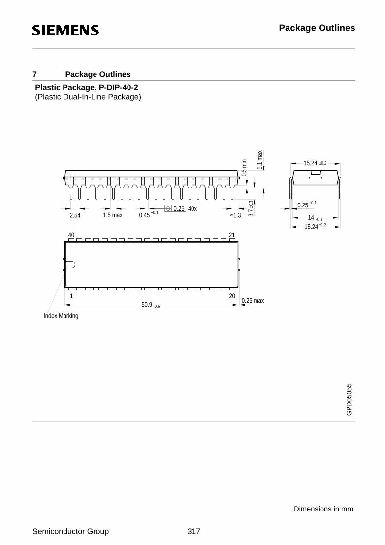
Package Outlines
7 Package Outlines
2.54 1.5 max 0.45 +0.1 1.3 3.7
±0.3
0.5
min
5.1
max
40 21
1 2050.9 -0.5
0.25 max
0.25 +0.1
14 -0.3
15.24 +1.2
15.24 ±0.2
Index Marking
~~0.25 40x
Plastic Package, P-DIP-40-2(Plastic Dual-In-Line Package)
GP
D05
055
Dimensions in mm
Semiconductor Group 317

Package Outlines
Plastic Package, P-LCC-44-1 (SMD)(Plastic-Leaded Chip Carrier)
GP
L051
02
SMD = Surface Mounted Device
Sorts of PackingPackage outlines for tubes, trays etc. are contained in our Data Book “Package Information”
Dimensions in mm
Semiconductor Group 318

Package Outlines
Plastic Package, P-MQFP-64-1 (SMD)(Plastic Metric Quad Flat Package)
GP
M05
250
SMD = Surface Mounted Device
Sorts of PackingPackage outlines for tubes, trays etc. are contained in our Data Book “Package Information”
Dimensions in mm
Semiconductor Group 319
Semiconductor Group 320
Package OutlinesAppendix
Transformers and Crystals Vendor List
Crystals:
Frischer ElectronicSchleifmühlstraße 2D-91054 Erlangen, Germany
KVGWaibstadter Straße 2-4D-74924 Neckarbischofsheim 2, GermanyTel.: (…7263) 648-0
NDK2-21-1 Chome Nishihara Shibuya-KuTokyo 151, JapanTel.: (03)-460-2111orCupertino, CA, USA Tel.: (408) 255-0831
Saronix4010 Transport at San AntonioPalo Alto, CA 94303, USATel.: (415) 856-6900orvia Arthur Behrens KGSchrammelweg 3D-82544 Egling-Neufahrn, Germany
Tele QuarzLandstraße 13D-74924 Neckarbischofsheim 2, Germany
Transformers:
Advanced Power Components (APC)47 RiversideMedway City Estate StroodCounty of Kent, GBTel.: (044) 634-290 588
Pulse EngineeringP.O. Box 12235San Diego, CA 92112, USATel.: (619) 268-2454or4, avenue du QuebécF-91940 Les Ulis, FranceorDunmore Road Tuam County Galway, IrelandTel.: (093) 24107
S+M ComponentsBalanstraße 73P.O. Box 801709D-81617 Munich, GermanyTel.: (…89) 4144-8041Fax.: (…89) 4144-8483
Siemens OostcampBelgium
Schott CorporationSuite 1081838 Elm Hill Pike, Nashville, TN 37210, USATel.: (615) 889-8800
TDKChristinenstraße 25D-40880 Ratingen 1, GermanyTel.: (…2192) 487-0
Universal Microelectronics
Vacuumschmelze (VAC)Grüner Weg 37Postfach 2253D-63412 Hanau 1, GermanyTel.: (…6181) 380or186 Wood Avenue South Iselin, NJ OB830, USATel.: (908) 603 5905
Valor Steinstraße 68D-81667 München, GermanyTel.: (…89) 480 2823Fax.: (…89) 484 743
Vogt electronic AGPostfach 1001D-94128 Obernzell, GermanyTel.: (…8591) 17-0Fax.: (…8591) 17-240


