
IBM of work for IBM. All questions shall be referred to the IBM procurement department requesting a...
28
IBM Engineering Specification: 57G9271 EC: N81528 Page of 28 This specification is property of IBM. Its use is authorized only for responding to a request for quotation or for the performance of work for IBM. All questions shall be referred to the IBM procurement department requesting a quotation or the performance of work. (57G9271 N81528.doc) 1 Package Qualification Guideline Specification Responsible Engineer: C. Grosskopf ([email protected]) Technical Approvals: Actives, Optics, Passives: G. Catucci ([email protected]) Logic CPU: W. Bornstein ([email protected]) Logic Standard: J. Drummond ([email protected]) Memory : L.Dahl ([email protected]) Document Liaison: S.Jumat ([email protected]) Previous EC Level Previous EC Level Previous EC Level Previous EC Level Current EC Level F02220 04-03-01 J90459 05-19-06 J37579 11-14-08 J38428 9-8-11 N81528 04-15-13
Transcript of IBM of work for IBM. All questions shall be referred to the IBM procurement department requesting a...

IBM Engineering Specification: 57G9271 EC: N81528
Page of 28 This specification is property of IBM. Its use is authorized only for responding to a request for quotation or for the performance of work for IBM. All questions shall be referred to the IBM procurement department requesting a quotation or the performance of work. (57G9271 N81528.doc)
1
Package Qualification Guideline Specification
Responsible Engineer: C. Grosskopf ([email protected])
Technical Approvals: Actives, Optics, Passives:
G. Catucci ([email protected])
Logic CPU: W. Bornstein ([email protected])
Logic Standard:
J. Drummond ([email protected])
Memory: L.Dahl ([email protected])
Document Liaison: S.Jumat ([email protected])
Previous EC
Level Previous EC
Level Previous EC
Level Previous EC
Level Current EC
Level F02220
04-03-01 J90459
05-19-06 J37579
11-14-08 J38428 9-8-11
N81528 04-15-13

IBM Engineering Specification: 57G9271 EC: N81528
Page of 28 This specification is property of IBM. Its use is authorized only for responding to a request for quotation or for the performance of work for IBM. All questions shall be referred to the IBM procurement department requesting a quotation or the performance of work. (57G9271 N81528.doc)
2
Table of Contents
Section Section Title Page 1 Scope 3 2 Applicability 3 3 Referenced Documents 3 4 Exceptions 4 5 Testing Requirements 4
5.1 General Requirements for New Qualifications and PCNs 4 5.2 Requirements for Conversions from Gold to Copper (Cu)
Thermosonic Wirebonds 6
6 Test Definitions 7 7 Reliability Tests for Packages 9 8 Reliability Tests, Devices Affected by Second Level Interaction 10 9 Preconditioning 10
10 Fail Handling Procedure for Qualifications 11 11 Tab DIMM Module - Minimum Requirements for Substrate
and Assembly Qualification 12
Appendix A Recommended Preconditioning Flows for PTH (Pin Through Hole) Components
18
Appendix B Recommended Preconditioning Flows for Backside Wave Attach of SMT Components
19
Appendix C Drop Test 20 Appendix D Airflow Susceptibility Test for Copper Wire Bonding 21 Appendix E Audit Checklist for Copper Wire Bonding 24

IBM Engineering Specification: 57G9271 EC: N81528
Page of 28 This specification is property of IBM. Its use is authorized only for responding to a request for quotation or for the performance of work for IBM. All questions shall be referred to the IBM procurement department requesting a quotation or the performance of work. (57G9271 N81528.doc)
3
1. Scope This document defines package and module test requirements for new qualifications, and process changes. To determine the tests required, refer to Sections 5 and 11. Tests are described in Sections 6, 7, 8 and 11. All of the testing requirements of this document need not be performed if an alternate qualification plan has been previously approved by IBM or substitute data is provided to IBM which adequately addresses the identical fail mode. IBM recommends that suppliers develop their internal qualification process using one of the JEDEC qualification methodologies: JESD94 or JESD47, and the following JEDEC publications may also be incorporated: JEP131, JEP143, JEP148, and JEP150.
2. Applicability This entire document, except for Appendix B, is applicable to devices in packages and modules from the memory, logic, power conversion, oscillator, optics, and actives commodities. Appendix B is only applicable for the active commodities. This document is not applicable to other commodities unless specifically called out by another IBM document. 2.1 Terms & Definitions Package - A carrier containing a singular IC (Integrated Chip) that is connected using only first level interconnect. May also include a package with 2 or more ICs, but the package type is primarily used to contain only one IC. A few examples: a PQFP with 2 or more ICs mounted inside it (stacked die, or dual die), a BGA or PGA with on board decoupling capacitors. Module - A carrier containing multiple ICs and possibly passives components that are connected using either first level and/or second level interconnect. Modules are typically socketed or soldered to a larger planar/motherboard. Some examples of modules include: Memory Modules (DIMMs, flash cards, etc.,), MCMs (Multi-Chip Modules), and Board Mounted Power assemblies.
3. Referenced Documents This revision references the following IBM documents and industry standard documents.
Document Number Document Title IBM P/N 0873444 Product Quality Addendum [PQA] For Purchased Electronic Components IBM P/N 77P3021 Additions, Exceptions, and Limitations to Industry Standards to be Applied to IBM
Custom DIMMs IBM P/N 61X5956 Printed Circuit Contact Tab Requirements for Wiping Contacts IBM P/N 21H5140 Test Coupon Design and Impedance Measurement Specification IBM P/N 78P2860 IBM Logic Technology and Component Qualification Guidelines MIL Standard 883 Test Methods and Procedures for Microelectronics JEP 131 Process Failure Mode and Effects Analysis (FMEA) JEP 143 Solid State Reliability Assessment and Qualification Methodologies JEP 148 Reliability Qualification of Semiconductor Devices Based on Physics of Failure
Risk and Opportunity Assessment JEP 150 Stress-Test-Driven Qualification of and Failure Mechanisms Associated with
Assembled Solid State Surface-Mount Components JEP 154 Guideline for Characterizing Solder Bump Electromigration under Constant Current
and Temperature Stress JESD22-A113 Preconditioning of Plastic Surface Mount Devices Prior to Reliability Testing

IBM Engineering Specification: 57G9271 EC: N81528
Page of 28 This specification is property of IBM. Its use is authorized only for responding to a request for quotation or for the performance of work for IBM. All questions shall be referred to the IBM procurement department requesting a quotation or the performance of work. (57G9271 N81528.doc)
4
Document Number Document Title JESD22-A122 Power Cycling JESD22-B116 Wire Bond Shear Test Method JESD 47 Stress-Test-Driven Qualification of Integrated Circuits JESD 69 Information Requirements for the Qualification of Silicon Devices JESD 94 Application Specific Qualification Using Knowledge Based Test Methodology J-STD-020 (IPC & JEDEC)
Moisture/Reflow Sensitivity Classification for Plastic Integrated Circuit Surface Mount Devices
J-STD-035 (IPC & JEDEC) Acoustic Microscopy for Non-Hermetic Encapsulated Electronic Components IPC A-600 Acceptability of Printed Boards IPC TM-650 Test Methods Manual IPC 6012 Qualification and Performance Specification for Rigid Printed Boards IPC SM-840 Qualification and Performance of Permanent Solder Mask
Copyrighted standards are available through many sources, including the following:
Agency (Abbreviation) Name Internet Address IPC http://www.ipc.org/default.aspx
(JEDEC) Joint Electron Device Engineering Council http://www.jedec.org/ (Mil) Military Standard Specifications http://dodssp.daps.dla.mil/
4. Exceptions Any exceptions to the requirements in this document must be approved and documented by the appropriate IBM procurement organization, prior to supplier implementation. Any changes to previous agreements (sample sizes, preconditioning, etc.,) between the component supplier and IBM must be approved by the appropriate technical personnel within IBM procurement. New suppliers must review their qualification process with IBM. This document is IBM's initial request.
5. Testing Requirements 5.1 General Requirements for New Qualifications and PCNs The tests referenced below are described in IBM specifications 0873444 and this document. In the table below, the number(s) or letter(s) following the specification number denote which sections of that specification are required. The introduction to each test describes that test(s), and will determine the applicability of each section within the test to the package being tested. The recommended test sample sizes are as follows: (samples should come from 3 assembly lots)
Total Quantity
Physical outline dimensions which can be affected by handling/shipping 150 pieces All other physical outline dimensions & solderability 15 pieces All other tests where the quantity is not specified in the referenced specification 3 pieces

IBM Engineering Specification: 57G9271 EC: N81528
Page of 28 This specification is property of IBM. Its use is authorized only for responding to a request for quotation or for the performance of work for IBM. All questions shall be referred to the IBM procurement department requesting a quotation or the performance of work. (57G9271 N81528.doc)
5
Affected Packages
Change to Testing Requirement
All Packages and Modules
New Assembly Site, New Assembly Supplier, or New Package/Module Family
0873444 - All of Section 6, except 6.17 57G9271 - S, C, Rel, 2nd L
All Packages New Package (Lead count, body size, lead pitch, etc.) in Previously Qualified Package Family
087344 - 6.3, 6.5, 6.10, 6.13 57G9271 - S, C, Rel
All Packages Any material change that alters the existing environmental material declaration
0873444 – 5.1.1 (Provide access to updated material declaration document)
All Memory Devices and all Logic Devices with Imbedded Memory or Technology Node of 90nm
Any material change that alters the SER (Soft Error Rate) classification for a device - Use of ultra low alpha (ULA) materials for encapsulant, underfill, solder mask, flip chip bump, pre-solder, and SOP (solder on pad)
0873444 – 5.1.3 (Verify emissivity rate of new material is < 0.002 cph/cm2)
All Packages Die Passivation 0873444 - 6.13 57G9271 - 2C, Rel (Rel not required for Hermetic packages)
All Packages Die Coat (including wafer coat) 087344 - 6.5, 6.13 57G9271 - 1C, 2C, 3C, 4C, 7C, Rel (Rel not requirement for Hermetic package)
All Packages Device Thickness and/or Die Thickness or size (area) increase
087344 - 6.5, 6.10, 6.13 57G9271 - 4C
Wirebonded IC
Conversion of thermosonic wirebonder from Au wire to Cu wire. This also covers wirebonder conversion of bonder models and manufacturers, and conversion kits not covered by initial qual
57G9271 – 5.2
Wirebonded IC
Chip Bond Pad Design or Metallurgy, or Bond Pad Diffusion Barrier Metal
0873444 - 6.5, 6.10, 6.13 57G9271 - 1C, 3C, Rel
Flip Chip IC Flip Chip - Under Bump Metallurgy (UBM), Bump Metallurgy and/or Design
0873444 - 6.5, 6.13 57G9271 - EM, 1C, Rel, 2nd L
Flip Chip IC Underfill Material or Process 0873444 - 6.3, 6.5, 6.13 57G9271 - 5C, 6C, 7C, Rel, 2nd L
All Packages Die Backside Metallurgy or Finish 0873444 - 6.5, 6.13 57G9271 - 5C, Rel
Wirebonded IC
Die Attach Adhesive Material or Process 0873444 - 6.5, 6.10, 6.13 57G9271 - 4C, 5C, 7C, 9C, Rel
Leaded Module/Pkgs
Lead/Leadframe Material, Design, or Fabrication Method (i.e., etched vs. stamped)
0873444 - 6.3, 6.4, 6.5, 6.13 57G9271 - 6C, 7C, 8C, 9C, Rel
All Packages Heat Spreader, Heat Slug, Stiffener, and (flip chip) Lid Material or Design
0873444 - 6.3, 6.4, 6.5, 6.13 57G9271 - S, 4C, 6C, 7C, Rel
Flip Chip Pkg w/heatslug
Thermal Interface Material (TIM) change 0873444 - 6.5, 6.13 57G9271 - 12C, Rel – T/C or Power Cycling only
Organic Substrate Pkgs
Organic Substrate Material, Supplier, layer count, or stack up
0873444 - 6.2, 6.3, 6.4, 6.5, 6.9, 6.13 57G9271 - 5C, 6C, 7C, 11C, Rel, 2nd L
Organic Substrate Pkgs
Organic Substrate Pad Design or Metallurgy (incl. solder ball/joint, flip chip, wirebond, and die bond)
0873444 - 6.5, 6.13 57G9271 - 1C, 5C, 7C, 11C, Rel, 2nd L
BGA BGA Solder Ball Material or Composition 0873444 - 6.3, 6.13 57G9271 - 10C, 11C, 2nd L
BGA and PGA
BGA/PGA Passive or Active Component (i.e., decoupling cap.) Value, Supplier, or Number of Devices Used
0873444 - 6.3, 6.6, 6.13 57G9271 - F

IBM Engineering Specification: 57G9271 EC: N81528
Page of 28 This specification is property of IBM. Its use is authorized only for responding to a request for quotation or for the performance of work for IBM. All questions shall be referred to the IBM procurement department requesting a quotation or the performance of work. (57G9271 N81528.doc)
6
Wirebonded Packages and Modules
Bonding Wire Diameter, Material, or Technique 0873444 - 6.5, 6.10, 6.13 57G9271 - 1C, 3C, 4C, Rel High Temp. Storage Test, followed by 1C
Leaded and Leadless Module/Pkgs
External Finish 0873444 - 6.3, 6.4, 6.13 57G9271 - 5C, Rel - THB or HAST only
Plastic Encapsulated
Molding Compound 0873444 – 6.2, 6.3, 6.4, 6.5, 6.9, 6.13 57G9271 - 10C, Rel
Non-Hermetic Module/Pkgs
Moisture Sensitive Class 0873444 - 6.5 57G9271 - S, 1C, 6C, 7C, Rel
Ceramic Module/Pkgs
New Ceramic Manufacturer or Plant 0873444 – 6.2, 6.3, 6.4, 6.5, 6.6, 6.10 57G9271 - 1C, 3C, 4C, 5C, 8C, 9C, 10C, Rel
Ceramic Ceramic/ Seal Material or Method 0873444 - 6.5, 6.10, 6.13 57G9271 - 1C, 3C, 4C, 8C, 9C, 10C, Rel
Ceramic Ceramic Composition 0873444 – 6.2, 6.3, 6.4, 6.5, 6.6, 6.10, 6.13 57G9271 - 3C, 4C, 8C, 9C
Modules Substrate Supplier, Material, Layer Count, Stack-up, via, or imbedded passives
0873444 – 6.2, 6.3, 6.4, 6.9, 6.13, 6.14 57G9271 - 5C, 2nd L
Modules Supplier of or Type of Component(s) in Module, or Physical Layout (components and wiring)
0873444 - 6.3, 6.13 57G9271 - F
Modules Solder Paste Metallurgy, Flux, or Supplier (i.e., change from water soluble to no clean)
0873444 - 6.4, (For pinned cards), 6.13, 6.14 57G9271 - 5C, 2nd L
Modules Component underfill, card encapsulating material, or potting material
0873444 – 6.2, 6.4, 6.5, 6.9, 6.13, 6.14 57G9271 - 5C, 2nd L
Modules Manufacturing Process that is significant. (i.e., point solder automation, card singulation method)
0873444 - 6.3, 6.4, 6.14 57G9271 - 2nd L
All Package Marking Process / Material 0873444 – 6.2 Tape + Reel Tape & Reel Material, Sealing Equipment, or
Hub/Reel Dimensions 0873444 - 6.3 57G9271 - S and Drop Test
All Shipping Tube, Tray, or Clamshell 0873444 - 6.3 57G9271 - S and Drop Test
5.2 Requirements for Conversions from Gold to Copper (Cu) Thermosonic Wirebonds For conversions to copper wirebonds the qualification report is to include the results from the following test requirements: 5.2.1 Mechanical Requirements Line monitor data can be used to support this requirement: Test Sample Size Criteria Wirebond pull test 30 wires/unit from
5 units/lot x 3 lots Force & mode per Mil-std 883 Method 2011.7, Ppk 1.67 or Cpk 1.33 (See Note)
Ball bond shear test 30 ball bonds/unit from 5 units/lot x 3 lots
Force and mode per JESD22-B116, Ppk 1.67 or Cpk 1.33 (See Note)
Bond cratering test (etch bond pads)
20 pads/unit from 5 units/lot x 3 lots No evidence of damage to silicon under bond pads
If the device being qualified has less than 30 wirebonds, increase the number of units to ensure that at least 150 wires/bonds per lot are tested for wire pull and bond shear. If the device being qualified has less than 20 bond pads, increase the number of units to ensure that at least 100 pads per lot are tested for bond cratering.

IBM Engineering Specification: 57G9271 EC: N81528
Page of 28 This specification is property of IBM. Its use is authorized only for responding to a request for quotation or for the performance of work for IBM. All questions shall be referred to the IBM procurement department requesting a quotation or the performance of work. (57G9271 N81528.doc)
7
Note: Process Performance (Ppk) and Process Capability (Cpk) are calculated with the following formula:
3,
3
LSLUSLMin For Ppk, is calculated (estimated) with 1
)(1
2
n
xxn
ii
where individual x’s are used.
For Cpk, is calculated (estimated) within-subgroup variations; e.g., 2d
Ror
4cs
in control charts.
Per JESD47H, use of Cpk should be limited to data on more than 30 lots. 5.2.2 Construction Analysis Requirements The requirements below are in addition to those in section 6.3 of this document for wirebonded packages. 1C - Visual integrity of wire (check for corrosion) and for evidence of bond cratering 3C – Include following additional items for internal inspection: Al splash, bond placement 5.2.3 Reliability Stress Tests Requirements Must meet requirements in Section 7 of this specification, with the following two additional requirements: 1. Wirebond pull and ball bond shear testing at the end of each stress. Pull/shear 10 wires/bonds per unit from 5 units from each of the 3 lots. Force values and mode after stress must meet fail criteria as stated in Mil-std 883 Method 2011.7 for wire bond pull and JESD22-B116 for ball bond shear. 2. Unbiased HAST and unbiased T&H will not be accepted in lieu of biased HAST and/or biased T&H. 5.2.4 Process Audit Requirements As part of qualification report, provide the results of the test described in Appendix D and filled out questionnaire in Appendix E. - Airflow Susceptibility Test for Copper Wire Bonding (Appendix D) - Preaudit checklist/questionnaire (Appendix E) IBM has noted differences in ambient airflow rates around wirebonders as well as transient rates due to human actions. Some conversion kits are able to handles flow rates of 2 m/sec, while others only 1 m/sec. Therefore, all designs and locations need to be evaluated, to ensure that the forming gas will surround the Cu bonding area 100% of the time. Air flow measurements shall be recorded for ambient airflow around the bonding stations. Measurements shall also be recorded for various human induced (transient) airflow rates. Such actions may include, but are not limited to: - an operator walking or running by a bonder, - a large cart being pushed past a bonder, - a clipboard or other rigid object being waived near the bonding head, Identify all possible actions that could occur at your facility and measure the airflow rates created by such actions. The results of the Airflow Susceptibility Test should be reviewed to ensure that high quality bonds will be made for all measured ambient and transient airflow rates.
IBM Engineering Specification: 57G9271 EC: N81528
Page of 28 This specification is property of IBM. Its use is authorized only for responding to a request for quotation or for the performance of work for IBM. All questions shall be referred to the IBM procurement department requesting a quotation or the performance of work. (57G9271 N81528.doc)
8
5.2.5 Additional PCN Requirements for Cu Thermosonic Bonding Prior to implementation, IBM requires that a PCN notice be submitted for any design change to the wire bonding equipment that could impact thermosonic copper wire bondability and/or reliability. Some examples of such changes include: a design change to forming gas nozzles a design change to shielding converting bonders to bond copper wires of another manufacturer or different models from the same
manufacturer after the initial qualification and were not covered by the initial qualification. IBM requires such changes to have been qualified to the same requirements as the initial copper wire qualification and that all qualification documentation be provided to IBM with the PCN notice. NOTE: IBM’s PCN requirements are stated in IBM engineering specification 873444.
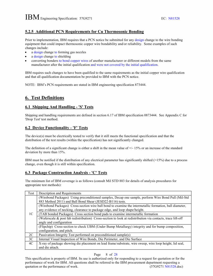
6. Test Definitions 6.1 Shipping And Handling - 'S' Tests Shipping and handling requirements are defined in section 6.17 of IBM specification 0873444. See Appendix C for 'Drop Test' test method. 6.2 Device Functionality - 'F' Tests The device(s) must be electrically tested to verify that it still meets the functional specification and that the distribution of the test results (within the specification) has not significantly changed. The definition of a significant change is either a shift in the mean value of +/- 15% or an increase of the standard deviation by more than 15%. IBM must be notified if the distribution of any electrical parameter has significantly shifted (>15%) due to a process change, even though it is still within specification. 6.3 Package Construction Analysis - 'C' Tests The minimum list of IBM coverage is as follows (consult Mil STD 883 for details of analysis procedures for appropriate test methods):
Test Description and Requirements (Wirebond Packages) Using preconditioned samples, Decap one sample, perform Wire Bond Pull (Mil-Std 883 Method 2011) and Ball Bond Shear (JESD22-B116) tests. (Wirebond Packages) Cross-section wire ball bond to examine the intermetallic formation, ball diameter, any evidence of necking, clearance to package edge, and loop shape/height. (TAB bonded Packages) Cross section bond pads to examine intermetallic formation (Waferscale & post fab redistribution) Cross-section to look at redistribution via contacts, trace lift-off angle and configuration
1C
(Flipchip) Cross-section to check UBM (Under Bump Metallurgy) integrity and for bump composition, configuration, and pitch.
2C Passivation Integrity Test performed on preconditioned sample(s) 3C Internal Visual Inspection of Wire Bonds, Die Perimeter, and Die Surface 4C X-ray of package showing die placement on lead frame/substrate, wire sweep, wire loop height, lid seal,
and die attach.
IBM Engineering Specification: 57G9271 EC: N81528
Page of 28 This specification is property of IBM. Its use is authorized only for responding to a request for quotation or for the performance of work for IBM. All questions shall be referred to the IBM procurement department requesting a quotation or the performance of work. (57G9271 N81528.doc)
9
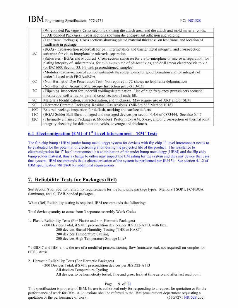
(Wirebonded Packages) Cross sections showing die attach area, and die attach and mold material voids. (TAB bonded Packages) Cross sections showing die encapsulant adhesion and voiding (Leadframe Packages) Cross sections showing plated material thickness' on leadframe and location of leadframe in package (BGAs) Cross-section solderball for ball intermetallics and barrier metal integrity, and cross-section substrate for via-to-interplane or microvia separation (Substrates - BGAs and Modules) Cross-section substrate for via-to-interplane or microvia separation, for plating integrity of substrate via, for minimum pitch of adjacent vias, and drill smear clearance via to via (or IPC 600, Section 33.1-9 with preconditioned samples)
5C
(Modules) Cross-section of component/substrate solder joints for good formation and for integrity of underfill used with FBGA/uBGA.
6C (Non-Hermetic) Dye Penetration Test- Not required if 7C shows no leadframe delamination (Non-Hermetic) Acoustic Microscopy Inspection per J-STD-035
7C (Flipchip) Inspection for underfill voiding/delamination. Use of high frequency (transducer) acoustic microscopy, soft x-ray, or parallel cross-section of underfill.
8C Materials Identification, characterization, and thickness. May require use of XRF and/or SEM 9C (Hermetic Ceramic Packages) Residual Gas Analysis (Mil-Std 883 Method 1018)
10C External package inspection for deflash, marking and surface defects. 11C (BGA) Solder Ball Shear, on aged and non-aged devices per section 6.4.6 of 0873444. See also 6.4.7 12C (Thermally enhanced Packages & Modules) Perform C-SAM, X-ray, and/or cross-section of thermal joint
integrity checking for delamination, voids, coverage and thickness. 6.4 Electromigration (EM) of 1st Level Interconnect - 'EM' Tests The flip chip bump / UBM (under bump metallurgy) system for devices with flip chip 1st level interconnect needs to be evaluated for the potential of electromigration during the projected life of the product. The resistance to electromigration for 1st level interconnect is a combination of the under bump metallurgy (UBM) and the flip chip bump solder material, thus a change to either may impact the EM rating for the system and thus any device that uses that system. IBM recommends that a characterization of the system be performed per JEP154. See section 4.1.2 of IBM specification 78P2860 for additional requirements.
7. Reliability Tests for Packages (Rel) See Section 8 for addition reliability requirements for the following package types: Memory TSOP1, FC-PBGA (laminate), and all TAB-bonded packages. When (Rel) Reliability testing is required, IBM recommends the following: Total device quantity to come from 3 separate assembly Week Codes 1. Plastic Reliability Tests (For Plastic and non-Hermetic Packages) - 600 Devices Total, if SMT, precondition devices per JESD22-A113, with flux. 200 devices Biased Humidity Testing (THB or HAST) 200 devices Temperature Cycling 200 devices High Temperature Storage Life* * JESD47 and IBM allow the use of a modified preconditioning flow (moisture soak not required) on samples for HTSL stress. 2. Hermetic Reliability Tests (For Hermetic Packages) - 200 Devices Total, if SMT, precondition devices per JESD22-A113 All devices Temperature Cycling All devices to be hermeticity tested, fine and gross leak, at time zero and after last read point.
IBM Engineering Specification: 57G9271 EC: N81528
Page of 28 This specification is property of IBM. Its use is authorized only for responding to a request for quotation or for the performance of work for IBM. All questions shall be referred to the IBM procurement department requesting a quotation or the performance of work. (57G9271 N81528.doc)
10
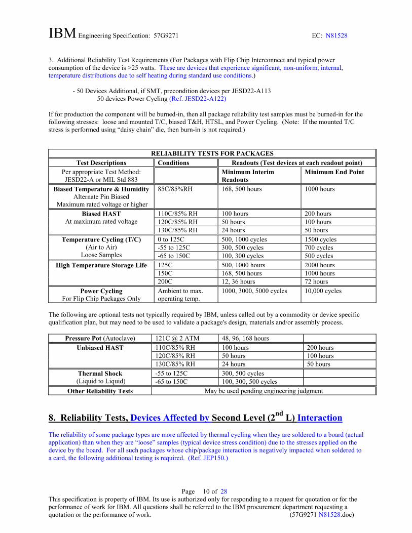
3. Additional Reliability Test Requirements (For Packages with Flip Chip Interconnect and typical power consumption of the device is >25 watts. These are devices that experience significant, non-uniform, internal, temperature distributions due to self heating during standard use conditions.) - 50 Devices Additional, if SMT, precondition devices per JESD22-A113 50 devices Power Cycling (Ref. JESD22-A122) If for production the component will be burned-in, then all package reliability test samples must be burned-in for the following stresses: loose and mounted T/C, biased T&H, HTSL, and Power Cycling. (Note: If the mounted T/C stress is performed using “daisy chain” die, then burn-in is not required.)
RELIABILITY TESTS FOR PACKAGES
Test Descriptions Conditions Readouts (Test devices at each readout point) Per appropriate Test Method: JESD22-A or MIL Std 883
Minimum Interim Readouts
Minimum End Point
Biased Temperature & Humidity Alternate Pin Biased
Maximum rated voltage or higher
85C/85%RH 168, 500 hours 1000 hours
110C/85% RH 100 hours 200 hours 120C/85% RH 50 hours 100 hours
Biased HAST At maximum rated voltage
130C/85% RH 24 hours 50 hours
0 to 125C 500, 1000 cycles 1500 cycles -55 to 125C 300, 500 cycles 700 cycles
Temperature Cycling (T/C) (Air to Air)
Loose Samples -65 to 150C 100, 300 cycles 500 cycles
125C 500, 1000 hours 2000 hours 150C 168, 500 hours 1000 hours
High Temperature Storage Life
200C 12, 36 hours 72 hours
Power Cycling For Flip Chip Packages Only
Ambient to max. operating temp.
1000, 3000, 5000 cycles 10,000 cycles
The following are optional tests not typically required by IBM, unless called out by a commodity or device specific qualification plan, but may need to be used to validate a package's design, materials and/or assembly process.
Pressure Pot (Autoclave) 121C @ 2 ATM 48, 96, 168 hours
110C/85% RH 100 hours 200 hours 120C/85% RH 50 hours 100 hours
Unbiased HAST
130C/85% RH 24 hours 50 hours
-55 to 125C 300, 500 cycles Thermal Shock (Liquid to Liquid) -65 to 150C 100, 300, 500 cycles
Other Reliability Tests May be used pending engineering judgment
8. Reliability Tests, Devices Affected by Second Level (2nd L) Interaction The reliability of some package types are more affected by thermal cycling when they are soldered to a board (actual application) than when they are “loose” samples (typical device stress condition) due to the stresses applied on the device by the board. For all such packages whose chip/package interaction is negatively impacted when soldered to a card, the following additional testing is required. (Ref. JEP150.)

IBM Engineering Specification: 57G9271 EC: N81528
Page of 28 This specification is property of IBM. Its use is authorized only for responding to a request for quotation or for the performance of work for IBM. All questions shall be referred to the IBM procurement department requesting a quotation or the performance of work. (57G9271 N81528.doc)
11
Additionally, new package styles that exhibit a device level coefficient of thermal expansion that are significantly different from industry standard printed circuit boards to the extent that it may not meet 2nd level reliability expectations require the following additional testing. Total device quantity to come from multiple assembly lots, if possible. Packages need to be soldered onto test boards Required for QFN, DFN, TSOP with Alloy42 leadframe, FBGA with ball pitch < 0.8mm, FC-PBGA (organic laminate), and all TAB bonded packages (including uBGA). 100 Devices Total, (may be in lieu of part of the T/C sample size requirement) 100 devices - Mounted Temperature Cycling Devices to be daisy chain mechanical samples with the die being included in the circuit.
RELIABILITY TESTS, SECOND LEVEL
Test Descriptions Conditions Readouts (Test devices at each readout point) Per appropriate Test Method: JESD22-A or MIL Std 883
Minimum Interim Readouts
Minimum End Point
0 to 100C, 2 cycles/hour 300, 500 cycles 1000 cycles -20 to 90C, 2 cycles/hour 300, 500 cycles 1000 cycles -40 to 60C, 2 cycles/hour 300, 500 cycles 1000 cycles
Mounted Temp. Cycling* ** Package soldered to a PCB to
evaluate both Package and Solder Joint Fails
* Minimum 4 layer substrate, 0.062 inch thick. ** For devices intended for double sided applications, this stress should be run double sided.
9. Preconditioning Preconditioning is the simulation of the effects of the board mount soldering process and is performed on devices intended for reliability stress testing. Preconditioning is to be performed per the requirements of JESD22-A113. Flux is required per JESD22-A113. IBM recommends that a highly active, water soluble flux be used. Fluxes with a pH of around 7 (neutral) are not acceptable. Please note that fluxes have low flash points, please use them at the recommended temperatures. Note: Use of acoustic microscopy is highly recommended before and after preconditioning to evaluate package integrity, when applicable. 9.1 IBM Must Be Notified:
Of devices with a moisture classification according to J-STD-020 of 5, 5a, or 6 prior to qualification. Of devices that are not capable of being water washed after card assembly (‘No Clean’ processing only).
See section 6.7.1 in 873444. 9.2 Special Preconditioning Flows If non-standard assembly processes are required, IBM will initiate a request that one of the following Preconditioning flows be performed: 1. Paste in Hole: If PTH product is to be assembled to a card by a convection reflow oven (paste in hole method), it must be evaluated as a Level 1 component per J-STD-020 and preconditioned per JESD22-A113 for SMT product.

IBM Engineering Specification: 57G9271 EC: N81528
Page of 28 This specification is property of IBM. Its use is authorized only for responding to a request for quotation or for the performance of work for IBM. All questions shall be referred to the IBM procurement department requesting a quotation or the performance of work. (57G9271 N81528.doc)
12
2. Backside Wave: If an SMT package is to be qualified for attaching to the backside of a card by immersion into a solder wave, it must be evaluated as a Level 1 component per J-STD-020 at a reflow (classification) temperature of 260C. For preconditioning prior to reliability stress testing, the peak reflow (classification) temperature must also be 260C. See Appendix B for preconditioning flow.
10. Qualification Reports and Fail Handling Procedure for Qualifications IBM recommends that suppliers use JESD69 as the template for the qualification reports they provide to IBM, or integrate all of the reporting requirements stated in JESD69 into their standard qualification reports. Failure analysis must be complete for IBM to consider the Qualification complete. Failure analysis is defined as electrical, hermeticity or visual inspection test diagnosis followed by physical analysis to determine root cause. IBM requires a detailed summary of this information for each failing unit. For data reporting purposes a simple statement of fail mode and root cause is adequate. Below is an example of the recommended format and required information. Stress Test Week
Code Preconditioning 168 hours 500 hours 1000 Hours
THB 85/85, 3.6V bias 9926 0/67 1/67 A 0/66 0/66 THB 85/85, 3.6V bias 9927 0/67 0/67 1/67 C 0/66 THB 85/85, 3.6V bias 9928 0/67 0/67 0/67 0/67
Stress Test Week Code Preconditioning 10 cycles 300 cycles 500 cycles TC (-65 to 150) 9926 0/6 0/67 0/66 (E) 0/67 TC (-65 to 150) 9927 0/67 1/67 B 0/66 0/66 TC (-65 to 150) 9928 0/67 2/67 D & F 0/65 0/65
Fails: A - Ball lift, poor intermetallics B - Ball lift, chip out C - Aluminum pad corrosion, chlorine contamination D - Die corner crack, package stress E - 1 Device removed. Missing ball due to handling during stress testing prevented functional testing. F - Package Fail Fail descriptions A through E are acceptable to IBM. The description for fail F is not acceptable. All fails must be analyzed to determine root cause of failure. A corrective action plan must be in place and approved by IBM Procurement prior to shipment of production product.

IBM Engineering Specification: 57G9271 EC: N81528
Page of 28 This specification is property of IBM. Its use is authorized only for responding to a request for quotation or for the performance of work for IBM. All questions shall be referred to the IBM procurement department requesting a quotation or the performance of work. (57G9271 N81528.doc)
13
11. TAB DIMM - Minimum Requirements for Substrate and Assembly Qualifications 11.1 General
Satisfactory audits of the module and module substrate assembly process are required. A completed IBM DIMM Assembly questionnaire must be provided to IBM. For modules where the JEDEC or IBM designs are modified, substrate designs in .BRD format showing the
stackup must be provided. For new technology elements covered by this qualification, a Failure Mode Effects analysis done according
to JEDEC JEP 131 must be supplied to IBM along with the qualification data. Qualification Hardware Requirements- All hardware shall be of approved subcomponents built on the
production line using production processes. Hardware shall represent as wide a range of vintages of substrate materials, assembly process and subcomponent vintages as possible. At least 2 distinct lots of module substrates, DRAMs, and assembly dates should be used. Different functional Designs may be substituted provided they are equivalent in terms of substrate layer counts, ground rules, materials, and module assembly counts.
Hardware may be reused to satisfy multiple visual requirements. Visual hardware may be reused as functional product or for reliability testing. Reliability test hardware may not be reused.
11.2 Qualification Test Requirements For tables 11.3.1 - 11.3.4, in column 1 ‘Test (When Used)”, tests are identified by number and an alphabetic character. These characters, listed below, define the technology changes which demand that a specific qualification test be performed.
A. New/changed assembly process including DRAM or other device footprint, solder mask or solderable surface finish, solder paste metallurgy, new flux or flux combination (primary and rework fluxes)
B. New/changed DIMM module substrate ground rules (lines and spaces, via size, type, minimum pitch, design, stack up, raw material, laminator, manufacturing process, solder mask or solderable surface finish)
C. Significantly increased assembly process temperature, including lead-free. Qualification is contingent based on completion of testing and satisfactory resolution of any fails.
IBM Engineering Specification: 57G9271 EC: N81528
Page of 28 This specification is property of IBM. Its use is authorized only for responding to a request for quotation or for the performance of work for IBM. All questions shall be referred to the IBM procurement department requesting a quotation or the performance of work. (57G9271 N81528.doc)
14
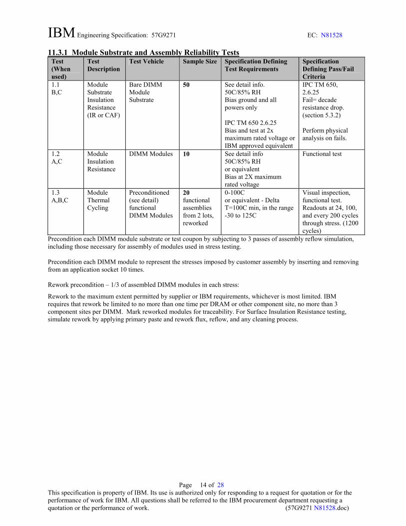
11.3.1 Module Substrate and Assembly Reliability Tests Test (When used)
Test Description
Test Vehicle Sample Size Specification Defining Test Requirements
Specification Defining Pass/Fail Criteria
1.1 B,C
Module Substrate Insulation Resistance (IR or CAF)
Bare DIMM Module Substrate
50 See detail info. 50C/85% RH Bias ground and all powers only IPC TM 650 2.6.25 Bias and test at 2x maximum rated voltage or IBM approved equivalent
IPC TM 650, 2.6.25 Fail= decade resistance drop. (section 5.3.2) Perform physical analysis on fails.
1.2 A,C
Module Insulation Resistance
DIMM Modules 10 See detail info 50C/85% RH or equivalent Bias at 2X maximum rated voltage
Functional test
1.3 A,B,C
Module Thermal Cycling
Preconditioned (see detail) functional DIMM Modules
20 functional assemblies from 2 lots, reworked
0-100C or equivalent - Delta T=100C min, in the range -30 to 125C
Visual inspection, functional test. Readouts at 24, 100, and every 200 cycles through stress. (1200 cycles)
Precondition each DIMM module substrate or test coupon by subjecting to 3 passes of assembly reflow simulation, including those necessary for assembly of modules used in stress testing. Precondition each DIMM module to represent the stresses imposed by customer assembly by inserting and removing from an application socket 10 times. Rework precondition – 1/3 of assembled DIMM modules in each stress:
Rework to the maximum extent permitted by supplier or IBM requirements, whichever is most limited. IBM requires that rework be limited to no more than one time per DRAM or other component site, no more than 3 component sites per DIMM. Mark reworked modules for traceability. For Surface Insulation Resistance testing, simulate rework by applying primary paste and rework flux, reflow, and any cleaning process.

IBM Engineering Specification: 57G9271 EC: N81528
Page of 28 This specification is property of IBM. Its use is authorized only for responding to a request for quotation or for the performance of work for IBM. All questions shall be referred to the IBM procurement department requesting a quotation or the performance of work. (57G9271 N81528.doc)
15
11.3.2 Visual and Finish, Substrate and Assembly Requirements Test (When used)
Test Description
Test Vehicle Sample Size Specification Defining Test Requirements
Specification Defining Pass/Fail Criteria
2.1 A
Assembly visual Including Gold Tab
Assembled DIMM
10 Pieces total 2 lots, 5 pieces from each lot
IBM Physical Outline Drawing, IPC 610 Class 2 * IBM 61X5956 Section 3.5
IBM Physical Outline Drawing, IPC 610 Class 2 * IBM 61X5956, section 3.5
2.2 B
Ni/Au Porosity
DIMM module substrates,
10 Substrates total 2 lots, 5 pieces each
IBM ES 61X5956 Sec 3.3
IBM ES 61X5956, Section 3.3.2
2.3 B
Ni/Au Thickness
DIMM module substrates,
4 Substrates total 2 lots, 2 pieces each
XRF Reference ASTM 568 or equivalent and IBM ES61X5956
IBM ES 61X5956 Section 3.2.1
2.4 A
Module Ionic Cleanliness
Water or solvent clean flux assembled modules only
2 pieces EIA/IPC J-Std 001, EIA/IPC J-Std 001, C-22 clean, contamination < than 1.56 ug/cm2 NaCl equivalent.
2.5 B
Substrate Cleanliness
DIMM module substrates,
4 Substrates total 2 per panel, 2 lots
IPC TM 650, 2.3.25.1 Total ionic contamination< 1.0 ug/cm2 NaCl equivalent.
2.6 B
Substrate Visual Inspection
DIMM module substrates
20 Substrates total 2 lots - 10 pieces
each 4 panels per lot 5 per panel - 4
corners and center
IPC 6012 IBM 61X5956 for Au tabs See Additional Detail
IPC 6012 Class 2 * IBM 61X5956 for Au tabs See Additional Detail
2.7 B
Substrate bow and twist
DIMM module Substrates
4 Substrates total 2 per panel 2 lots
IPC 650 Method 2.4.2.2
IPC 6012C, Section 3.4.3 Neither bow nor twist shall exceed 0.75%
2.8 B
Substrate Micro-section visual, including lay up verification
DIMM module substrates
32 Coupons total 4 per panel on panel corners 4 panels per lot 2 lots
IPC A-600H Sections 3.1.7 3.3.1
IPC A-600H, Sections 3.1.7, 3.3.1 Class 2 * Minimum via wall to voltage plane space 100 uM. (IPC A-600H 3.1.7) See additional detail
2.9 B
Substrate Registration Check visual
IPC Coupons 32 Coupons total 4 per panel on panel corners 4 panels per lot 2 lots
IPC A-600H Sections 3.1.7 3.3.1
IPC A-600H, Sections 3.1.7, 3.3.1 Class 2 * Minimum via wall to voltage plane space 100 uM. (IPC A-600H 3.1.7) See additional detail
2.10 B,C
2X, 6X Solder Float
DIMM module substrates
6 substrates total 2 lots / 1 panel /
lot 3 substrates /
IPC TM 650 Method 2.6.8 d – paragraph 5.4 – 288oC Repeat steps 5.5-5.6,
IPC 6012C Table 3.9. Inner layer separation only.

IBM Engineering Specification: 57G9271 EC: N81528
Page of 28 This specification is property of IBM. Its use is authorized only for responding to a request for quotation or for the performance of work for IBM. All questions shall be referred to the IBM procurement department requesting a quotation or the performance of work. (57G9271 N81528.doc)
16
Panel Diagonal 30
PTHs, 60 connections/ per substrate
6 times No more than 10% of inner layers may show visible separation.
2.11 B,C
2X Solder Float
DIMM Module substrates
6 substrates total 2 lots 3 substrates/lot diagonal
substrates. 30 PTHs, 60
connections/ substrate
IPC TM 650 Method 2.6.8 Repeat steps 5.5-5.6, 2 times.
IPC 6012C Table 3.9 Class 2 * Laminate Integrity -paragraphs 3.6 and 2.6.2.4; Solder mask adhesion – IPC SM-840
* Inspection is to Class 2 requirement, with exceptions listed in 77P3021, “Additions, Exceptions, and Limitations to Industry Standards to be applied to IBM Custom DIMMs”.
11.3.3 DIMM Substrate Electrical Requirements Test (When used)
Test Description
Test Vehicle Sample Size Specification Defining Test Requirements
Specification Defining Pass/Fail Criteria
3.1 B
Impedance Impedance Coupons
20 coupons total 2 lots - 10
coupons each 100 data points
minimum
IBM outline drawing and IBM ES 21H5140
Outline drawing. Test coupons with impedance data to be provided to IBM for correlation. ES 21H5140
3.2 B
Hi pot* DIMM Module Substrates
24 panels total- all substrates 2 lots, 4 panels each from beginning, middle and end of lot.
IPC TM 650 2.5.7,ramp to 550 V, 100V/sec max, hold at max 10 sec. min.
IPC TM 650, 2.5.7. Leakage current < 600 uA See additional detail
* Test is non destructive, parts can be reused for other stress or production
11.3.4 Mechanical Test Requirements
Test (When used)
Test Description
Test Vehicle Sample Size Specification Defining Test Requirements
Specification Defining Pass/Fail Criteria
4.1, A DIMM Module torque
Functional DIMM
2 DIMM modules, 1/lot
See Detail Visual inspection for damage, functional test.
4.2, A Module Impact Shock
Functional DIMM
2 DIMM modules, 1/lot
See Detail See Detail
4.3, A Module Vibration
Functional DIMM
2 DIMM modules, 1/lot
See Detail See Detail
4.4, A, B, C
Solder joint interface integrity
BGA solder joint intermetallic interfaces are prone to brittle failure by various mechanisms depending on construction. A number of standardized and customer specific tests have been developed to control these mechanisms. Describe the tests you use to qualify DIMM assemblies against intermetallic interface failures, and provide data on the performance of your part in these tests.
IBM Engineering Specification: 57G9271 EC: N81528
Page of 28 This specification is property of IBM. Its use is authorized only for responding to a request for quotation or for the performance of work for IBM. All questions shall be referred to the IBM procurement department requesting a quotation or the performance of work. (57G9271 N81528.doc)
17
11.4 Additional Detail
Test 1.1 - DIMM Module Substrate insulation resistance (IR) Testing
The stress setup shall impose bias during stress between the ground network and all power nets.
Stress may be 50, 65, or 85C +/-2C, and 85%RH +/-5% RH,
Bias shall be 2 times the DRAM device application voltage minimum.
Pass/Fail shall be judged at 500 hours. Stress should be continued to 2 times Pass/fail point for information purposes. Readouts to be performed at 24, 48, 100, 150, 200, 300, and 600 hours minimum.. At readouts: Visually inspect for dendritic growth or electrolytic corrosion product.
Report any observed issues as fails.
Test 1.2 - DIMM Module Insulation Resistance
The stress setup shall impose bias during stress between the ground network and all power nets, and as best possible across risk sites, while keeping devices in a low power consumption state, where risk sites are defined as vias at minimum drill pitch. Stress readouts and duration as above, 1.1
Test 1.3 - DIMM Module Thermal Cycling
For equivalent stresses, minimum dwells at extreme temperatures are 7 minutes. Cycle delta T must be of at least 100C in the range -30 to 125C. Stress duration is 1200 cycles at 0 to 100C. Other stresses shall give an equivalent field life using the Coffin mansion equation, equivalent cycles equals 1200 times (delta T (100C) over delta T (proposed)) squared.
Test 2.6 - DIMM Module Substrate Visual For exceptions to IPC 6012 see 77P3021 Test 2.8 - Microsection Visual For exceptions to IPC 6012 see 77P3021 Test 2.9 - DIMM Module Substrate Registration Check visual Registration coupon designs are discussed in IPC-A-600, Section 3.3.1, “Annular Ring - Internal Layers”. The two coupon designs acceptable to IBM are the Coupon F and Coupon R designs discussed in IPC 2221. Coupon F is an x-ray coupon and must be modified to have drilled hole and land sizes representative of what is on the product. Coupon R, which is both an electrical and x-ray coupon, must be modified to have clearance holes in 2 mil increments versus the 20 mil increments shown by IPC. Test 3.2 - HiPot
This test shall be applied between electrically isolated lines, lands, plated through holes, and internal planes.

IBM Engineering Specification: 57G9271 EC: N81528
Page of 28 This specification is property of IBM. Its use is authorized only for responding to a request for quotation or for the performance of work for IBM. All questions shall be referred to the IBM procurement department requesting a quotation or the performance of work. (57G9271 N81528.doc)
18
Test 4.1 - Torque Shock
DIMMs shall be capable of being torqued 1.8o per inch length of the DIMM for 25 cycles. The maximum torque frequency is 0.5 Hertz.
All visible solder joints on the DIMM shall be inspected before and after the test. Any cracking shall be noted.
No fracture of the solder joints after test in excess of 25% of the fillet length is allowed when viewed at 10X magnification.
The DIMM should be verified to be electrically functional at 0oC, 25oC, and 70oC before and after the test.
Test 4.2 - Impact Shock
Mount the DIMM in a typical application socket attached rigidly to an Impact shock table.
Subject the assembly to impact shock 30 G, 25 ms, Trapezoidal pulse, 3 times in each of 3 orthogonal directions, parallel to the major axes of the DIMM module.
Visual, DIMM functional readout post stress.
Test 4.3 - Vibration
Mount DIMM in typical application socket attached rigidly to a vibration table. Scan Vibration over the frequency 20 to 200 Hertz. Identify assembly resonant frequencies in this range.
Dwell 15 minutes vibration at each resonant frequency. Maximum Acceleration to be <0.5G. Visual, DIMM functional readout post stress 11.5 Failure Analysis Any fails occurring during reliability stress testing shall be electrically and physically analyzed to root cause. A report detailing the failure analysis activity shall be provided to IBM, along with any corrective action. 11.6 Coupons Two coupons are discussed in this qualification plan. These coupon types are: 1. Impedance 2. Registration It is IBM’s intent to have the raw card supplier integrate these coupons into the functional panel design, rather than to build unique test vehicle panels. Coupons will therefore have the same cross-section as the functional part being qualified. The impedance and registration coupons are expected to be on the panel at all times, unless the supplier has an equivalent method to demonstrate:
conformance to the impedance specification registration is within specification

IBM Engineering Specification: 57G9271 EC: N81528
Page of 28 This specification is property of IBM. Its use is authorized only for responding to a request for quotation or for the performance of work for IBM. All questions shall be referred to the IBM procurement department requesting a quotation or the performance of work. (57G9271 N81528.doc)
19
Appendix A. Recommended Preconditioning Flows for PTH (Pin Through Hole) Components 1. Temperature Cycle, 5 cycles, -40 to 150C; or similar condition. (Optional) 2. Flux Application - 1, Initial Attach A. Lonco 3355-11 or similar IBM approved highly active, water soluble flux may be used. If Lonco 3355-11 flux is used, it should be used at room ambient temperature and be maintained at a specific gravity of 0.930+/-0.01. The specific gravity may be adjusted by adding isopropyl alcohol. Option 1 Apply flux to the leads by immersing the device in flux. The lead egress area of the package must be completely submerged in the flux. Option 2 If the simulation is to be performed on cards with non-plated through holes or similar vehicle, its thickness shall not exceed 0.065 inches. The components shall be secured to the card using bus-wire or in any other suitable fashion. The card shall be lowered into the flux such that the flux comes up through the holes to the top of the card and completely submerges the lead egress area. The card shall remain in the flux for 2 to 3 seconds. B. Preheat Simulation: Activate flux by heating component to 100C for 30 - 40 seconds. Fixturing must be nonabsorbent and non-contaminating. 3. Wave Solder Simulation Option 1 For preconditioning, immerse leads into solder type specified by IBM: a. SnPb solder at 260C +5/-0C for 5 - 10 seconds b. Pb-free solder at 270C +5/-0C for 7 – 9 seconds Extent of solder immersion should be from lead tip to component standoff. Option 2 If devices are mounted on a printed circuit card, the extent of solder immersion should be to
guarantee contact of solder to the bottom of the card. Solder type and temperature are the same as in Option 1.
FOR PLASTIC PACKAGES STEPS 2-4 SHOULD BE CARRIED OUT IN THE SHORTEST TIME POSSIBLE 4. Within 60 seconds, rinse components in agitated DI water, at 50C minimum, for a minimum of two minutes. 5. Allow devices to dry at room ambient conditions for 10 to 15 minutes. 6. Flux Application - 2, Rework A. Kester 450 or similar IBM approved, activated, water soluble, glycol flux may be used. B. The component shall be immersed in the flux such that the leads and the lead egress area of the package are completely covered with flux. C. This flux must be activated at 120+/-0.5C for 40 - 60 seconds. 7. Repeat step 3 8. Within 60 seconds, rinse components in agitated DI water, at 50C minimum, for a minimum of two minutes. 9. Allow devices to dry at room ambient conditions for 10 to 15 minutes.

IBM Engineering Specification: 57G9271 EC: N81528
Page of 28 This specification is property of IBM. Its use is authorized only for responding to a request for quotation or for the performance of work for IBM. All questions shall be referred to the IBM procurement department requesting a quotation or the performance of work. (57G9271 N81528.doc)
20
Appendix B. Recommended Preconditioning Flows for Backside Wave Attach of SMT Components 1. Temperature Cycle, -65 to 150C, 5 Cycles (Optional) 2. Moisture Soak, 85C / 85% RH for 168 Hours 3. Flux application - 1, Initial Attach A. Lonco 3355-11 or similar IBM approved highly active, water soluble flux may be used. If Lonco 3355-11 flux is used, it should be used at room ambient temperature and be maintained at a specific gravity of 0.930+/-0.01. The specific gravity may be adjusted by adding isopropyl alcohol. B. The component shall be completely immersed in the flux. C. Activate the flux by heating the component to 100C for 30 - 40 seconds before reflow simulation. Move component to reflow immediately. 4. Reflow Simulation - Submerse entire component in molten solder type as specified by IBM: a. SnPb solder at 260C +5/-0C for 5 seconds b. Pb-free solder at 270C +5/-0C for 5 seconds (Component may be wrapped in aluminum foil.) 5. Within 60 seconds, rinse components in agitated DI water, at 50C minimum, for a minimum of two minutes. 6. Flux Application - 2, Rework A. Kester 450 or similar IBM approved, activated, water soluble, glycol flux may be used. B. The component shall be immersed in the flux such that the leads and lead egress area of the package are completely covered with flux. C. This flux must be activated at 120C +/-5C for 40 - 60 seconds. 7. Preheat / Reflow - Repeat step 4. 8. Within 60 seconds, rinse components in agitated DI water, at 50C minimum, for a minimum of two minutes. Note: Preconditioning is now complete. Proceed to appropriate reliability tests.

IBM Engineering Specification: 57G9271 EC: N81528
Page of 28 This specification is property of IBM. Its use is authorized only for responding to a request for quotation or for the performance of work for IBM. All questions shall be referred to the IBM procurement department requesting a quotation or the performance of work. (57G9271 N81528.doc)
21
Appendix C. Drop Test In lieu of an internal or industry standard drop test previously approved by IBM, please perform the following test to ensure the mechanical integrity of components packaged for shipment. 1. Perform automated lead inspection (coplanarity and skew) on all components prior to placement into the shipping media (tray, tape & reel, tube, etc.,). Components are to be serialized. Nonfunctional devices may be used for this test. 2. Package the shipping media into its standard shipping container, as typically loaded for sale to a customer. 3. Perform drop test to the following conditions: Drop Height: 130 cm Number of drops: 10 Orientation of drops: 6 total - On all 6 faces of the shipping box 1 total - On 1 corner 3 total - On each edge adjacent to the above corner 4. Perform visual inspection of shipping container and the shipping media for signs of damage that would inhibit their functional use. 5. Remove the components from the packaging and perform automated lead inspection on all of the components and compare results to initial scan and to package outline specifications. 6. Perform visual inspection on components for any evidence of lead/terminal/ball or package damage.

IBM Engineering Specification: 57G9271 EC: N81528
Page of 28 This specification is property of IBM. Its use is authorized only for responding to a request for quotation or for the performance of work for IBM. All questions shall be referred to the IBM procurement department requesting a quotation or the performance of work. (57G9271 N81528.doc)
22
Appendix D. Airflow Susceptibility Test for Copper Wire Bonding Procedure 1. Preparation A. Fix air gun or equivalent airflow source in front of bonder – shown in Methods 1 and 2 B. Blow air to bonding head and adjust airflow velocity • Levels: 0, 0.5, 1.0, 1.5 and 2.0 m/s C. Measure airflow velocity at multiple points and confirm velocity tolerance of +/-10% throughout FAB forming area of bonding head D. Use hot-wire airflow meter or other equivalent meter to measure above airflow velocity. 2. Pre- test A. Form at least 30 Free Air Balls (FABs) for each of the 5 airflow velocity levels and each of the 3 airflow directions, shown in Method 1/2 and 2/2, and inspect shape and oxidation of FABs. 3. Test A. Bond and sample at least 30 wires from at least 5 units at each of 5 airflow velocity levels from each of 3 airflow directions, shown in Method 1 and 2 for each test B. Measure ball height, ball shear and wire pull strength with observation of destruction modes C. Observe any anomalies on first and second bonds. Airflow Susceptibility Test – Method 1 of 2

IBM Engineering Specification: 57G9271 EC: N81528
Page of 28 This specification is property of IBM. Its use is authorized only for responding to a request for quotation or for the performance of work for IBM. All questions shall be referred to the IBM procurement department requesting a quotation or the performance of work. (57G9271 N81528.doc)
23
Appendix D. Airflow Susceptibility Test for Copper Wire Bonding (cont.) Airflow Susceptibility Test – Method 2 of 2

IBM Engineering Specification: 57G9271 EC: N81528
Page of 28 This specification is property of IBM. Its use is authorized only for responding to a request for quotation or for the performance of work for IBM. All questions shall be referred to the IBM procurement department requesting a quotation or the performance of work. (57G9271 N81528.doc)
24
Appendix D. Airflow Susceptibility Test for Copper Wire Bonding (cont.) Test Report 1. Pre-test result A. Inspection results of FAB shape and oxidation for 5 airflow levels and 3 directions 2. Test result A. Test results for 5 airflow levels and 3 directions for the following measurement and tests 1. Ball height 2. Ball shear strength 3. Wire pull strength B. Above test results to include the following data 1. Average, max and min, and standard deviation (n 30), or all raw data 2. Ppk and spec limits 3. % destruction modes for ball shear and wire pull 4. Any anomalies observed Test Criteria 1. No oxidation or FAB distortion 2. No OOS, Ppk 1.67, no significant change, or no anomalies in A. Ball height B. Ball shear strength C. Wire pull strength 3. Deviations to above criteria need approval by IBM
Note: Process Performance (Ppk) and Process Capability (Cpk) are calculated with the following formula:
3,
3
LSLUSLMin
For Ppk, is calculated (estimated) with 1
)(1
2
n
xxn
ii
where individual x’s are used.
For Cpk, is calculated (estimated) within-subgroup variations; e.g., 2d
Ror
4cs
in control charts.
Per JESD47H, use of Cpk should be limited to data on more than 30 lots.

IBM Engineering Specification: 57G9271 EC: N81528
Page of 28 This specification is property of IBM. Its use is authorized only for responding to a request for quotation or for the performance of work for IBM. All questions shall be referred to the IBM procurement department requesting a quotation or the performance of work. (57G9271 N81528.doc)
25
Appendix E. Audit Checklist for Copper Wire Bonding 1.0 Bonding Equipment 1.1 State bonder manufacturer and model 1.2 State copper wire bonding kit manufacturer and model 1.3 State first bond type (ball or wedge) 1.4 State second bond type (stitch or wedge) 1.5 State bonding stage temperature 1.6 State transducer frequency 1.7 State ultrasonic power 1.8 State bonding force 1.9 State bonding time 1.10 State if bonder automatically stops on non-sticking bonds 1.11 State what procedure is followed once bonder has stopped 1.12 Will thermosonic bonders be converted to use copper wire at a later date (after initial
qualification)? If yes, please answer the following 2 questions: 1.13 State procedure to qualify converted bonders, especially if different models of bonders are to be
converted 1.14 How will customers be notified of conversions initiated after initial qual completed? 2.0 Bonding Capillary 2.1 State capillary material 2.2 State if capillary design is dedicated for copper wire bonding. If yes, state differences from one
for gold wire bonding 2.3 State capillary replacement frequency 2.4 State if capillary can be reworked or cleaned 3.0 Forming Gas 3.1 State incoming gas(es) specs and their tolerances (e.g., N2, H2) 3.2 State gas(es) IQC items 3.3 State forming gas composition spec and tolerance 3.4 State forming gas monitoring items and their action limits at facility area 3.5 State forming gas monitoring items and their action limits at use point 4.0 Forming Gas System 4.1 State flow rate specs with tolerances 4.2 State flow rate action limits and action procedures 4.3 State if bonder automatically stops on out-of-spec flow rate 4.4 State if nozzle alignment spec, adjustment procedure and verification procedure are documented.
If yes, attach the documents. 4.5 State if nozzle PM procedures are documented. If yes, attach the document. 4.6 Attach airflow susceptibility test report (refer to Appendix D) 5.0 Bonding Wire 5.1 State wire manufacturer and type 5.2 State wire metallurgy; (e.g., gold, copper, etc.) 5.3 State wire purity and any alloys/impurities, and if coated, state coating material (e.g., Pd coating
over Cu wire) 5.4 State wire diameter

IBM Engineering Specification: 57G9271 EC: N81528
Page of 28 This specification is property of IBM. Its use is authorized only for responding to a request for quotation or for the performance of work for IBM. All questions shall be referred to the IBM procurement department requesting a quotation or the performance of work. (57G9271 N81528.doc)
26
5.5 State shelf life and storage conditions 5.6 State floor life and storage conditions 5.7 State how Cu wire spool is packed to prevent oxidation 5.8 State Cu wire spool IQC items 5.9 State how wire spool is stored in warehouses 5.10 State temperature/humidity specs of the warehouses 5.11 State shelf life extension period if allowed 5.12 State how wire spool is stored in manufacturing floors 5.13 State temperature/humidity specs of the manufacturing floor 5.14 State how wire spool is released to bonder 5.15 State floor life extension period if allowed 6.0 Die 6.1 State bond pad metallurgy 6.2 State if die is cleaned/processed prior to wire bonding. If yes, respond to the following: 6.3 State how to clean/process 6.4 State smallest pad-to-pad clearance 7.0 Leadframe/Substrate 7.1 State bond area metallurgy 7.2 State if leadframe/substrate is cleaned/processed prior to wire bonding. If yes, respond to the
following: 7.3 State how to clean/processed 8.0 Wire Pull Test 8.1 State if wire pull test performed. If yes, respond to all the following: 8.2 State at which portion of the wire pull force is applied (e.g., 1/3 length from ball) 8.3 State sample size and frequency 8.4 List failure modes if monitored and recorded 8.5 State wire pull test spec limit 8.6 State if control chart is applied. If yes, respond to the following two questions: 8.7 State current control limits 8.8 State if bonder is shut down when pull strength below control limit 8.9 State if bonder is shut down for any failure modes even if the pull force is above spec/control
limit. If yes, respond to the following question: 8.10 List the failure modes 9.0 Stitch/Wedge (second bond) Pull Test 9.1 State if stitch/wedge pull test performed. If yes, respond to all the following: 9.2 State how to perform stitch/wedge (second bond) pull test 9.3 State sample size and frequency 9.4 List failure modes if monitored and recorded 9.5 State wire pull test spec limit 9.6 State if control chart is applied. If yes, respond to the following two questions: 9.7 State current control limits 9.8 State if bonder is shut down when pull strength is below control limit 9.9 State if bonder is shut down for any failure modes even if the pull force is above spec/control
limit. If yes, respond to the following questions: 9.10 List the failure modes

IBM Engineering Specification: 57G9271 EC: N81528
Page of 28 This specification is property of IBM. Its use is authorized only for responding to a request for quotation or for the performance of work for IBM. All questions shall be referred to the IBM procurement department requesting a quotation or the performance of work. (57G9271 N81528.doc)
27
10.0 Ball/Wedge (first bond) Shear Test 10.1 State if ball/wedge (first bond) shear test performed. If yes, respond to all the following: 10.2 State sample size and frequency 10.3 List failure modes if monitored and recorded 10.4 State bond shear force spec limit 10.5 State if control chart is applied. If yes, respond to the following two questions: 10.6 State current control limits for bond shear test 10.7 State if bonder is shut down when shear force below control limit 10.8 State if bonder is shut down for any failure modes even if the shear force is above spec/control
limit. If yes, respond to following question: 10.9 List the failure modes 10.10 For wedge bond, state wedge remnant criteria; i.e., shape, % remaining on bond pad, etc. 11.0 Stitch/Wedge (second bond) Shear Test 11.1 State if stitch/wedge (second bond) shear test performed. If yes, respond to all the following: 11.2 State sample size and frequency 11.3 List failure modes if monitored and recorded 11.4 State wire shear test spec limit 11.5 State if control chart is applied. If yes, respond to the following two: 11.6 State current control limits 11.7 State if bonder is shut down when shear strength below control limit 11.8 State if bonder is shut down for any failure modes even if the shear force is above spec/control
limit. If yes, respond to the following question: 11.9 List the failure modes 11.10 For wedge bond, state wedge remnant criteria; i.e., shape, % remaining on bond area, etc. 12.0 Cratering (chemical etch) Test 12.1 State if bond cratering (chemical etch) is monitored. If yes, respond to the following question: 12.2 State sample size and frequency 13.0 Other Process Control 13.1 State if wire bond rework allowed 13.2 List defects that operators look for at wire bonding station 13.3 State maximum % offset that ball/wedge bond may be off the bond pad 13.4 State if pad metal splash is monitored. If yes, respond to the next three questions: 13.5 State monitoring method for metal splash 13.6 State sample size and frequency for metal splash inspection 13.7 State splash specification 13.8 State if nondestructive wire pull performed. If yes, respond to the following question: 13.9 State pull force for nondestructive pull test 13.10 State if wire loop height is monitored. If yes, respond to the following three questions: 13.11 State monitoring method for wire loop height 13.12 State sample size and frequency for wire loop height inspection 13.13 State wire loop height specification 14.0 Optical Inspection 14.1 State where wire bond inspection (3rd Optical) is performed

IBM Engineering Specification: 57G9271 EC: N81528
Page of 28 This specification is property of IBM. Its use is authorized only for responding to a request for quotation or for the performance of work for IBM. All questions shall be referred to the IBM procurement department requesting a quotation or the performance of work. (57G9271 N81528.doc)
28
14.2 State sample size and frequency 14.3 State defect level (that triggers 100% inspection) 14.4 State magnification 14.5 List defects that device is rejected for 14.6 State how leadframes or substrates are handled for inspection 14.7 State if number of defects are recorded on lot traveler 14.8 State how defective devices are identified and tracked 15.0 On-going Reliability Test 15.1 State if on-gong reliability test for wire bond is performed. If yes, respond to the following two
questions: 15.2 State what tests are performed 15.3 State sample size and frequency


