Transistor fundamentals. Volume 2, Basic transistor circuits
IBM Cur'rent Mode Transistor Logical
Circuits
J. L. WALSH NONMEMBER AlEE
THE CURRENT mode circuits discussed in this paper and in preceding
papers I are intended for use in a very large, high-speed digital computer. From the circuit standpoint, this machine could be classed as a mixed synchronousasynchronous system in which the outputs of chains of logic are often sampled by clock pulses. The system requires circuits which have delays of approximately 20 millimicroseconds per circuit. The basic circuit philosophy discussed
. here is wen suited to the properties of the drift transistor.
Properties of the Transistor
The speed of response of a transistor switching circuit, neglecting stray capacitances, depends on the frequency response and the time constant of base resistancecollector capacitance. Of equal importance is the delay due to minority carrier storage, particularly when this delay approaches the maximum to which one wishes to restrict a circuit. As an example, if one wishes to restrict the circuit delay to 20 millimicroseconds and the saturation delay is 10 millimicroseconds, then only 10 millimicroseconds can be allowed for the transition to the switching threshold of the stages being driven. However, if the saturation delay is e1im-
__ ~--:'-r---;--i-r-t_4._4 mil Iopllmum
170 Me
~MAX. POSSIBLE POWER DISSIPATION
Fig. 1. Drift transistor characteristics
2.45K 240 -5 2.45K 240 .n .n
'6 -12 -6 -12 '6
240 2.45 2 .n .n
Fig. 2. Basic current switches
inated, a full 20 millimicroseconds can be allowed for transition to the switching threshold of the load stages. Clearly, then, a transistor switch operated out of saturation will not have to produce as steep rise or fall times to maintain the same circuit delay as a switch which is driven into saturation.
The frequency response and the collector capacitance are marked functions of the d-c operating point. The situation for a drift transistor is shown in Fig. 1, where curves of constant frequency cutoff and constant collector capacitance are plotted as a function of collector-to-base voltage and collector current. The collector capacitance varies inversely with the 1/3 power of collector voltage, but remains relatively constant .as current is varied over a wide range. The contours of constant frequency cutoff bear some resemblance to a family of rectangular hyperbolas. In general, frequency cutoff increases as collector reverse bias is increased. However, for a fixed value of collector voltage, the frequency cutoff will decrease when the current exceeds the optimum value shown in Fig. 1. Also, the frequency cutoff is poor at very low currents.
The curves of Fig. 1 indicate that when a transistor operates on a load line such as x, frequency response and collector capacitance will approach an optimum within the' hyperbola of allowable power dissipation. The disadvantage of this load line is that, when on, the transistor is required to dissipate more standby power than would be required with a load line that extended into the saturation region.
Basic Current Mode Switch
Consider the basic current mude switches shown in Fig. 2. The circuits are differential amplifiers with one input reference to ground in the p-n-p circuit, and -6.0 volts in the n-p-n circuit. The input signal to the top transistor, T I ,
swings about ground, but only by an amount sufficient to switch current completely into either transistor TI or T2•
In the p-n-p circuit of Fig. 2 the top transistor, T I , is off when the input po-
240n
'0
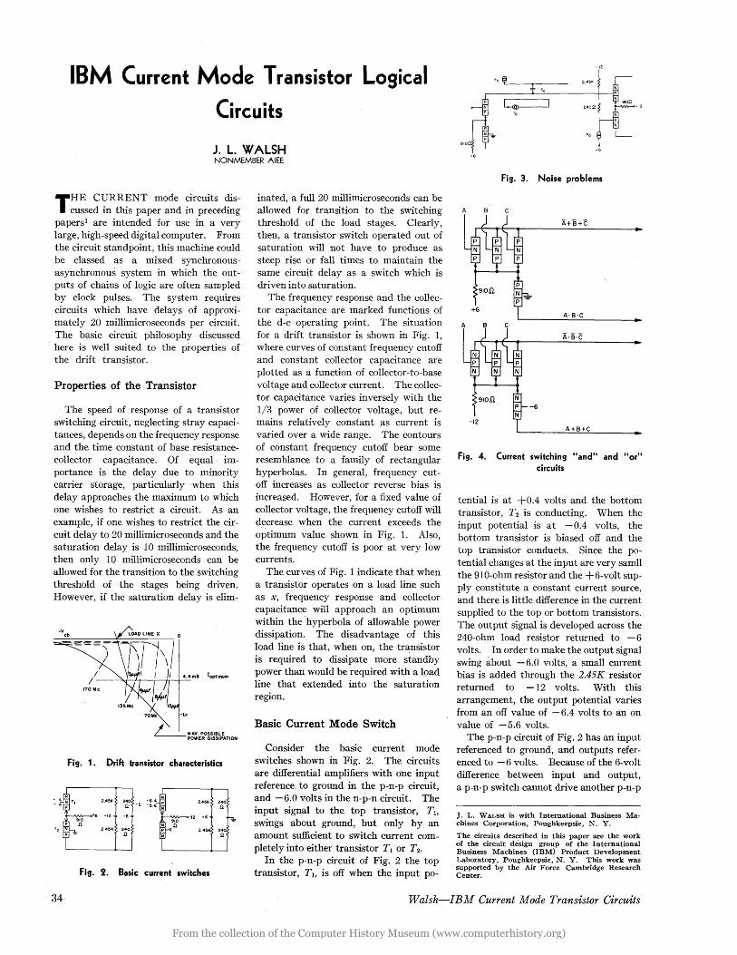
Fig. 3. Noise problems
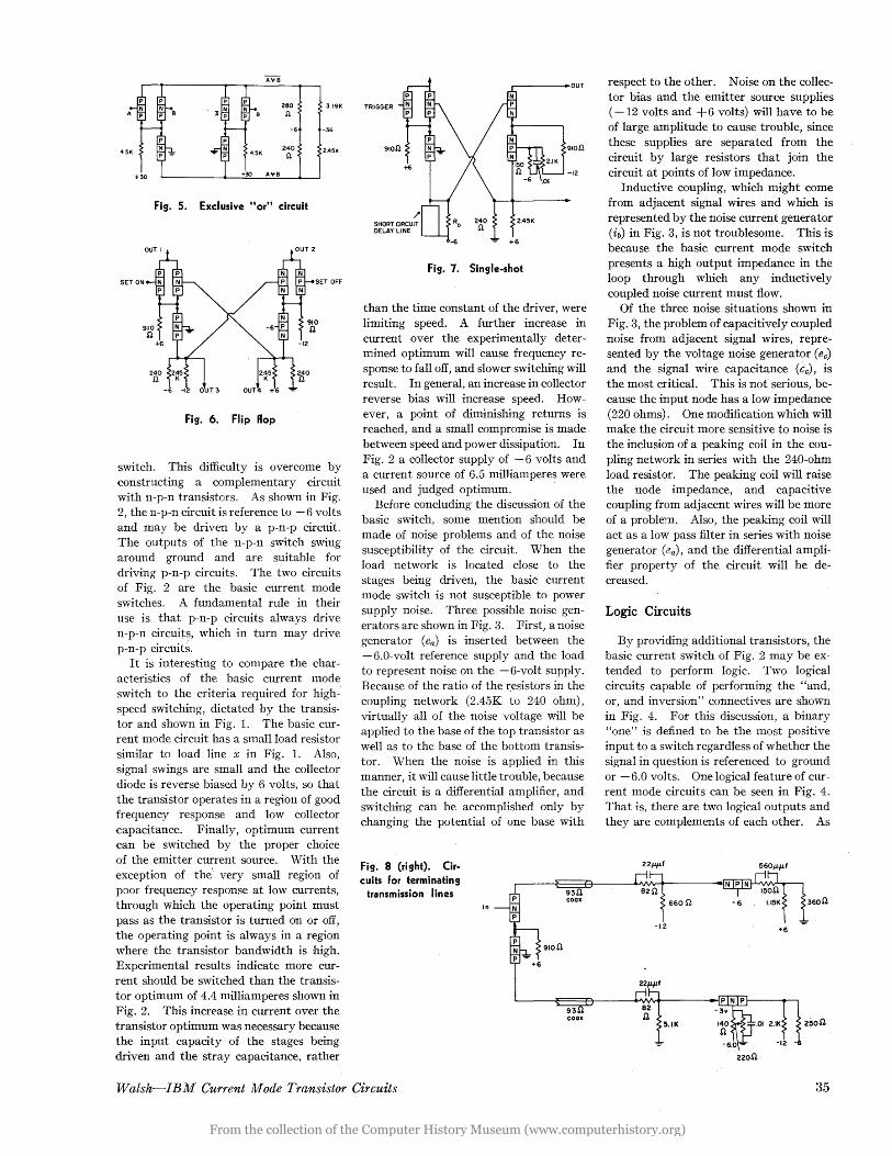
A B c
A·B·C
A'B'C
-6
A+B+C
Fig. 4. Current switching "and" and "or" circuits
tential is at +0.4 volts and the bottom transistor, T2 is conducting. When the input potential is at -0.4 volts, the bottom transistor is biased off and the top transistor conducts. Since the potential changes at the input are very samll the 91O-ohm resistor and the +6-volt supply constitute a constant current source, and there is little difference in the current supplied to the top or bottom transistors. The output signal is developed across the 240-ohm load resistor returned to - 6 volts. In order to make the output signal swing about - 6.0 volts, a small current bias is added through the 2.45K resistor returned to - 12 volts. With this arrangement, the output potential varies from an off value of -6.4 volts to an on value of -5.6 volts.
The p-n-p circuit of Fig. 2 has an input referenced to ground, and outputs referenced to - 6 volts. Because of the 6-volt difference between input and output, a p'-n-p switch cannot drive another p-n-p
J. L_ WALSH is with International Business Machines Corporation, Poughkeepsie, N. Y.
The circuits described in this paper are the work of the circuit design group of the International Business Machines (IBM) Product Development Laboratory. Poughkeepsie, N. Y. This work was supported by the Air Force Cambridge Research Center.
34· Walsh-IBM Current Mode Transistor Circuits
From the collection of the Computer History Museum (www.computerhistory.org)
AYB
280
.u -6
240 .u
Fig. 5. Exclusive "or" circuit
3.19K
-36
2.45K
SET ON SET OFF
Fig. 6. Flip Flop
switch. This difficulty is overcome by constructing a complementary circuit with n-p-n transistors. As shown in Fig. 2, the n-p-n circuit is reference to - 6 volts and may be driven by a p-n-p circuit. The outputs of the n-p-n switch swing around ground and are suitable for driving p-n-p circuits. The two circuits of Fig. 2 are the basic current mode switches. A fundamental rule in their use is that p-n-p circuits always drive n-p-n circuit~, which in turn may drive p-n-p circuits.
It is interesting to compare the characteristics of the basic current mode switch to the criteria required for highspeed switching, dictated by the transistor and shown in Fig. 1. The basic current mode circuit has a small load resistor similar to load line x in Fig. 1. Also, signal swings are small and the collector diode is reverse biase.d by 6 volts, so that the transistor operates in a region of good frequency response and low collector capacitance. Finally, optimum current can be switched by the proper choice of the emitter current source. With the exception of the' very small region of poor frequency response at low currents, through which the operating point must pass as the transistor is turned on or off, the operating point is always in a region where the transistor bandwidth is high. Experimental results indicate more current should be switched than the transistor optimum of 4.4 milliamperes shown in Fig. 2. This increase in current over the transistor optimum was necessary because the input capacity of the stages being driven and the stray capacitance, rather
,-----_OUT
TRIGGER
910n
SHORT CIRCUIT DELAY LINE
910n
-12
2.45K
+6
Fig. 7. Single-shot
than the time constant of the driver, were limiting speed. A further increase in current over the experimentally determined optimum will cause frequency response to fall off, and slower switching will result. In general, an increase in collector reverse bias will increase speed. However, a point of diminishing returns is reached, and a small compromise is made between speed and power dissipation. In Fig. 2 a collector supply of -6 volts and a current source of 6.5 milliamperes were used and judged optimum. '
Before concluding the discussion of the basic switch, some mention should be made of noise problems and of the noise susceptibility of the circuit. When the load network is located close to the stages being driven, the basic current mode switch is not susceptible to power supply noise. Three possible noise generators are shown in Fig. 3. First, a noise generator (ea) is inserted between the - 6.0-volt reference supply and the load to represent noise on the -6-volt supply. Because of the ratio of the r:esistors in the coupling network (2.45K to 240 ohm), virtually all of the noise voltage will be applied to the base of the top transistor as well as to the base of the bottom transistor. When the noise is applied in this manner, it will cause little trouble, because the circuit is a differential amplifier, and switching can be accomplished only by changing the potential of one base with
Fig. 8 (right). Circuits For terminating
transmission lines in
Walsh-IBM Current Mode Transistor Circuits
respect to the other. Noise on the collector bias and the emitter source supplies ( -12 volts and +6 volts) will have to be of large amplitude to cause trouble, since these supplies are separated from the circuit by large resistors that join the circuit at points of low impedance.
Inductive coupling, which might come from adjacent signal wires and which is represented by the noise current generator (ib) in Fig. 3, is not troublesome. This is because the basic current mode switch presents a high output impedance in the loop through which any inductively coupled noise current must flow.
Of the three noise situations shown in Fig. 3, the problem of capacitively coupled noise from adjacent signal wires, represented by the voltage noise generator (ec)
and the signal wire capacitance (cc) , is the most critical. This is not serious, because the input node has a low impedance (220 ohms). One modification which will make the circuit more sensitive to noise is the inclusion of a peaking coil in the coupling network in series with the 240-ohm load resistor. The peaking coil will raise the node impedance, and capacitive coupling from adjacent wires will be more of a problem. Also, the peaking coil will act as a low pass filter in series with noise generator (ea) , and the differential amplifier property of the circuit will be decreased.
Logic Circuits
By providing additional transistors, the basic current switch of Fig. 2 may be extended to perform logic. Two logical circuits capable of performing the "and, or, and inversion" connectives are shown in Fig. 4. For this discussion, a binary "one" is defined to be the most positive input to a switch regardless of whether the signal in question is referenced to ground or - 6.0 volts. One logical feature of current mode circuits can be seen in Fig. 4. That is, there are two logical outputs and they are complements of each other. As
+6
,01 2.1K 250.0.
-12 -
3.5
From the collection of the Computer History Museum (www.computerhistory.org)
a logical"one" is defined here, the top outputs are inverted and the bottom outputs are normal. The fact that inverted outputs are always available eliminates the need for a separate inverter building block in a system. In a long chain of logic where inversion is frequently required, the result is a reduction in over-all delay.
The two logical circuits of Fig. 4 will generate the necessary logical connectives required in a system. However, a separate "exclusive or" building block would be an advantage, since three of the logical blocks of Fig. 4 would be required to generate the "exclusive or" statement and also there would be a delay of two logical blocks in cascade involved. The simple arrangement of logical blocks shown in Fig. 5 will generate an "exclusive or" statement with a delay of only one logical block. Only the p-n-p version of the circuit is shown, but the n-p-n version can be formed in a similar manner. The "exclusive or" circuit consists of two parallel "and" circuits which generate A·R and A·B. With the four inputs connected as shown, only one of the "and" circuit outputs can be conducting at anyone time. Therefore, the "and" circuit outputs can be connected to form the "or"- circuit required to complete the "exclusive or" function. Under the input conditions l·B or A·B, the inverted outputs of both "and" circuits will be conducting and two units of current will flow into the load network. This network is designed to give a normal output only when both sides are conducting, and in this manner the inverted "exclusive or" statement is obtained. The inverted outputs will supply only one unit of current when the normal "exclusive or" inputs (A-:B+ A·B) are present. However, because of the special coupling network, the output signal will not be large enough to switch the load stages. The "exclusive or" circuit requires both the normal and complemented input signals .. This is no problem, .since both normal and complemented outputs will always be available from the driving sources.
No discussion of a set of switching circuits for a computer would be complete
36
without reference to some means of storage and some means of generating a welldefined pulse. The storage circuit in this case is shown in Fig. 6. It consists of two basic switches cross-coupled to form a symmetrical bistable flip-flop. The flipflop can be set in either position through the pull-over transistors on either side. An "or" function can be built into the flip-flop by paralleling the pull-over transistors. Operation is in no way different from the logical block circuits of Fig. 4, previously described.
A basic current mode single-shot is shown "in Fig. 7. The circuit again consists of two basic switches cross-coupled together, but in this case one side is through a short-circuited delay line. The bottom n-p-n transistor is biased off by the network at its base. The shortcircuited delay line is terminated at the sending end, and the pulse width at the output is determined almost entirely by the time required for the wave front at the delay line input to travel down and then back up the delay line.
In any computing systems, situations are encountered where it is necessary to drive loads located at a considerable distance from the driving source. This may be done by driving conventional coaxial transmission line and terminating the coaxial line with either of the circuits shown in Fig. 8. Both the arrangements shown here are driven by a basic current switch. The n-p-n line terminator at the top of Fig. 8 is a Class A grounded-base amplifier. When the top output of the basic switch driving the line is off, the n-p-n transistor conducts and approximately 6.5 milliamperes flow into the current sink formed by the 660-ohm resistor and the -12.0-volt supply. When the top transistor conducts, the emitter current of the n-p-n grounded-base stage is reduced to 0.5 milliampere. The input impedance of this stage has a small inductive component and an impedance of 11 ohms. The 82-ohm resistor is added to increase the total impedance to 93 ohms and match the characteristic impedance of the coaxial line. The small capacitor compensates for the inductive
input component. The value of the series resistance can be changed to match lines of different characteristic impedance if desired. The p-n-p line terminator at the bottom of Fig. 8 operates in the same manner. In this circuit the base is biased to - 3.0 volts so that the output signal will be referenced to - 6.0 volts. The n-p-n circuit differs from the p-n-p circuit in that it translates the output of the bask p-n-p switch from -6.0 volts up to ground level. Because of this, the n-p-n grounded base amplifier can also be used as a coupling means between two p-n-p logical blocks.
In concluding the discussion of the basic circuits, reference should be made to the component tolerances used in the design and the speed of operation that has been achieved with these circuits. Some design information will now be summarized.
Power supplies .. ±4% Resistors ........ ±3% Transistors ...... {3 = 20
Emitter base
70 megacycles 5:.fco 5:.150 megacycles
5 micromicrofarad 5:. Gte 5:. 15 micromicrofarad
40 ohms 5:. rbb 5:. 80 ohms
breakdown .... > 2.5 volts
Circuit delays range from 6.0 to 22 millimicroseconds, the longer delays being associated with the larger loads. The basic logical block is designed to have a fan-out of 3 bases. The number of logical inputs is dependent on the number of loads. Maximum inputs are: 6 inputs for a load of three bases, 8 inputs for a load of two bases, and 10 inputs for a load of 1 base. In general, circuit delays are a function of the load and are not greatly affected by the number of logical inputs.
References
1. MILLIMICROSECOND TRANSISTOR CURRENT SWITCHING CIRCUITS, H. S. Yourke. Proceedings, IRE-AlEE Conference on Transistor and Solid State Circuits, Philadelphia, Pa., Feb. 1957.
2. HIGH SPEED TRANSISTOR COMPUTER CIRCUIT DESIGN, R. A. Henle. Proceedings Eastern Joint Computer Conference, AlEE Special Publication T-92, Dec. 1956, pp. 64-66!
Walsh-"-IBM Current Mode Transistor Circuits
From the collection of the Computer History Museum (www.computerhistory.org)

Discussion
T. R. Finch: The selection of a logical circuit for digital systems reminds me, in some aspects, of the procedure that a family goes through in selecting trees for the new one-acre lot. The house is located on a very barren plot, and since they would . like to enhance their investment, they decide to buy some trees, and, of course, they want to get their money's worth. Well, they can invest in some evergreens which are very glamorous and present a very spectacular show above ground. Depending on where they live and the climate, in a number of years they may be able to call their little one-acre plot their dream place. However, they had better give some serious consideration to the root structure and soil as well as to the glamor above ground if they are indeed to enhance their investment.
I think to a certain extent the design of large-scale systems involves similar problems. It is fun to design a glamorous circuit with many storage elements. Sometimes we cannot understand exactly how they operate, but they operate like a "whizzbang."
Companies that have been in the computer business for a long time, have to balance off system requirements and bring into being a system that has system efficacy. If there is available a whizz-bang system control and calculator that operates at 100-megacycles but must stand around for an hour and wait for the peripheral equipment to perform its data-processing task, then the system efficacy and low cost are most likely imaginary. What we are interested in is the integrated job of reliability at the least cost.
Transistor resistor logic (TRL) is not a glamorous circuit, it is just a "work-horse" circuit that gives you a great deal for your money. I think that the TRL circuit designer lives up to his responsibility of providing a basic circuit that can be understood, has a certain amount of flexibility, and provides the speed that is required across a rather flexible speed range. With TRL, and presently available transistor, is available, propagation time of the order of a tenth of a microsecond. It will not do this with all logical flexibility in all cases, but it is often more advantageous to exchange logical capabilities for the speed needed at lowest cost.
Another point on which I would like to comment is how we· view the use of the transistor as a logical element as opposed to the use of another device in this application. This choice depends upon the size of the system, reliability, and cost principally. (We believe that in the end almost all characteristics, including reliability, have to be priced out.)
At this meeting we have seen circuits which use transistors for logical input, other circuits which use diodes for logical input, and TRL which uses resistors for logical input. We believe that resistors, given the same selection that semiconductors will be given, wlll prove more reliable and more economical and will justify their use wherever speed is not completely dominant.
My basic conte~tion is that people who are using transistors for each logical input are indulging in "rich living," and they have got to get something out of it. What do you
get out of it? In current mode switching you get speed. With direct coupled transistor logic (DCTL), you get simplicity and I contend that at the present time this is not enough to offset stiff transistor requirements and inadequate protection against sporadic error. However, I think that DCTL should be commended; it has been a real catalyst since its circuit simplicity has triggered us toward the evolution of digital systems employing simple logical circuits. I think now is the time to leave DCTL because of the problems related to the severe requirements on the transistors. As time goes on, these severe requirements are. going to keep the DCTL transistor higher priced than the moderate requirements on other systems, and because the transistor is used for logical input it is going to be an expensive system.
In TRL, I think that there is a balance, a flexible balance, that permits the logical designer to meet the system's engineering needs. A study has been made to determine the efficacy of a complete intergrated system that places speed requirements on various blocks, sorters, and calculators, input-output stores, etc., and the study resulted in a group of requirements on logical speed. Once the speed requirements on the circuit are set, what do you want to optimize? The answer is the economics because reliability, maintenance, and the first cost of design ability all are priced out.
The design of TRL circuits is flexible and permits a variety of speeds. Given a year or two, the diffusion-type devices are going to move the alloys out of business, and you will be able to obtain, for the same amount of money, diffusion-type devices of highspeed low-capacity reproducibility and reliability. Our premise in TRL is that it is a good bet to take advantage of what is going to be offered.
As to our thinking in regard to bringing a system into being a couple of years from now, we are betting on the diffusion-type devices with a simple circuit that we can understand and design, and can use in large numbers. We can realize our speed requirements, and we can obtain the various economics from the simple circuit by just scaling the impedance level up or down. This gives us the desired amount of protection against malfunction. If we want to go to higher speed we just lower the impedance level at the inner-stage, and we get high speed with some sacrifice of logical rules, or else we have to use more power.
Our premise again is that d-c power, as it has been refined throughout the years, is the best buy that you can get. You should invest in d-c power in many cases, although this is not true for air-borne applications. I think, if you wanted to design restricted, small scale special-purpose air-borne computers, you would get most value from carefully designed DCTL circuits: low power, low power consumption, and operation on low voltage.
I do not think that I would use TRL if I had a real time problem on a time-sharing basis where I had to get down to millimicroseconds. I do not know what I would use for sure, but I might just have to use some of the transistor rich living I mentioned. I have great confidence in the performance of diffused junction transistors, and I am not afraid to use them, but I do think that it is going to be some time before they are as
Discussion~Logical Circuitry for Transistor Computers
cheap and as reliable as resistors. Webelieve the same is true for diodes. With the same care and attention given to the fabrication of all devices, I think that the resistor is going to outrun the diode and transist0r for a long time to come.
JamesB. Angell: I have one disadvantage in arguing with Mr. Finch, in that basically I am speaking of DCTL predicated on experience. This is not just new and glamorous; . we have had experience with it. So, to some extent what he, and I and others, in fact, will say about DCTL must be based on a fair amount both of design and actual usage and experience.
Before I go on with other comments, I would first like to augment to some extent the question of cost consideration that Mr. Finch started. This is that it is not really the cost per logical element which is of primary consideration in any computer, but it is rather the cost of, or per, logical decision. Certainly there are some cases where there are real time problems with a time scale of doing decisions sufficiently slow so that we are not primarily concerned with how many computations you can do per second. I t is true throughout the majority of cases, if you can do the job faster, you can do it with fewer elements. You are not necessarily going to come out with the conclusion that DCTL is the right answer. I merely wish to augment Mr. Finch's thought.
What is the primary concern? What does it cost to make a given decision? DCTL is certainly not one of the faster types of circuit. It is roughly comparable in speed with what is called resistor-capacitor coupled transistor logic (RCTL), I believe.
This brings us to another point regarding cost. At least in the case of a limited number of machines a very strong factor in the cost is the designability of the circuit. That is, how easy it is to go from paper designs up to the final layout of the machine. I do not know this fact in the case of transistor resistor logic, but in DCTL I know that it is relatively straightforward. This circuitry can be compared almost to a relay logic circuit when you consider each relay to be of monopole, monothrow arrangement; the transistor is single-pole, single-throw relay, with, unfortunately, a connection between input and output. Nevertheless, the transformation. from original layout to final machine is relatively straightforward once the origina:t layout has been designed on the basis of simple logical rules.
Again with regard to cost, to do a given job in a given length of time with the slowest circuits will require more total circuits, and it has been found by experience with DCTL, and in various other cases, that reliability is not only on the basis of components, but also on the basis of intercoimection of the components. How many nodes you have .in the circuit becomes quite important; the total numbet: of contacts, the total number of gadgets, if you will, that you can put in conveniently on a given panel. I add this point to indicate the fact that there is indeed something to be considered not only from the standpoint of a minimum number of circuits, but also for doing a given job in a given length of time.
Another factor to be considered is that of minimum component count. Minimizing the number of costly components does not
37
From the collection of the Computer History Museum (www.computerhistory.org)
necessarily make for minimum over-all cost. It has been experienced and stated by one of the organizations that has been involved with DCTL that the over-all cost of a DCTL machine is not much more than the cost of an RCTL machine of equivalent capacity. Furthermore, it will require less design time because of the simplicity of the design and the smaller number of actual component values that must be determined.
Finally, I would like to leave you with the thought that the logic described by Mr. Walsh is a complementary version of DCTL, in that both use transistor logic.
R .. H. Baker: I do not think that basically there is any difference between the circuitry that we can argue about, but for the sake of discussion I will make comments about each.
First of all, let me consider my own circuitry. On one hand the cost of the components is expensive, but on the other hand if we estimate 75 man-years for doing a job we save 30 kilo-dollars per man year, which is about what one does in a research laboratory. Then this is more than the total cost of all the parts of the machine that we were to build, and for this research job I do not see how we could have done it any other way. Our goal here is to build something for a system evaluation. I do think, however, that the cost of the components will go down, and that this circuitry of ours will become simpler and cheaper. It does have a high-performance record, and as time goes on it can be made simpler.
Now I would like to ask a question about TRL. To show no favoritism I will agree that resistors are more reliable than diodes, and if you can say that reliability is measured by how much per cent something changes, then a resistor changes less percentagewise than a diode does. On the other hand, there is a real question with the greater variation that you can stand with the diode than you can with the resistor because the latter does consume part of the margin of linear device. I am not at all sure that, with the greater allowable variation of diodes, that resistors offer a truly more reliable way. I also say that a hermetically sealeq resistor (but it would be expensive) would be very effective.
I also want to point out that the designs of a paper machine are nothing like getting a machine to work. I think that some of the transient problems are the ones that are going to be really hard to solve, not the d-c problems in TRL. The problem is: One has a machine designed on paper, and you build it up and run a program through it to see if certain parts of the program make errors. This is usually the type of error where you must allow yourself enough flexibility to overcome the difficulties once you have started running the machine, transient-wise.
With regard to DCTL, I just cannot believe that a 3-terminal device is going to be as reliable as a 2-terminal device. I think the diode is more reliable than a transi 3tor because a diode is governed more by a bulk phenomenon than is a transistor, hence,. the transistor is more amenable to surface conditions affecting it than is a diode.
I think that the same comment is true of the' circuitry described by Mr. Walsh. I think that a diode per logical input is eX7
38
pensive. On the other hand, I do not think that he expects this to last very long. In our position, we do not have to have something planned 5 years ahead, and this is where we differ basically from IBM, where the use is commer~jal as well as military. I think that by the 'time we go to his type of logic there will probably be something out with a little faster speed which will put diode logical input out of business. I think that it will probably 'be a p-n-p-n type of device produced by companies such as Radio Corporation of America, with three and four leads.
J. L. Walsh: I find it hard to speak in rebuttal since our problems are different than, for instance, the areas in which Mr. Finch operates. I have no argument with resistor logic, and I can certainly see that in many slow-speed applications it is economically worthwhile.
The advent of the drift transistor has opened up new areas of real high-speed operations, and here I do feel that saturation techniques will not be adequate. We will not in the future be able to neglect the ultimate storage delay which might be 5 or 4 or 3 millimicroseconds.
Chairman Felker: I have a series of questions to present to our speakers. The first question comes from E. J. Gauss, University of California in Los Angeles, for Mr. Finch: "Could not a gain in speed be obtained by the use of diode clamps to limit swings, and thus prevent saturation?"
T. R. Finch: Yes. This is a common way to operate and to use more power and what I call a "speed-up configuration." I commented on this when I pointed out that for a large number of applications falling in the fields of industrial control or business automation, the basic simple circuits with modern-day junction transistors will meet speed-up requirements without resorting to clamps for nonsaturation arrangements.
Chairman Felker: The next question is also from Mr. Gauss, for Mr. Angell: "Could not the "hogging" of current by one of several paralleled bases be minimized by the use of series resistors?"
James B. Angell: First of all, to minimize hogging, the manufacturers of transistors put in what is called "a base spreading resistance." This is not very well controlled, and indeed it has had some effect.
. On the question of hogging, it is fairly stable with time so that if you have a transistor that meets the specifications initially, it will continue to meet that characteristic, not one of age. Second, to add such a base resistance does indeed slow down the turnoff of the transistor. If you will recall Fig.1 of my paper, when the first transistor is activated the second one is supposed to go off. The higher the base resistance of the transistor going off, the slower it turns off, until eventually it gets as bad as TRL. Of course, by adding the resistor you are adding an additional node. Experience has shown in general that when a circuit has relied on transistors to avoid hogging, it has been adequately successful, at least to date.
T. R. Finch: I wish to comment on Mr. Baker's comparison of DCTL to a degenerate design of TRL. This is definitely not
the case because the big problem of DCTL is in its lack of adequate protection against malfunction resulting from a forward-biased "off" transistor, which is one of the strong differences between DCTL and TRL.
Chairman Felker: From A. Wennstron. Hughes Aircraft, for Mr. Baker: "Is diode recovery a serious problem in your highspeed circuits? What diode type do you use?"
R. H. Baker: Yes, it is a problem. However, I would like to point out that one manufacturer is now making a fairly fast diode. Although it was not meant to be particularly fast, if you are really after speed, you can get a diode made in the laboratory within a year that will have recovery time in the order of a millimicrosecond.
Chairman Felker: This question is addressed to Mr. Baker and Mr. Walsh, from S. Disson, Burroughs: "Please comment on pulse propagation problems in circuits with 5- to 50-millimicroseconds stage-delay characteristics, particularly on when and why coax is necessary. Also would Mr. Baker please comment on susceptibility of his circuits to coupled noise?"
J. L. Walsh: I think we gain when we use coaxial for <;able that goes beyond 3 feet; below that, down to 8 inches, we use twisted wire. Beyond that, as far as propagation time, you have to keep track of the delay in the coaxial cable.
R. H. Baker: We do not know the answer to this question; this is what we are working on. We have a feeling that coax is not the answer because it makes the machine too big. It seems to me that if you are going to make the machine run fast, it is going to have to be small to keep the propagation time down. The only way to do this, I think, is to invent a new package where everything stays close to the ground plane. I do not think that there is a simple, general solution to this. All that I can say at the present time is that we have potential designs, and we are trying to get a solution.
Chairman Felker: This is for each panel .. ist, and is from J. C. Hawkins, AL W AC: "Mr. Baker gave a component count figure of 20,000 transistors and 40,000 diodes for one machine. Would other panelists comment on, or estimate the number of components required for typical general-purpose computers using the type of circuits described?"
T. R. Finch: We made a comparison for a part of our system using about 7,500 TRL circuits. The difficulty here is that we worked to the needs of a system, an engineering analysis of what the blocks had to do in the way of terminal speed, if we came up with a solution that was faster it had little value unless the component count was reduced. The prime, dominant characteristic of Mr. Baker's circuit is to use more components to get speed. Also, Mr. Walsh's circuits are more complex than ours, so the comparison was made with DCTL. From our analysis it looked as if DCTL ran from 21/2 to 1 greater in transistor count, and counting joints and cost placed on resistors and transistors. Our estimate for the block, as of 1958 and of 1962 both, was that the
Discussion-Logical Circuitry for Transistor Computers
From the collection of the Computer History Museum (www.computerhistory.org)
TRL was 21/2 to. 1 less expensive far the same speed perfarmance in the black.
Chairman Felker: Mr. Hawkins asks, "I believe that yaustated that yau had 34,000 transistars. Haw much wauld that be?
T. R. Finch: Twenty thausand transistars, and no. appreciable number af diades, and we are averaging abaut five resistars per transistar.
Chairman Felker: Do. yau have so.me figures an that, Mr. Walsh?
J. L. Walsh: I wauld nat care to. campare numbers with numbers used in TRL machines, as campared with the ather numbers discussed here. Frankly, the camparisan wauld be relatively favarable, but I do. nat think that the machines were designed to. do. the same jab. I think it wauld be quite meaningless to. paintout what arder af numbers has been used in TRL machines.
Chairman Felker: Here is a questian fram D. Weisser, IBM, far Mr. Baker: "Do. yau make any effart to. select transistars far minimum minarity carrier starage?"
R. H. Baker: The answer to. this is, "Na." With later-type transistars that we are warking with naw, storageisptactically nanexistent.
Chairman Felker: We naw have a questian pased to. all speakers fram Lauis Kurkjian, Hughes Aircraft: "Which af the 4 systems described are mare applicable to. synchranaus and asynchranaus aperatian?"
J. L. Walsh: I think that the system I described is applicable to. either synchranaus ar asynchronaus aperatian, but certainly there is less af a problem at high speed if yau run equipment as synchranaus.
Chairman Felker: I do. nat see why any af these circuits cauld nat be used in bath types af machines.
James B. Angell: DCTL is used almast campletely in asynchranaus machines.
T. R. Finch: All systems samewhere must be synchranized. As far as TRL is cancerned, yau wait far it to. prapagate and set up an registers, and then it is clacked aut.
Chairman Felker: R. K. Richards, CansuIting Engineer, asks af an speakers: "With all the virtues af the transistar circuits yau have described, how do. yau accaunt far the fact that existing tube camputers are nat experiencing campetitian fram carrespanding transistar camputers?"
J; L. Walsh: I wauld be happy tO,answer that ane. The existing tube camputers are nat really campetitive fram the stand paint af the ultimate use to be achieved. I think that mast peaple are nat designing replacements, but rather are designing equipment to. do. ather bigger jabs faster.
Chairman Felker: The fact is that every-
one is planning a transistar camputer. I, do nat believe anyane is planning new vacuum-tube machines. I would expect' that in 5 years mast af the camputers will be transistar based. In the military field transistars have pretty well wan aut campetitively.
James B. Angell: There is no. daubt abaut it.
J. L. Walsh: I wauld like to. make anather camment an that fact. Until we get a vacuum tube that has a diade drap equal to. the diade drap af the transistars, I think that the transistar will be pretty difficult to. beat far high-speed aperatian.
T. R. Finch: There is a camment I wauld like to. add. I t is difficult to. supersede quickly a system implementatian that has been refined far aver 40 years.
Chairman Felker: This next questian carnes fram 0. S. Gada, Callins Radio. Campany, and is addressed to. Mr. Finch: "Transistars 2N393 and 2N501 are relatively expensive devices at $7.50. Haw do. yau justify ecanamy when 0.25-micrasecand propagatian time is obtainable with a diode oR-transistor NOT circuit using allay-junctian 8-megacycle, $1.50 transistor?"
T. R. Finch: If I had to. bring into being next month a large-scale system, and it wauld be the anly system I was going to design and put to work, then I think that the comment is well founded. I made the paint that we were investing in the future, and that future is that the diffused-junction transistar, within a reasanable time on the order of 2 years, is going to. be less costly, easier to. make, and high speed. Beyond a period of 2 to 4 years I would questian that you will be seeing many alloys' araund in a new system. .
Chairman Felker: This questian is for Mr. Angell, and carnes fram C. E. Baker, McDonnell Aircraft: "Exactly what does the increased number af transistars of DCTL, as compared to. R TL, buy in the way af speed, reliability, and complexity?"
James B. Angell: In terms af speed for a given transistar, I would expect that the ratio. is samething like two; that is, DCTL is between one and two times faster.
What it buys in the way of reliability, I cannot say. ,
In camplexity I think, without questian, that there are slightly fewer nodes using DCTL because each element in DCTL is an active element with gain. You do. not require occasional inverters ar transistars to. reinstate the loss you have had in the dissipating elements. Each element is active in this case.
R. H. Baker: In ather wards, they are bath slaw.
Chairman Felker: The next question is
Discussion-Logical Circuitry for Transistor Computers
from L. P. Retzinger, Littan Industries, for Mr. Baker: "Do. any oscillation problems arise from using emitter followers in logic?"
R. H. Baker: There definitely are, if you use followers in a raw without isolating the diodes.
Chairman Felker: Mr. Retzinger also. asks Mr. Finch: "Do. yau place a restrictian an max-i3, since starage time is a functian of excess base current?"
T. R. Finch: We have debated about daing this, but' we have nat dane so, so. far. With the devices that we have been using, the micra alloys and the microalloy diffused base, the requirements on the transistors are a minimum, d-c beta of 40 collector current af 5 mills with a possible"an" valtage of 125 millivalts. The warse-worse camputatian we have programmed on our computer, as I have shown you, did nat put restrictian on beta and included devices with d-c beta exceeding 100. I do think that we would get improved logical rules if we did.
Chairman Felker: Here is a question from W. Libaw, Magnavox Research Laboratories: "Do you use a pulse to. trigger flip-flops? If sa, is there a problem af gating the 'old' state af the flip-flap with the clack pulse?"
T. R. Finch: The way we are operating so. far is straight d-c level. ,Althaugh we are not treating the flip-flop any differently than a d-c logic stage, we have been giving consideration, as one might expect, to capacitor-caupled flip-flops. I might mention that the basic d-c levellagic circuit covers the arder of 90 per cent of lagical needs, with the larger part af the remaining 10 per cent in the contral circuit. Special pulse triggers were not used far the speeds described.
Chairman Felker: Here is a questian from W. Waads, RCA, for Mr. Finch: "In calculating the perfarmance curves far TRL. circuits, what specificatians are assumed for minarity-carrier storage, and how well can this characteristic be cantralled in practice?' ,
T. R. Finch: Minarity carrier star age effects are cantrolled by, 1. transistar design in regard to lifetime af star age bodies and the valumes af these bodies, 2. the depth af saturatian due to. farward drive, and 3. the sweep aut reverse current. Since. we were primarily interested in the warst-warst performance, we placed requirements an the transistar turn aff under aur most severe lagical canditions, in aur case, 5 active I
inputs befare turn off, and minimum availablesweep out current. The forced beta became a baut 3, and the maximum allawable turn off time far the 2N393 was specified as 0.35 micrasecand. Under these canditians, it was not unusual to. find delay variatians ranging dawn to. less than half af the specified maximum.
39
From the collection of the Computer History Museum (www.computerhistory.org)

MicroSADIC, A High-Speed System
with Variable Format Output
HELMUT SCHWAB NONMEMBER AlEE
M ICROSADIC is a data acquisition and handling system. I t is, there
fore, the link between the test object and the electronic computer in an advanced scientific or technical study. Fig. 1 shows the cabinet which contains the central data processing electronics of the MicroSADIC system. It contains the data sources for time and selectable title constants. It also contains the commuta'-' tors, the digitizer, the central program unit, and a power supply. Data are coming in through tt ansducers from the test directly or through frequency modulated-pulse dJration modulation (FMPDM) radio link through telemetering equipment. The MicroSADIC output is usually magnetic tape. The tape unit is of the same size as the unit shown in Fig. 1. The MicroSADIC meets the need for high speed in data processing, high accuracy, compatibility with all standard computers, reliability, and outstanding flexibility. Its design for universal use allows the build-up of a variety of complete data handling systems. The following paragraphs will show how these characteristics are achieved. Special attention is given to t~e characteristic of flexibility w'hich makes it possible for the MicroSADIC to create basically different data output formats as required for
Fig. 1. Basic MicroSADIC cabinet
different computers with their contrasts in format and input specifications.
Data Sequencing and Coding
The operation of the over-all system is illustrated by Fig. 2. The test· object may be a missile, a windtunnel model, a power engine, a chemical plant, or any other complex system. The transducers feeding the MicroSAD I C system provide electrical signals proportional to the test values. Examples of the great variety of these are pressure, temperature, stress, and angle of attack. Two different types of test have to be considered, the air-borne test and the ground test.
In case of an air-borne test, see Fig. 3, the transducer outputs may be fed into an air-borne commutator. This switchiflg device sequences the data and feeds its output into the air-borne signal converter. The air-borne signal transmission normally use pdm and FM modulations. A ground station records such signals on magnetic tape. The tapes are brought to the test center and played back into a demodulator. The demodulator provides straight pdm outputs for a pdm digitizer. It also demodulates the FMFM signals into amplitUde modulated (AM) signals. Another MicroSADIC digitizer converts these signals into digital data in the desired code. The operation is simpler in the normal ground test, (see Fig. 4). In that case the analog transducer outputs are given to a standard commutator which feeds directly into the analog digitizer.
Digital transducer outputs are also brought to a commutator. Thereby, the sequence of their recording is controlled. This sequence is important since the later computer program has to be established on this order in the incoming data flow. In Fig. 5 note how the different data sources feed into the central program unit. The Pdm digitizer had been mentioned before. The commutator for analog signals is connected to the digitizer which feeds into the programmer.
Another data source is the time information. Most tests are of the "dynamic" type and, therefore, require time
Fig. 2. MicroSADIC system, block diagram
RADIO LINK
ONVERTER~ AM FM
PDM ---~ ~--~
_ 2:A~D~R':" _A~~.o~ ___ _
a:: w :2: :2: <t a:: (!)
o a:: CL
g
Fig. 3. MicroSADIC inputs for air-borne tests
information for each data point. Static tests make use of the time unit for counting test points and other purposes. There are also switch combinations which give digital constants and may be used for test identification (date) or special computer information (program selection).
In summary, then, there are five digital data types:
1. Constants.
2. Counter output from time accumulator or decoder.
3. Digitized data from the analog digitizer.
4. Other data. (a). From the subcommutator for digital inputs. (b). From the PDM digitizer.
Types 4(a) and 4(b) will not normally be used together. Therefore, normal MicroSADIC build-ups use four types of data. The sequence within each group is determined by the commutator and the code is determined by the digitizer. Straight binary or binary-coded decimal are mostly preferred. The sb/bed translator in Fig. 5 is used in cases where both codes are wanted simultaneously. It might also be that the general system is selected to be straight binary but that for a special test bed output is wanted.
The translator is based on the "doubling" principle. The numbers are serially shifted from an sb register into a bed
HELMUT SCHWAB is with Consolidated Electrodynamics Corporation, Pasadena, Calif.
40 Schwab-MicroSADIC, A High-Speed System
From the collection of the Computer History Museum (www.computerhistory.org)