
I ------- -- .- . —--- ,,. - University of New...
17
I — ..O Sensor and. Simulation Notes Note 391 9 February 1996 Design of the Low-Frequency Compensation of an Extreme-Bandwidth TEM Horn and Lens IR4 ,. M.H. Vogel Phillips Laboratory / WSQ 3550 Aberdeen SE, Kirtland AFB, NM 87117-5776, U.S.A. on assignment from L, TNO Physics and Electronics Laborato~ P.O. Box 96864,2509 JG The Hague, NETHERLANDS. Abstract The TEM horn and the lens R% when radiating an extreme-bandwidth pulse, present, for the low-frequency part of the pulse, an open circuit to the source, which can be a problem. Therefore, a resistive termination has to be connected to the two conductors of the horn. The design of this resistive termination is important, as it significantly affects the low-frequency performance. By routing the currents behind the horn, the associated magnetic dipole moment can be oriented to combine with the electric dipole moment to enhance low-frequency radiation in the forward direction (same direction as the high- frequency radiation) and reduce it in the backward direction. This paper presents the requirements for the termination, an analytical and a numerical approach to design the termination, as well as several designs that meet the requirements. ., I _... ------- -- . ........ —--- ... ........ ........ .. ... .... ,, ._ .-
Transcript of I ------- -- .- . —--- ,,. - University of New...

I—
..O
Sensor and. Simulation Notes
Note 391
9 February 1996
Design of the Low-Frequency Compensation
of an Extreme-Bandwidth TEM Horn and Lens IR4,.
M.H. VogelPhillips Laboratory / WSQ
3550 Aberdeen SE, Kirtland AFB, NM 87117-5776, U.S.A.
on assignment from L,
TNO Physics and Electronics Laborato~P.O. Box 96864,2509 JG The Hague, NETHERLANDS.
Abstract
The TEM horn and the lens R% when radiating an extreme-bandwidth pulse, present,for the low-frequency part of the pulse, an open circuit to the source, which can be aproblem. Therefore, a resistive termination has to be connected to the two conductors ofthe horn. The design of this resistive termination is important, as it significantly affects
the low-frequency performance. By routing the currents behind the horn, the associatedmagnetic dipole moment can be oriented to combine with the electric dipole moment toenhance low-frequency radiation in the forward direction (same direction as the high-
frequency radiation) and reduce it in the backward direction.
This paper presents the requirements for the termination, an analytical and a numericalapproach to design the termination, as well as several designs that meet the requirements.
.,
I _... ------- -- . ........—---... ........ ........ .. .... .... ,, ._.-
●
1. Introduction
Many applications require radiation of a very short (i.e. extreme-bandwidth) pulse
of electromagnetic energy out to large distances. These applications include the
disruption of electronic equipment, radar target discrimination in a cluttered environment
(e.g. targets close to the sea surface or hidden by foliage), radar target identification bymeans of high resolution (e.g. military vehicles or buried objects), and probing of
materials without damaging them. Short pulses for which the ratio between the highest
and the lowest frequencies in the spectrum (at the -3 dB points) are of the order of 100:1without dispersion (i.e. with pulse fidelity) are often desirable. To radiate such an
extreme-bandwidth pulse, a TEM horn can be used.
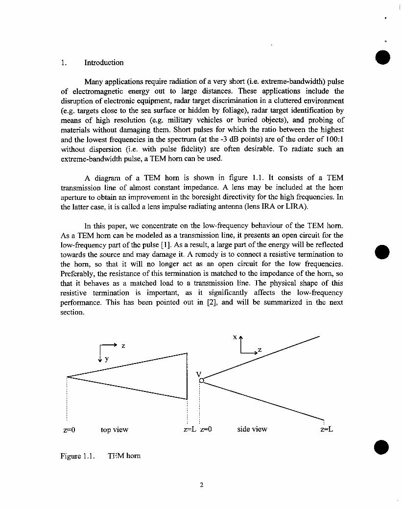
A diagram of a TEM horn is shown in figure 1.1. It consists of a TEMtransmission line of almost constant impedance. A lens may be included at the hornaperture to obtain an improvement in the boresight directivity for the high frequencies. Inthe latter case, it is called a lens impulse radiating antenna (lens IRA or LIRA).
In this paper, we concentrate on the low-frequency behaviour of the TEM horn.As a TEM horn can be modeled as a transmission line, it presents an open circuit for thelow-frequency part of the pulse [1]. As a result, a large part of the energy will be reflectedtowards the source and may damage it. A remedy is to connect a resistive termination to *the horn, so that it will no longer act as an open circuit for the low frequencies.Preferably, the resistance of this termination is matched to the impedance of the horn, sothat it behaves as a matched load to a transmission line. The physical shape of thisresistive termination is important, as it significantly affects the low-frequency
performance. This has been pointed out in [2], and will be summarized in the next
section.
x
r z
JY
,.=0 top view z=L z=O side view z=L
Figure 1.1. TEM horn

I
●
.
2. Design Considerations for the Low-Frequency Compensation
In the low-frequency limit, we are dealing with a quasistatic problem. Then,because of the voltage difference between the plates, there will be positive charge on theupper antenna plate and negative charge on the lower plate. As a consequence, theantenna (in combination with the terminating loop) has an electric dipole moment andthere is a toroidal electric-field distribution around it. Furthermore, the current that flowsthrough the antenna and the terminating loop gives the antenna (in combination with theloop) a magnetic dipole moment as well, and there is a magnetic field around the antenna,the properties of which are determined by the size and shape of the terminating loop andthe magnitude of the current. As was pointed out in [2,3], it is desirable to have themagnitudes and directions of both dipole moments matched in such a way that theycombine to orient the low-frequency radiation in the forward direction and cancel thelow-frequency radiation in the backward direction.
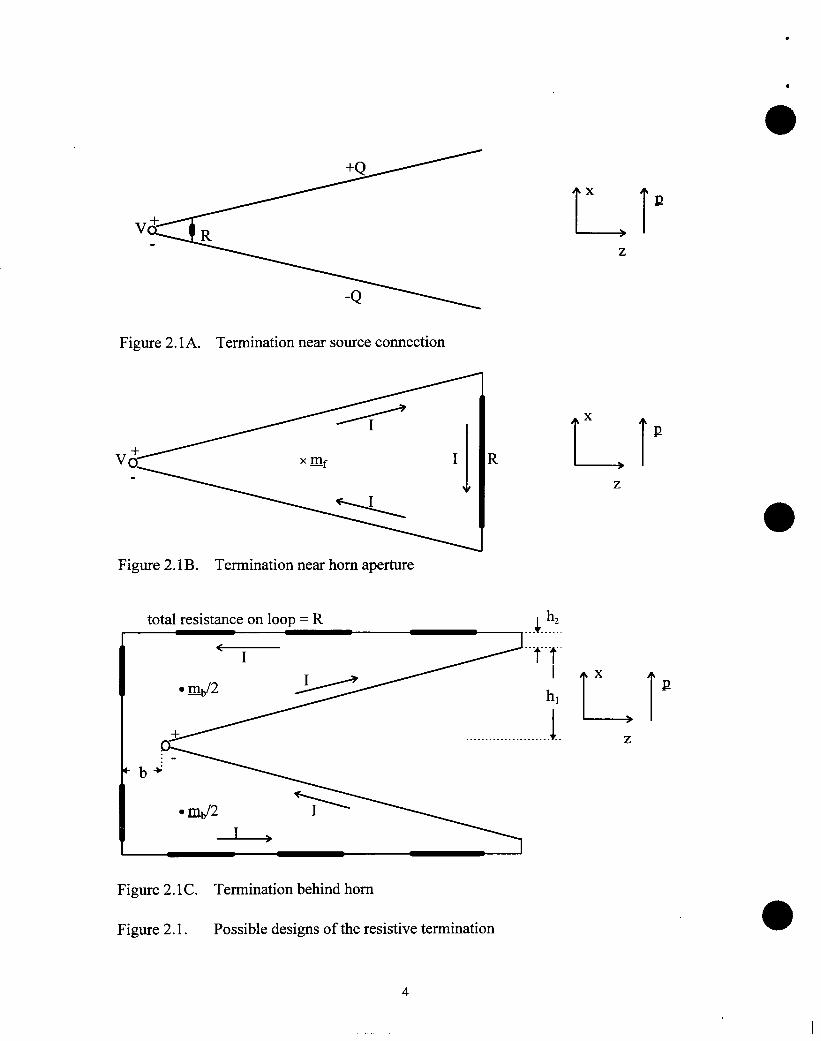
Consider the three possible designs in figure 2.1. If the resistor is placed near thesource, as in figure 2.1A, the electric dipole moment will dominate the magnetic one, andthe Iow-frequency antenna pattern will be toroidal. If the resistor is placed near the hornaperture, as in figure 2.1 B, the electric and magnetic dipole moments will, if theirmagnitudes are matched, combine in such a way that the Poynting vector, for lowfrequencies, is directed backward. This is of course just the opposite of what we want, asit is in the direction opposite to the high-frequency radiation. The design presented infigure 2.1 C reverses the orientation of the current loop, and hence in this case the electicand magnetic dipole moment will, if their magnitudes are matched, combine to direct thePoynting vector for low-frequencies forward. A cardioid antenna pattern will result forthese low frequencies, with a null in the backward direction.
With the design presented in figure 2.1 C compared to the design without acompensating loop, we can achieve the following:
1. avoidance of reflections back into the source,2. better directivity for low frequencies,3. a larger radiation bandwidth.
This will only be achieved when the magnitudes and directions of the electric andmagnetic dipole moment are matched. The matching condition, as explained in [2], is
mY= pXc ,mX= mz= O9 py= pz= 0, (2.1)
in which m,, mYand m=are the components of the magnetic dipole moment ~ in Am2, pX,pYand pZare the components of the electric dipole moment p in Cm, and c is the speed oflight in m/s. We will now discuss the parameters that may be varied to achieve thematching condition.
.
●
+Q
-Q
Figure 2.1A. Termination near source connection
L, Tx
P
z
z
Figure 2.1 B. Termination near horn aperture
total resistance on loop= R...+......T.T.
x
h, L, 1P
1........................ z
● r&/2T
Figure 2.lC. Termination behind horn
Figure 2.1. Possible designs of the resistive termination

*
,
m The electric dipole moment is determined by the charge distribution in the low-frequency limit, which in turn depends on the size and shape of the entire antenna-loopcombination and the voltage distribution on it. We assume that the voltage on the antennaplates as well as the size and shape of the plates are determined by other considerations inthe antenna design and cannot be varied freely anymore. The total resistance in the loophas to be equal to the characteristic impedance of the antenna, which also cannot bevaried freely anymore. Thus, what can still be varied to change p are the size and shape ofthe loop and the distribution of resistors along the loop. The magnetic dipole moment isdetermined by the magnitude of the current and the area of the loop. The magnitude ofthe current depends on the voltage and the resistance, which cannot be changed. Thus,what can still be varied to change m is the area of the loop. Combining the observationson the electric and magnetic dipole moment, we have to design the size and shape of theloop and the distribution of resistors along the loop in such a way that the matchingcondition is satisfied. Also, we want both moments to be large, in order to maximize theradiated power for low frequencies. The size of the loop should, however, not be muchlarger than the overall dimensions of the TEM horn, as in most applications the spaceavailable for the entire structure is limited.
Consider figure 2.1 C, in which, for a rectangular loop shape, some variables areintroduced.From this figure, we conclude that, to optimize our design, we can vary
- hz, the height above the aperture rim,- b, the distance behind the apex of the antenna,
the cross section of the loop, e.g. one or more wires, their radii, or strips withcertain widths,- the distribution of the resistors along the loop.
The parameter hz should always be kept small. In some applications, the availablespace for the antenna will hardly be larger than the antenna itself. The effect of increasingh2 is an increase in the area of the loop, which means an increase in the magnetic dipolemoment. The effect on the electric dipole moment can be positive as well as negative, butat a smaller rate.
The parameter b should not be large for the same reason as for hz, but as wealready had to reserve some space behind the antenna for the source, there will usually besome space available for the loop as well. The effect of an increase in b is an increase inthe area of the loop, which means an increase in the magnetic dipole moment. The effecton the electric dipole moment can be positive as well as negative, but at a smaller rate.
As loop cross sections, we have performed calculations on designs with one wireand with two parallel wires, in both cases with variable radii, as well as on strip-likestructures. We will present the results in Section 4. For a constant loop are% the variationof the loop cross section doesn’t affect the magnetic dipole moment. The way the electric
5

I
i.
dipole moment is afYected depends on how the total charge on the loop is affected. Theeffect can be both positive and negative. a
The distribution of resistors along the loop “doesn’t affect the magnetic dipole
moment. It does affect the charge distribution, and therefore electric dipole moment. In
general, when we move part of the resistors closer to the antenna aperture, pX decreases
significantly. When we move part of the resistors ftier away from tie aperture, PXincreases significantly.
In the next section, we will outline an analytical approach to obtain an antemadesign with the desired properties.

3. An Analytical Approach to Match the Electric and Magnetic Dipole Moments
In our analytical approach, we assume that the antenna and the compensatingloop, as depicted in figure 2.1 C, are both very long, so that end effects can be neglected.As a start, we take b=O, i.e. the loop doesn’t extend behind the source. The designprocedure then consists of the following steps:
1. Specifi the distribution of resistors along the loop and specifi hz.2. Knowing the distribution of resistors, solve for the voltage distribution alongthe loop. The voltage on the upper antenna plate is VO, the voltage on the lowerantenna plate is -Vo.3. Solve for the charge distribution on the entire structure (antenna plates andloop).4. Knowing the charge distribution, calculate the electric dipole moment p.5. Knowing the current and the loop shape, calculate m and compare m to pc (cf.(2. l)). If a modification is needed, go back to step 1 and repeat the procedure.
Obviously, the main challenge is in step 3. An efficient method to obtain thecharge distribution on a cylindrical structure (a two-dimensional problem) is given in[4,5]. Now, consider the cross section of our antenna+loop structure as given in figure
●3.1. The cross section has been taken at an arbitrary location between source and aperture(i.e. arbitrary z-coordinate). In this figure, W is the width of the plates at the apertureplane, and L is the distance between apex and aperture plane (cf. fig. 1.1).
..................................................
a. . . . . . . . . . . . . . . . . . . . . . . . .
I....... 0........................ P] 9 v]
2(h,’+h2) 2h1z.lL
~ -Po , -Vo
&w&>
J..................................0 -PI , -v]
Figure 3.1. Cross section of antenna+loop structure at arbitrary z
7

II IIUIIIII I I I -- I IIm mmm I III I II m-m II I ■I Mm m, IIMII., ■ ,, I .1,, m II --,1,. -,== I I I ■ ,=,,,=, mmI ,,-.,, . - mm- m m I m I n --mm m nm I . -mm-m
t,
4
Note that, as we have assumed the structure to be very long, we can, for each z, ●solve for the charge distribution as if the geometry were two-dimensional. We just needto obtain a relationship between the charge density distribution and the voltagedistribution for the two-dimensional case depicted in figure 3.1. The charge densitydistribution will be a function of z of course, as the distances between the conductors, thevoltages on the loop and the widths of the plates are all fi.mctions of z.
Because of symmetry, the problem reduces to the following equations:
pl = qlvl + %vo,po= C21V1+ %v(l ,
in which pl,0 denotes the charge per unit length on the
upper antenna plate, respectively, and V1,0 denotes theare functions of z. To obtain the coefficients c11, C12,
(3.1)
upper half of the loop or on thevoltages on these structures. AllC21,C22, we invoke the inverse
equations
VI = dllpl + d,2po ,V.= d21p1 + dzzpO .
Once matrix ~=(~,.) has
(3.2)
been found, matrix Q=(c.,m) can be obtained by taking the
inverse of Q. ‘To obtain the coefficients of ~, we use the relation between voltage andcharge dens~_tyin two dimensions [6]
(3.3)
in which 1Pdenotes the point of observation, I(1) denotes the point on the surface where
the surface charge density is given by p,(l), and 1 is a local coordinate on the surface (at
constant z) over which the integration is carried out.
Using (3.3) while making simplifying assumptions about the charge density
distribution p,(f) (for constant z) over the surface of each conductor, we establish linearrelations for each z between the charge densities pl and POand the voltages V 1 and Vo,
i.e. we have obtained the coefficients of matrix D. The coel%cients of C are obtained bytaking the inverse of D. The resulting relation between chwge densities and voltages is
2ZE (jPI(Z)= (ln(g)Vl(z)- ln(k(z))~o),
ln(j)ln(g) -ln2(k(z))(3.4a)

27t&(-JPo(z)= (lrl(f)vo - ln(k(z))v,(z)),
ln(~)ln(g) - ln2(k(z))
in which
(3.4b)
(3.4C)
In (3.4c), al is the radius of the wire, W is the width of the antenna plate at the aperture, his the height of the horizontal section of the wire above the apex of the antenna, L is thelength of the antenna, h, is half the vertical dimension of the aperture (at z=L). For theentire antenna+loop pXis subsequently calculated by means of (3.5):
L
J( ()2po zzhl
px =)
—+2pl(z)h G%.LZ=o
(3.5)
We have calculated an expression for p, for the case of a uniform distribution of resistorsalong the loop, i.e. a linear voltage distribution. Unfortunately, the integration in (3 .5)can, even in this simple case, not be carried out in closed form. We have split the integralin three separate integrals for small, intermediate and large z, made appropriateapproximations such that the three integrations could be carried out, and have added theresults.
WeW=50 cm,of resistors
will now give a numerical example. For VO=1.5 MV, Z=240 Cl, L= 137 cm,h1=50 cm, hz=l O cm, b=O, a1=2 cm, we obtain, with a uniform distributionalong the loop,
p,= 28 pCm, mY= 7.7 k&n2.
Hence, pX multiplied by the speed of light c is equal to 8.4 kAm2, which is 10’%0largerthan mY.As our goal is to match pXcand mY,this result indicates that just a small decreasein pXor a small increase in mYwill give us the desired result.
We can now proceed to adjust b, h2 or al and repeat the process, or we can derivean expression for pXresulting from another resistor distribution, and match pXc and mY.However, the approximations made to obtain this analytical result may be quite crude,especially the assumption of a very long structure and the assumptions concerning thecharge density distribution in the directions perpendicular to z. Therefore, we prefer toproceed with numerical calculations, in which the analytical result obtained thus far willserve as a usefi-d starting point and as a necessary check on the first numerical results.

r
4. A Numerical Approach to Match the Electric and Magnetic Dipole Moments
mAs pointed out by Barrington [7], the Method of Moments is very well suited to
calculate the charge distribution on an arbitrarily shaped three-dimensional perfectlyconducting structure, once the voltages are known everywhere on this structure. In threedimensions, the relation between the electrostatic potential V at the point of observationdenoted by IP and the surface charge density distribution P,(K) on a metal object is givenby [7]
(4.1)
On the antenna and the loop, the voltage distribution is known while the chargedensity distribution is to be calculated. To this aim, the structure is divided into many
planar quadrilateral panels. The wires in the structure are nonpkumr, but, as has been
proven by King [8], a wire of radius al can be modeled as a strip of width 4a1. Hence theentire structure can be divided into planar quadrilateral panels. On each panel, the voltage
and the charge density are supposed to be constant. The panels can always be made
sufficiently small to justifi this approximation. When we number the panels 1 to N, N
being the total number of panels, we have for the voltage on each panel the following
equation:N
Vn = ~LnmPS,m , (4.2)Mel
where, for combinations of panels that are not very close,
Lm= ‘“ , (4.3)47tEoRnm
in which Am is the area of panel m and ~~ is the distance between the centers of panels n
and m. The self term for m=n is given by [7]
For panels close together, special measures have to be taken, such as a further subdivisionof the panels. Finally, a matrix equation results:
(4.5)
where ~=wn), L=(Ln~), ~=(p,,~), in which p~ is unknown. The matrix equation is solvedby LU-decomposition.
As a check on the correctness of the software, we have applied the Method of
Moments to a very long TEM horn with compensating loop, as for this case the analytical ●
10

J
and numerical results should agree. Indeed, for a 10 meter antema+loop the results agreewithin 10°/0, which gives conildence in the correctness of the computer program. For the1.37 meter antenna+loop, the electric dipole moment, as calculated with the Method ofMoments (MoM), turns out to be about 30% larger than the analytical prediction.Apparently, the approximations made in the analytical approach are too crude indeed forsuch a not-very-long antenna. Therefore, in order to make the final design, we will relysolely on the numerical results, the correctness of which has been demonstrated for the 10meter antenna. For the 1.37 meter antenna+loop, the characteristic linear dimension of thepanels in the antenna and in the loop is 5 cm, with a maximum of 9 cm. The maximumlinear dimension of the panels in the ground pkme (to be introduced later) is 12 cm.Doubling the number of panels typically changes the calculated value for pX by 3%.
Note that the antenna, as depicted in figure 2.1 C, is symmetrical in the verticaldirection. Therefore, a ground plane (V=O) can be introduced and the lower part of theantenna+loop omitted. The subsequent calculations have been performed for anasymmetrical antenna with a finite ground plane (fig. 4.1), the reason being that theantenna will actually be built with a finite-sized ground plane. The size and shape of theground plane provide extra variables in the antenna design. In all cases, we choose itsminimum width to be 0.5 m at z=-O.25 m, and its maximum width to be 1.5 m. Theextension of the ground plane in the positive z-direction is kept as a variable. This mainlyinfluences pZ, which we assume to satis~ the condition pZ=Owhen its calculated absolutevalue is less than 0.2 ~Cm. All calculations with the finite-sized ground plane have beenperformed subject to the condition that the total charge on the entire structure be zero.
We start with the case where the compensating loop consists of one wire (figure4.1). The final design for this case, which has resulted after several numerical
experiments, has a uniform distribution of resistors along the entire wire (including thevertical sections). Further, h2=2.5 cm (this means the loop hardly takes more space in thevertical direction than the antenna itself), b= 15 cm (this means the loop extends 15 cmbehind the source, which is usually no problem), and al=l cm (this means the wire is notvery thin, which is good because it has to conduct currents of 12.5 kA, though in veryshort pulses). The ground plane extends to B 1.65 m. For this design, pX=l9 pCm andmY=5.7 kAm2, while the other components are zero. Hence, the matching condition (2.1)has been satisfied.
The sensitivity of the result to variation in some parameters is illustrated by the followingexamples:
When h2=5 cm instead of 2.5 cm, pXincreases by 3?40 while mYincreases by 8%.When b =22.5 cm instead of 20 cm, pXincreases by 1% while mYincreases by 3%.When a1=2 cm instead of 1 cm, pXincreases by 2’% while mYremains constant.When the resistors are distributed uniformly over the horizontal section of theloop only, while theremains constant.
vertical section is a bare wire, pXdecreases by 9 0/0while mY
11

v
When the ground plane extends to el .75 m instead of z=l .65 m, pZ=3 pCm whilep, decreases by 1%. m
We proceed with the case where the compensating loop consists of two wires
(figure 4.2). The reason for making a two-wire design is that these will have their
attachment points closer to the regions of maximm current density on the antenna plates,and are therefore expected to give a better pefiorrnance for part of the low-frequencyspectrum. In the final design for this case the wires are 25 cm apart, while again h2=2.5cm, al=l cm, and the resistors are uniformly distributed. The loop now extends 20 cm
behind the source (i.e. b=20 cm), and the ground plane extends to =1.60 m. For this
design, pX=20 pCm and mY=6.0 kAm2, while PY, P,, m., and m. me zero. Hence, thematching condition (2. 1) has again been satisfied.
top view
total resistance on loop= IU2
+
o ground plane
side view
Figure 4.1. TEM horn with one-wire compensating loop
12

J
top view
—
two parallel loops withtotal resistance R each
~o
side view
Figure 4.2. TEM horn with two-wire compensating loop
--------
-z:”----
----
top view
resistanceconcentratedat attachment point
2
+
o
side view
Fig. 4.3. TEM horn with one-triangle compensating loop
13

--------- W2----
u4”::::::------ --- ---- ---- Rf2
top view side view
Figure 4.4. TEM horn with two-triangle compensating loop
At this point, we have two designs for the low-frequency compensation of theTEM horn that are both easy to build and that both satsfy all requirements for the low
frequencies. For the intermediate and higher frequencies however, note that the fields o
associated with the charges in the loop and on the plate side facing the loop will radiate inunwanted directions. It is desirable to have a loop design that suppresses the radiation ofthe TEM fields above the TEM horn. This observation leads us to the design depicted infigure 4.3. We call it the TEM horn with the one-triangle compensating loop.
The idea behind this design is as follows. Fields propagating forward in the space
between the antenna plate and the loop will in this design be propagating in a structurethat looks like a receiving TEA4 horn with a ground plane. With a matched load at the end
(i.e. at the attachment point), their energy will be dissipated in the resistor. A 120 Clresistor is a matched load for this case, which is exactly the total resistance required in the
loop. Hence, in this case there are no fi.u-ther resistors along the loop; all resistance is
concentrated in the attachment point. The voltage along the loop is zero.
With b=20 cm and hz=2.5 cm, as before, we obtain pX=9.5 pCm, hence pXc=2.8kAm2. Again, mY=6.0 kAm2, as neither the current nor the area of the loop has changed.Hence we are far fi-om satisfying the matching condition pXc=mY.The reason is that by
bringing all resistance as far forward as possible, we are allowing a significant negativecharge on the loop, resulting in a low electric dipole moment. We cannot avoid this bymoving the resistors, as all resistance has to be concentrated in the attachment point inorder to act as a matched load. Making the loop narrower a the back, so that it’s negative Q
14

contribution to the electric dipole moment diminishes, will not help. In the limit of a verynarrow loop, we end up with a wire with all resistance concentrated at the attachmentpoint. From the one-wire design we know that this will still have a far too small electricdipole moment. Hence, we cannot use the one-triangle design.
An alternative design, in which the idea of the matched load can be used as well,is depicted in figure 4.4. Now there are two attachment points on the antenna plate. Wecall this the TEM horn with the two-triangle compensating loop. Note that radiationtraveling in the space between an antenna plate and the loop will still encounter, in thefrontal section, a structure that looks like a receiving TEM horn with a ground plane. Ineach attachment point, the matched load is provided by a 120 Cl resistor. An importantdifference with the previous design is that we now have some resistance left to placealong the loop at will! Two parallel 120 Cl resistors form together a 60 Q resistor, and wehave another 60 C?left to place along the loop. We can use this freedom to satisfi thematching condition. It turns out that this is achieved with b=l Ocm, h2=2.5 cm, and withthe 60 Cl placed at the point where where the loop makes an angle (as indicated in thefigure). Further, the ground plane extends to z=l .75 m. In this design, p,= 18 pCm andmY= 5.4 kAm2.
15

h’
5. Conclusion
We have presented several designs for a low-frequency compensated TEM hornwhich does not reflect low-frequency radiation towards the source and which, for thelowest frequencies, does not radiate a toroidal pattern but a cardioid pattern in the forward
direction. The compensating loop can be achieved with one or two wires or withadequately shaped plates, with the appropriate distribution of resistors along it. The TEMhorn with the two-wire compensating loop is expected to have a better performance thanthe horn with the one-wire loop for a part of the low-frequency spectrum. The TEM horn
with the two-triangle compensating loop has all the virtues of the TEM horn with the
two-wire compensating loop, while it is expected to have a better directivity for theintermediate and higher frequencies. Therefore, we have chosen this design to be
fabricated and tested. Its properties for the entire frequency spectrum will the subject offurther research, both experimental and computational.
Acknowledgement
The author wishes to thank the TNO Physics and Electronics Laboratory for giving him
the opportunity to conduct this research at the Phillips Laboratory, Dr. C.E. Baum(Phillips Laboratory) for valuable discussions, and Lt.Col. Dr. D.T. McGrath (PhillipsLaboratory) for providing most of the software. m
16

r1
t
e References
[1] E.G. Farr and C.E. Baurn, “A Simple Model of Small-Angle TEM Horns”, Sensorand Simulation Note 340, May 1992.
[2] C.E. Baum, “Low-Frequency Compensated TEM Horn”, Sensor and SimulationNote 377, January 1995.
[3] C.E. Baum, “Some Characteristics of Electric and Magnetic Dipole Antennas forRadiating Transient Pulses”, Sensor and Simulation Note 125, January 1971.
[4] J.C. Clements, C.R. Paul and A.T. Adams, “Computation of the CapacitanceMatrix for Systems of Dielectric-Coated Cylindrical Conductors”, IEEE Trans.Electromagnetic Compatibility, vol. 17, no.4, pp. 238-248, November 1975.
[5] C.R. Paul and A.E. Feather, “Computation of the Transmission-Line Inductanceand Capacitance Matrices from the Generalized Capacitance Matrices”, IEEE Trans.Electromagnetic Compatibility, vol. 18, no. 4, pp. 175-183, November 1976.
●[6] W.R. Smythe, Static and @wamic Electricity, Third Edition, Chapter 4,Hemisphere Publishing Corporation (Taylor and Francis Group), ISBN 0-89116-917-2,1989.
[7] R.F. Barrington, Field Computation by Moment Methods, First Printing, Chapter2, Macmillan Company, LCCCN 68-10184, 1968.
[8] R. W.P. King, The Theory of Linear Antennas, Chapter I-7, Harvard UniversityPress, LCCCN 56-5354, 1956.
17