I - Introduction © Copyright 2004, Gaetano Borriello and Randy H. Katz 1 Why study logic design?...
32
I - Introduction © Copyright 2004, Gaetano Borriello and R andy H. Katz 1 Why study logic design? Obvious reasons this course is part of the EE/CS/CE requirements it is the implementation basis for all modern computing devices building large things from small components provide a model of how a computer works More important reasons the inherent parallelism in hardware is often our first exposure to parallel computation it offers an interesting counterpoint to software design and is therefore useful in furthering our understanding of computation
-
Upload
myles-robinson -
Category
Documents
-
view
221 -
download
2
Transcript of I - Introduction © Copyright 2004, Gaetano Borriello and Randy H. Katz 1 Why study logic design?...

I - Introduction © Copyright 2004, Gaetano Borriello and Randy H. Katz
1
Why study logic design?
Obvious reasons this course is part of the EE/CS/CE requirements it is the implementation basis for all modern computing devices
building large things from small components provide a model of how a computer works
More important reasons the inherent parallelism in hardware is often our first exposure to
parallel computation it offers an interesting counterpoint to software design and is
therefore useful in furthering our understanding of computation

I - Introduction © Copyright 2004, Gaetano Borriello and Randy H. Katz
2
What will we learn in this class?
The language of logic design Boolean algebra, logic minimization, state, timing, CAD tools
The concept of state in digital systems analogous to variables and program counters in software systems
How to specify/simulate/compile/realize our designs hardware description languages tools to simulate the workings of our designs logic compilers to synthesize the hardware blocks of our designs mapping onto programmable hardware
Contrast with software design sequential and parallel implementations specify algorithm as well as computing/storage resources it will use
I - Introduction © Copyright 2004, Gaetano Borriello and Randy H. Katz
3
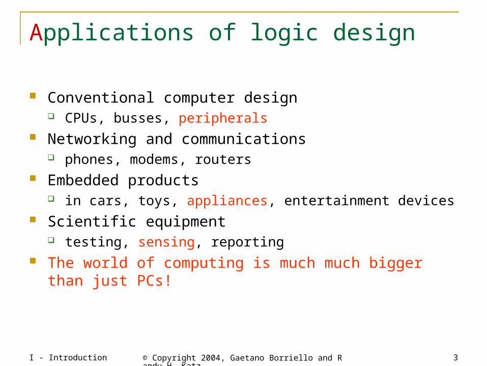
Applications of logic design
Conventional computer design CPUs, busses, peripherals
Networking and communications phones, modems, routers
Embedded products in cars, toys, appliances, entertainment devices
Scientific equipment testing, sensing, reporting
The world of computing is much much bigger than just PCs!
I - Introduction © Copyright 2004, Gaetano Borriello and Randy H. Katz
4
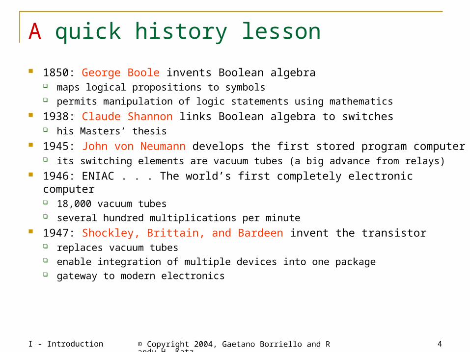
A quick history lesson
1850: George Boole invents Boolean algebra maps logical propositions to symbols permits manipulation of logic statements using mathematics
1938: Claude Shannon links Boolean algebra to switches his Masters’ thesis
1945: John von Neumann develops the first stored program computer its switching elements are vacuum tubes (a big advance from relays)
1946: ENIAC . . . The world’s first completely electronic computer 18,000 vacuum tubes several hundred multiplications per minute
1947: Shockley, Brittain, and Bardeen invent the transistor replaces vacuum tubes enable integration of multiple devices into one package gateway to modern electronics
I - Introduction © Copyright 2004, Gaetano Borriello and Randy H. Katz
5
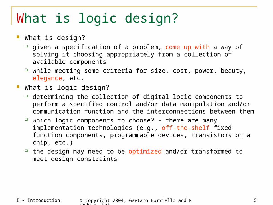
What is logic design? What is design?
given a specification of a problem, come up with a way of solving it choosing appropriately from a collection of available components
while meeting some criteria for size, cost, power, beauty, elegance, etc.
What is logic design? determining the collection of digital logic components to perform a
specified control and/or data manipulation and/or communication function and the interconnections between them
which logic components to choose? – there are many implementation technologies (e.g., off-the-shelf fixed-function components, programmable devices, transistors on a chip, etc.)
the design may need to be optimized and/or transformed to meet design constraints
I - Introduction © Copyright 2004, Gaetano Borriello and Randy H. Katz
6
sense
sense
driveAND
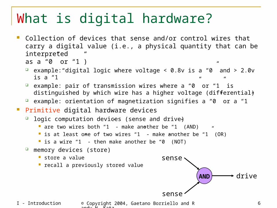
What is digital hardware? Collection of devices that sense and/or control wires that carry a
digital value (i.e., a physical quantity that can be interpreted as a “0” or “1”) example: digital logic where voltage < 0.8v is a “0” and > 2.0v is a “1” example: pair of transmission wires where a “0” or “1” is distinguished by
which wire has a higher voltage (differential) example: orientation of magnetization signifies a “0” or a “1”
Primitive digital hardware devices logic computation devices (sense and drive)
are two wires both “1” - make another be “1” (AND) is at least one of two wires “1” - make another be “1” (OR) is a wire “1” - then make another be “0” (NOT)
memory devices (store) store a value recall a previously stored value
I - Introduction © Copyright 2004, Gaetano Borriello and Randy H. Katz
7
What is happening now in digital design? Important trends in how industry does hardware design
larger and larger designs shorter and shorter time to market cheaper and cheaper products
Scale pervasive use of computer-aided design tools over hand methods multiple levels of design representation
Time emphasis on abstract design representations programmable rather than fixed function components automatic synthesis techniques importance of sound design methodologies
Cost higher levels of integration use of simulation to debug designs simulate and verify before you build
I - Introduction © Copyright 2004, Gaetano Borriello and Randy H. Katz
8
New ability: to accomplish the logic design task with the aid of computer-aideddesign tools and map a problem description into an implementation withprogrammable logic devices after validation via simulation and understandingof the advantages/disadvantages as compared to a software implementation
You must learn: concepts/skills/abilities Understanding the basics of logic design (concepts) Understanding sound design methodologies (concepts) Modern specification methods (concepts) Familiarity with a full set of CAD tools (skills) Realize digital designs in an implementation technology (skills) Appreciation for the differences and similarities (abilities)
in hardware and software design
I - Introduction © Copyright 2004, Gaetano Borriello and Randy H. Katz
9
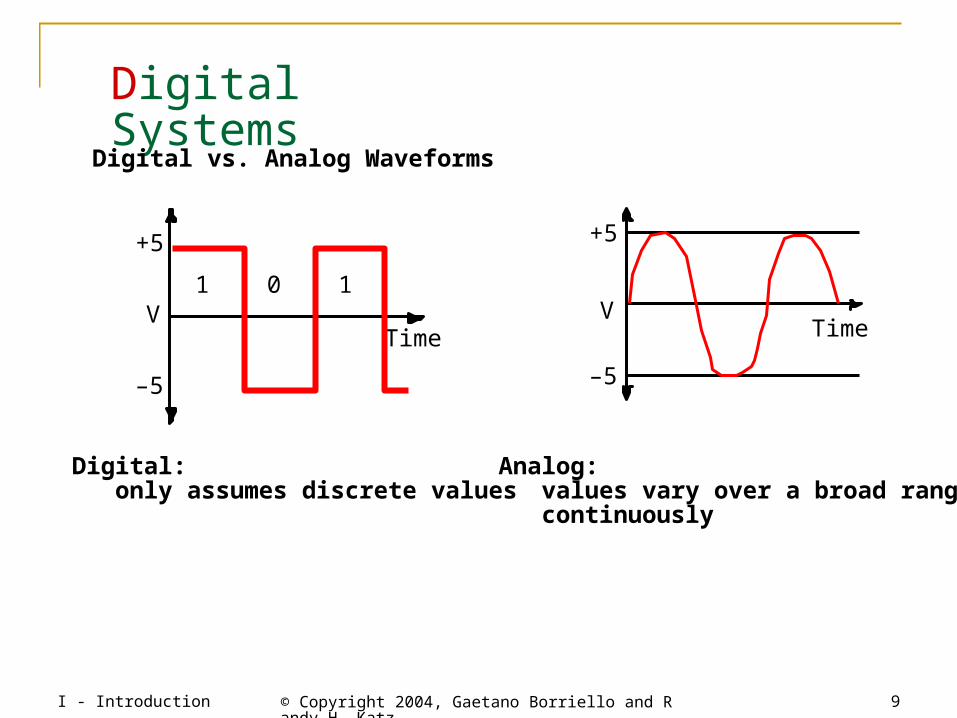
Digital Systems
Digital vs. Analog Waveforms
Analog: values vary over a broad range continuously
Digital: only assumes discrete values
+5
V
–5
Time
+5
V
–5
1 0 1
Time
I - Introduction © Copyright 2004, Gaetano Borriello and Randy H. Katz
10
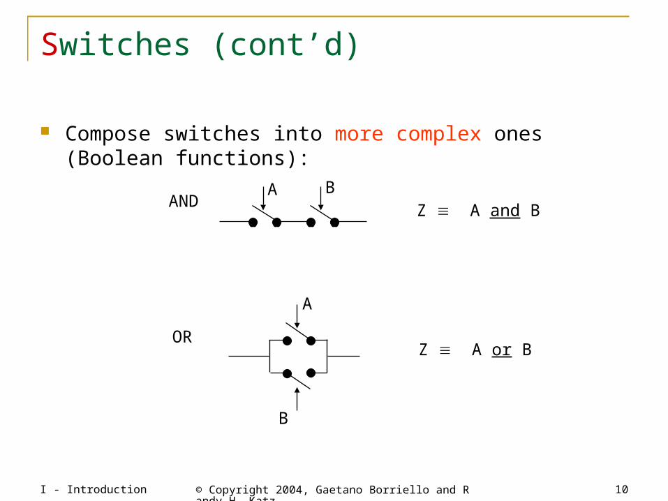
AND
OR
Z A and B
Z A or B
A B
A
B
Switches (cont’d)
Compose switches into more complex ones (Boolean functions):

I - Introduction © Copyright 2004, Gaetano Borriello and Randy H. Katz
11
conductingpath composed
of switchescloses circuit
current flowing through coil magnetizes core and causes normally closed (nc) contact to be pulled open
when no current flows, the spring of the contact returns it to its normal position
Relay networks
A simple way to convert between conducting paths and switch settings is to use (electro-mechanical) relays.
What is a relay?
What determines the switching speed of a relay network?
I - Introduction © Copyright 2004, Gaetano Borriello and Randy H. Katz
12
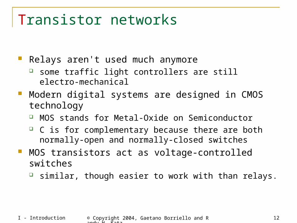
Transistor networks
Relays aren't used much anymore some traffic light controllers are still electro-mechanical
Modern digital systems are designed in CMOS technology MOS stands for Metal-Oxide on Semiconductor C is for complementary because there are both normally-open
and normally-closed switches MOS transistors act as voltage-controlled switches
similar, though easier to work with than relays.

I - Introduction © Copyright 2004, Gaetano Borriello and Randy H. Katz
13
n-channelopen when voltage at G is low
closes when:voltage(G) > voltage (S) +
p-channelclosed when voltage at G is low
opens when:voltage(G) < voltage (S) –
MOS transistors
MOS transistors have three terminals: drain, gate, and source they act as switches in the following way:
if the voltage on the gate terminal is (some amount) higher/lower than the source terminal then a conducting path will be established between the drain and source terminals
G
S D
G
S D

I - Introduction © Copyright 2004, Gaetano Borriello and Randy H. Katz
14
3v
X
Y 0 volts
x y
3 volts0v
what is the relationship
between x and y?
MOS networks
0 volts
3 volts
I - Introduction © Copyright 2004, Gaetano Borriello and Randy H. Katz
15
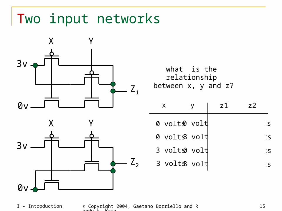
x y z1 z2
0 volts
3 volts
0 volts
3 volts
0 volts
0 volts
3 volts
3 volts
what is the relationship
between x, y and z?
Two input networks
3v
X Y
0v
Z1
3v
X Y
0v
Z2
3 volts
3 volts
3 volts
0 volts
3 volts
0 volts
0 volts
0 volts
NAND NOR
I - Introduction © Copyright 2004, Gaetano Borriello and Randy H. Katz
16
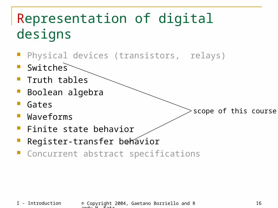
scope of this course
Representation of digital designs
Physical devices (transistors, relays) Switches Truth tables Boolean algebra Gates Waveforms Finite state behavior Register-transfer behavior Concurrent abstract specifications
I - Introduction © Copyright 2004, Gaetano Borriello and Randy H. Katz
17
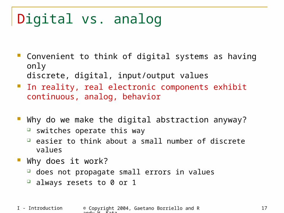
Digital vs. analog
Convenient to think of digital systems as having onlydiscrete, digital, input/output values
In reality, real electronic components exhibitcontinuous, analog, behavior
Why do we make the digital abstraction anyway? switches operate this way easier to think about a small number of discrete values
Why does it work? does not propagate small errors in values always resets to 0 or 1
I - Introduction © Copyright 2004, Gaetano Borriello and Randy H. Katz
18
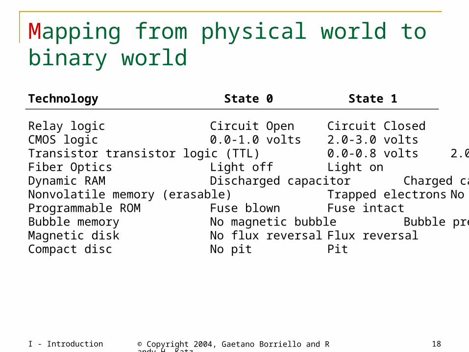
Technology State 0 State 1
Relay logic Circuit Open Circuit ClosedCMOS logic 0.0-1.0 volts 2.0-3.0 voltsTransistor transistor logic (TTL) 0.0-0.8 volts 2.0-5.0 voltsFiber Optics Light off Light onDynamic RAM Discharged capacitor Charged capacitorNonvolatile memory (erasable) Trapped electrons No trapped electronsProgrammable ROM Fuse blown Fuse intactBubble memory No magnetic bubble Bubble presentMagnetic disk No flux reversal Flux reversalCompact disc No pit Pit
Mapping from physical world to binary world

I - Introduction © Copyright 2004, Gaetano Borriello and Randy H. Katz
19
inputs outputssystem
Combinational vs. sequential digital circuits A simple model of a digital system is a unit with inputs and
outputs:
Combinational means "memory-less" a digital circuit is combinational if its output values
only depend on its input values
I - Introduction © Copyright 2004, Gaetano Borriello and Randy H. Katz
20
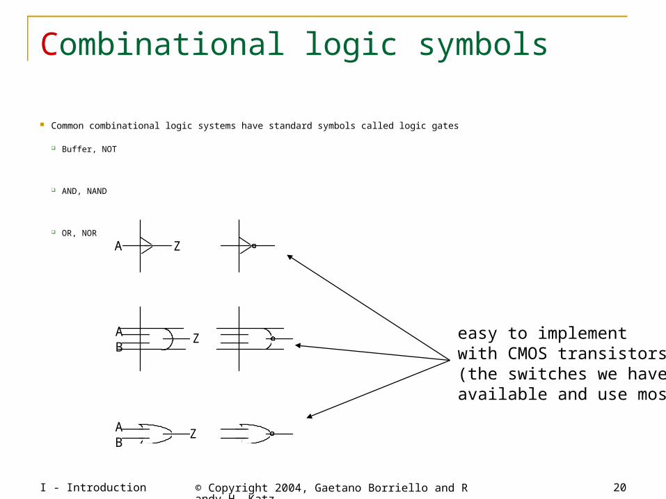
easy to implementwith CMOS transistors(the switches we haveavailable and use most)
Combinational logic symbols
Common combinational logic systems have standard symbols called logic gates
Buffer, NOT
AND, NAND
OR, NORZ
AB
Z
Z
A
AB
I - Introduction © Copyright 2004, Gaetano Borriello and Randy H. Katz
21
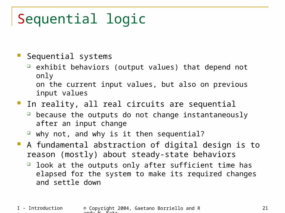
Sequential logic
Sequential systems exhibit behaviors (output values) that depend not only
on the current input values, but also on previous input values In reality, all real circuits are sequential
because the outputs do not change instantaneously after an input change
why not, and why is it then sequential? A fundamental abstraction of digital design is to reason
(mostly) about steady-state behaviors look at the outputs only after sufficient time has elapsed for the
system to make its required changes and settle down
I - Introduction © Copyright 2004, Gaetano Borriello and Randy H. Katz
22
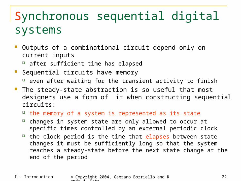
Synchronous sequential digital systems Outputs of a combinational circuit depend only on current inputs
after sufficient time has elapsed Sequential circuits have memory
even after waiting for the transient activity to finish The steady-state abstraction is so useful that most designers
use a form of it when constructing sequential circuits: the memory of a system is represented as its state changes in system state are only allowed to occur at specific times
controlled by an external periodic clock the clock period is the time that elapses between state changes it
must be sufficiently long so that the system reaches a steady-state before the next state change at the end of the period
I - Introduction © Copyright 2004, Gaetano Borriello and Randy H. Katz
23
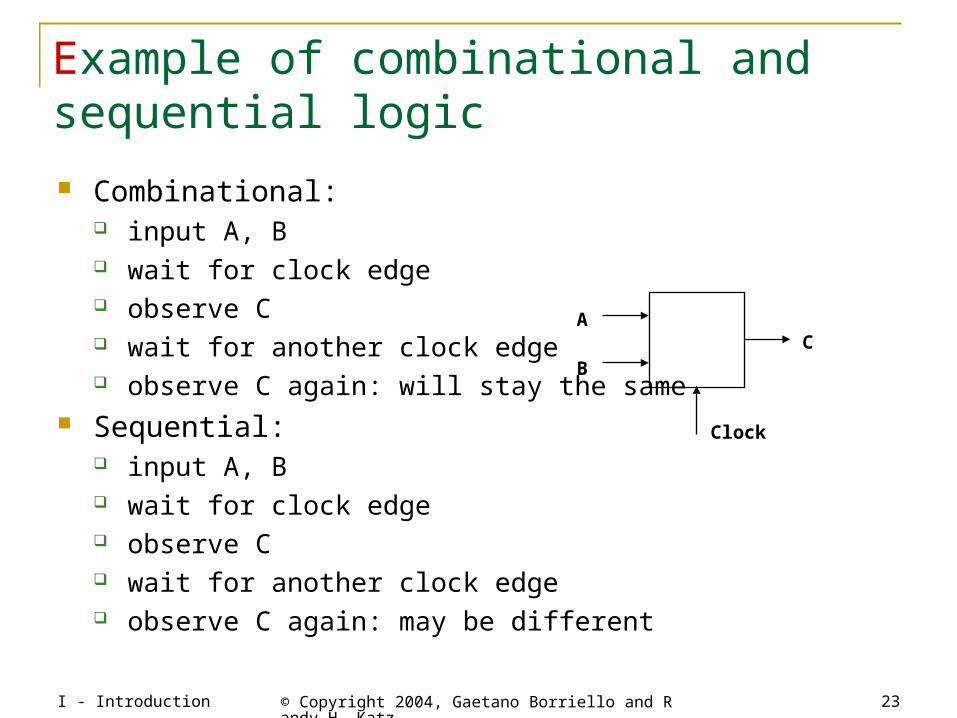
B
AC
Clock
Example of combinational and sequential logic
Combinational: input A, B wait for clock edge observe C wait for another clock edge observe C again: will stay the same
Sequential: input A, B wait for clock edge observe C wait for another clock edge observe C again: may be different

I - Introduction © Copyright 2004, Gaetano Borriello and Randy H. Katz
24
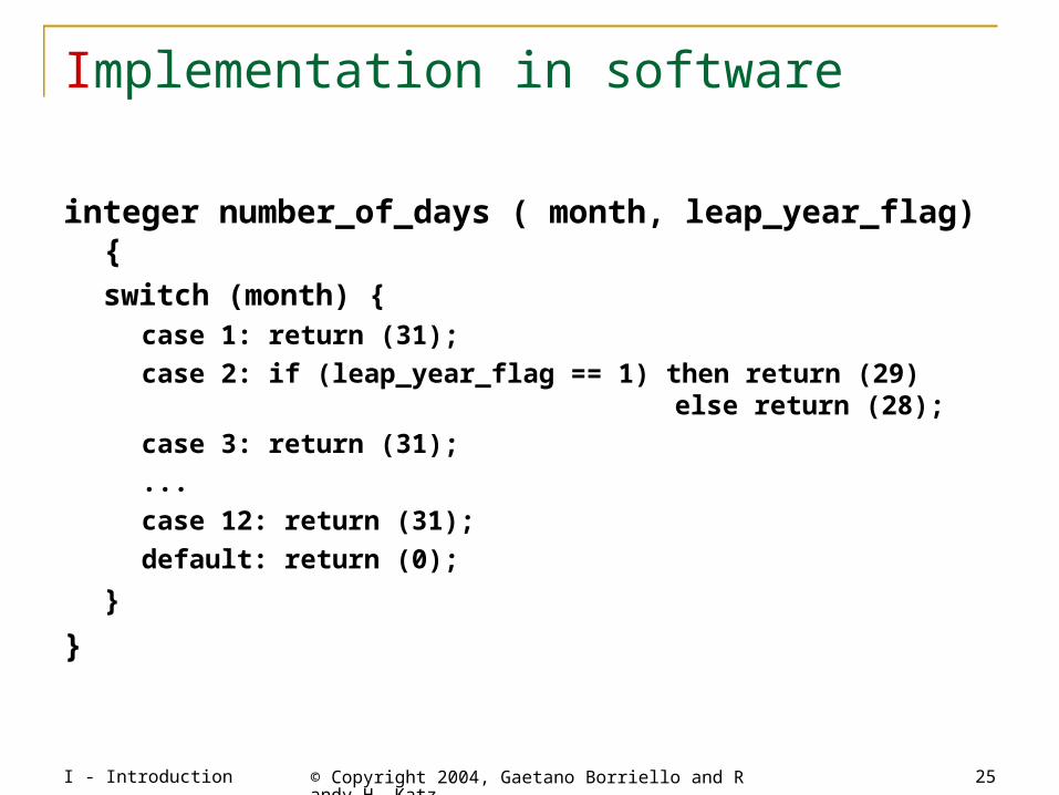
An example
Calendar subsystem: number of days in a month (to control watch display) used in controlling the display of a wrist-watch LCD screen
inputs: month, leap year flag outputs: number of days
I - Introduction © Copyright 2004, Gaetano Borriello and Randy H. Katz
25
Implementation in software
integer number_of_days ( month, leap_year_flag) {switch (month) {
case 1: return (31);
case 2: if (leap_year_flag == 1) then return (29) else return (28);
case 3: return (31);
...
case 12: return (31);
default: return (0);
}
}
I - Introduction © Copyright 2004, Gaetano Borriello and Randy H. Katz
26
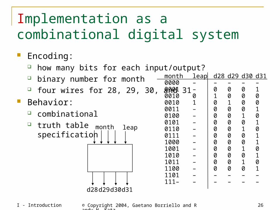
leapmonth
d28d29d30d31
month leap d28 d29 d30 d310000 – – – – – 0001 – 0 0 0 10010 0 1 0 0 00010 1 0 1 0 00011 – 0 0 0 10100 – 0 0 1 00101 – 0 0 0 10110 – 0 0 1 00111 – 0 0 0 11000 – 0 0 0 11001 – 0 0 1 01010 – 0 0 0 11011 – 0 0 1 01100 – 0 0 0 11101 – – – – –111– – – – – –
Implementation as acombinational digital system Encoding:
how many bits for each input/output? binary number for month four wires for 28, 29, 30, and 31
Behavior: combinational truth table
specification
I - Introduction © Copyright 2004, Gaetano Borriello and Randy H. Katz
27
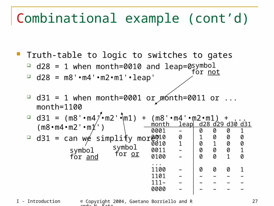
symbol for and
symbol for or
symbol for not
Combinational example (cont’d)
Truth-table to logic to switches to gates d28 = 1 when month=0010 and leap=0 d28 = m8'•m4'•m2•m1'•leap'
d31 = 1 when month=0001 or month=0011 or ... month=1100 d31 = (m8'•m4'•m2'•m1) + (m8'•m4'•m2•m1) + ...
(m8•m4•m2'•m1') d31 = can we simplify more?
month leap d28 d29 d30 d310001 – 0 0 0 10010 0 1 0 0 00010 1 0 1 0 00011 – 0 0 0 10100 – 0 0 1 0...1100 – 0 0 0 11101 – – – – –111– – – – – –0000 – – – – –
I - Introduction © Copyright 2004, Gaetano Borriello and Randy H. Katz
28
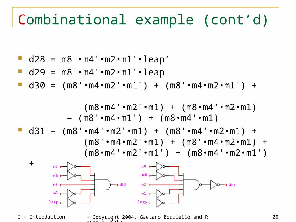
Combinational example (cont’d)
d28 = m8'•m4'•m2•m1'•leap’ d29 = m8'•m4'•m2•m1'•leap d30 = (m8'•m4•m2'•m1') + (m8'•m4•m2•m1') +
(m8•m4'•m2'•m1) + (m8•m4'•m2•m1) = (m8'•m4•m1') + (m8•m4'•m1)
d31 = (m8'•m4'•m2'•m1) + (m8'•m4'•m2•m1) + (m8'•m4•m2'•m1) + (m8'•m4•m2•m1) + (m8•m4'•m2'•m1') + (m8•m4'•m2•m1') + (m8•m4•m2'•m1')
I - Introduction © Copyright 2004, Gaetano Borriello and Randy H. Katz
29
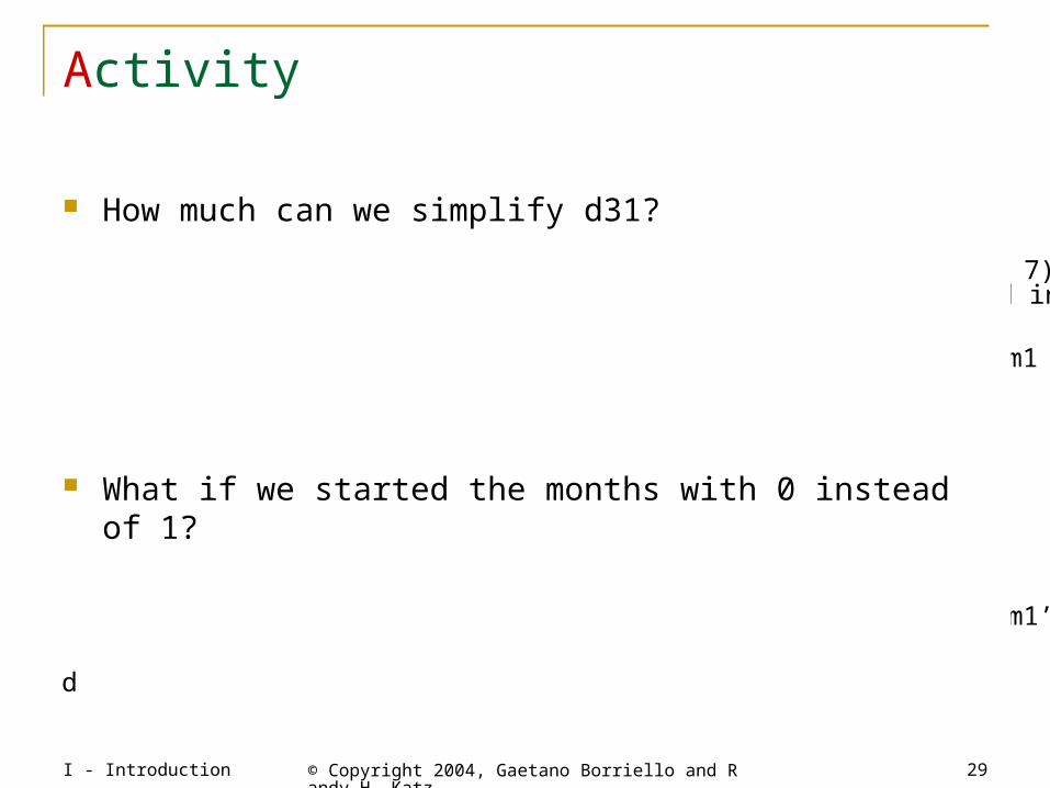
Activity
How much can we simplify d31?
What if we started the months with 0 instead of 1?(i.e., January is 0000 and December is 1011)
d31 is true if: month is 7 or less and odd (1, 3, 5, 7), ormonth is 8 or more and even (8, 10, 12, and includes 14)
d31 is true if: m8 is 0 and m1 is 1, or m8 is 1 and m1 is 0
d31 = m8’m1 + m8m1’
More complex expression (0, 2, 4, 6, 7, 9, 11):
d31 = m8’m4’m2’m1’ + m8’m4’m2m1’ + m8’m4m2’m1’ + m8’m4m2m1’+ m8’m4m2m1 + m8m4’m2’m1 + m8m4’m2m1
d31 = m8’m1’ + m8’m4m2 + m8m1 (includes 13 and 15)d31 = (d28 + d29 + d30)’

I - Introduction © Copyright 2004, Gaetano Borriello and Randy H. Katz
30
Combinational example (cont’d)
d28 = m8'•m4'•m2•m1'•leap’ d29 = m8'•m4'•m2•m1'•leap d30 = (m8'•m4•m2'•m1') + (m8'•m4•m2•m1') +
(m8•m4'•m2'•m1) + (m8•m4'•m2•m1) d31 = (m8'•m4'•m2'•m1) + (m8'•m4'•m2•m1) +
(m8'•m4•m2'•m1) + (m8'•m4•m2•m1) + (m8•m4'•m2'•m4') + (m8•m4'•m2•m1') + (m8•m4•m2'•m1')

I - Introduction © Copyright 2004, Gaetano Borriello and Randy H. Katz
31
system
data-path control
stateregisters
combinationallogic
multiplexer comparatorcode
registers
register logic
switchingnetworks
Design hierarchy
I - Introduction © Copyright 2004, Gaetano Borriello and Randy H. Katz
32
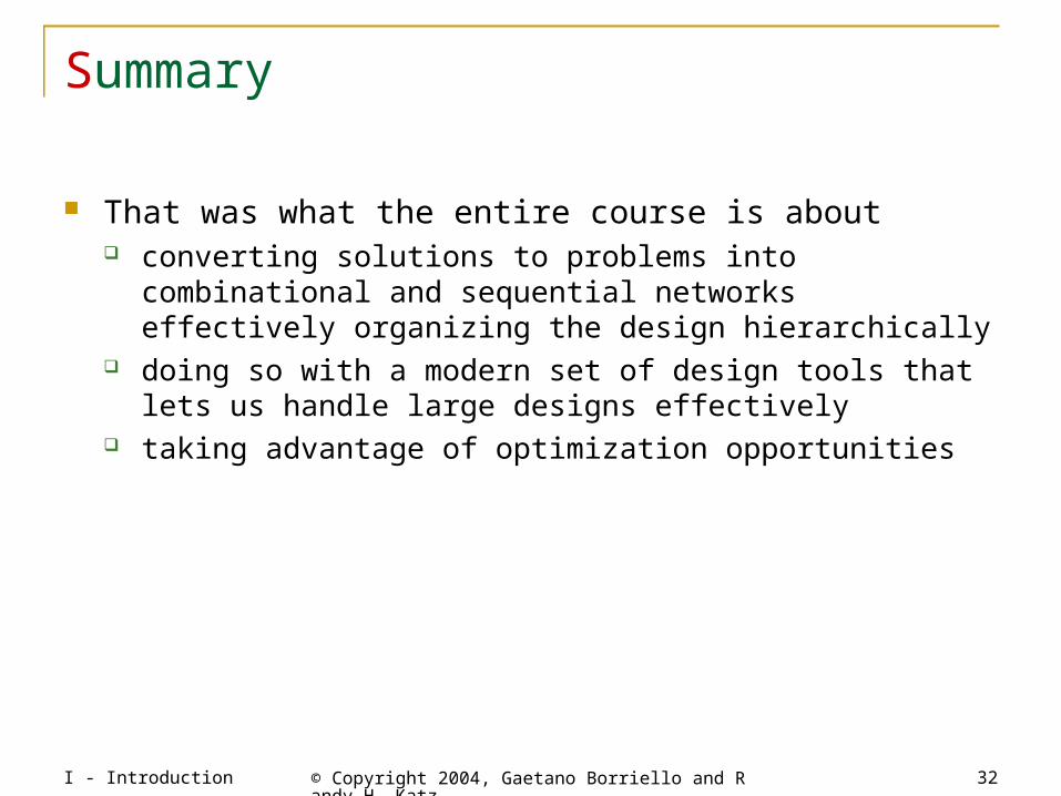
Summary
That was what the entire course is about converting solutions to problems into combinational and
sequential networks effectively organizing the design hierarchically
doing so with a modern set of design tools that lets us handle large designs effectively
taking advantage of optimization opportunities