
i EFFECT OF DIFFERENT COOLING RATE ON INTEGRATED …umpir.ump.edu.my/8391/1/CD8031_@_56.pdf ·...
24
i EFFECT OF DIFFERENT COOLING RATE ON INTEGRATED CIRCUIT(IC) PACKAGE AMIR SYAHMI NORDIN Thesis submitted in partial fulfillment of the requirements for the award of Bachelor of Mechanical Engineering with Automotive Engineering Faculty of Mechanical Engineering UNIVERSITI MALAYSIA PAHANG JUNE 2013
Transcript of i EFFECT OF DIFFERENT COOLING RATE ON INTEGRATED …umpir.ump.edu.my/8391/1/CD8031_@_56.pdf ·...

i
EFFECT OF DIFFERENT COOLING RATE ON INTEGRATED CIRCUIT(IC)PACKAGE
AMIR SYAHMI NORDIN
Thesis submitted in partial fulfillment of the requirements
for the award of
Bachelor of Mechanical Engineering with Automotive Engineering
Faculty of Mechanical Engineering
UNIVERSITI MALAYSIA PAHANG
JUNE 2013
vii
ABSTRACT
Currently, electronic products have shrunk into smaller size and in order toincrease the input/output (I/O) counts as well as to improve performance. Thegoal of this study is to determine the reliability and strength of the solder jointformed at the integrated circuit (IC) interconnection with the board. Thestrength of the joint is based on the intermetallic compound (IMC) formation atthe joint. Free lead based solders have been used nowadays due to theenvironmental and health hazard effect of the lead based solder. Two types ofsurface finish have been used in this study which was electroless/nickelimmersion gold (ENIG) and bare copper substrate as the reference in theresearch. All specimens will be subjected to reflow soldering with slow andfast cooling rate apply on the sample. Then, all specimens will undergoisothermal ageing at 150°C for 250 hour and 500 hour. The IMC formed at thesolder joints of all specimens were studied in terms of thickness and coolingrate applied on it. Characterization on the specimen is done by the cross sectionof the joint to see the IMC formation on the solder joint. It can be concludedthat, the fast cooling rate forms large IMC compared to slow cooling ratewhich is much thinner than fast cooling rate. Besides that, it was found thatIMCs thicknesses are proportional with ageing durations. However, thickerIMC was found on the bare copper substrate joint compare to ENIG surfacejoint after ageing treatment, indicating higher growth rate of IMCs formed atthe bare cooper substrate.

viii
ABSTRAK
Pada masa kini, saiz produk elektronik menjadi semakin kecil dan peningkatanmasukan/keluaran (I/O) adalah fokus utama dalam meningkatkan prestasi produkelektonik. Matlamat kajian ini adalah untuk mengukur kebolehpercayaan dankekuatan penyambungan pateri yang terbentuk pada litar bersepadu (IC) antarasambungan dan papan litar. Kekuatan sendi adalah berdasarkan pembentukansebatian intermetallik (IMC) pada penyambungan tersebut. Pateri berasaskan bebasplumbum sebagai pilihan pada masa kini kerana pateri berasaskan plumbummemberi kesan buruk kepada alam sekitar dan kesihatan penguna. Dalam kajian ini,dua jenis permukaan papan litar telah digunapakai iaitu tanpa elektrik / nikelrendaman emas (ENIG) dan substrat tembaga sebagai rujukan dalam penyelidikan.Semua spesimen akan melalui pematerian reflow dan kemudian melalui penyejukandengan kadar perlahan dan cepat. Kemudian, semua sampel akan menjalani penuaanisoterma pada 150 ° C selama 250 jam dan 500 jam. IMC yang terhasil padapenyambungan pateri pada semua spesimen telah dikaji dari segi ketebalandisebabkan kadar penyejukan berbeza yang dikenakan pada sampel. Pencirian padaspesimen itu dilakukan oleh keratan rentas yang sama untuk melihat pembentukanIMC pada penyambungan pateri. Berdasarkan kajian, dapat disimpulkan bahawakadar penyejukan cepat membentuk IMC bersaiz besar dibandingkan dengan kadarpenyejukan perlahan yang lebih nipis daripada kadar penyejukan cepat. Selain itu, iatelah mendapati bahawa ketebalan IMC adalah berkadar dengan jangka masapenuaan. Walau bagaimanapun, lebih tebal IMC ditemui pada permukaan substrattembaga berbanding dengan permukaan ENIG selepas rawatan penuaan,menunjukkan kadar pertumbuhan yang lebih tinggi IMC pada substrat tembaga.

ix
TABLE OF CONTENTS
PAGE
TITLE i
EXAMINER’S DECLARATION ii
SUPERVISOR’S DECLARATION iii
STUDENT’S DECLARATION iv
DEDICATION v
ACKNOWLEDGEMENT vi
ABSTRACT vii
ABSTRAK viii
LIST OF TABLES xii
LIST OF FIGURES xiii
LIST OF SYMBOLS xv
LIST OF ABBREVIATIONS xvi
CHAPTER 1 INTRODUCTION
1.1 Introduction 1
1.2 Objectives of Research 2
1.3 Scopes 2
CHAPTER 2 LITERATURE REVIEW
2.1 Electronic Packaging 3
2.2 Chips level Interconnection 42.2.1 Wire Bonding 42.2.2 Tape Automated Bonding 62.2.3 Flip Chip Bonding 7
2.3 Soldering 10
2.3.1 Introduction 102.3.2 Materials 10
x
2.3.2.1 Base Metals 102.3.2.2 Flux 11
2.3.3 Type of solders 122.3.3.1 Lead based solder 122.3.3.2 Lead free solder 14
2.3.4 Solderability 152.3.5 Soldering Method 17
2.3.5.1 Wave Soldering 182.3.5.2 Reflow soldering 19
2.4 Intermetallic Compound 21
2.4.1 Type of Intermetallic formation 222.4.1.1 Copper-Tin Intermetallics 222.4.1.2 Nickel-Tin Intermetallic 24
2.5 Surface Finish 25
2.5.1Finished on Copper 262.5.1.1 Organic Solderability Preservatives (OSP) 262.5.1.2 Immersion Silver (IAg) 272.5.1.3 Immersion Tin (ISn) 272.5.1.3 Direct Immersion Gold (DIG) 28
2.5.2Nickel based surface finish 282.5.2.1Electroless Nickel Immersion Gold 282.5.2.2Elctroless Nickel Electroless Palladium 29
Immersion Gold2.5.2.3 Electroless Nickel Immersion Gold 29
Electroless Gold
CHAPTER 3 METHODOLGY
3.1 Introduction 31
3.2 Substrate 33
3.3 Surface Preparation for Copper Substrate 33
3.4 Electroless Nickel Plating 343.4.1 Experimental set-up for Electroless Nickel Plating 353.4.2 Immersion Gold Plating 36
3.5 Reflow Soldering 383.5.1 Solder Mask 383.5.2 Flux Application 383.5.3 Solder Ball Placement 393.5.4 Reflow 39
3.6 Cooling Rate 40

xi
3.7 Isothermal Ageing 41
3.8 Characterization 413.8.1 Characterization specimen at cross section 41
3.10 Specimen Identification 42
CHAPTER 4 RESULT AND DISCUSSION
4.1 IMC Thickness with Different Cooling Rate 434.1.1 IMC thickness with slow cooling rate 444.1.2 IMC thickness with fast cooling rate 45
4.2 Isothermal ageing treatment toward IMC thickness 47
CHAPTER 5 CONCLUSION AND RECOMMENDATION
5.1 Conclusion 51
5.2 Recommendation 52
REFERENCES 53
APPENDICE 56
A Philips HP8100 technical specifications catalog 56

xii
LIST OF TABLES
Table No. Titles Page
2.1 Interconnection in electronic system 4
2.2 The comparison of three wire bonding process 5
2.3 Comparison between interconnection 9
2.4 Mechanical properties of Tin at different wt (%) 12
2.5 Phases in reflow soldering 20
3.1 Electroless nickel plating bath chemical composition and 34Parameter details
3.2 Immersion gold plating bath chemical composition and 36parameter details
3.3 Chemical Composition in Klemm Solution II 40
3.4 List of specimen investigated 41
4.1 IMC thickness of all specimens 43
4.2 Cross section of different thickness for ENIG with 49fast cooling rate and slow cooling rate using SEM

xiii
LIST OF FIGURES
Figure No. Titles Page
2.1 Schematic representation of the geometry of a ball/wedge 6
2.2 TAB 7
2.3 Phase diagram of Tin-Lead 13
2.4 Solder on an oxide plate and a clean plate 15
2.5 Definition of contact angle and related surface tension 17
2.6 The effect of surface tension on wetting 17
2.7 Schematic showing wave soldering flow process 18
2.8 Typical reflow profile for eutectic solder 19
2.9 Intermetallic layer formed at the solder/base metal 21
2.10 Phase diagram of copper/tin (Cu/Sn) at room temperature 22
2.11 Intermetallic formation between copper and tin 23
2.12 Phase diagram of nickel/tin (Ni/Sn) 24
3.1 Experimental flowchart 31
3.2 Copper substrate with dimension 32
3.3 Pretreatment process steps for copper substrates prior to 33Electroless Nickel plating process
3.4 Schematic diagram of equipment set-up of 35electroless nickel (EN) plating
3.5 Schematic diagram of equipment set-up of 36immersion gold (IG) plating
3.6 Copper substrate after flux application and solder 38balls arrangement
3.7 Reflow temperature profile 39
4.1 Cross sectional of intermetallic formation on bare copper 44surface finish using for slow cooling rate
xiv
4.2 Cross sectional of intermetallic formation on ENIG surface finish 44for slow cooling rate using
4.3 Cross sectional of intermetallic formation on ENIG surface finish 45for fast cooling rate
4.4 Graph of different IMC thickness versus cooling rate 46
4.5 Graph of IMC thickness on bare copper versus Ageing duration 47
4.6 Graph of IMC thickness on ENIG versus ageing duration 47
4.7 Graph of IMC thickness versus Ageing duration 48

xv
LIST OF SYMBOLS
SymbolsA Heat transfer surface area
h Convections heat transfer coefficient
Q Heat TransferT Temperature of surfaceT Temperature of the fluid sufficiently far from the surface
xvi
LIST OF ABBREVIATIONS
Ag Silver
Au Gold
Cu Copper
DIG Direct Immersion Gold
EN Electroless Nickel
ENIG Electroless Nickel Immersion Gold
ENIGEG Electroless Nickel Immersion Gold Electroless Gold
ENEPIG Electroless Nickel Electroless Palladium Immersion Gold
H2SO4 Sulfuric Acid
IC Integrated Circuit
ILB Inner Lead Bonds
IG Immersion Gold
ImAg Immersion Silver
IMC Intermetallic Compound
I/O Input/Output
ISn Immersion Tin
KauCN2 Potassium Cynoaurate
NaOH Sodium Hydroxide
Ni Nickel
OLB Outer Lead Bonds
OSP Organic Solderability Preservatives
Pb Lead

xvii
RoHS Restriction of use of Hazardous Substances
SEM Scanning Electron Microscope
Sn Tin
TAB Tape Automated Bond

CHAPTER 1
INTRODUCTION
1.1.1 INTRODUCTION
Heart of electronic system control is integrated circuit (IC), and since they are
sensitive to electrical, mechanical, physical and chemical influences, they require
special considerations by the packaging industry. Today‘s demand on high
performance, high reliability and low cost of circuit and system level requirements
make the packaging industry to have better understanding of existing and emerging
IC packaging technologies. Before board mounting, the plastic package is exposed to
humidity.
Lead based solders have been widely used in the electronic industry for a
considerable time. Nowadays, free lead based have been used in industry due to the
environmental and health hazard issues, lead-based solders are being phased out
from the industry. Initiatives, both by governmental and non-governmental agencies
have been taken to gradually replace lead-based solders such as Sn-Pb solders with
lead-free solders such as Sn-Ag and Sn-Ag-Cu solders.
Reliability issues are usually related to the solder joint intermetallic
compounds. The IMC is formed between the solder and substrate surface finish and
functions to provide mechanical, thermal, and electrical connections through the

2
solder joint. During reflow soldering, due to the high temperature conditions, a
reaction usually occur between the solders and the surface finish layers which in turn
form layers of intermetellic compound at the interface of the solder joints. The
formation of solder joint requires intermetallic compounds. However, excessive
thickness of IMCs will embrittle the solder joint due to its hard and brittle properties.
The brittle property of IMCs caused the strong stress concentration effect during the
thermal cycles, and cracks were found to initiate and propagate near the IMC layers
(Jene et al., 2011). So, study and characterization on the IMCs formed are essential
in order to achieve a good and reliable solder joint.
1.1.2 OBJECTIVES
The objectives of this research are:
i. To determine the effect of various cooling rates on IMC formation using Ni-
Au/Cu coating
ii. To investigate the effect of ageing treatment on thickness of the IMCs formed
at the solder joints.
1.1.3 SCOPE
In this research, different cooling rates on the IC package are conducted.
Through these different cooling rates, the solder joint reliability will be tested. To
create the joint, formation of IMC is necessary at the joint. The characterization of
intermetallic formation at the interface, from the aspect of thickness composition is
observed. However, excessive growth of IMC may lead to degradation of solder joint
strength. Therefore, the formation of IMC needs to be controlled to produce strong
and reliable older joint. Thus, the work is focuses on effect of cooling rates to control
the IMC formation and grain size. Besides that, investigation of isothermal ageing
effect on intermetallic formation at the solder joint.
CHAPTER 2
LITERATURE REVIEW
2.1 ELECTRONIC PACKAGING
In the globalization era, electronic components or gadget play big parts in
advanced world. The advanced country in the world can be classified through their
advanced gadget. These advanced gadgets became high demand and made the
manufacturers continuous develop the electronic gadget to meet the market needs.
With increasing demand of electronic devices in every field, electronic packaging
is gaining more importance, particularly for high-density applications. To ensure the
optimum performance of an electronic device a good electronic device is essential.
Electronic packaging compiles five functions which are (Harper, 2000):
i. A structure to support and protect the chip
ii. Connections for providing electrical current that powers the circuits on the
chip
iii. Connections for signal lines leading onto and off the silicon chip
iv. A wiring structure for signal and power interconnections within a system and
for input/output I/O
v. A meant for removing the heat generated by circuits

4
2.2 CHIP LEVEL INTERCONNECTS
There are three main methods for the chip-to-carrier connection assemblies
which are widely deployed in the electronic industry. They are the chip and wire
(wire bonding), tape automated bonding (TAB) and flip chip attachment.
Table 2.1: Interconnections in Electric Systems
Interconnection level Characterization Interconnectiontechnology
Zero Level Intrachip interconnections Built up layers of metaland dielectric materials
First Level Chip to package Wire bonding, TapeAutomated Bond, FlipChip
Second Level Packaged chip to substrate Solder, sockets,conductive adhesives,printed circuit board
Third Level Board to board Sockets, edge cardcontacts
Source: Tummala (2001)
2.2.1 Wire bonding
In the ball-wedge wire bonding process, the gold wire is ball bonded to the
chip bond pad surface as shown, and wedge bonded to a substrate pads as shown in
Figure 2.1. Wire bonding materials used in a ball bonding process mainly include the
bonding wire and bonding tool. Axial symmetric ceramic tools with vertical feed
holes are called capillaries for ball bonding tools. (Harper, 2000).
In the bonding process, the ball is formed at the tip of the capillary and then
pressed against the chip. The pressure and the thermosonic action result in bonding
the ball to the chip. The wedge bond can then be placed anywhere on a 360° arc
around the ball bond, using the capillary tip (Harper, 2000). This is the main
advantage that makes this process attractive for high speed automated bonding where
the bonding head or package table does not have to rotate to form the wedge bond.
5
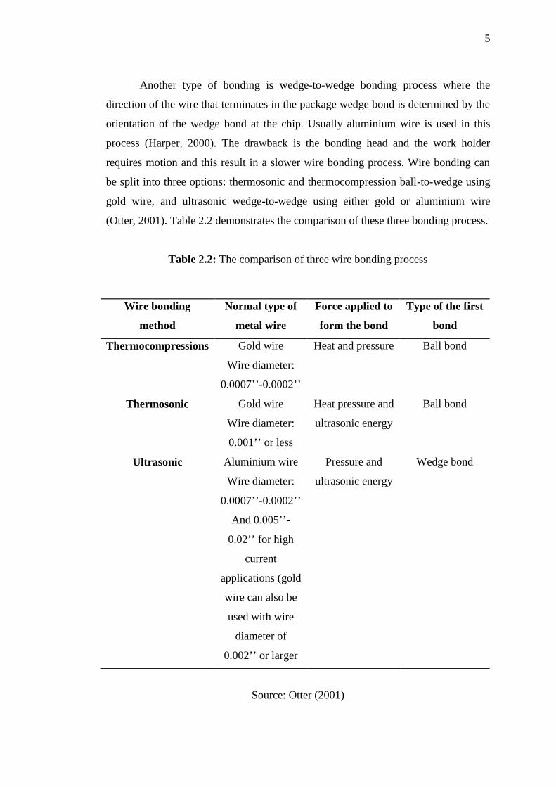
Another type of bonding is wedge-to-wedge bonding process where the
direction of the wire that terminates in the package wedge bond is determined by the
orientation of the wedge bond at the chip. Usually aluminium wire is used in this
process (Harper, 2000). The drawback is the bonding head and the work holder
requires motion and this result in a slower wire bonding process. Wire bonding can
be split into three options: thermosonic and thermocompression ball-to-wedge using
gold wire, and ultrasonic wedge-to-wedge using either gold or aluminium wire
(Otter, 2001). Table 2.2 demonstrates the comparison of these three bonding process.
Table 2.2: The comparison of three wire bonding process
Source: Otter (2001)
Wire bonding
method
Normal type of
metal wire
Force applied to
form the bond
Type of the first
bond
Thermocompressions Gold wire
Wire diameter:
0.0007’’-0.0002’’
Heat and pressure Ball bond
Thermosonic Gold wire
Wire diameter:
0.001’’ or less
Heat pressure and
ultrasonic energy
Ball bond
Ultrasonic Aluminium wire
Wire diameter:
0.0007’’-0.0002’’
And 0.005’’-
0.02’’ for high
current
applications (gold
wire can also be
used with wire
diameter of
0.002’’ or larger
Pressure and
ultrasonic energy
Wedge bond

6
Figure 2.1: Schematic representation of the geometry of a ball/wedge
Source: Otter (2001)
2.2.2 Tape Automated Bonding (TAB)
TAB is the process of mounting a polymer material die on a flexible tape,
such as polyimide. The mounting is done as the bonding sites of the die, usually in
the form of gold or solder of bumps or balls, are connected to fine conductors on
the tape, which offer the means that of connecting the die to the package or directly
to external circuits. Sometimes the tape bonded tape is already contains the actual
application circuit of the die (Siliconfareast, 2001).
The TAB bonds connecting the die and the tape are known as inner lead
bonds (ILB), while those that connect the tape to the package or to external circuits
are known as outer lead bonds (OLB). Single-sided tape usually used in TAB,
although two-metal tapes are also available. A commonly-used metal in tapes is
copper; it can be electrodeposited on the tape or attached to the adhesives tape.
Photolithography is used to see the metal image of the tape patterns onto the circuit.
7
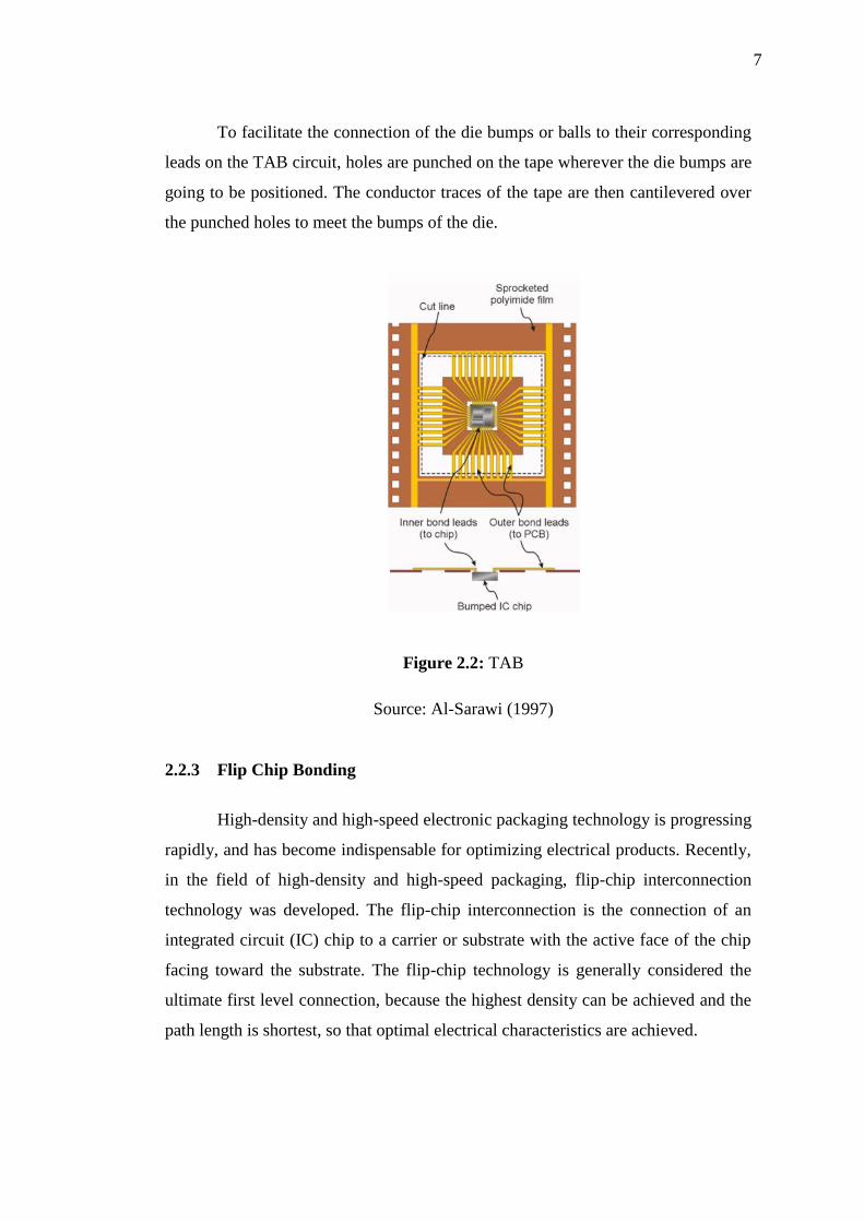
To facilitate the connection of the die bumps or balls to their corresponding
leads on the TAB circuit, holes are punched on the tape wherever the die bumps are
going to be positioned. The conductor traces of the tape are then cantilevered over
the punched holes to meet the bumps of the die.
Figure 2.2: TAB
Source: Al-Sarawi (1997)
2.2.3 Flip Chip Bonding
High-density and high-speed electronic packaging technology is progressing
rapidly, and has become indispensable for optimizing electrical products. Recently,
in the field of high-density and high-speed packaging, flip-chip interconnection
technology was developed. The flip-chip interconnection is the connection of an
integrated circuit (IC) chip to a carrier or substrate with the active face of the chip
facing toward the substrate. The flip-chip technology is generally considered the
ultimate first level connection, because the highest density can be achieved and the
path length is shortest, so that optimal electrical characteristics are achieved.
8
The term “flip-chip” refers to an electronic component or semiconductor
device that can be mounted directly onto a substrate, board, or carrier in a ‘face-
down’ manner. Electrical connection is achieved through conductive bumps built on
the surface of the chips. During mounting, the chip is flipped on the substrate, board,
or carrier, (hence the name ‘flip-chip’), with the bumps being exactly positioned on
their target locations. Because flip chips do not require wire bonds, their size is much
smaller than their conventional counterparts.
The flip-chip concept is not new; having been around as early as the 1960’s
when IBM used them for their mainframes. Since then, various companies have
developed the flip-chip to be utilized in thousands of various applications, taking
advantage of the dimension and cost benefits offered by this assembly technique.
Flip chips have likewise eliminated performance problems associated with
inductance and capacitance connected with bond wires.
In electronics the main intentions within the development of packaging is to
lower price, increase the packaging density, and improve the performance wheres
still maintaining or perhaps up improving the reliability of the circuits. Flip chip is a
process that facilitates direct attachment and electrical interconnection of the chip to
the substrate circuitry. Thus flip chip is as ideal concept of interconnection to fulfill
these visions as this kind of bonding requires only one level of connections between
the chip and the connection board. Table 2.2 will summarize the advantages and
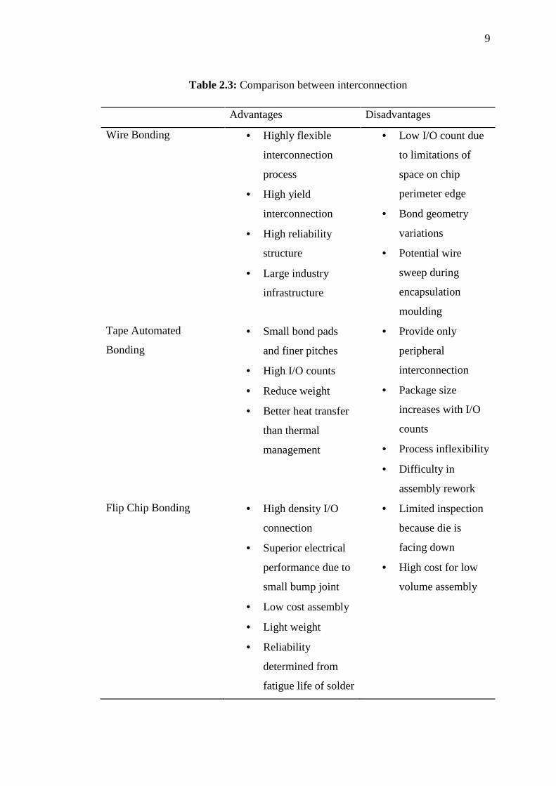
limitations of wire, tape automated and flip-chip bonding.
9
Table 2.3: Comparison between interconnection
Advantages Disadvantages
Wire Bonding Highly flexible
interconnection
process
High yield
interconnection
High reliability
structure
Large industry
infrastructure
Low I/O count due
to limitations of
space on chip
perimeter edge
Bond geometry
variations
Potential wire
sweep during
encapsulation
moulding
Tape Automated
Bonding
Small bond pads
and finer pitches
High I/O counts
Reduce weight
Better heat transfer
than thermal
management
Provide only
peripheral
interconnection
Package size
increases with I/O
counts
Process inflexibility
Difficulty in
assembly rework
Flip Chip Bonding High density I/O
connection
Superior electrical
performance due to
small bump joint
Low cost assembly
Light weight
Reliability
determined from
fatigue life of solder
Limited inspection
because die is
facing down
High cost for low
volume assembly

10
2.3 SOLDERING
2.3.1 Introduction
Nowadays, there are only two main classifications for soldering methods:
mechanical or non-electrical (using primarily acid flux) and electrical (using
primarily rosin flux). While advances in transistors, resistors, capacitors, diodes, and
particularly integrated circuits have revolutionized the world, these devices are of
very little value as individual components. As this component to be useful, they must
be electrically connected to each other and to mechanical devices. Majority of these
electrical connections are made by soldering. The solder does not only make
electrical connections, it also used to provide a physical connection between the
component and supporting printed circuit board. Throughout the years solder has
been used in various applications; however it was the invention of electronic devices
in the latter part of this century that led to rapid advances in soldering technologies.
The advances in electronics would not have resulted in today's mass production of
electronic equipment without accompanying advances in soldering technology.
2.3.2 Materials
Soldering is a method of making a permanent electrical and mechanical
connection between metals. Compare to glue which forms a solely physical adhesive
bond. Solder are chemically reacts with other metals to form a different alloy. While
there are various processes utilized in soldering, virtually all of them involve four
basic elements: base metals, flux, solder, and heat (Elenius, 1997).
2.3.2.1 Base Metals
Any metal that contacts the solder and forms an intermediate alloy are called
base metal. When attaching electronic components to a printed circuit board, the
component's leads or pins and board's metallic circuitry are the base metals which
will contact the solder. Many metals, such as copper, bronze, silver, brass, and a few
steels, without delay react with solder to create strong chemical and physical bonds.
11
Other metals, such as aluminium, high alloy steels, cast iron, and titanium, range
from vary from difficult to not possible to solder. The fact that there are metals that
don’t react with solder is important; these materials are used in the development of
soldering machinery. These metals can even be used as temporary covers for
components that do not seem to be soldered (Hoban and Lunt, 1997). Also of
importance to the electronic industry is the fact that ceramics do not react with
solder. The level of surface oxidation on the base metal and how solder will react
with it is a direct relationship between it. The more oxidation is present, the weaker
the solder bond. Most metals oxidize at a much accelerated rate when heated creates
a particular problem is the fact of soldering, since the chemical reactions associated
with soldering require high temperatures.
2.3.2.2 Flux
Flux is often applied as a liquid to the surface of the base metals prior to
soldering. Though flux really encompasses a range of functions, the primary and first
purpose of flux is to prevent the base metals from oxidizing while they are being
heated to the soldering temperature. The flux covers the surface to be soldered,
shielding it from oxygen and thereby preventing chemical reaction throughout
heating. Metal most fluxes also have and acidic component that is used to remove the
oxidation already present on the base. Applying a strong acid, it would be possible to
virtually completely clean off the oxidation layer. However, the use of strong acids
presents a heavy drawback. Oxidation layer is not limited to the oxidation layer the
corrosives of acids desirable to get rid of. Very strong acids can be damaging to
electronic components and a residue continues to corrode after the soldering process
is complete even the mild acids leave. There is a definite tradeoff between applying a
flux with a strong acid that removes a good deal of oxidation and applying a flux
with a mild acid that is not as corrosive. In any case, most fluxes in common use are
corrosive enough that their residue must be cleaned off after soldering.
When the liquid solder is applied, the flux must readily move out of the way
so the solder can come into direct contact with the base metal. During this method
some of the flux inevitably combines with the solder. Flux decorator typically take
12
advantage of this fact and style the flux to bring down the surface tension of the
solder upon contact, thereby permitting a more efficient wetting.
2.3.3 Type of Solder
2.3.3.1 Lead Based Solder
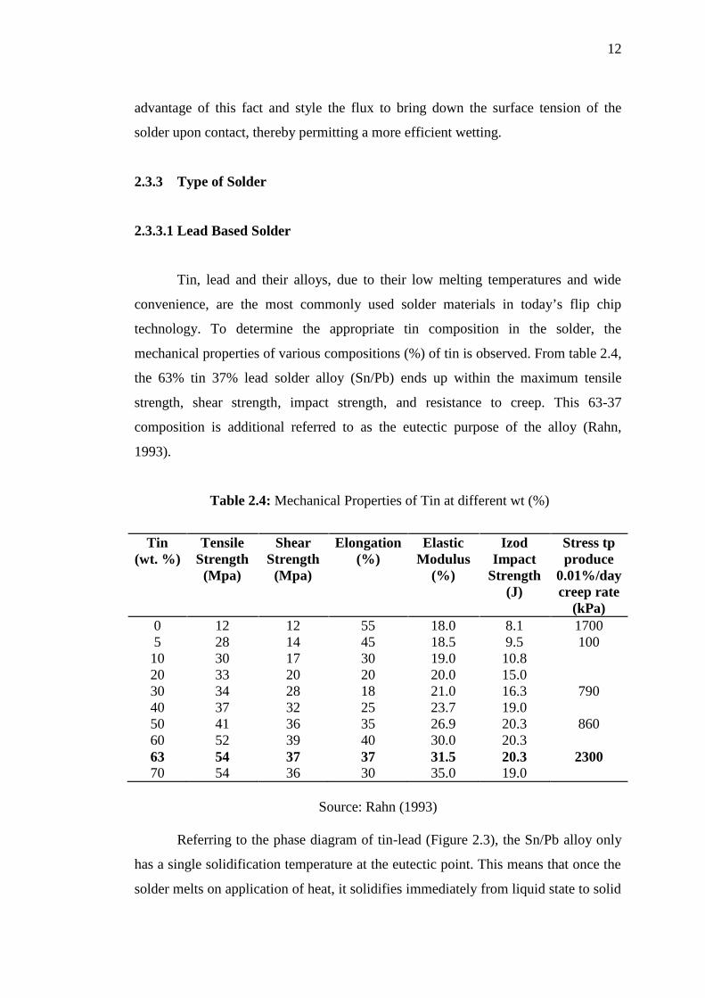
Tin, lead and their alloys, due to their low melting temperatures and wide
convenience, are the most commonly used solder materials in today’s flip chip
technology. To determine the appropriate tin composition in the solder, the
mechanical properties of various compositions (%) of tin is observed. From table 2.4,
the 63% tin 37% lead solder alloy (Sn/Pb) ends up within the maximum tensile
strength, shear strength, impact strength, and resistance to creep. This 63-37
composition is additional referred to as the eutectic purpose of the alloy (Rahn,
1993).
Table 2.4: Mechanical Properties of Tin at different wt (%)
Tin(wt. %)
TensileStrength
(Mpa)
ShearStrength
(Mpa)
Elongation(%)
ElasticModulus
(%)
IzodImpact
Strength(J)
Stress tpproduce
0.01%/daycreep rate
(kPa)0 12 12 55 18.0 8.1 17005 28 14 45 18.5 9.5 10010 30 17 30 19.0 10.820 33 20 20 20.0 15.030 34 28 18 21.0 16.3 79040 37 32 25 23.7 19.050 41 36 35 26.9 20.3 86060 52 39 40 30.0 20.363 54 37 37 31.5 20.3 230070 54 36 30 35.0 19.0
Source: Rahn (1993)
Referring to the phase diagram of tin-lead (Figure 2.3), the Sn/Pb alloy only
has a single solidification temperature at the eutectic point. This means that once the
solder melts on application of heat, it solidifies immediately from liquid state to solid


