I also provide a purpose-built ADC/DAC board to support ... 12 - Serial... · 5 The DAC used with...
14
1
Transcript of I also provide a purpose-built ADC/DAC board to support ... 12 - Serial... · 5 The DAC used with...

1

2

3
Ialsoprovideapurpose-builtADC/DACboardtosupportthelabexperiment.ThisanalogueI/OboardinonlyneededforPart3and4ofVERI.HoweverIwillnowbeexaminingthedigitalserialinterfacefortheseconverterchips.

4
ThisshowstheblockdiagramoftheanalogueI/OcardusedintheVERIexperiment.ItconsistsofaDAC(MCP4911)andaADC(MCP3002),bothusingSerialPeripheralInterface(SPI).TheDACoutputisbufferedbyaunitygainopampconnectedtotherightchannelofastereojacksocket.TheADChastwoinputchannels,onefromapotentiometerprovidingadcvoltage(CH0)andanotherfromthe3.5mmjacksocket(CH1).Finally,thereisa2nd orderlow-passactivefilter,theinputofwhichisdrivendirectlyfromadigitaloutputpinoftheCycloneFPGA.Thisisintendedtoprovidefilteringofapulse-widthmodulatedDACoutputfromtheFPGA.
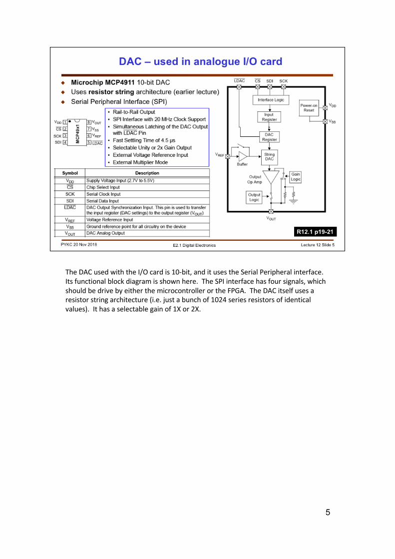
5
TheDACusedwiththeI/Ocardis10-bit,anditusestheSerialPeripheralinterface.Itsfunctionalblockdiagramisshownhere.TheSPIinterfacehasfoursignals,whichshouldbedrivebyeitherthemicrocontrollerortheFPGA.TheDACitselfusesaresistorstringarchitecture(i.e.justabunchof1024seriesresistorsofidenticalvalues).Ithasaselectablegainof1Xor2X.

6
TosendavaluetotheDACtooutput(i.e.producetheanalogueoutputVout),a16-bitvalueissenttotheDACchipinaserialmanner.TheChipSelect(SC)signalgoinglowindicatethatthisisthestartofthedata.Thisestablishesthebeginningofthedataframe.Firstdatabit(bit15)isalways0.Bit14determineswhetherthereferencevoltage(Vreg)isbufferedornotbuffered(viaaninternalopamp).Forourdesign,Vrefisaround3.3V.Bit13determinesthegainoftheDAC(x1orx2).Bit12issetto1ifyouareusingtheDAC,andsetto0ifyouwanttoshutdownthedevicetoconservepower.Bit11to2containsthe10-bitdataD[9:0]toconvertintoanaloguevoltageVout,MSBfirst.Bit1and0aredon’tcares.TheLDAC(lowactive)signalcanbeconnectedtogroundorusedalowactivestrobesignaltotransferthedatatotheDACregister(i.e.telltheDACtoupdateVout).IfLDACislow,DACupdatehappensonrisingedgeofCS_bar.

7
ThisisasimplifieddiagramshowinghowtheCycloneVFPGAisinterfacedtothetwodataconverters.TherearetwoADCchannelsandinourexperiment,wearemostlyusingchannel1viathe3.5mmjacksocket.Youwillbesupplyingspeechsignalsfromthedesktopcomputer.ThereisoneDACwhichdrivesboththesmallspeakerand,muchbetter,drivestheear-phone.(Pleasebringtheear-phonetothelab.)TheinterfacebetweentheFPGAchipandtheconvertersisthroughtheSPIbus.YouaregiventheVerilogdesignforthesetwointerfacemodules:spi2dac.vandspi2adc.v.Intherestofthislecture,Iwillbegoingthroughthedesignofthespi2dacmodule.

8
InordertousetheDAC,youhavetoincludetheinterfacemodule“spi2dac” inyourdesign.Thismodulehasaschematicshownabove.Ittakestwoinputs(inadditiontothe50MHzclocksignal):data[9:0]isthe10-bitdigitaldatatobeconvertedbytheDAC,andaloadsignalwhichisahighpulsetotriggerthespi2dacmoduletosendthe10-bitdatatotheDAC.
Theinternalworkingofsp2daccanbedividedinto4mainmodules.Thedivide-by-50moduleisstraightforward– itproducesa1MHzclockforthefinitestatemachine,andisgatedthroughtheANDgatetogeneratetheserialclocksignal(at1MHz).TheloaddetectormodulehandlestheloadcommandandproducescontrolsignalstotheSPIstatemachineandtheshiftregister.Theshiftregistersendsthecontrolbitsandthe10-bitdataseriallytotheSDIoutput.ThespicontrollerFSMisthemaincontrolmoduledesignedasastatemachine.
Wewillnowconsidereachsub-moduleindividually.

9
Thisisastraightforwardclockdivider.TheTerminalCount(TC)issetto24.Divideby50isdonebytogglingtheoutput(clk_1MHz)after25clockcycles.NotethatIgenerallyprefertouseadown-counterinsteadofanup-counter.Thecounter(ctr)issetto24,itthencountstozero.Outputistoggledandthecounter(ctr)isresettotheinitialvalueof24again.

10
WehaveTWOsignalstodetect:theloadpulseandthedac_cssignal.
StartingintheIDLEstate,whenloadsignalisasserted,westarttheDACcyclebyenteringtheWAIT_CSB_FALLstate.Inthisstate,dac_startisasserted,andwewaitforDAC_CStogolowfromtheSPIcontrollercircuit.Inthiscondition,theDACisinthemiddleofacceptinganewdataforconversion.WegotostateWAIT_CSB_HIGHTOwaitfortheconversiontobecompleted,whichisindicatedbyDAC_CSgoinghigh.Whenthathappens,wereturntotheIDLEstatewaitingforanother10-bitdatatobeloaded.

11
ThecontrollingFSMcontrollerisactuallysimplerthanitfirstappears.WeneedaFSMtohave18states.State0istheidlestate,waitingforanewdatatobesenttotheDAC.HereDAC_CS(whichislowactive)is‘1’ andwewaitforthedac_starttobeasserted.Thedefaultvalueofdac_csanddac_ldarespecifiedfirst.Bydefaultwealwaysgotothenextstate,i.e.statevaluegoesupby1.Oncethestatemachinemovestostate1,itjustgothroughtostate16,whichcorrespondstocycle0to15inthetimingdiagramhere.Attheendofstate16,wede-assertdac_cs(i.e.gohigh),assertdac_ld(low)andgobacktotheIDLEstate.
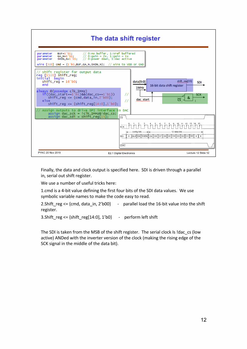
12
Finally,thedataandclockoutputisspecifiedhere.SDIisdriventhroughaparallelin,serialoutshiftregister.Weuseanumberofusefultrickshere:1.cmdisa4-bitvaluedefiningthefirstfourbitsoftheSDIdatavalues.Weusesymbolicvariablenamestomakethecodeeasytoread.2.Shift_reg<={cmd,data_in,2’b00}- parallelloadthe16-bitvalueintotheshiftregister.3.Shift_reg<={shift_reg[14:0],1’b0}- performleftshift
TheSDIistakenfromtheMSBoftheshiftregister.TheserialclockIs!dac_cs(lowactive)ANDedwiththeinverterversionoftheclock(makingtherisingedgeoftheSCKsignalinthemiddleofthedatabit).

13
IntheLabexperiment,youwilltestthespi2dac.vmodulebothwiththesimulatorandonthehardware(withascope)byinspectingtheoutputsignalsonthetestpins(locatedatthetopoftheI/Oboard).
Ex10and11aresimple,butwillgiveyouconfidencethattheinterfacemoduleworks.
14
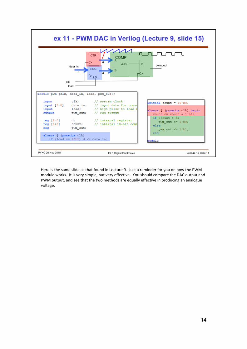
HereisthesameslideasthatfoundinLecture9.JustareminderforyouonhowthePWMmoduleworks.Itisverysimple,butveryeffective.YoushouldcomparetheDACoutputandPWMoutput,andseethatthetwomethodsareequallyeffectiveinproducingananaloguevoltage.