
Hybrid Solver and Measure Based Design - Molex CST MicroWave Studio, the...
21
DesignCon 2004 A Hybrid Measurement and Electromagnetic Field Solver Approach for the Design of High-Performance Interconnects: An Investigation of Traces and SMA Transitions Scott McMorrow Teraspeed Consulting Group LLC http://www.teraspeed.com [email protected] Alfred Neves TDA Systems http://www.tdasystems.com [email protected] DesignCon 2004 Copyright 2003, 2004 Hybrid Modeling Method 2 Teraspeed/TDA Systems
Transcript of Hybrid Solver and Measure Based Design - Molex CST MicroWave Studio, the...

DesignCon 2004 A Hybrid Measurement and Electromagnetic Field Solver Approach for the Design of High-Performance Interconnects: An Investigation of Traces and SMA Transitions Scott McMorrow Teraspeed Consulting Group LLC http://www.teraspeed.com [email protected] Alfred Neves TDA Systems http://www.tdasystems.com [email protected] DesignCon 2004 Copyright 2003, 2004 Hybrid Modeling Method 2 Teraspeed/TDA Systems

Abstract
As the cost of bringing complex high-performance systems to market increases and the time to market decreases, new methods must be used to insure first-pass design success. This paper describes a verifiable design method that establishes excellent signal integrity and enables leading-edge performance with common off-the-shelf materials. By integrating field solver and measurement-based modeling methods, the net process is verifiable. The optimum low-cost production design can be attained in the shortest time. This process yields unmatched time-domain and frequency-domain performance using off-the-shelf, generic, non-esoteric, low-cost materials.
Authors Biographies
Scott McMorrow, President, Teraspeed Consulting Group LLC Mr. McMorrow is an experienced technologist with over 20 years of broad background in complex system design, interconnect and Signal Integrity engineering, modeling and measurement methodology, engineering team building and professional training. Mr. McMorrow has a consistent history of delivering and managing technical consultation that enables clients to manufacture systems with state-of-the-art performance, enhanced design margins, lower cost and reduced risk. Mr. McMorrow is an expert in high-performance design and Signal Integrity engineering, and has been a consultant and trainer to engineering organizations worldwide. Mr. McMorrow can be reached at [email protected].
Albert Neves, Applications Engineer, TDA Systems Alfred P. Neves is an Applications Engineer for TDA Systems Inc. (www.tdasystems.com) and can be reached at [email protected].
Recent Publications: [1.] S. McMorrow, “Choosing the Right Connector,” Printed Circuit Design Magazine,
January 2003 [2.] S. McMorrow, “Handling Signal Return Current,” Printed Circuit Design Magazine,
September 2002 [3.] S. McMorrow, Rob Hinz, “Interconnect Engineering,” Printed Circuit Design
Magazine, March 2002 [4.] S. McMorrow, Rob Hinz, et al, “Attention to Details: The Transition From 2.5 to
10Gbps,” DesignCon 2002
DesignCon 2004 Copyright 2003, 2004 Hybrid Modeling Method 3 Teraspeed/TDA Systems

Introduction As the cost of bringing complex high-performance systems to market increases and the time to market decreases, new methods must be used to insure first pass design success. In the area of high-performance interconnects, with speeds from 3.125 Gbps to greater than 12 Gbps, any one tool alone practically guarantees costly pre-production iteration cycles. To improve time to market, and guarantee first pass success, a more sophisticated approach is needed. This paper describes such an approach. It offers a design method that establishes excellent signal integrity at the lowest reasonable cost and that is verifiable. By approaching the design with a coordinated approach of field solver and measurement-based modeling methods, real and theoretical results coordinate, yielding the highest possible performance in the shortest time. This process yields unmatched quality of results, using ordinary materials and processes, without the risk of costly pre-production iterations, or production failures. A verifiable design method is presented that, in symphony, integrates model development from both circuit physical parameters and material properties (field solvers) and measurement-based methods (VNA, TDR, TDT, etc.). This paper shows that each approach complements the net process. For example, models developed using field solver approaches provide an initial starting point for a new design. Measurement-based methods, using time or frequency domain techniques, can be used to develop a topological or behavioral model that can be used for field solver verification and correction. Finally, the confidence gained through verified full-wave and quasi-static computational results allows a designer to improve not only on the structural design parameters of a circuit but also the accuracy of the measurement techniques used for future verification. This hybrid Measure-Model-Simulate-Verify approach to high-performance interconnect design maintains the integrity of the process throughout. A simple interconnect problem will be used in the paper to investigate the launch characteristics of test fixtures. Examples of these applications include ATE fixtures, evaluation and characterization fixtures for semiconductor companies, backplane designs and general instrumentation. We show excellent correspondence in the frequency domain using VNA, time domain techniques such as TDR, and computational numeric simulations for the design method. Models are created using both topological structure and behavior to extract multi-pole/zero SPICE compatible models that can run on generic Berkeley Spice 3 and Synopsys HSPICE with no external libraries. An important part of the verification process is to generate consistent models in both time and frequency domain using both time and frequency domain instruments. Using relatively new tools, it will also be shown that it is straightforward to predict eye diagrams of baseband NRZ formatted signals. An attendant benefit of this design
DesignCon 2004 Copyright 2003, 2004 Hybrid Modeling Method 4 Teraspeed/TDA Systems
method, and some new software tools, is that performance extrapolations can be made and key performance hot spots in the system can easily be identified. By improving the interconnect design, as evident in the simulated and measured eye diagram, it is also possible to predict high frequency operation of a backplane or a board design for a future generation product. Field Solvers and Measurement When data signaling rates rise to above 2.5 Gbps, and edges transition in less than 150 ps, it is not “simple” to measure something as simple as a stripline trace. We take impedance measurements for granted on our PCBs these days. However, to extend the usefulness of these measurements, it is necessary to not only know the true impedance profile of a trace, but to also precisely know signal delay and the impact of features (vias, pads, connectors, packages, etc.) upon the propagation of our signals. 2-D field solvers, such as Ansoft Maxell 2-D, are capable of extracting highly accurate models for the characterization of trace impedance, delay and loss modeling and characterization. But a 2-D solver cannot account for non-uniform two-dimensional structures, like diverging diagonal differential traces at a connector, or three-dimensional structures such as packages, balls, connectors and vias. For these more complex structures, 3-D field full-wave field solvers, such as CST MicroWave Studio, are absolutely necessary. These solvers are capable of extracting highly accurate models for these difficult two- and three-dimensional structures. If we assume that we accurately know and understand our PCB manufacturing process, the dimensions of all interconnect features, and characteristics and properties of all materials, then we can use these advanced solvers for precise modeling and optimization of our circuits for highest performance, enhanced design margin and lower cost. However, there are uncertainties. It is an assumption that we “know” the characteristics of our materials and fully understand how our PCB conductors and dielectrics are fabricated. It is also an assumption that the tools we use in our modeling and simulation process are “correct.” Many a designer has been fooled by invalid assumptions. And many a design has been fabricated just to find that these assumptions produced an incorrect result, with reduced interconnect performance, increased crosstalk and noise, large impedance mismatches, and other unaccounted for impairments. Measurement-based modeling tests these assumptions and both insures the integrity of each design, and refines modeling for future designs. It is equally an assumption that we can precisely and accurately measure any given real system. At some point, we will need to connect our test equipment (a TDR in this case) to our circuit under test. A suitable tool, providing ability to de-embed up to the structure we need to test, along with ability to address modeling issues using the collected data is necessary. Models derived from carefully collected data can reveal issues with the
DesignCon 2004 Copyright 2003, 2004 Hybrid Modeling Method 5 Teraspeed/TDA Systems

launch or transition to a signal on a PCB. Strengths of measurement-based modeling methods include the ability to quickly assess the differences between sample launches. The following is a list of “launch pathologies” and how they can be addressed by both measurement-based and 3-D solver techniques:
1. Ringing (resonance) occurs – Ringing distorts the impedance measurement. The effect on short traces and small features may totally obscure the behavior of the interconnect under test. Accurate comparison of solver techniques and time-domain modeling requires a true impedance profile. Ringing phenomena must be separated from multiple reflections that may appear in very high-speed systems.
2. Loss - Available measurement bandwidth is reduced. In terms of frequency, a
bad launch reduces the maximum frequency range that can be characterized. This may render a specific test impossible to accomplish, such as the evaluation of the frequency response of a cable being tested. Isolation and launch modeling separate risetime degradation due to the launch from losses due to signal traces.
3. Rise time degradation - In the time domain, edge rates are degraded.
Reduced risetime of a TDR pulse significantly limits the ability to accurately discern and measure small features, such as vias, pads, stubs, component packages, connectors and even repetitive features in cables.
4. Measurement opacity - A high-speed test system should be transparent. For
this to occur, the bandwidth (or risetime) of the test equipment, cables and PCB launches should be significantly greater than that of the bandwidth (or risetime) to be measured.
Measurement-based methods validate the assumptions and simplifications of electromagnetic field solver based modeling and simulation. Material characteristics are not always homogenous, and the complex shapes of even simple SMAs require some level of approximation. Board fabrication and assembly also create a new set of variables that require verification using measurement-based techniques. Correspondence of the two approaches enables “tuning” for the field solver parameters. Correspondence of the technique also garners confidence in the design process. There’s No Such Thing As A Free Launch If you have infinite patience, time and resources, you can place an SMA connector on a board and confirm with measurements that you have a “bad” launch. Then, based upon experience, hunches or careful discernment, “corrections” can be made to the layout for the next go-around. (Microwave and RF engineers have used this technique for years. A microstrip design is “tweaked” by careful application of the Dremel tool.) After several iterations, you may have a better launch or a worse launch, but probably not the optimal launch that money can buy.
DesignCon 2004 Copyright 2003, 2004 Hybrid Modeling Method 6 Teraspeed/TDA Systems

Or with good measurement equipment and software tools such as TDA Systems IConnect®, and an advanced 3-D full wave time domain field solver and simulator such as CST MicroWave Studio, the iterate-measure-iterate-measure-iterate … infinite loop can be sort circuited into a few quality cycles. With advanced 3-D parametric modeling, something as “simple” as an SMA connector mounted to a PCB can be fully characterized, modified and optimized for best performance, given the current known assumptions about the PCB and manufacturing. After fabrication, measurements can be used to test, verify, and either confirm or modify the working assumptions. With modern software tools and measurement techniques, overall measurement accuracy and bandwidth can be better than doubled. With these techniques, sub-10ps TDR measurements can be routinely made, for accurate interconnect characterization. Field Solver Optimization With advanced 3-D full wave field modeling and simulation tools, it is possible to accurately model, simulate and extract S-parameter models for 3-D structures, such as an SMA launch. In our case, we have optimized a transition from layer 1 to inner layer stripline for a specially designed top-launch SMA. Figure 1 shows the particular Molex SMA chosen for optimization, part number 73251-1850.
Figure 1 – Molex SMA. Several features of this SMA are desirable for test purposes. First, contact to the PCB is made with compression fit contacts that have been machined to contact an upper ground ring and signal pad with enough force to make a reliable contact for test purposes, and allowing a minimal pad size and via. (In this case, a 32-mil pad on top of a 12-mil via.) Second, the signal contact is integrated into the connector as one piece for ease of assembly and minimization of tolerance issues. Third, the flange of the connector
DesignCon 2004 Copyright 2003, 2004 Hybrid Modeling Method 7 Teraspeed/TDA Systems
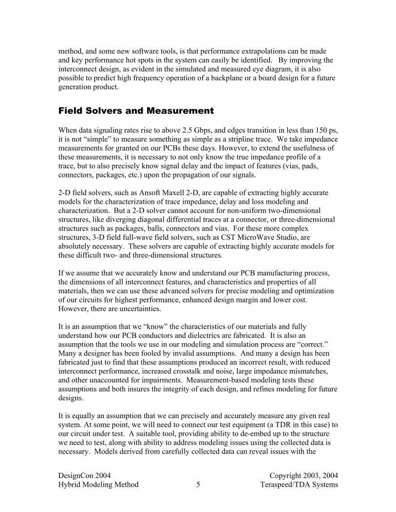
contains 0-80 UNF tapped screw holes for ease of mounting on a PCB. Rather than populate large boards with many hundreds of expensive SMA connectors for testing, a few connectors can be mounted and moved from location to location, thereby reducing overall test cost, yet maintaining test launch quality. To use this SMA, it was necessary to create a reliable procedure to ensure that the launch was of the highest quality and bandwidth possible. In doing so, there are several degrees of freedom available for optimization. First, the layer that is launched into can be chosen for best performance. If the SMA is mounted on the top layer of a PCB and launched into the lowest stripline layer, this configuration reduces the via stub length to its minimum, which increase bandwidth, as is a well-known observation. Conversely, in order to accurately launch into the highest stripline layer, the SMA may be placed on the bottom layer of the PCB. Second, the size of the via clearance holes (antipads) on each layer can be modified to adjust the capacitance and impedance of the structure. Finally, the position of a ground via ring around the transition via can be adjusted to provide 50 ohm impedance for the overall structure. On our first attempt at optimization, Ansoft 3D, a quasi-static field solver, was used to analyze the structure as we modified antipad and ground via sizing. Because the solver uses the quasi-static approximation, no full-wave electromagnetic field effects were analyzed. This proved to be a major problem with this methodology. Optimization consisted of altering the structure until overall impedance from the top layer through to the stripline trace was calculated to be as close to 50 ohms as possible. Figure 2 shows the result of this optimization. A fairly large diameter via separation of approximately 185 mils was found to be optimal for these simulations.
Figure 2 – Ansoft 3D optimized launch pattern.
DesignCon 2004 Copyright 2003, 2004 Hybrid Modeling Method 8 Teraspeed/TDA Systems

TDR measurement of this structure was made using a Tektronix TDS8000/80E04 TDR with TDA Systems IConnect® and is shown in Figure 3. Several things may be determined from this plot. The impedance of the board is measured to be 48.3 ohms. The worst-case launch disruption due to the SMA, vias and antipads is between 56.4 ohms and 48.3 ohms. The launch is primarily “inductive”; that is, it is higher impedance than the nominal 50 ohms. And finally, there is some ringing that can be seen in the higher resolution plot shown later in Figure 11.
Figure 3 – Original SMA TDR profile.
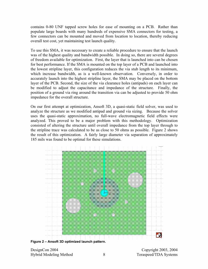
This is not a “bad” launch at all when compared to others we have measured and will be shown later in this paper in Figure 15. But we suspected that there was more room for further improvement using a full-wave electromagnetic approach. Ringing in the connector launch area was the cue that something interesting was going on in this region. Subsequently, a model of the SMA transition was built in CST MicroWave Studio, a Finite Integration Technique 3D time domain field solver and simulation environment. This particular SMA transition was used to benchmark the solver against measurements, to develop confidence in the software and in these types of optimization procedures. Figures 4, 5 and 6 show various views of the modeled SMA transition. Included in the modeling are all via, pad, plane, metal and dielectric structures of the board and SMA, along with all excitation ports. Since a CAD model of the SMA was not available, measurements of the smooth transition area were made and used for modeling purposes. More accurate modeling would require mechanical CAD models for the male and female portion of the SMA. But since we were interested in the performance of PCB transition, this was not a major issue.
DesignCon 2004 Copyright 2003, 2004 Hybrid Modeling Method 9 Teraspeed/TDA Systems

Figure 4 – Original SMA launch perspective view.
Figure 5 – Original SMA launch side view.
DesignCon 2004 Copyright 2003, 2004 Hybrid Modeling Method 10 Teraspeed/TDA Systems
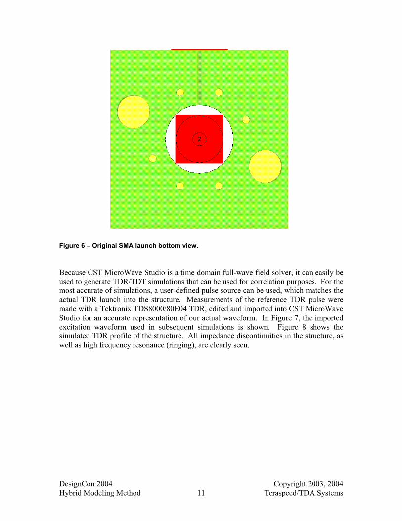
Figure 6 – Original SMA launch bottom view. Because CST MicroWave Studio is a time domain full-wave field solver, it can easily be used to generate TDR/TDT simulations that can be used for correlation purposes. For the most accurate of simulations, a user-defined pulse source can be used, which matches the actual TDR launch into the structure. Measurements of the reference TDR pulse were made with a Tektronix TDS8000/80E04 TDR, edited and imported into CST MicroWave Studio for an accurate representation of our actual waveform. In Figure 7, the imported excitation waveform used in subsequent simulations is shown. Figure 8 shows the simulated TDR profile of the structure. All impedance discontinuities in the structure, as well as high frequency resonance (ringing), are clearly seen.
DesignCon 2004 Copyright 2003, 2004 Hybrid Modeling Method 11 Teraspeed/TDA Systems
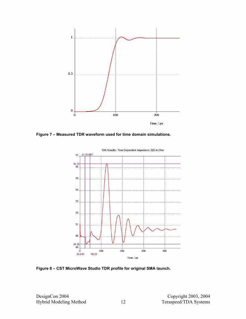
Figure 7 – Measured TDR waveform used for time domain simulations.
Figure 8 – CST MicroWave Studio TDR profile for original SMA launch.
DesignCon 2004 Copyright 2003, 2004 Hybrid Modeling Method 12 Teraspeed/TDA Systems

Comparing Structures Using Measurement-based Methods TDA Systems IConnect® can be used to both de-embed the TDR stimulus to the DUT SMA-stripline trace and generate a true impedance profile from the voltage profile reported by the TDR instrument. Even in simple cases, multiple impedances generate reflections that mask the true impedance profile, making it impossible to model with distributed or lumped components. Generating a true impedance profile is usually the first step in the measurement-based modeling process, since it indicates how the topology of the model should be constructed. It is also an important step in evaluating and comparing different structures. This can be done even before a suitable model is generated and simulated. For example, Figure 9 illustrates a bad launch where the true impedance profile, or Zline, varies from 25 ohms to 68 ohms and there are major capacitive and inductive impedance discontinuities. The initial capacitive discontinuity matches the topology of the launch since a long and wide via was used for the SMA launch.
Figure 9 – Representative of a “Bad” SMA Impedance Profile
Measurement-based Behavioral Modeling Behavioral models accurately represent the time and frequency domain behavior of the interconnects up to the bandwidth of the acquiring TDR instrument. Figure 10 illustrates an example of using MeasureXtractor™ for modeling the original SMA launch and the entire signal path through another board via a connector. A total of
DesignCon 2004 Copyright 2003, 2004 Hybrid Modeling Method 13 Teraspeed/TDA Systems
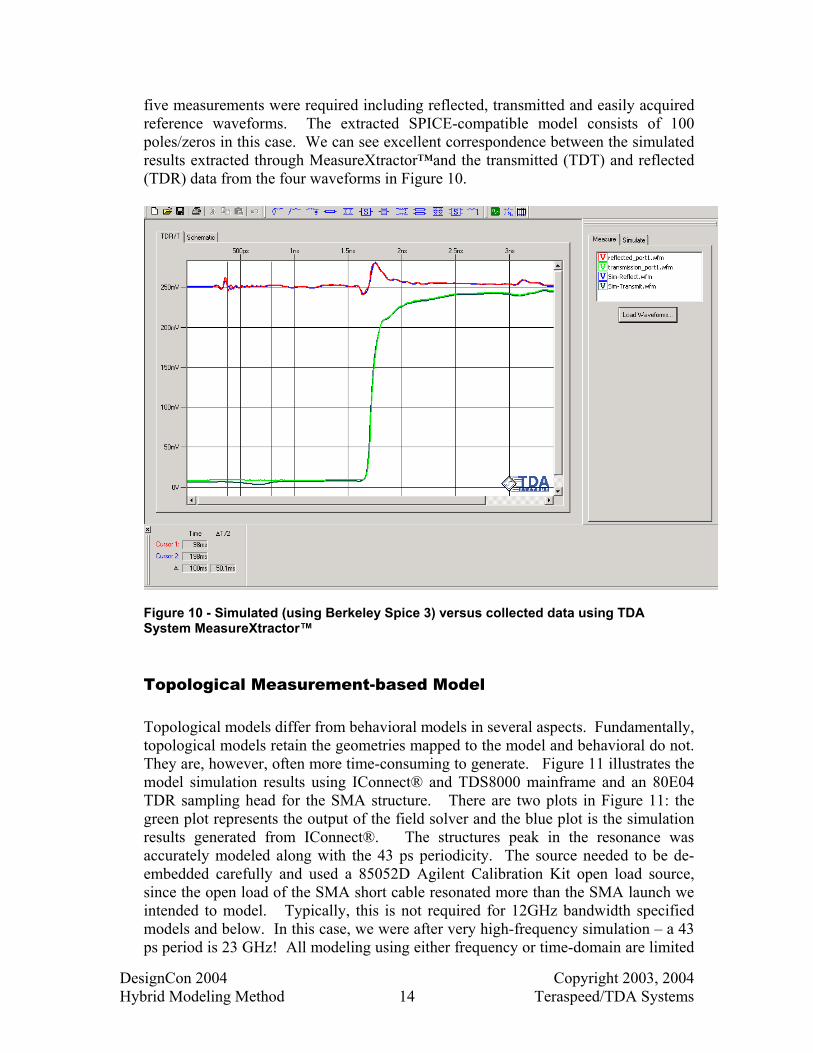
five measurements were required including reflected, transmitted and easily acquired reference waveforms. The extracted SPICE-compatible model consists of 100 poles/zeros in this case. We can see excellent correspondence between the simulated results extracted through MeasureXtractor™and the transmitted (TDT) and reflected (TDR) data from the four waveforms in Figure 10.
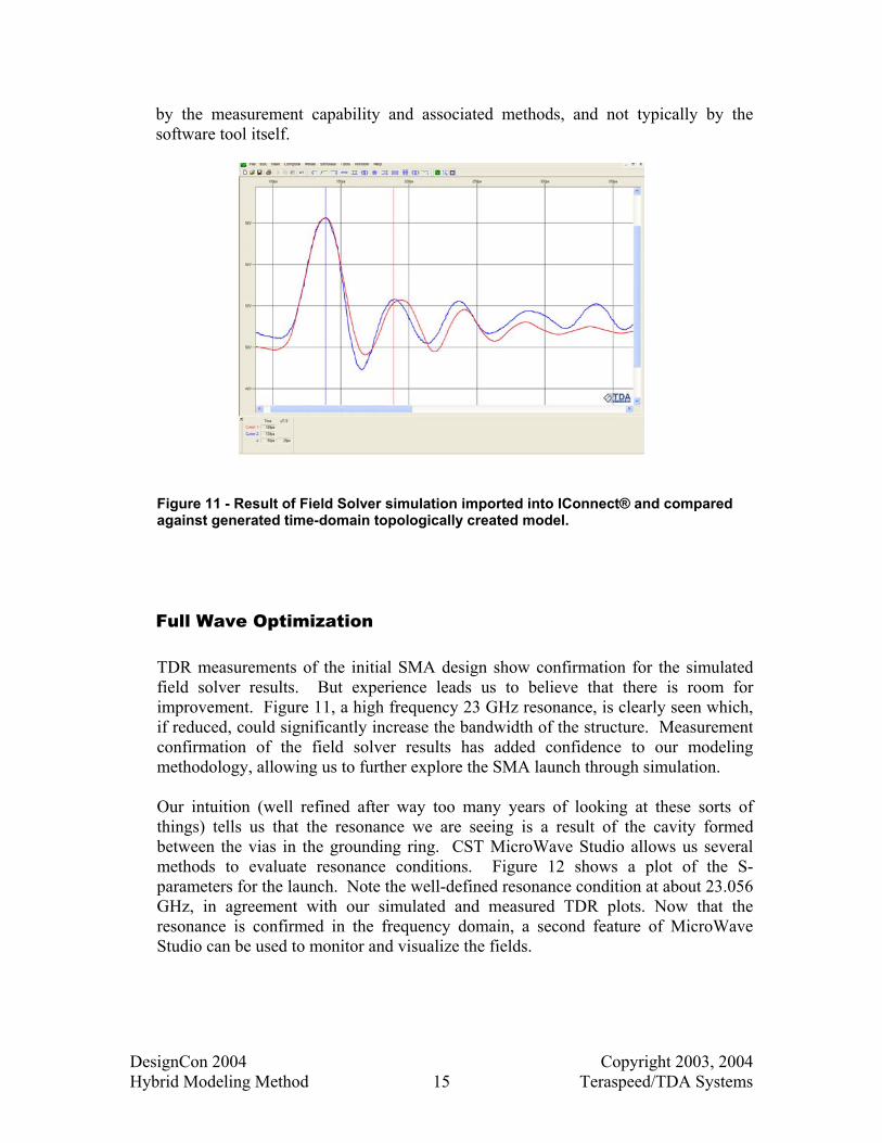
Figure 10 - Simulated (using Berkeley Spice 3) versus collected data using TDA System MeasureXtractor™ Topological Measurement-based Model Topological models differ from behavioral models in several aspects. Fundamentally, topological models retain the geometries mapped to the model and behavioral do not. They are, however, often more time-consuming to generate. Figure 11 illustrates the model simulation results using IConnect® and TDS8000 mainframe and an 80E04 TDR sampling head for the SMA structure. There are two plots in Figure 11: the green plot represents the output of the field solver and the blue plot is the simulation results generated from IConnect®. The structures peak in the resonance was accurately modeled along with the 43 ps periodicity. The source needed to be de-embedded carefully and used a 85052D Agilent Calibration Kit open load source, since the open load of the SMA short cable resonated more than the SMA launch we intended to model. Typically, this is not required for 12GHz bandwidth specified models and below. In this case, we were after very high-frequency simulation – a 43 ps period is 23 GHz! All modeling using either frequency or time-domain are limited
DesignCon 2004 Copyright 2003, 2004 Hybrid Modeling Method 14 Teraspeed/TDA Systems
by the measurement capability and associated methods, and not typically by the software tool itself.
Figure 11 - Result of Field Solver simulation imported into IConnect® and compared against generated time-domain topologically created model.
Full Wave Optimization TDR measurements of the initial SMA design show confirmation for the simulated field solver results. But experience leads us to believe that there is room for improvement. Figure 11, a high frequency 23 GHz resonance, is clearly seen which, if reduced, could significantly increase the bandwidth of the structure. Measurement confirmation of the field solver results has added confidence to our modeling methodology, allowing us to further explore the SMA launch through simulation. Our intuition (well refined after way too many years of looking at these sorts of things) tells us that the resonance we are seeing is a result of the cavity formed between the vias in the grounding ring. CST MicroWave Studio allows us several methods to evaluate resonance conditions. Figure 12 shows a plot of the S-parameters for the launch. Note the well-defined resonance condition at about 23.056 GHz, in agreement with our simulated and measured TDR plots. Now that the resonance is confirmed in the frequency domain, a second feature of MicroWave Studio can be used to monitor and visualize the fields.
DesignCon 2004 Copyright 2003, 2004 Hybrid Modeling Method 15 Teraspeed/TDA Systems

Figure 11 - S-parameter sweep of original SMA transition. Figure 12 shows a plot of an E-field monitor at 23.056 GHz. The resonant field pattern can be clearly seen, bounded on all sides by the ground vias of the structure. Our intuition was correct. As the signal field transitions from the SMA contact on the top layer through the board, it passes down a via, where it turns the corner and attaches itself to trace. During this “turn of the corner,” there is a break in the signal return path due to a transition from coaxial mode to stripline mode. It is this “mode conversion” where some energy in the signal is lost and converted to “parallel plate mode” energy, which is able to propagate along the planes as a circular wave front. This wave front is clearly seen with our field monitor as it hits the boundary of the vias and begins to reflect backwards. Ansoft 3D optimization assumed that the excitation frequency was below that which causes resonant conditions. This is clearly not the case for our SMA launch. But CST MicroWave Studio has the ability to perform optimization of complex structures such as these with all full-wave characteristics. The degrees of freedom for optimization that we discussed above were then used as parameters in this structure. Antipad size on each layer and ground via locations were parameterized and allowed to vary during multiple optimization runs.
DesignCon 2004 Copyright 2003, 2004 Hybrid Modeling Method 16 Teraspeed/TDA Systems

Figure 11 – E-field monitor at 23.056 GHz Figure 12 shows the top view of the original vs. the optimized launch design. Since we are ultimately concerned with reducing reflections off the structure in the time domain, return loss measurements can be used to guide optimization. In our case, minimum S11 in the frequency range from 10 GHz to 30 GHz was specified as the criteria used by the MicroWave Studio optimizer. The results for the final launch structure are shown in Figure 13. When compared to the previous “good” SMA transition profile, several features of the “optimized” transition are apparent. First, the ground via ring diameter has been reduced significantly. Second, by decreasing the via ring diameter, the cavity resonant frequency has been increased to just below 40 GHz, almost a 2X performance improvement. And finally, insertion loss over the operating SMA connector frequency range of 0 Hz to 26.5 GHz has been reduced significantly.
DesignCon 2004 Copyright 2003, 2004 Hybrid Modeling Method 17 Teraspeed/TDA Systems

Figure 12 – Original vs. optimized SMA launch design.
DesignCon 2004 Copyright 2003, 2004 Hybrid Modeling Method 18 Teraspeed/TDA Systems

Figure 13 – Optimized SMA launch S-parameter sweep.
Figure 14 shows a close-up of the IConnect® measured TDR profile for the Teraspeed-optimized SMA-to-stripline transition. On first glance, it seems that the impedance profile ranges from 48 ohms to 53.5 ohms. However, further investigation shows that the large 53.5 ohm impedance discontinuity was internal to the SMA connector. A discontinuity exists at the mating surface between the male connector on the cable and the female receptacle on Molex SMA. After taking this into account, the optimized SMA transition impedance profile is seen to be 48 ohms to 51.5 ohms, or approximately 50 ohms +/- 4%. This SMA to stripline transition actually outperforms the connector itself!
DesignCon 2004 Copyright 2003, 2004 Hybrid Modeling Method 19 Teraspeed/TDA Systems
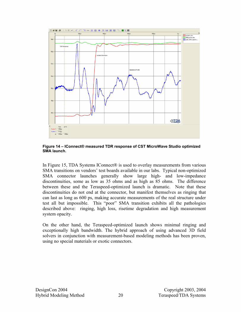
Figure 14 – IConnect® measured TDR response of CST MicroWave Studio optimized SMA launch.
In Figure 15, TDA Systems IConnect® is used to overlay measurements from various SMA transitions on vendors’ test boards available in our labs. Typical non-optimized SMA connector launches generally show large high- and low-impedance discontinuities, some as low as 35 ohms and as high as 85 ohms. The difference between these and the Teraspeed-optimized launch is dramatic. Note that these discontinuities do not end at the connector, but manifest themselves as ringing that can last as long as 600 ps, making accurate measurements of the real structure under test all but impossible. This “poor” SMA transition exhibits all the pathologies described above: ringing, high loss, risetime degradation and high measurement system opacity. On the other hand, the Teraspeed-optimized launch shows minimal ringing and exceptionally high bandwidth. The hybrid approach of using advanced 3D field solvers in conjunction with measurement-based modeling methods has been proven, using no special materials or exotic connectors.
DesignCon 2004 Copyright 2003, 2004 Hybrid Modeling Method 20 Teraspeed/TDA Systems

Figure 15 - IConnect® measured comparison of various SMA launches. The Teraspeed launch is about 50 Ohms +/- 2 Ohms.
DesignCon 2004 Copyright 2003, 2004 Hybrid Modeling Method 21 Teraspeed/TDA Systems

DesignCon 2004 Copyright 2003, 2004 Hybrid Modeling Method 22 Teraspeed/TDA Systems
Closing The Loop And Getting It Right The combination of solver-based modeling methods and measurement-based modeling methods is formidable. Modeling, simulation and measurement are each enhanced when we combine them into an advanced design methodology. Measurements and measured model extraction can be used for the modeling of existing systems, but for future designs, our methods are most efficient when we do not have to build test prototypes every time. When we utilize measurements to test our modeling assumptions and the accuracy of our tools, we provide a calibration to the design process that is unsurpassed. At the simplest level, a TDR pulse may be compared between simulation and measurement. But for more advanced performance studies, a measure-extracted behavioral SPICE model is used in simulation to compare with field solver modeled results. This provides the feedback to “close the loop” for confirmation of, and correction to, the modeling assumptions. Once we have verified our solver methods with measurement, confidence in our final results increases. Changes can be made to designs, with increased density, higher data rates and lower cost. Ultimately, design iterations can be reduced and total development cycles are decreased. The debate is over. Combining field solver and measurement-based methods push the design process into a new realm. This realm does not require multiple design and fabrication iterations to obtain specified performance. The one-time cost of software, test equipment, and process development is easily offset by the hidden costs of multiple design spins, design failures and increased time to market.


![GENERALIZED ANALYTICAL DESIGN OF BROAD- BAND PLANAR … · For the phase shifter section, short-circuited and open-circuited coupled lines have been employed in [10,11] but, there](https://static.fdocuments.us/doc/165x107/5fcce0ec5b71ae364c513b72/generalized-analytical-design-of-broad-band-planar-for-the-phase-shifter-section.jpg)