HX6409/HX6218/HX6136 First-In First-Out Memory/media/aerospace/files/... · First-In First-Out...
21
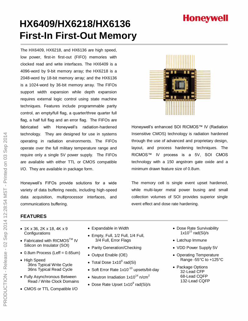
The HX6409, HX6218, and HX6136 are high speed, low power, first-in first-out (FIFO) memories with clocked read and write interfaces. The HX6409 is a 4096-word by 9-bit memory array; the HX6218 is a 2048-word by 18-bit memory array; and the HX6136 is a 1024-word by 36-bit memory array. The FIFOs support width expansion while depth expansion requires external logic control using state machine techniques. Features include programmable parity control, an empty/full flag, a quarter/three quarter full flag, a half full flag and an error flag. The FIFOs are fabricated with Honeywell’s radiation-hardened technology. They are designed for use in systems operating in radiation environments. The FIFOs operate over the full military temperature range and require only a single 5V power supply. The FIFOs are available with either TTL or CMOS compatible I/O. They are available in package form. Honeywell’s FIFOs provide solutions for a wide variety of data buffering needs, including high-speed data acquisition, multiprocessor interfaces, and communications buffering. Honeywell’s enhanced SOI RICMOS™ IV (Radiation Insensitive CMOS) technology is radiation hardened through the use of advanced and proprietary design, layout, and process hardening techniques. The RICMOS™ IV process is a 5V, SOI CMOS technology with a 150 angstrom gate oxide and a minimum drawn feature size of 0.8um. The memory cell is single event upset hardened, while multi-layer metal power busing and small collection volumes of SOI provides superior single event effect and dose rate hardening. FEATURES 1K x 36, 2K x 18, 4K x 9 Configurations Fabricated with RICMOS TM IV Silicon on Insulator (SOI) 0.8um Process (Leff = 0.65um) High Speed 36ns Typical Write Cycle 36ns Typical Read Cycle Fully Asynchronous Between Read / Write Clock Domains CMOS or TTL Compatible I/O Expandable in Width Empty, Full, 1/2 Full, 1/4 Full, 3/4 Full, Error Flags Parity Generation/Checking Output Enable (OE) Total Dose 1x10 6 rad(Si) Soft Error Rate 1x10 -10 upsets/bit-day Neutron Irradiation 1x10 14 n/cm 2 Dose Rate Upset 1x10 9 rad(Si)/s Dose Rate Survivability 1x10 11 rad(Si)/s Latchup Immune VDD Power Supply 5V Operating Temperature Range -55°C to +125°C Package Options 32-Lead CFP 68-Lead CQFP 132-Lead CQFP HX6409/HX6218/HX6136 First-In First-Out Memory PRODUCTION - Release - 02 Sep 2014 12:28:54 MST - Printed on 03 Sep 2014
Transcript of HX6409/HX6218/HX6136 First-In First-Out Memory/media/aerospace/files/... · First-In First-Out...
The HX6409, HX6218, and HX6136 are high speed,
low power, first-in first-out (FIFO) memories with
clocked read and write interfaces. The HX6409 is a
4096-word by 9-bit memory array; the HX6218 is a
2048-word by 18-bit memory array; and the HX6136
is a 1024-word by 36-bit memory array. The FIFOs
support width expansion while depth expansion
requires external logic control using state machine
techniques. Features include programmable parity
control, an empty/full flag, a quarter/three quarter full
flag, a half full flag and an error flag. The FIFOs are
fabricated with Honeywell’s radiation-hardened
technology. They are designed for use in systems
operating in radiation environments. The FIFOs
operate over the full military temperature range and
require only a single 5V power supply. The FIFOs
are available with either TTL or CMOS compatible
I/O. They are available in package form.
Honeywell’s FIFOs provide solutions for a wide
variety of data buffering needs, including high-speed
data acquisition, multiprocessor interfaces, and
communications buffering.
Honeywell’s enhanced SOI RICMOS™ IV (Radiation
Insensitive CMOS) technology is radiation hardened
through the use of advanced and proprietary design,
layout, and process hardening techniques. The
RICMOS™ IV process is a 5V, SOI CMOS
technology with a 150 angstrom gate oxide and a
minimum drawn feature size of 0.8um.
The memory cell is single event upset hardened,
while multi-layer metal power busing and small
collection volumes of SOI provides superior single
event effect and dose rate hardening.
FEATURES
1K x 36, 2K x 18, 4K x 9 Configurations
Fabricated with RICMOSTM
IV Silicon on Insulator (SOI)
0.8um Process (Leff = 0.65um)
High Speed 36ns Typical Write Cycle 36ns Typical Read Cycle
Fully Asynchronous Between Read / Write Clock Domains
CMOS or TTL Compatible I/O
Expandable in Width
Empty, Full, 1/2 Full, 1/4 Full, 3/4 Full, Error Flags
Parity Generation/Checking
Output Enable (OE)
Total Dose 1x10⁶ rad(Si)
Soft Error Rate 1x10⁻¹⁰
upsets/bit-day
Neutron Irradiation 1x10¹⁴
n/cm2
Dose Rate Upset 1x10⁹ rad(Si)/s
Dose Rate Survivability 1x10
11 rad(Si)/s
Latchup Immune
VDD Power Supply 5V
Operating Temperature Range -55°C to +125°C
Package Options 32-Lead CFP 68-Lead CQFP 132-Lead CQFP
HX6409/HX6218/HX6136
First-In First-Out Memory
PR
OD
UC
TIO
N -
Rel
ease
- 0
2 S
ep 2
014
12:2
8:54
MS
T -
Prin
ted
on 0
3 S
ep 2
014

HX6409/HX6218/HX6136
2 www.honeywellmicroelectronics.com
SIMPLIFIED FUNCTIONAL BLOCK DIAGRAM
NMR
NOE NRE
NWE
NHF NE_NF
NQF_NTQF
NEFF
Q[0-8] Q[0-17]
Q[0-35]
D[0-8]
D[0-17]
D[0-35]
CKW
CKR
HX6409/HX6218/HX6136
www.honeywellmicroelectronics.com 3
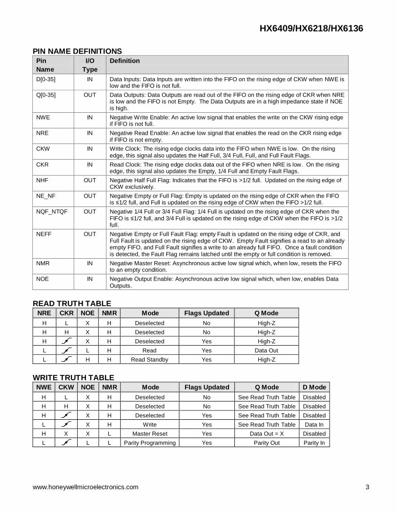
PIN NAME DEFINITIONS
Pin
Name
I/O
Type
Definition
D[0-35] IN Data Inputs: Data Inputs are written into the FIFO on the rising edge of CKW when NWE is low and the FIFO is not full.
Q[0-35] OUT Data Outputs: Data Outputs are read out of the FIFO on the rising edge of CKR when NRE is low and the FIFO is not Empty. The Data Outputs are in a high impedance state if NOE is high.
NWE IN Negative Write Enable: An active low signal that enables the write on the CKW rising edge if FIFO is not full.
NRE IN Negative Read Enable: An active low signal that enables the read on the CKR rising edge if FIFO is not empty.
CKW IN Write Clock: The rising edge clocks data into the FIFO when NWE is low. On the rising edge, this signal also updates the Half Full, 3/4 Full, Full, and Full Fault Flags.
CKR IN Read Clock: The rising edge clocks data out of the FIFO when NRE is low. On the rising edge, this signal also updates the Empty, 1/4 Full and Empty Fault Flags.
NHF OUT Negative Half Full Flag: Indicates that the FIFO is >1/2 full. Updated on the rising edge of CKW exclusively.
NE_NF OUT Negative Empty or Full Flag: Empty is updated on the rising edge of CKR when the FIFO is ≤1/2 full, and Full is updated on the rising edge of CKW when the FIFO >1/2 full.
NQF_NTQF OUT Negative 1/4 Full or 3/4 Full Flag: 1/4 Full is updated on the rising edge of CKR when the FIFO is ≤1/2 full, and 3/4 Full is updated on the rising edge of CKW when the FIFO is >1/2 full.
NEFF OUT Negative Empty or Full Fault Flag: empty Fault is updated on the rising edge of CKR, and Full Fault is updated on the rising edge of CKW. Empty Fault signifies a read to an already empty FIFO, and Full Fault signifies a write to an already full FIFO. Once a fault condition is detected, the Fault Flag remains latched until the empty or full condition is removed.
NMR IN Negative Master Reset: Asynchronous active low signal which, when low, resets the FIFO to an empty condition.
NOE IN Negative Output Enable: Asynchronous active low signal which, when low, enables Data Outputs.
READ TRUTH TABLE
NRE CKR NOE NMR Mode Flags Updated Q Mode
H L X H Deselected No High-Z
H H X H Deselected No High-Z
H X H Deselected Yes High-Z
L L H Read Yes Data Out
L H H Read Standby Yes High-Z
WRITE TRUTH TABLE
NWE CKW NOE NMR Mode Flags Updated Q Mode D Mode
H L X H Deselected No See Read Truth Table Disabled
H H X H Deselected No See Read Truth Table Disabled
H X H Deselected Yes See Read Truth Table Disabled
L X H Write Yes See Read Truth Table Data In
H X X L Master Reset Yes Data Out = X Disabled
L L L Parity Programming Yes Parity Out Parity In
HX6409/HX6218/HX6136
4 www.honeywellmicroelectronics.com
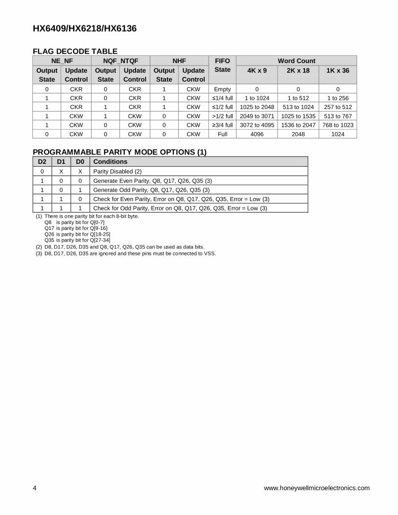
FLAG DECODE TABLE
NE_NF NQF_NTQF NHF FIFO
State
Word Count
Output
State
Update
Control
Output
State
Update
Control
Output
State
Update
Control
4K x 9 2K x 18 1K x 36
0 CKR 0 CKR 1 CKW Empty 0 0 0
1 CKR 0 CKR 1 CKW ≤1/4 full 1 to 1024 1 to 512 1 to 256
1 CKR 1 CKR 1 CKW ≤1/2 full 1025 to 2048 513 to 1024 257 to 512
1 CKW 1 CKW 0 CKW >1/2 full 2049 to 3071 1025 to 1535 513 to 767
1 CKW 0 CKW 0 CKW ≥3/4 full 3072 to 4095 1536 to 2047 768 to 1023
0 CKW 0 CKW 0 CKW Full 4096 2048 1024
PROGRAMMABLE PARITY MODE OPTIONS (1)
D2 D1 D0 Conditions
0 X X Parity Disabled (2)
1 0 0 Generate Even Parity, Q8, Q17, Q26, Q35 (3)
1 0 1 Generate Odd Parity, Q8, Q17, Q26, Q35 (3)
1 1 0 Check for Even Parity, Error on Q8, Q17, Q26, Q35, Error = Low (3)
1 1 1 Check for Odd Parity, Error on Q8, Q17, Q26, Q35, Error = Low (3)
(1) There is one parity bit for each 8-bit byte.
Q8 is parity bit for Q[0-7] Q17 is parity bit for Q[9-16]
Q26 is parity bit for Q[18-25] Q35 is parity bit for Q[27-34]
(2) D8, D17, D26, D35 and Q8, Q17, Q26, Q35 can be used as data bits.
(3) D8, D17, D26, D35 are ignored and these pins must be connected to VSS.

HX6409/HX6218/HX6136
www.honeywellmicroelectronics.com 5
ABSOLUTE MAXIMUM RATINGS (1)
Symbol Parameter Ratings Unit
Min Max
VDD Positive Supply Voltage Referenced to VSS -0.5 6.5 V
VIO Voltage on Any Input or Output Pin Referenced to VSS -0.5 VDD + 0.5 V
IOUT Average Output Current 25 mA
TSTORE Storage Temperature -65 150 C
TSOLDER (2) Soldering Temperature 270 C
PD (3) Package Power Dissipation 2.5 W
PJC Package Thermal Resistance (Junction to Case) 5.0 C/W
VHBM Electrostatic Discharge Protection Voltage (Human Body Model) 2000 V
TJ Junction Temperature 175 C
(1) Stresses in excess of those listed above may result in immediate permanent damage to the device. These are stress ratings only and operation at these levels is not implied. Frequent or extended exposure to absolute maximum conditions may affect device reliability.
(2) Maximum soldering temperature can be maintained for no more than 5 seconds.
(3) IDDSB power + IDDOP power + Output driver power due to external loading must not exceed this specif ication.
RECOMMENDED OPERATING CONDITIONS (1)
Symbol Parameter Limits Unit
Min Typ Max
VDD Positive Supply Voltage Referenced to VSS 4.5 5.0 5.5 V
TC Case Temperature -55 25 125 C
VIO Voltage on Any Input or Output Pin Referenced to VSS -0.3 VDD + 0.3 V
(1) Specifications listed in datasheet apply when operated under the Recommended Operating Conditions unless otherwise specified.

HX6409/HX6218/HX6136
6 www.honeywellmicroelectronics.com
RADIATION HARDNESS RATINGS (1)
Symbol Parameter Environment Conditions Limits (2) Unit
TID Total Ionizing Dose, R-Level 1x10⁵
rad(Si)
Total Ionizing Dose, F-Level 3x10⁵ rad(Si)
Total Ionizing Dose, H-Level 1x10⁶ rad(Si)
DRU Transient Dose Rate Upset Pulse width ≤20ns 1x10⁹ rad(Si)/s
DRS Transient Dose Rate Survivability Pulse width ≤20ns 1x10¹¹
rad(Si)/s
SER (2) Projected Soft Error Rate Geosynchronous orbit during solar
minimum non-flare conditions
behind 100mil Aluminum shield
1x10⁻¹⁰
upsets/bit-day
Neutron Irradiation Damage 1 MeV equivalent energy 1x10¹⁴
n/cm2
(1) Device will not latchup when exposed to any of the specified radiation environments.
(2) Calculated using CREME96.
RADIATION CHARACTERISTICS Total Ionizing Dose Radiation
The SRAM radiation hardness assurance TID level was qualified by
60Co testing, including overdose and
accelerated annealing, per MIL-STD-883 Method 1019. Ongoing assurance is provided by wafer level X-ray testing during manufacturing. Single Event Soft Error Rate
Special process, memory cell, circuit and layout design considerations are included in the SRAM to minimize the impact of heavy ion and proton radiation and achieve small projected SER. These techniques sufficiently harden the SRAM such that cell redundancy and scrubbing are not required to achieve the projected SER. Transient Dose Rate Ionizing Radiation
Many aspects of product design are addressed to handle the high energy levels associated with the transient dose rate events. This allows the SRAM to be capable of writing, reading, and retaining stored
data during and after exposure to a transient dose rate ionizing radiation pulse, up to the DRU specification. The SRAM will also meet functional and timing specifications after exposure to a transient dose rate ionizing radiation pulse up to the DRS specification. Neutron Irradiation Damage
SOI CMOS is inherently tolerant to damage from neutron irradiation. The SRAM meets functional and timing specifications after exposure to the specified neutron fluence. Latchup
The SRAM will not latchup when exposed to any of the above radiation environments when applied under recommended operating conditions. SOI CMOS provides oxide isolation between adjacent PMOS and NMOS transistors and eliminates any potential SCR latchup structures.
PIN CAPACITANCE (1)
Symbol Parameter Max Unit
CIN Input Capacitance 7 pF
COUT Output Capacitance 9 pF
(1) Maximum capacitance is verified as part of initial qualification
only.

HX6409/HX6218/HX6136
www.honeywellmicroelectronics.com 7
POWER PIN ELECTRICAL CHARACTERISTICS
Symbol Parameter Conditions Max Unit
IDDSB Static
Supply Current
VIH = VDD,
VIL = VSS,
Q = High-Z
1 mA
IDDOP (1)(2)(3) Dynamic
Supply Current
Selected
VIH = VDD, VIL = VSS,
Q = High-Z,
CKR = CKW = 1MHz
4k x 9 8 mA
2k x 18 9 mA
1k x 36 12 mA
IDDOP (1)(2)(3) Dynamic
Supply Current
Selected
VIH = VDD, VIL = VSS,
Q = High-Z,
CKR = CKW = 27MHz
4k x 9 280 mA
2k x 18 330 mA
1k x 36 500 mA
IDDOPD (1)(2) Dynamic
Supply Current
Deselected
VIH = VDD, VIL = VSS,
NWE = NRE = VIH,
CKR = CKW = 1MHz,
All other inputs = static
1 mA
IDDOPD (1)(2) Dynamic
Supply Current
Deselected
VIH = VDD, VIL = VSS,
NWE = NRE = VIH,
CKR = CKW = 27MHz,
All other inputs = static
24 mA
IDR Data Retention
Supply Current
VDD = 2.5V 500 uA
(1) All inputs switching. DC average current.
(2) All dynamic operating mode current measurements (IDDOPx) exclude standby mode current (IDDSB). The total power is the
sum of the power from the standby current (IDDSB), dynamic current (IDDOPx) and output driver current driving the output load.
(3) Data inputs are switching at one half the clock speed.
SIGNAL PIN ELECTRICAL CHARACTERISTICS (1)
Symbol Parameter Conditions Min Max Unit
IIN Input Leakage Current VSS ≤ VIN ≤ VDD -1 1 uA
IOZ Output Leakage Current Q = High-Z -10 10 uA
VIL Low-Level Input Voltage CMOS 0.3 x VDD V
TTL 0.8 V
VIH High-Level Input Voltage CMOS 0.7 x VDD V
TTL 2.2 V
VOL Low-Level Output Voltage IOL = 4mA 0.4 V
VOH1 High-Level Output Voltage IOH = -4mA 3.5 V
VOH2 High-Level Output Voltage IOH = -100uA VDD - 0.4 V
(1) Voltages referenced to VSS.

TIMING CHARACTERISTICS (1)(6)
Symbol Parameter Limits Unit
Min Max
TCKW (2) Write Clock Cycle 24 ns
TCKR Read Clock Cycle 36 ns
TCKHR Clock High Read 26 ns
TCKHW Clock High Write 14 ns
TCKL Clock Low Read / Write 10 ns
TA Data Access Time 30 ns
TOH Previous Output Data Hold After NRE High 2 ns
TFH (7) Previous Flag Hold After NRE/NWE High 2 ns
TSD Data Setup 12 ns
THD Data Hold 4 ns
TSEN Enable Setup 8 ns
THEN Enable Hold 2 ns
TOE NOE Low to Output Data Valid 10 ns
TOLZ NOE Low to Output Data in Low-Z 1 ns
TOHZ NOE High to Output Data in High-Z 10 ns
TFD (7) Flag Delay 19.3 ns
TSKEW1 (3)(5) Non-controlling Clock after Controlling Clock 0 ns
TSKEW2 (4)(5) Non-controlling Clock before Controlling Clock 25 ns
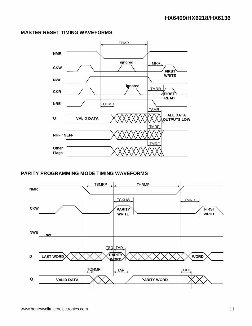
TPMR Master Reset Pulse Width (Low) 25 ns
TOHMR Data Hold from Master Reset Low 2 ns
TMRR Master Reset Recovery 8 ns
TMRF (7) Master Reset High to Flags Valid 17 ns
TAMR Master Reset High to Data Outputs Low 17 ns
TSMRP Parity Program Mode – NMR low Set-up to CKW High 10 ns
THMRP Parity Program Mode – NMR High Hold from CKW High 4 ns
TAP Parity Program Mode – Data Access Time 30 ns
TOHP Parity Program Mode – Data Hold Time from NMR High 2 ns
(1) The timing specifications are referenced to the Timing Input / Output References diagrams and the
Timing Reference Load Circuit diagrams. IBIS models should be used to evaluate timing under application load and conditions.
(2) Guaranteed, but not tested.
(3) For flags that are updated by both CKR and CKW (i.e., NE_NF, NQF_NTQF, NEFF) TSKEW1 is the minimum time a non-controlling clock
can occur after the controlling clock and still not be included in the controlling clock cycle. At less than TSKEW1, inclusion of the non-
controlling clock in the controlling clock cycle is arbitrary.
(4) For flags that are updated by both CKR and CKW (i.e., NE_NF, NQF_NTQF, NEFF) TSKEW2 is the minimum time a non-controlling clock
can occur before the controlling clock and still be included in the controlling clock cycle. At less than TSKEW2, inclusion of the non-
controlling clock in the controlling clock cycle is arbitrary.
(5) The non-controlling clock is the signal which does not have update control of the flags (i.e., CKW is the non-controlling clock when the FIFO
is ≤1/2 full and CKR is the non-controlling clock when the FIFO is >1/2 full). The controlling clock is the signal which has update control of
the flags (i.e., CKW is the controlling clock when the FIFO is >1/2 full, and CKR is the controlling clock when the FIFO is ≤1/2 full).
(6) Timing parameters are shown in Timing Waveforms below.
(7) Flags refers to signals: NHF, NE_NF, NQF_NTQF, NEFF.
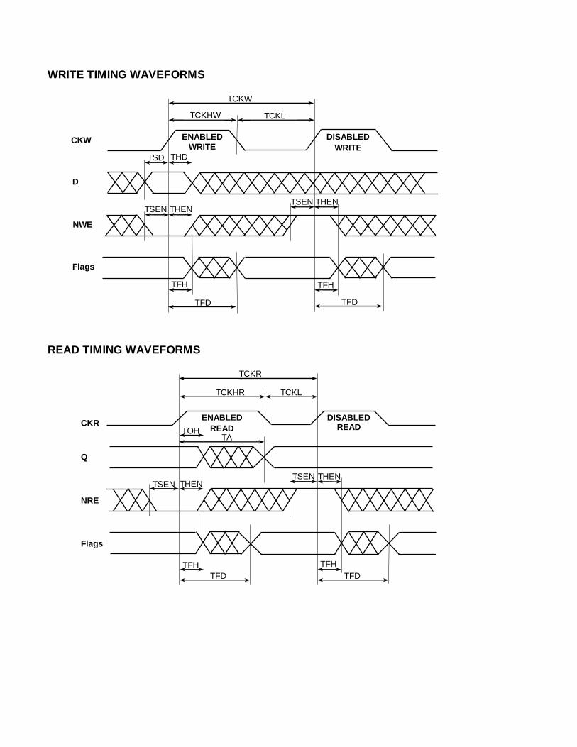
WRITE TIMING WAVEFORMS
READ TIMING WAVEFORMS
TCKR
TCKHR TCKL
TOH TA
TSEN THEN TSEN THEN
TFH
TFD
TFH
TFD
ENABLED
READ
DISABLED READ
CKR
Q
NRE
Flags
TCKW
TCKL TCKHW
TSD THD
TSEN THEN TSEN THEN
TFD TFD
TFH TFH
CKW
D
NWE
Flags
DISABLED
WRITE
ENABLED WRITE

HX6409/HX6218/HX6136
10 www.honeywellmicroelectronics.com
FLAG UPDATE TIMING WAVEFORMS WHEN FIFO IS ≤1/2 FULL
(1) W2 may or may not be included in R1 flag update.
(2) W3 is not included in R1 flag update.
(3) W2 is included in R3 flag update. (4) W3 may or may not be included in R3 flag update.
FLAG UPDATE TIMING WAVEFORMS WHEN FIFO IS >1/2 FULL
(1) R2 may or may not be included in W1 flag update. (2) R3 is not included in W1 flag update.
(3) R2 is included in W3 flag update.
(4) R3 may or may not be included in W3 flag update.
CKR
NWE
CKW
NRE
Other
Flags
NHF
≥TSKEW2 (3) <TSKEW1 (1)
TFD TFD TFD
W1 W3 W4
R2
Low
W2
R1 R3 R4
≥TSKEW1 (2) <TSKEW2 (4)
CKW
NWE
CKR
NRE
Other
Flags
NHF
≥TSKEW2 (3) <TSKEW1 (1)
TFD TFD TFD
R1 R3 R4
W2
High
R2
W1 W3 W4
≥TSKEW1 (2) <TSKEW2 (4)
HX6409/HX6218/HX6136
www.honeywellmicroelectronics.com 11
MASTER RESET TIMING WAVEFORMS
PARITY PROGRAMMING MODE TIMING WAVEFORMS
TSMRP THRMP
TCKHW TMRR
TSD THD
TOHMR TAP TOHP
VALID DATA PARITY WORD
PARITY
WRITE
FIRST
WRITE
PARITY
WORD WORD LAST WORD D
Q
CKW
NWE
NMR
Low
TPMR
TMRR
TMRR
TOHMR
TAMR
TMRF
TMRF
VALID DATA ALL DATA
OUTPUTS LOW
NMR
CKW
NWE
CKR
NRE
Q
NHF / NEFF
Other
Flags
FIRST WRITE
ignored
ignored
FIRST READ

HX6409/HX6218/HX6136
12 www.honeywellmicroelectronics.com
OUTPUT ENABLE TIMING WAVEFORMS
TIMING REFERENCE LOAD CIRCUIT (TTL)
DUT Output
30pF (1)
50ohm
Zo = 50ohm
1.5V
Notes
(1) Set to 5pF for T*Z (Low-Z to High-Z)
timing parameters.
TIMING INPUT / OUTPUT REFERENCES (TTL)
Input Levels (1)
Output Levels
1.5V (2)
High-Z (4)
High-Z (4)
3V
0V
90%
10%
90%
10%
VOHss - 0.1V (2)(3)
VOLss + 0.1V (2)(3)
1.5V (2)
VOHss - 0.1V (2)(3)
VOLss + 0.1V (2)(3)
Notes
(1) Input rise and fall times = 1ns between 90% and 10% levels.
(2) Timing parameter reference voltage level.
(3) ss: Low-Z VOH and VOL steady-state output voltage.
(4) High-Z output pin pulled to 1.5V by Reference Load Circuit.
TIMING REFERENCE LOAD CIRCUIT (CMOS)
DUT Output
30pF (1)
50ohm
Zo = 50ohm
VDD/2
Notes
(1) Set to 5pF for T*Z (Low-Z to High-Z)
timing parameters.
TIMING INPUT / OUTPUT REFERENCES (CMOS)
Input Levels (1)
Output Levels
VDD/2 (2)
High-Z (4)
High-Z (4)
VDD - 0.5V
VSS + 0.5V
90%
10%
90%
10%
VOHss - 0.1V (2)(3)
VOLss + 0.1V (2)(3)
VDD/2 (2)
VOHss - 0.1V (2)(3)
VOLss + 0.1V (2)(3)
Notes
(1) Input rise and fall times = 1ns between 90% and 10% levels.
(2) Timing parameter reference voltage level.
(3) ss: Low-Z VOH and VOL steady-state output voltage.
(4) High-Z output pin pulled to VDD/2 by Reference Load Circuit.
TOHZ TOE
TOLZ
NOE
Q
CKR
NRE
READ M+1
VALID DATA WORD M VALID DATA WORD M+1
Low

HX6409/HX6218/HX6136
www.honeywellmicroelectronics.com 13
FUNCTIONAL DESCRIPTION FIFO Write / Read Operation
Writing data on the input pins (D) into the FIFO is controlled by a write clock (CKW) and a write enable pin (NWE). When NWE is asserted, data is written into the FIFO on the rising edge of the CKW signal. While NWE is held active, data is continually written into the FIFO on each CKW cycle. CKW will update the flags it controls independent of the NWE state. Reading data from the FIFO onto the output pins (Q) is controlled by a read clock (CKR) and a read enable pin (NRE). When NRE is asserted, data is read from the FIFO on the rising edge of the CKR signal. While NRE is held active, data is continually read from the FIFO on each CKR cycle. CKR will update the flags it controls independent of the NRE state. The read (CKR) and write (CKW) clocks may be tied together for single-clock operation or the two clocks may be run completely asynchronous to one another. The FIFOs have an output enable pin (NOE) that controls the Low-Z and High-Z states of the Q output drivers. The FIFOs have a master reset pin (NMR) to reset the FIFO to an empty condition. It is also used as a gateway to program the parity mode setting. Master Reset
Upon power up, the FIFO must be reset with a Master Reset (NMR) cycle. This causes the FIFO to enter the empty condition where the Empty (NE_NF) and 1/4 Full or 3/4 Full (NQF_NTQF) flags are low, and the Half Full (NHF) and Empty or Full Fault (NEFF) flags are high. The outputs (Q) are set to low and the flags are set to the empty state TAMR/TMRF respectively after NMR goes high. During a master reset, NMR must be held low for at least TPMR and NWE and NRE are to be held high while NMR is low. Valid data is maintained for TOHMR after NMR goes low. When NMR is brought high there is a master reset recovery time (TMRR) before rising edges of CKW or CKR can occur. Parity Programming
There is a parity bit for every 8 data bits. Parity is presented on Data Outputs: Q8, Q17, Q26 and Q35. The type of parity is programmed with the D[0-2] bits during a parity programming mode write operation. See the Programmable Parity Options Table for a description of the FIFO parity modes. Data present on D[0-2] during a parity programming mode write will determine whether the FIFO will generate or check
even or odd parity for the data present on D[0-7], D[9-16], D[18-25] and D[27-34]. When parity is enabled then D8, D17, D26 and D35 inputs are ignored. If the FIFO is programmed for parity checking it will compare the parity of Q[0-7], Q[9-16], Q[18-25] and Q[27-34] to the stored parity bit and outputs the results on Q8, Q17, Q26 and Q35, respectively. High is a match, low is a mismatch. When parity is disabled the FIFO writes all of the D input pins and the read outputs to all of the Q output pins. A parity programming operation occurs when Master Reset (NMR) is low and Write Enable (NWE) is low. To write the parity mode word, D[0-2] into the FIFO programming register, NMR must be setup low at least TSMRP prior to the Write Clock (CKW) going high and NMR must be held low THRMP after CKW goes high. CKW must be held high for at least TCKH. The parity mode word needs to setup TSD prior to CKW going high and held THD after CKW goes high. The parity mode word is put on the Data Outputs Q[0-2] TAP after CKW goes high and the parity mode word is held TOHP after NMR goes high. When NMR is brought high there is a master reset recovery time (TMRR) before the next rising edge on CKW can occur. Full Flag / Empty Flag The Empty / Full Flag (NE_NF) is a combined functionality flag for specifying an empty or full FIFO. NE_NF will go low when the FIFO is empty or full and will go high when the FIFO is not empty or not full. Assessment of whether the FIFO is full or empty is done by evaluating the state of the Half Full Flag (NHF) (see Flag Decode Table). When the FIFO is >1/2 full the NE_NF flag state is updated on the rising edge of CKW. The NE_NF flag will go low when the FIFO is written to a full condition. Write operations are inhibited whenever the FIFO is full regardless of the state of NWE. To re-enable the write requires at least one read cycle followed by one CKW cycle to reset the NE_NF flag to a non-full state after which a write is no longer inhibited. A full FIFO that is read will be described as full until either CKW goes high or the FIFO becomes ≤1/2 full. Transitioning between full and almost full flag states requires a clock cycle on CKW to update the flag to the current state. The flag is updated independent of the state of NWE; so a data write is not necessary to
HX6409/HX6218/HX6136
14 www.honeywellmicroelectronics.com
update the flags to correctly describe the state of the FIFO. When the flags indicate the FIFO is full even though data has been read from the FIFO, two CKW cycles are required to write data into the FIFO. The first CKW cycle clears the NE_NF flag to indicate the FIFO is not full and to stop inhibiting writes. The second CKW cycle with NWE low inputs the data. The first CKW cycle is the latent or flag update cycle since it does not alter the data in the FIFO or the count (number of words in the FIFO). It simply updates the NE_NF flag. In order for the NE_NF flag to update appropriately for the non-full condition the read cycle must occur at least TSKEW2 before the latent or flag update cycle in order to guarantee that the read will be included in the count when CKW is cycled to update NE_NF.
When the FIFO is ≤1/2 full the NE_NF flag state is updated on the rising edge of CKR. The NE_NF flag will go high when the FIFO is read to an empty condition. Read operations are inhibited whenever the FIFO is empty regardless of the state of NRE. To re-enable the read requires at least one write cycle followed by one CKR cycle to reset the NE_NF flag to a non-empty state after which a read is no longer inhibited. An empty FIFO that is written will be described as empty until either CKR goes high or the FIFO becomes >1/2 full. Transitioning between empty and almost empty flag states requires a clock cycle on CKR to update the flag to the current state. The flag is updated independent of the state of NRE; so a data read is not necessary to update the flags to correctly describe the state of the FIFO. When the flags indicate the FIFO is empty even though data has been written to the FIFO, two CKR cycles are required to read data from the FIFO. The first CKR cycle clears the NE_NF flag to indicate the FIFO is not empty and to stop inhibiting reads. The second CKR cycle with NRE low outputs the data. The first CKR cycle is the latent or flag update cycle since it does not alter the data in the FIFO or the count (number of words in the FIFO). It simply updates the NE_NF flag. In order for the NE_NF flag to update appropriately for the non-empty condition the write cycle must occur at least TSKEW2 before the latent or flag update cycle in order for the FIFO to guarantee that the write will be included in the count when CKR is cycled to update NE_NF.
Half Full Flag
The Half Full Flag (NHF) is a functionality flag for ≤1/2 full or >1/2 full. NHF will go low when the FIFO is >1/2 full and will go high when the FIFO is ≤1/2 full. NHF is updated exclusively on the rising edge of CKW. 1/4 Full / 3/4 Full Flag
The 1/4 Full / 3/4 Full Flag (NQF_NTQF) is a combined functionality flag for ≤1/4 full and ≥3/4 full. NQF_NTQF will go low when the FIFO is ≤1/4 full or ≥3/4 full and will go high when the FIFO is not ≤1/4 full or ≥3/4 full. Assessment of whether the FIFO is ≤1/4 or ≥3/4 full is done by evaluating the state of the Half Full Flag (NHF) (see Flag Decode Table). NQF_NTQF is updated on the rising edge of CKR if the FIFO is ≤1/2 full and is updated on the rising edge of CKW if the FIFO is >1/2 full (see Flag Decode Table). Empty or Full Fault Flag
The Empty or Full Fault Flag (NEFF) is a combined functionality flag for Empty or Full faults. An Empty fault signifies a read to an already empty FIFO, and a full fault signifies a write to an already full FIFO. NEFF will go low when either of these fault conditions occurs. NEFF is updated on the rising edge of CKR if the FIFO is empty and NEFF is updated on the rising edge of CKW if the FIFO is full. Signal Integrity
As a general design practice, one should have good signal integrity which means input signals that are free of noise, glitches and ringing with rising and falling edges of ≤10ns. More specifically, an input is considered to have good signal integrity when the input voltage monotonically traverses the region between VIL and VIH in ≤10ns. This is especially important in a selected and enabled state. When the device is selected and enabled, the last transitioning input for the desired operation must have good signal integrity to maintain valid operation. The transitioning inputs that bring the device into and out of a selected and enabled state must also have good signal integrity to maintain valid operation. When the device is deselected and/or disabled, inputs can have poor signal integrity and even float as long as the inputs that are defining the deselected and/or disabled state stay within valid VIL and VIH voltage levels. However, floating inputs for an extended period of time is not recommended.

RELIABILITY
For many years Honeywell has been producing integrated circuits that meet the stringent reliability requirements of space and defense systems. Honeywell has delivered hundreds of thousands of QML parts since first becoming QML qualified in 1990. Using this proven approach Honeywell will assure the reliability of the products manufactured with the SOI CMOS process technology. This approach includes adhering to Honeywell’s Quality Management Plan for:
• Designing in reliability by establishing electrical rules based on wear out mechanism characterization performed on specially designed test structures (electromigration, TDDB, hot carriers, bias temperature instability and radiation).
• Utilizing a structured and controlled design process.
• Statistically controlling wafer fabrication process with a continuous defect reduction process.
• Performing individual wafer lot acceptance through process monitor testing (includes radiation testing).
• Using characterized and qualified packages.
• Performing thorough product testing program based on MIL-PRF-38535 and MIL-STD 883.
SCREENING AND CONFORMANCE
INSPECTION The product test flow includes screening units with the applicable flow (Engineering Model, Class V or equivalent, Class Q or equivalent) and the appropriate periodic or lot Conformance Testing (Groups A, B, C, D, and E). Both the wafer process and the products are subject to periodic or lot based Technology Conformance Inspection (TCI) / Quality Conformance Inspection (QCI) tests as defined by Honeywell’s Quality Management Plan. Conformance Summary
Group A General Electrical Tests
Group B Mechanical – Resistance to Solvents, Bond Strength, Die Shear, Solderability
Group C Life Tests - 1000 hours at 125C or equivalent
Group D Package Related Mechanical Tests – Physical Dimensions, Lead Integrity, Thermal Shock, Temp Cycle, Moisture Resistance, Seal, Mechanical Shock, Vibration, Acceleration, Salt Atmosphere, Internal Water Vapor, Adhesion of Lead Finish
Group E Radiation Tests
PACKAGE FEATURES
Feature Description Description Description
Designation T D F
Type 32-lead flat pack 68-lead flat pack 132-lead flat pack
Body Construct multi-layer
ceramic (Al2O3)
multi-layer
ceramic (Al2O3)
multi-layer
ceramic (Al2O3)
VDD, VSS Planes Yes Yes Yes
Lid Construct Kovar Kovar Kovar
Lid Electrical Connection VSS VSS VSS
VDD to VSS Chip Capacitors (Caps) (1) 4 x 0.039uF User Option (1) -
(1) Default configuration is without package capacitors. Contact Honeywell for part ordering information if capacitors are desired.

HX6409/HX6218/HX6136
16 www.honeywellmicroelectronics.com
PIN LIST FOR HX6409
Pin Signal Pin Signal Pin Signal Pin Signal Pin Signal Pin Signal
1 VSS 7 Q5 13 NQF_NTQF 19 NRE 25 D6 31 D0
2 Q0 8 Q6 14 NHF 20 CKW 26 D5 32 VDD
3 Q1 9 Q7 15 NE_NF 21 NWE 27 D4
4 Q2 10 Q8 16 VSS 22 NMR 28 D3
5 Q3 11 NOE 17 VDD 23 D8 29 D2
6 Q4 12 NEFF 18 CKR 24 D7 30 D1
PIN LIST FOR HX6218
Pin Signal Pin Signal Pin Signal Pin Signal Pin Signal Pin Signal
1 CKR 13 D17 25 VSS 37 Q1 49 Q11 61 VSS
2 NRE 14 D16 26 D8 38 Q2 50 Q12 62 VDD
3 CKW 15 D15 27 D7 39 Q3 51 Q13 63 NOE
4 NWE 16 D14 28 D6 40 Q4 52 VDD 64 NEFF
5 NMR 17 VDD 29 D5 41 Q5 53 VSS 65 NQF_NTQF
6 VDD 18 VSS 30 D4 42 Q6 54 Q14 66 NHF
7 VSS 19 D13 31 D3 43 Q7 55 Q15 67 NE_NF
8 VSS 20 D12 32 D2 44 Q8 56 Q16 68 VDD
9 VSS 21 D11 33 D1 45 VSS 57 Q17
10 VDD 22 D10 34 D0 46 VDD 58 VDD
11 VDD 23 D9 35 VDD 47 Q9 59 VDD
12 VDD 24 VDD 36 Q0 48 Q10 60 VDD
PIN LIST FOR HX6136
Pin Signal Pin Signal Pin Signal Pin Signal Pin Signal Pin Signal
1 VSS 23 CKW 45 NC 67 VSS 89 Q2 111 Q19
2 NC 24 NC 46 D25 68 NC 90 NC 112 Q20
3 NC 25 NWE 47 NC 69 D8 91 Q3 113 NC
4 NC 26 NC 48 D24 70 D7 92 NC 114 Q21
5 NOE 27 NMR 49 VSS 71 D6 93 Q4 115 VDD
6 NC 28 NC 50 VDD 72 NC 94 Q5 116 VSS
7 NEFF 29 NC 51 D23 73 D5 95 Q6 117 Q22
8 NQF_NTQF 30 NC 52 D22 74 D4 96 Q7 118 Q23
9 NHF 31 NC 53 D21 75 D3 97 Q8 119 Q24
10 NC 32 NC 54 D20 76 NC 98 NC 120 Q25
11 NE_NF 33 VSS 55 D19 77 D2 99 VSS 121 Q26
12 NC 34 VDD 56 D18 78 NC 100 VDD 122 Q27
13 NC 35 D35 57 D17 79 D1 101 Q9 123 Q28
14 NC 36 D34 58 D16 80 NC 102 Q10 124 NC
15 NC 37 D33 59 D15 81 D0 103 Q11 125 Q29
16 VSS 38 D32 60 D14 82 VSS 104 Q12 126 Q30
17 VDD 39 D31 61 D13 83 VDD 105 Q13 127 Q31
18 NC 40 D30 62 D12 84 NC 106 Q14 128 Q32
19 CKR 41 D29 63 D11 85 Q0 107 Q15 129 Q33
20 NC 42 D28 64 D10 86 NC 108 Q16 130 Q34
21 NRE 43 D27 65 D9 87 Q1 109 Q17 131 Q35
22 NC 44 D26 66 VDD 88 NC 110 Q18 132 VDD
NC pin must be connected to VSS.

HX6409/HX6218/HX6136
www.honeywellmicroelectronics.com 17
PACKAGE DIAGRAMS 32-Lead Flat Pack, Designation = T

HX6409/HX6218/HX6136
18 www.honeywellmicroelectronics.com
68-Lead Flat Pack, Designation = D

HX6409/HX6218/HX6136
www.honeywellmicroelectronics.com 19
132-Lead Flat Pack, Designation = F

HX6409/HX6218/HX6136
20 www.honeywellmicroelectronics.com
NOT APPLICABLE.
HX6409/HX6218/HX6136
www.honeywellmicroelectronics.com 21
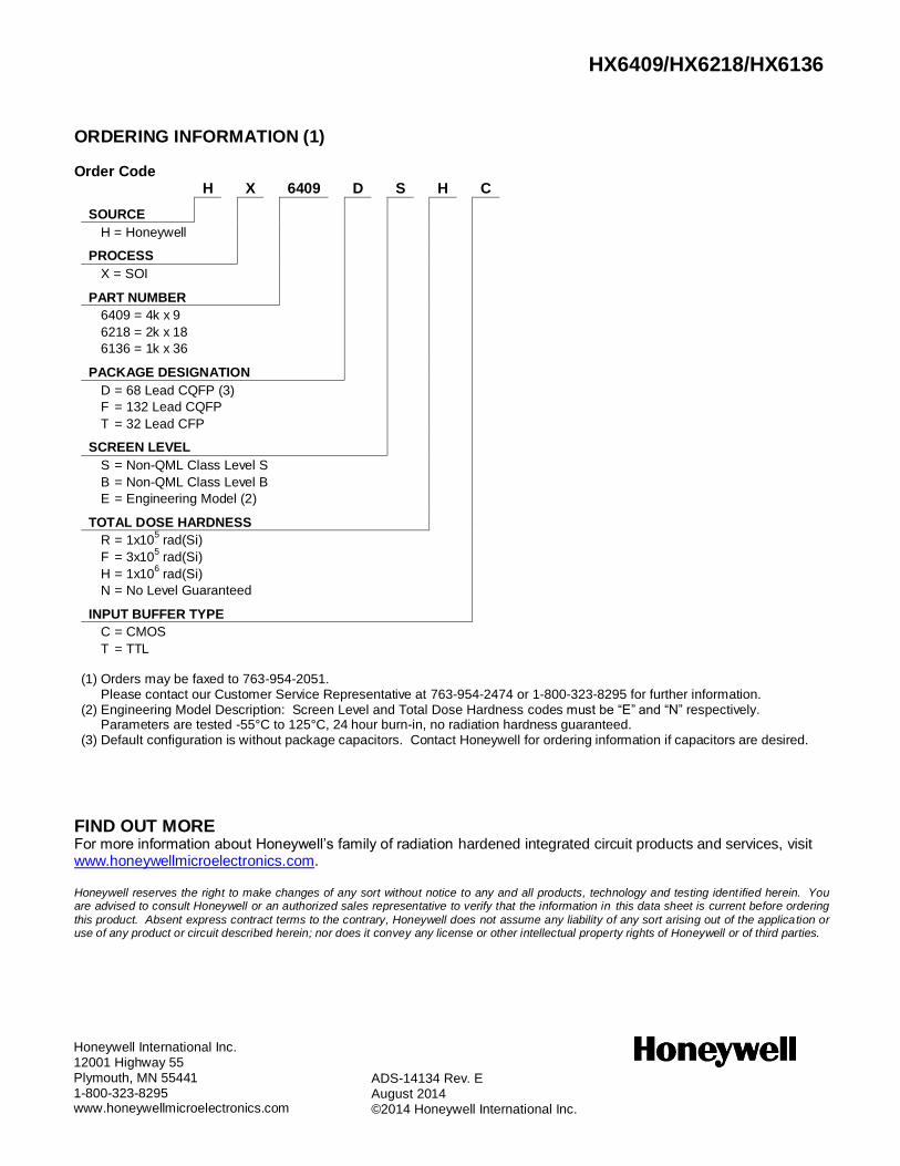
ORDERING INFORMATION (1)
Order Code
H X 6409 D S H C
SOURCE
H = Honeywell
PROCESS
X = SOI
PART NUMBER
6409 = 4k x 9
6218 = 2k x 18
6136 = 1k x 36
PACKAGE DESIGNATION
D = 68 Lead CQFP (3)
F = 132 Lead CQFP
T = 32 Lead CFP
SCREEN LEVEL
S = Non-QML Class Level S
B = Non-QML Class Level B
E = Engineering Model (2)
TOTAL DOSE HARDNESS
R = 1x10⁵ rad(Si)
F = 3x10⁵ rad(Si)
H = 1x10⁶ rad(Si)
N = No Level Guaranteed
INPUT BUFFER TYPE
C = CMOS
T = TTL
(1) Orders may be faxed to 763-954-2051.
Please contact our Customer Service Representative at 763-954-2474 or 1-800-323-8295 for further information. (2) Engineering Model Description: Screen Level and Total Dose Hardness codes must be “E” and “N” respectively.
Parameters are tested -55°C to 125°C, 24 hour burn-in, no radiation hardness guaranteed. (3) Default configuration is without package capacitors. Contact Honeywell for ordering information if capacitors are desired.
FIND OUT MORE For more information about Honeywell’s family of radiation hardened integrated circuit products and services, visit www.honeywellmicroelectronics.com. Honeywell reserves the right to make changes of any sort without notice to any and all products, technology and testing ident ified herein. You are advised to consult Honeywell or an authorized sales representative to verify that the information in this data sheet is current before ordering
this product. Absent express contract terms to the contrary, Honeywell does not assume any liability of any sort arising out of the application or use of any product or circuit described herein; nor does it convey any license or other intellectual property rights of Honeywell or of third parties.
ADS-14134 Rev. E August 2014 ©2014 Honeywell International Inc.
Honeywell International Inc. 12001 Highway 55 Plymouth, MN 55441 1-800-323-8295 www.honeywellmicroelectronics.com