HTADC12 (Die Deliverable) High Temperature 12-Bit, …/media/aerospace/files/... · HTADC12 (Die...
12
HTADC12 (Die Deliverable) High Temperature 12-Bit, 100kSPS A/D Converter The HTADC12 is a high temperature12-bit, 100kSPS, analog-to-digital converter with on-chip buffered voltage reference and an on-chip analog input buffer. The HTADC12 uses a Successive Approximation Register (SAR) architecture that does not require an input sample-and-hold amplifier to provide 12-bit resolution at 100 kSPS data rates over the full operating temperature range of -55 O C to +225 O C. The HTADC12 is fabricated on a high temperature Silicon On Insulator (SOI) CMOS process with very low power consumption. The input of the HTADC12 allows for easy interfacing to sensors for data conversion applications. The direct input supports 0V to 2.5V signals and there is also an on- chip buffer to allow for full 5V input signals. The product is offered with both a serial and parallel digital output interface. The switched capacitor charge-redistribution DAC architecture does not require a sample-and-hold input stage. It is well suited for both multiplexed systems that switch full-scale voltage levels in successive channels and also for sampling single-channel inputs at frequencies up to and well beyond the Nyquist rate. An internal clock is used to operate the HTADC12. The digital output data is presented in straight binary output format. There are three output formats: 12 bit parallel, two 8 bit parallel, and serial. FEATURES Monolithic 12-Bit, 100 kSPS A/D Converter Operating temperature range of -55 O C to +225 O C +5 V operation On-chip high temperature voltage reference Buffered voltage reference output pin On-chip analog input buffer Straight binary output data Typical INL of +/- 0.6 LSB at 225 O C Parallel 12-bit output or serial output Input flexibility to use internal reference or off-chip reference. Die Deliverable The HTADC12 die can be incorporated in multi-chip packages. Low Power The HTADC12, at 10 mW, consumes a fraction of the power of presently available ADCs in existing monolithic solutions.
Transcript of HTADC12 (Die Deliverable) High Temperature 12-Bit, …/media/aerospace/files/... · HTADC12 (Die...

HTADC12 (Die Deliverable) High Temperature 12-Bit, 100kSPS A/D Converter
The HTADC12 is a high temperature12-bit, 100kSPS,
analog-to-digital converter with on-chip buffered voltage
reference and an on-chip analog input buffer. The
HTADC12 uses a Successive Approximation Register
(SAR) architecture that does not require an input
sample-and-hold amplifier to provide 12-bit resolution at
100 kSPS data rates over the full operating temperature
range of -55OC to +225OC.
The HTADC12 is fabricated on a high temperature
Silicon On Insulator (SOI) CMOS process with very low
power consumption.
The input of the HTADC12 allows for easy interfacing to
sensors for data conversion applications. The direct
input supports 0V to 2.5V signals and there is also an on-
chip buffer to allow for full 5V input signals. The product
is offered with both a serial and parallel digital output
interface.
The switched capacitor charge-redistribution DAC
architecture does not require a sample-and-hold input
stage. It is well suited for both multiplexed systems that
switch full-scale voltage levels in successive channels
and also for sampling single-channel inputs at
frequencies up to and well beyond the Nyquist rate. An
internal clock is used to operate the HTADC12.
The digital output data is presented in straight binary
output format. There are three output formats: 12 bit
parallel, two 8 bit parallel, and serial.
FEATURES
Monolithic 12-Bit, 100 kSPS A/D Converter
Operating temperature range of -55OC to +225OC
+5 V operation
On-chip high temperature voltage reference
Buffered voltage reference output pin
On-chip analog input buffer
Straight binary output data
Typical INL of +/- 0.6 LSB at 225OC
Parallel 12-bit output or serial output
Input flexibility to use internal reference or off-chip reference.
Die Deliverable
The HTADC12 die can be incorporated in multi-chip packages.
Low Power The HTADC12, at 10 mW, consumes a fraction of the power of presently available ADCs in existing monolithic solutions.
HTADC12
2 www.hightempsolutions.com
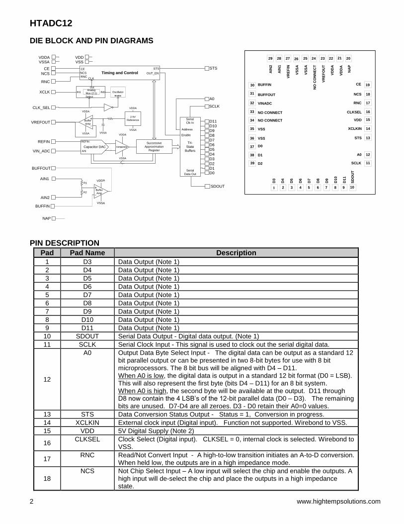
DIE BLOCK AND PIN DIAGRAMS
PIN DESCRIPTION
Pad Pad Name Description
1 D3 Data Output (Note 1)
2 D4 Data Output (Note 1)
3 D5 Data Output (Note 1)
4 D6 Data Output (Note 1)
5 D7 Data Output (Note 1)
6 D8 Data Output (Note 1)
7 D9 Data Output (Note 1)
8 D10 Data Output (Note 1)
9 D11 Data Output (Note 1)
10 SDOUT Serial Data Output - Digital data output. (Note 1)
11 SCLK Serial Clock Input - This signal is used to clock out the serial digital data.
12
A0 Output Data Byte Select Input - The digital data can be output as a standard 12 bit parallel output or can be presented in two 8-bit bytes for use with 8 bit microprocessors. The 8 bit bus will be aligned with D4 – D11. When A0 is low, the digital data is output in a standard 12 bit format (D0 = LSB). This will also represent the first byte (bits D4 – D11) for an 8 bit system. When A0 is high, the second byte will be available at the output. D11 through D8 now contain the 4 LSB’s of the 12-bit parallel data (D0 – D3). The remaining bits are unused. D7-D4 are all zeroes. D3 - D0 retain their A0=0 values.
13 STS Data Conversion Status Output - Status = 1, Conversion in progress.
14 XCLKIN External clock input (Digital input). Function not supported. Wirebond to VSS.
15 VDD 5V Digital Supply (Note 2)
16 CLKSEL Clock Select (Digital input). CLKSEL = 0, internal clock is selected. Wirebond to
VSS.
17 RNC Read/Not Convert Input - A high-to-low transition initiates an A-to-D conversion.
When held low, the outputs are in a high impedance mode.
18 NCS Not Chip Select Input – A low input will select the chip and enable the outputs. A
high input will de-select the chip and place the outputs in a high impedance state.
Tri-
State
BuffersCapacitor DAC
REFIN
AIN
Comparator
VSSA
VDDA
VSSA
VDDA
Successive
Approximation
Register
R2
R1
Buffer
Amp
+
-
VSSA VSSA
VDDA
VSSA
Analog
Mux (2:1)IN1 IN0
Select
Out
Oscillator
Enable
2.5V
Reference
Timing and Control
CLK
CE
RNC
STS
OUT_EN
D11
D10
D9
D8
D7
D6
D5
D4
D3
D2
D1D0
VDDAVSSA
Enable
STS
VDDVSS
RNC
CE
XCLK
CLK_SEL
VREFOUT
REFIN
VIN_ADC
BUFFIN
AIN1
AIN2
NCSNCS
NAP
BUFFOUT
Address
Serial
Clk In
Serial
Data Out
SCLK
A0
SDOUT
Buffer
Amp
+
-
VDDA
29 28 27 26 25 24 23 21
STS
A0
D1
1
1
D1
0
0
D9
9
D8
8
D7
7
D6
6
D5
5
D4
4
D3
3
22
30
31
32
33
34
35
36
37
39
38
1 2 3 4 5 6 7 8 10 9
20
19
18
17
16
15
14
13
11
12
SD
OU
T
SCLK
XCLKIN
VDD
NCS
RNC
CLKSEL
CE
VD
DA
VD
DA
VR
EF
OU
T
T
NO
CO
NN
EC
T
CO
NN
EC
T
VS
SA
A
VS
SA
A
VR
EF
IN
N
AIN
1
1
AIN
2
2 NA
P
P
VSS
D1
D2
VSS
NO CONNECT
BUFFOUT
VINADC
NO CONNECT
BUFFIN
D0

HTADC12
3 www.hightempsolutions.com
Pad Pad Name Description
19 CE Chip Enable Input - A high input will enable the chip and enable the outputs. A
low input will disable the chip and place the outputs in a high impedance state.
20 NAP Power down control (digital input). NAP=0 for normal operation.
21 VDDA 5V Analog Supply (Note 2)
22 VDDA 5V Analog Supply (Note 2)
23 VREFOUT VREF Buffered Output. Nominally 2.5V buffered output of on-chip voltage
reference. May be connected to VREFIN on the board.
24 NO CONNECT Leave pad open
25 VSSA Analog Ground (Note 2)
26 VSSA Analog Ground (Note 2)
27 VREFIN Voltage Reference Input. May be connected to VREFOUT or to an external
voltage reference.
28 AIN1 Analog Input - Input to buffer amplifier
29 AIN2 Analog Input - Input to buffer amplifier
30 BUFFIN Analog Input - Input to negative terminal of the buffer amplifier
31 BUFFOUT Analog Output - Output of the buffer amplifier
32 VINADC Analog Voltage Into A/D Converter
33 NO CONNECT Leave pad open
34 NO CONNECT Leave pad open
35 VSS Digital Ground (Note 2)
36 VSS Digital Ground (Note 2)
37 D0 Data Output. (Note 1)
38 D1 Data Output. (Note 1)
39 D2 Data Output. (Note 1)
Notes (1) The data outputs are tri-state drivers and may be put into a high impedance state according to truth table.
(2) Where wirebond pads have the same labeling they are electrically connected on-chip (VDD, VDDA, VSS, and VSSA).
VDDA and VDD should be connected externally to the same potential. VSSA and VSS should also be connected externally
to the same potential. VDDA and VDD are separated on-chip to reduce inductive supply noise coupling to the analog front-
end (from on-chip logic switching and/or output transients). VSSA and VSS are separated on-chip for the same reason.
TRUTH TABLE
CE NCS RNC A0 Operation Outputs
0 x x x None High Impedance
x 1 x x None High Impedance
0 0 x Initiate conversion High Impedance
1 0 x Initiate conversion High Impedance
1 0 x Initiate conversion High Impedance
1 0 1 x Enable serial output Enabled
1 0 1 0 Enable 12-bit parallel output (8 MSBs are read here when using 8-bit bus option)
Enabled
1 0 1 1 Enable 4 LSBs + 4 trailing zeroes, all super-imposed on 8 MSB outputs (8-bit bus option)
Enabled

HTADC12
4 www.hightempsolutions.com
ABSOLUTE MAXIMUM RATINGS (1)
Name Parameter Rating Units
Min Max VDD Supply Voltage (2) -0.1 6.0 Volts
VPIN Voltage on Any Pin (2) -0.1 VDD+0.1 Volts
TSTORE Storage Temperature -55 300 °C
IOUT Average Output Current 50 mA
ESD Electrostatic Discharge Protection Voltage (3) 750 V
PJB Die Thermal Resistance (Top Side Junction to Backside of Die)
0.54 OC/W
(1) Stresses in excess of those listed above may result in immediate permanent damage to the device. These are stress ratings only,
and operation at these levels is not implied. Frequent or extended exposure to absolute maximum conditions may affect device reliability.
(2) Voltage referenced to VSS = 0V. (3) Class 1 Electrostatic Discharge (ESD) input protection voltage per MIL-STD-883, Method 3015
RECOMMENDED OPERATING CONDITIONS (1)
Symbol Parameter Description
Min Typ Max
VDD Supply Voltage 4.75 5.0 5.25 Volts
Temp Op Operating Temperature -55 225 °C
VPIN Voltage on Any Pin 0.0 VDD Volts
VREFIN Input Voltage Reference 0.0 2.5 Volts (1) Voltages referenced to Vss = 0V.
DC ELECTRICAL CHARACTERISTICS (2)
Symbol Parameter Conditions(1) Limits Units
Min Typ Max
IDDA VDD Quiescent
Current
No external load on
VREFOUT
2.5 5 mA
IDD VDD Quiescent Current 150 250 µA
IDDA NAP Quiescent Current VDDA NAP=1 (on), No external
load on VREFOUT.
500 1000 µA
IDD NAP Quiescent Current VDD 150 250 µA
IOZ Output Tri-State Leakage Output High Impedance -5 +5 uA
VIL Low Level Input Voltage Digital I/O signals 20
% of
VDD
(V)
VIH High Level Input Voltage Digital I/O signals 80
% of
VDD
(V)
VOH High Level Output Voltage Sourcing 4mA Current VDD- 0.5 V
VOL Low Level Output Voltage Sinking 4mA Current VSS+ 0.5 V
IIL Input current at VIN=VSS Digital I/O signals -1 +1 µA
IIH Input current at VIN=VDD Digital I/O signals -1 +1 µA
(1) Unless otherwise specified, specifications apply over the full operating temperature range from -55C to 225C, VDDA externally connected to VDD = 5V, VSSA externally connected to VSS = 0V.
(2) Electrical testing of wafers/die is conducted at 25OC only.

HTADC12
5 www.hightempsolutions.com
ELECTRICAL PERFORMANCE CHARACTERISTICS (6)
Symbol Parameter Conditions(1) Limits Units
Min Typ Max
# of Bits Resolution (2) 12 Bits
INL Integral Non-Linearity -2.8 +2.8 LSB
DNL Differential Non-Linearity -1.0 +1.8 LSB
Offset Offset Error VIN value @ VOUT =
Voltage equivalent to
0.0LSB (from Linear
regression), T=25C
-5 0 +5 LSB
OS_TC Offset Error Tempco (7) -5 +5 ppm/°C
FS_ERR Full Scale Error Maximum change in full
scale calibration
VREFIN = 2.5V, T=25°C
-0.3 +0.3 % of FS
FS_TC FS Error Tempco (7) -3 +3 ppm/°C
PSRA Power Supply Rejection
Magnitude of Output Code -1 1 LSB
PSRD Power Supply Rejection
-1 1 LSB
VREFOUT Reference Output Voltage 2.49 2.51 V
∆ VRO-TIME VREFOUT Drift with time T=225°C, ∆t=1000 hours (2) -3 +3 mV
∆VRO
/∆VDDA
VREFOUT Line Regulation -
DC
-1 +1 mV/V
∆VRO /∆IO VREFOUT Load Regulation –
DC (4)
0.0 mA ≤ Iout ≤ +8.0 mA 0.5 mV/mA
VRN VREFOUT Noise (2) f = 0.1Hz to 10kHz 110 µV rms
FSCLK Serial Clock Frequency Cload = 10pF, Note 3 40 MHz
TWAKEUP Wake-up time from NAP (ADC
ready to convert) (5)
30 µs
VOSAA Auxiliary Amplifier Input Offset
Voltage
-3 ±1 +3 mV
BWAA Auxiliary Amp Unity Gain
Bandwidth (5)
Cload = 40pf 3 5 MHz
∆ R/R Aux Amp Input Resistor
Divider (/2)Matching (5)
-0.1 +0.1 %
Notes (1) Unless otherwise specified, specifications apply over the full operating temperature range from -55C to 225C, VDDA externally connected
to VDD =5V, VSSA externally connected to VSS = 0V. (2) Guaranteed by initial qualification test. (3) Maximum serial clock frequency listed is for a 10pF load on SDOUT. For greater capacitive loads, a lower clock frequency must be used. For
Cload = 100pF, Fsclk = 10 MHz is the recommended maximum. (4) VREF_OUT can provide source current only. (5) Guaranteed by design. (6) Electrical testing of wafers/die is conducted at 25OC only. (7) Not tested at wafer or die level. Guaranteed by lot sample test of packaged parts.

HTADC12
6 www.hightempsolutions.com
SIGNAL DEFINITION
ANALOG INPUT OPTIONS The analog input signal may be connected directly to the VIN ADC input or go through a buffer amplifier. Direct into VINADC The input range can be from 0V to VREFIN. This input is high impedance but should be driven by a low impedance source. Input Utilizing Buffer Amp The HTADC12 has an integrated buffer amplifier which can be used to condition the input signal. The access to the amplifier input and output pins provides the ability to create various conditioning circuits. Both input terminals and the output terminal of the amplifier are available. On the positive terminal, the AIN1 and AIN2 inputs are configured to allow the signal to be divided by 2 through a resistor divider (with either AIN1 or AIN2 connected to VSSA = 0V). This provides the ability to use signals from 0V to 5V. The negative input terminal and output are on separate pins allowing additional circuits to be implemented. The maximum output value shall be VREFIN. The internal resistor values are 20k ohms. This output may then be connected to VIN ADC which has an input range of 0V to VREFIN (or 2.5V maximum). The output buffer may also be used as a unity-gain input buffer by applying the analog input to both AIN1 and AIN2.
TRI-STATE OUTPUT CONTROL The digital outputs are tri-state drivers. They are controlled by the CE, NCS, and RNC. To have the outputs active, CE and RNC must be high and NCS must be low. RNC The RNC signal is used to trigger an A-to-D Conversion by a high-to-low transition.
STS This signal is a status indicator for the validity of the output data. STS is high while a conversion is in progress.
NAP
The NAP input may be used to put all analog circuitry except VREF into a low-current mode, saving power during inactive periods.
FUNCTIONAL DESCRIPTION The A-to-D converter block consists of a 12-bit successive approximation analog-to-digital converter using an internal 12-bit capacitive charge re-distribution DAC. Conversions are initiated by a high-to-low transition on the RNC input. The analog input voltage range is from 0V to VREF_IN. While the conversion is in progress, the Status output (STS) is high and the parallel data outputs (D0 through D11) are in a high impedance state. When the conversion is complete, the data is made available on the parallel data output pins (D0 through D11). STS goes low indicating that data is ready. A complete A/D conversion cycle requires 38 clock cycles. The nominal internal clock frequency is 4 MHz. ADC Clocking: The internal A/D clock is nominally 4 MHz, and is approximately temperature and supply independent. At the nominal clock frequency the ADC throughput is approximately 100KSamples/sec. Use of an external clock on XCLKIN (Pin 14) is not supported. Voltage Reference Options: The full-scale input range of the ADC is 0V to VREFIN. The 12-bit ADC has an internal, buffered reference source VREFOUT. VREFOUT is within 2.49V to 2.51V over all conditions (-55OC to +225OC). The reference buffer is designed to provide a low-impedance output capable of settling within the sampling time of the ADC when operated with the 4MHz clock. To use this reference connect VREFOUT directly to VREFIN. Do not add decoupling capacitors at this connection. The capacitance on VREFOUT should be minimized. An external voltage reference may be used instead of the internal reference source. In that case, the external source may be connected directly to VREFIN and VREFOUT may be left un-connected. ADC Converter Control: Four signals are used to control the ADC.
- Conversion Control: CE, NCS, and RNC - Output Buffer Control: CE, NCS, and RNC - Output Format: A0
Conversion Control
R2
R1
Buffer
Amp
+
-
VDDA
VSSA
BUFFIN
AIN1
AIN2
BUFFOUT

HTADC12
7 www.hightempsolutions.com
It is recommended to use RNC as the signal to trigger the conversion and read functions. CE and NCS should be used as enables. Refer to timing diagrams.
However, the CE, NCS, and RNC have equivalent signal functions. A conversion can be initiated by a
transition on the any of the control lines, as shown in the Truth Table.
Once a conversion is started, it can be terminated and restarted by reasserting the appropriate control lines.
RECOMMENDED OPERATING MODES There are two main methods of operating the HTADC12, Open Loop and Closed Loop.
Open Loop
The HTADC12 can be used in an open loop mode in which the enable pins are held at a steady value and conversions are triggered by RNC. The output data is available and read when STS goes low. To trigger another conversion, only RNC has to be driven low.
(1) CE is held high and NCS is held low.
(2) RNC is pulsed from a high to a low value which starts the conversion. RNC returns high before the conversion is completed.
(3) The STS signal will then go to a high value.
(4) When the conversion is complete, STS will go low indicating the data is available on the output bus.
(5) The next conversion is started with another pulse on the RNC line.
OPEN LOOP TIMING DIAGRAM
Symbol Parameter Min Typ Max Units
T1 STS Delay From RNC 100 ns
T2 Low RNC Pulse Width 20 ns
T3 Conversion Time (1) 9 10 11.5 µs
T4 STS Delay After Data Buffer Turn-On 50 80 110 ns
T5 Data Valid Hold Time after RNC low 20 ns
Notes
(1) Conversion Time based on 38 cycles of the internal 4MHz clock.
NCS
RNC
STS
HIGH DATA OUT DATA OUT
IMPEDANCE DATA VALID
CE HIGH
LOW
T4
T1
T2
T5
T3

HTADC12
8 www.hightempsolutions.com
Closed Loop – Processor Controlled This mode requires control of the input enable pins CE, NCS, and RNC. The STS signal will be used to notify the processor that a conversion is complete. The processor then changes the state of RNC to read the output data. Assuming that CE is high and NCS is low, a typical conversion sequence may be:
(1) CE and NCS are set to activate the device.
(2) RNC is then changed from a high to a low value which starts the conversion.
(3) The STS signal will then go to a high value.
(4) When the conversion is complete, STS will go low. This will be detected by the processor/controller.
(5) The controller then sets RNC back to a high level and signaling the data can be read at the outputs.
(6) Following the read, CE and NCS are then set to disable the device and put the outputs into a high impedance state.
CLOSED LOOP TIMING DIAGRAM
Symbol Parameter Min Typ Max Units
T7 Setup Time NCS To RNC 0 5 ns
T6 Setup Time CE To RNC 0 5 ns
T1 STS Delay From RNC 100 ns
T3 Conversion Time 9 10 11.5 µs
T8 READ Delay After Enable 100 ns
T5 Data Valid Hold Time 20 ns
CE
NCS
RNC
STS
HIGH DATA OUT DATA OUT
IMPEDANCE DATA VALID
T6
T7
T1 T3
T8 T5

HTADC12
9 www.hightempsolutions.com
Data Output Formats: There are three output formats: 12 bit parallel, two 8 bit parallel, and serial.
Serial Output Control: Conversions in the serial
output mode are initiated identically to the parallel
output mode described above. The serial data output,
SDO, is enabled identically as well.
Valid data becomes available at SDO immediately at
the end of the conversion cycle (slightly prior to STS).
Data is output MSB first, and advances one bit position
with each SCLK falling edge.
Rising SCLK edges may be used to clock serial data
into the master.
SCLK activity occurring other than when SDO is
properly enabled for read is ignored.
The parallel data can be presented as either 12 straight binary bits or configured for a “two-byte READ” for use with 8 bit processor busses.
12-Bit Data Readout in 8-Bit Systems: The HTADC12’s 12-bit parallel data output can be read out by an 8-bit system in two 8-bit bytes. In this mode, the
8 MSB bit positions of the 12-bit output are utilized as the 8-bit bus. Address control of the byte of interest is handled by the logic state of the A0 control line.
- When A0=0, the output data assumes its normal 12-bit format with bits D11-D4 of the 12-bit word forming the 1st data byte. - When A0=1, bits D3-D0 followed by 4 logic zeroes are superimposed onto the 8 MSB bit positions, forming the 2nd data byte.
SERIAL OUTPUT TIMING DIAGRAM
Symbol Parameter Min Typ Max Units
T4 STS Delay After Data Buffer Turn-On 50 80 110 ns
T9 Rising Edge of First Clock 0 ns
Data Output Pins
Data Output Values
AO = 0 (READ bits D4 – D11)
AO = 1 (READ bits D0 – D3)
D11 D11 D3
D10 D10 D2
D9 D9 D1
D8 D8 D0
D7 D7 “0”
D6 D6 “0”
D5 D5 “0”
D4 D4 “0”
D3 D3 D3
D2 D2 D2
D1 D1 D1
D0 D0 D0
8 Bit Bus
CE
NCS
RNC
STS
SCLK
SDO D11 D10 D9 D8 D7 D2 D3 D4 D5 D6 D0 D1
LSB MSB
zeros Hi - Z
HIGH
HIGH
LOW
T4 T9
HTADC12
10
www.hightempsolutions.com
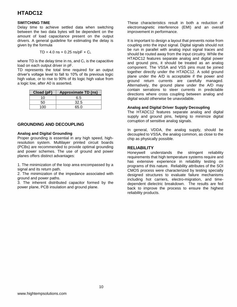
SWITCHING TIME Delay time to achieve settled data when switching between the two data bytes will be dependent on the amount of load capacitance present on the output drivers. A general guideline for estimating the delay is given by the formula
TD = 4.0 ns + 0.25 ns/pF × CL
where TD is the delay time in ns, and CL is the capacitive load on each output driver in pF. TD represents the total time required for an output driver’s voltage level to fall to 10% of its previous logic high value, or to rise to 90% of its logic high value from a logic low, after A0 is asserted.
Cload (pF) Approximate TD (ns)
10 6.5
50 32.5
100 65.0
GROUNDING AND DECOUPLING Analog and Digital Grounding Proper grounding is essential in any high speed, high-resolution system. Multilayer printed circuit boards (PCBs) are recommended to provide optimal grounding and power schemes. The use of ground and power planes offers distinct advantages: 1. The minimization of the loop area encompassed by a signal and its return path. 2. The minimization of the impedance associated with ground and power paths. 3. The inherent distributed capacitor formed by the power plane, PCB insulation and ground plane.
These characteristics result in both a reduction of electromagnetic interference (EMI) and an overall improvement in performance. It is important to design a layout that prevents noise from coupling onto the input signal. Digital signals should not be run in parallel with analog input signal traces and should be routed away from the input circuitry. While the HTADC12 features separate analog and digital power and ground pins, it should be treated as an analog component. The VSSA and VSS pins must be joined together directly under the HTADC12. A solid ground plane under the A/D is acceptable if the power and ground return currents are carefully managed. Alternatively, the ground plane under the A/D may contain serrations to steer currents in predictable directions where cross coupling between analog and digital would otherwise be unavoidable. Analog and Digital Driver Supply Decoupling The HTADC12 features separate analog and digital supply and ground pins, helping to minimize digital corruption of sensitive analog signals. In general, VDDA, the analog supply, should be decoupled to VSSA, the analog common, as close to the chip as physically possible.
RELIABILITY Honeywell understands the stringent reliability requirements that high temperature systems require and has extensive experience in reliability testing on programs of this nature. Reliability attributes of the SOI CMOS process were characterized by testing specially designed structures to evaluate failure mechanisms including hot carriers, electro-migration, and time-dependent dielectric breakdown. The results are fed back to improve the process to ensure the highest reliability products.

HTADC12
11 www.hightempsolutions.com
DIE OUTLINE DIMENSIONS
Notes:
(1) Backside metalization is gold. (2) Metalization on the pads is aluminum. (3) The backside of the die is connected to VSS.
ASSEMBLY INFORMATION Die Bonding Honeywell recommends using a Eutectic Gold/Silicon perform or high temperature conductive adhesive for die bonding to a ceramic package.
Wirebonding Aluminum bond wires must be used to achieve high temperature reliability. Wirebond the power and ground pads before the other signal pads.
DIE LEVEL SCREENING The HTADC12 die are specified to operate over the entire temperature range. To meet this objective, three levels of screening are in place.
1. Wafer Level – Each die is 100% electrical tested at room temperature.
2. Sample Package Test – A sample of die from each wafer are assembled into packages and screened over the temperature range of -55C to +225C to verify performance.
3. The sample packaged parts also receive 44 hours of burn-in at 250C.

HTADC12
ORDERING INFORMATION
FIND OUT MORE
For more information on Honeywell’s High Temperature Electronics visit us online at www.hightempsolutions.com, or contact us at 800-323-8295 or 763-954-2474. Customer Service Email: [email protected].
Honeywell reserves the right to make changes of any sort without notice to any and all products, technology and testing identified herein. You are advised to consult Honeywell or an authorized sales representative to verify that the information in this data sheet is current before ordering this product. Absent express contract terms to the contrary, Honeywell does not assume any liability of any sort arising out of the application or use of any product or circuit described herein; nor does it convey any license or other intellectual property rights of Honeywell or of third parties.
H T ADC 12
Source H = Honeywell
Process
T = Hi Temp SOI
Number of bits
Part Type
ADC = Analog to Digital Converter
DIE
Package
DIE = Die Deliverable
Honeywell Aerospace Honeywell 1944 E. Sky Harbor Circle Phoenix, AZ 85034 aerospace.honeywell.com
ADS-14209 Rev A October 2015 ©2015 Honeywell International Inc.