HT32 MCU Starter Kit User Manual - Holtek
20
HT32 MCU Starter Kit User Manual Revision: V1.10 Date: August 12, 2020
Transcript of HT32 MCU Starter Kit User Manual - Holtek

HT32 MCUStarter Kit User Manual
Revision: V1.10 Date: August 12, 2020

Rev. 1.10 2 of 20 August 12, 2020
HT32 MCUStarter Kit User Manual
Table of Contents
Table of Contents1 Introduction ............................................................................................................. 5
Features ................................................................................................................................. 5
2 Hardware Layout ..................................................................................................... 6Separating the e-Link32 Lite ............................................................................................................ 7Serial Wire Debug Interface Switch – S1 ......................................................................................... 8SWD-10P Connector – CN2, CN6 .................................................................................................... 8e-Link32 Lite Power Option – R8 ...................................................................................................... 9e-Link32 Lite Power Option – J8 ....................................................................................................... 9Boot Option – Located on the Board Reverse Side .......................................................................... 9High Speed External Crystal Oscillator (HSE) Option ..................................................................... 9Low Speed External Crystal Oscillator (LSE) Option ..................................................................... 10USB D+/D- Option .......................................................................................................................... 10MCU Power Jumper – J1 ................................................................................................................ 10UART Option Jumper – J2 .............................................................................................................. 10e-Link32 UART Connector – CN8....................................................................................................11Extension Connector CN4-1 ............................................................................................................11Extension connector CN4-2 ............................................................................................................ 12Micro USB Type B Connector – CN5 .............................................................................................. 13
3 Connection between the e-Link32 Lite and the Target Board .......................... 14
4 Schematics ............................................................................................................ 15

Rev. 1.10 3 of 20 August 12, 2020
HT32 MCUStarter Kit User Manual
Table of Contents
List of Tables
List of TablesTable 1. SWD-10P Connector ................................................................................................................... 8Table 2. Extension Connector 1 ...............................................................................................................11Table 3. Extension Connector 2 .............................................................................................................. 12Table 4. Micro USB Type B Connector ................................................................................................... 13

Rev. 1.10 4 of 20 August 12, 2020
HT32 MCUStarter Kit User Manual
List of Figures
List of FiguresFigure 1. HT32 Starter Kit ......................................................................................................................... 5Figure 2. HT32 Starter Kit Block Diagram ................................................................................................ 6Figure 3. HT32 Starter Kit Layout – using the ESK32-30501 V2.0 as an example .................................. 7Figure 4. SWD-10P Connector ................................................................................................................. 8Figure 5. Extension Connector 1 .............................................................................................................11Figure 6. Extension Connector 2 ............................................................................................................ 12Figure 7. Micro USB Type B Connector .................................................................................................. 13Figure 8. Connection between the e-Link32 Lite V2.0 and the Target Board ......................................... 14Figure 9. Connection between e-Link32 Lite V2.3 and Target Board ..................................................... 14Figure 10. e-Link32 Lite V2.0 .................................................................................................................. 16Figure 11. e-Link32 Lite V2.2 .................................................................................................................. 17Figure 12. e-Link32 Lite V2.3 .................................................................................................................. 18Figure 13. HT32F52352 Target Board – ESK32-30501 .......................................................................... 19

Rev. 1.10 5 of 20 August 12, 2020
HT32 MCUStarter Kit User Manual
1 Introduction
List of Figures
1 1 Introduction
The HT32 Starter Kit is based around the 32-bit Arm® Cortex®-M0+/M3 high performance microcontroller and is designed to assist users to get up and running with the Holtek 32-bit device range as quickly as possible.
Standard C language programs can be developed using the integrated development environment from Keil μVision and IAR EWARM. Using this foundation, Holtek also provides a comprehensive function library to avoid complicated lower level function development in order to allow designers to focus their time on their specific application development. Using a simple USB cable connection, users only have to connect their PC to the integrated hardware debug interface (e-Link32 Lite Serial-Wire Debugger) to automatically download the programs and immediately commence debug operations.
e-Link32 LiteCMSIS-DAPDebug Adapter
Target MCU
Tool Part No.
Figure 1. HT32 Starter Kit
Features ▆ Uses the HT32 high performance microcontrollers
Integrated Timer, I2C, SPI, USART, UART, 12-bit A/D converter, USB and I2S etc. Refer to the datasheet of the corresponding MCU for details.
▆ Comprises Target Board and e-Link32 Lite Serial-Wire Debugger ▆ Can be used for the testing and development of many external devices ▆ Can use either the Target Board USB connector or the e-Link32 Lite USB connector to supply power

Rev. 1.10 6 of 20 August 12, 2020
HT32 MCUStarter Kit User Manual
2 Hardw
are Layout
2 2 Hardware Layout
I/O Extension-62P
I/O Extension-60P
USB LED
State LED
SWDswitch
SWD-10P
8 MHz
32.768 kHz
HT32 MCUARM Cortex-
M0+/M3Microcontroller
LED1 LED2 Power
5V-to-3.3V Regulator
Power
Jumper
reset
MicroUSB
UARTJumper
MicroUSB
e-Link32MCU
3.3VLDO
AdjustmentSWD-10P
Voltagetranslation
UAR
T
e-Link32 LiteCMSIS-DAP
Target Board
Figure 2. HT32 Starter Kit Block Diagram
Rev. 1.10 7 of 20 August 12, 2020
HT32 MCUStarter Kit User Manual
2 Hardw
are Layout
2 Hardw
are Layout
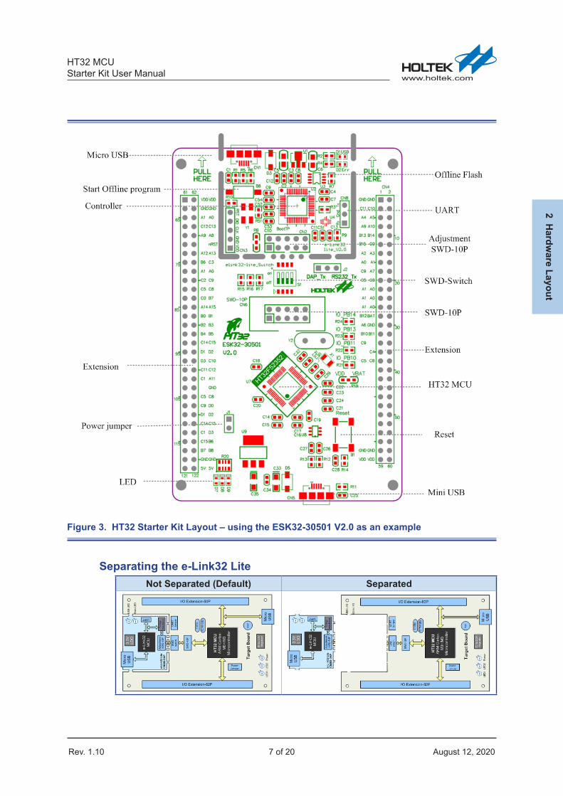
Figure 3. HT32 Starter Kit Layout – using the ESK32-30501 V2.0 as an example
Separating the e-Link32 Lite Not Separated (Default) Separated

Rev. 1.10 8 of 20 August 12, 2020
HT32 MCUStarter Kit User Manual
2 Hardw
are Layout
Serial Wire Debug Interface Switch – S1 S1 Description
Connect the SWD interface between the e-Link32 Lite and the Target MCU – default setting
Disconnect the SWD interface between the e-Link32 Lite and the Target MCU
SWD-10P Connector – CN2, CN6CN2 is the Serial Wire Debug interface connector on the e-Link32 Lite side, while CN6 is on the Target Board side.
Figure 4. SWD-10P Connector
Table 1. SWD-10P ConnectorPin No. Description Pin No. Description
1 VDD 2 SWDIO3 GND 4 SWCLK5 GND 6 NC7 NC 8 NC9 GND 10 Reset

Rev. 1.10 9 of 20 August 12, 2020
HT32 MCUStarter Kit User Manual
2 Hardw
are Layout
2 Hardw
are Layout
e-Link32 Lite Power Option – R8R8 Description
Pin 1 on the CN2 connector on the e-Link32 Lite side is used as the input. The reference voltage is supplied through this pin to the voltage conversion chip – default settingNote that if the e-Link32 Lite has not been separated, the 3.3V on the Target Board will have been connected to CN2-1 through the PCB wire connectionPin 1 on the CN2 connector on the e-Link32 Lite side is used as the output. Here the e-Link32 Lite voltage conversion chip is fixed using 3.3V as the reference voltage. Note that the 3.3V voltage on the Target Board has been connected to CN2-1 through the PCB wire connection, therefore this option is not allowed if the e-Link32 Lite has not been separated
Only the e-Link32 Lite V2.0 version has the R8 option.
e-Link32 Lite Power Option – J8J8 Description
Pin 1 on the CN2 connector on the e-Link32 Lite side is used as the input. The reference voltage is supplied through this pin to the voltage conversion chip – default settingNote that if the e-Link32 Lite has not been separated, the 3.3V on the Target Board will be connected to CN2-1 through the S1 switch and the PCB wire connectionPin 1 of the CN2 connector on the e-Link32 Lite side is used as the output. Here the e-Link32 Lite voltage conversion chip is fixed using the 3.3V as the reference voltageNote that the 3.3V on the Target Board will be connected to CN2-1 through the S1 switch and the PCB wire connection. If the e-Link32 Lite has not been separated, users should switch the S1 to the OFF position to use this option
Only the e-Link32 Lite V2.2 or V2.3 version has the J8 option.
Boot Option – Located on the Board Reverse SideR18 Description
1 or NC – MCU boots from main flash – default setting
0 – MCU boots from bootloader – ISP
High Speed External Crystal Oscillator (HSE) Option R23 & R24 Description
Open, HSE I/O pins disconnected from CN4 – default setting
Short, HSE I/O pins connected to CN4 pins 9 and 10. Y2 must be removed.
The designators on the ESK32-30105 (HT32F12366 SK) are R21 and R22.

Rev. 1.10 10 of 20 August 12, 2020
HT32 MCUStarter Kit User Manual
2 Hardw
are Layout
Low Speed External Crystal Oscillator (LSE) Option R21 & R22 Description
Open, LSE I/O pins disconnected from CN4 – default setting
Short, LSE I/O pins connected to CN4 pins 31 and 32. X1 must be removed.
The designators on the ESK32-30105 (HT32F12366 SK) are R23 and R24.
USB D+/D- OptionR26 & R27 Description
Open, USB D+/D- pins disconnected from the CN4 – default setting
Short, USB D+/D- pins connected to the CN4 pins 55 and 56.
The early Starter Kit board or its Target MCU does not have an integrated USB or its USB D+/D- are not bonded with the GPIO, therefore this option is not available.
MCU Power Jumper – J1J1 Description
The MCU VDD pin is connected to the 3.3V power – default setting
The MCU VDD pin is disconnected from the 3.3V power
The jumper is useful when it is required to measure the MCU power consumption.
UART Option Jumper – J2The Starter Kit arranges a group of the Target MCU UART to be used as external communication interfaces, which can connect to the host computer or other devices. The Target MCU RX pin has the option of connecting to the e-Link32 UART TX pin or to the extension connector, CN4_6: RS232_TX.
J2 Description
The MCU UART RX is connected to the extension connector, CN4_6: RS232_TX – default setting
The MCU UART RX is connected to the e-Link32 UART TX

Rev. 1.10 11 of 20 August 12, 2020
HT32 MCUStarter Kit User Manual
2 Hardw
are Layout
2 Hardw
are Layout
e-Link32 UART Connector – CN8This is the e-Link32 integrated USB to UART function, which is called the “Virtual COM port”, CN8 is the UART side connector.
CN8 Description
Three UART connector pins: Txd, GND and Rxd The e-Link32 will send data on the Txd pin while data will be received on the Rxd pin
Extension Connector CN4-1
Figure 5. Extension Connector 1
Table 2. Extension Connector 1Pin No. Description Pin No. Description
1 GND 2 GND3 I2S_BCLK 4 I2S_WS5 RS232_RX – connect to MCU TX 6 RS232_TX – connect to MCU RX7 M_IO4 8 BUZZER9 M_IO2 10 M_IO311 M_IO0 12 M_IO113 M_TX 14 M_RX15 M_RTS 16 M_CTS17 M_MISO 18 M_CS19 M_SCK 20 M_MOSI21 M_SDA 22 M_SCL23 Touch_SDA 24 Touch_SCL25 EE_SDA 26 EE_SCL27 B0_WAKEUP 28 V_BAT29 VR 30 GND31 LSE_In 32 LSE_Out33 SD_D0/MISO 34 SD_D135 SD_D2 36 SD_D3/CS37 SD_CLK 38 SD_CMD/MOSI39 CSIF_LED 40 SD_CD41 CSIF_SDA 42 CSIF_SCL43 CSIF_RESB 44 CSIF_PWDN45 CSIF_PCLK 46 CSIF_MCLK47 CSIF_HSYNC 48 CSIF_VSYNC

Rev. 1.10 12 of 20 August 12, 2020
HT32 MCUStarter Kit User Manual
2 Hardw
are Layout
Pin No. Description Pin No. Description49 CSIF_D6 50 CSIF_D751 CSIF_D4 52 CSIF_D553 CSIF_D2 54 CSIF_D355 CSIF_D0/USB D- 56 CSIF_D1/USB D+57 GND 58 GND59 3.3V 60 3.3V
Extension connector CN4-2
Figure 6. Extension Connector 2
Table 3. Extension Connector 2Pin No. Description Pin No. Description
61 3.3V 62 3.3V63 GND 64 GND65 I2S_SDA 66 I2S_SCL67 I2S_SDO 68 I2S_SDI69 BOOT1 70 I2S_MCLK71 SWO 72 nRST73 SWCLK 74 SWDIO75 LCD_BL 76 LCD_WE77 LCD_SDA 78 LCD_SCL79 LCD_CS 80 LCD_MISO81 LCD_SCK 82 LCD_MOSI83 LCD_INT 84 LCD_RST85 LCD_AD0 86 LCD_AD187 LCD_AD2 88 LCD_AD389 LCD_AD4 90 LCD_AD591 LCD_AD6 92 LCD_AD793 LCD_AD8 94 LCD_AD995 LCD_AD10 96 LCD_AD1197 LCD_AD12 98 LCD_AD1399 LCD_AD14 100 LCD_AD15
101 LCD_OE 102 LCD_A0103 LCD_TS 104 GND105 Flash_SCK 106 Flash_MOSI107 Flash_MISO 108 Flash_CS
Rev. 1.10 13 of 20 August 12, 2020
HT32 MCUStarter Kit User Manual
2 Hardw
are Layout
2 Hardw
are Layout
Pin No. Description Pin No. Description109 Button1 110 Button2111 LED0 112 LED1113 LED2 114 SCI_CMD115 SCI_RST 116 SCI_CLK117 SCI_DET 118 SCI_DIO119 GND 120 GND121 5V 122 5V
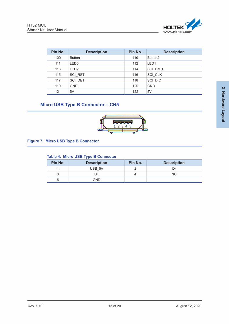
Micro USB Type B Connector – CN5
Figure 7. Micro USB Type B Connector
Table 4. Micro USB Type B ConnectorPin No. Description Pin No. Description
1 USB_5V 2 D-3 D+ 4 NC5 GND

Rev. 1.10 14 of 20 August 12, 2020
HT32 MCUStarter Kit User Manual
3 Connection betw
een the e-Link32 Lite and the Target Board
3 3 Connection between the e-Link32 Lite and the Target Board
e‐Link32 Lite v2.0 Target Board
Figure 8. Connection between the e-Link32 Lite V2.0 and the Target Board
e‐Link32 Lite v2.3 Target Board
Figure 9. Connection between e-Link32 Lite V2.3 and Target Board

Rev. 1.10 15 of 20 August 12, 2020
HT32 MCUStarter Kit User Manual
3 Connection betw
een the e-Link32 Lite and the Target Board
4 Schematics
The diagrams above are the schematic diagram of the connection between the e-Link32 Lite and the Target Board:
▆ The e-Link32 Lite currently uses three hardware versions which are V2.0, V2.2 and V2.3. Because V2.2 and V2.3 are roughly the same, only V2.3 is listed here. The detailed schematic diagram will be attached to the schematic section for reference.
▆ The U4, U5 and U6 level shifter ICs are responsible for converting the SWDIO and SWCLK pin voltage levels to the Target MCU voltage level. When J8 or R8 is selected to be open circuit, CN2-1 is used as an input and the e-Link32 Lite is separated, the reference voltage must be supplied on CN2-1.
▆ J8 or R8 can determine whether VDD_elink32 and CN2-1 are connected together. If they are connected together, the SWDIO and SWCLK pin higher levels are fixed at 3.3V. At the same time CN2-1 has the ability to output 3.3V, which can be supplied to the user’s own board.Here it should be noted that if the user’s own board contains a power supply, then CN2-1 cannot be connected to the user’s own board, otherwise it may cause a power conflict.
▆ CN2 and CN6 are the SWD connectors of the e-Link32 Lite and the Target Board respectively. ● If the e-Link32 Lite is not separated, there is already a PCB line connection on the board, so
switching S1 to the ON position can connect the Target Board without an additional flying line connection.
● If the e-Link32 Lite is not separated and S1 is switched to the OFF position, CN2 can be connected to the user’s own board through a flying line.
● When the e-Link32 Lite is separated, CN2 can be connected to the Target Board CN6 or the user’s own board through a flying line.
▆ The e-Link32 Lite has an integrated USB to UART function which is called the “Virtual COM Port”, CN8 is its UART side connector. ● If the e-Link32 Lite is not separated, users can use the e-Link32 “Virtual COM Port” functions
by connecting J2 to DAP_TX. ● If the e-Link32 Lite is not separated, and users wish to connect the e-Link32 RX to their
board, they need to erase the Target MCU of the Starter Kit to avoid conflict. ● When the e-Link32 Lite is separated, CN8 can be connected to the Target Board or the user’s
own board through a flying line.
4 4 Schematics
This section shows the HT32 MCU Starter Kit circuit diagrams:
▆ e-Link32 Lite V2.0 ▆ e-Link32 Lite V2.2 ▆ e-Link32 Lite V2.3 ▆ HT32F52352 Target Board – ESK32-30501
Other Starter Kit target board circuit diagrams can be downloaded on Holtek official website.

PA01
PA12
PA23
PA34
PA45
PA56
PA67
PA78
VDD33_19
VSS33_110
LDOOUT
13
LDOIN
14
VSS
LDO
15
nRST
16
VBAT
17
PC13_X
TAL3
2KIN
18
PC14_X
TAL3
2KOUT
19
PC15_R
TCOUT
20
PB14_X
TALIN
21
PB15_X
TALO
UT
22
PD1/VDD33_2
23
PD2V
SS33_2
24
PB12/USBDM11
PB13/USBDP12 PA8_BOOT0 25PA9_BOOT1 26PA10 27TRACESWO_PA11 28SWCLK_PA12 29SWDIO_PA13 30PA14 31PA15 32
VDD33_3 35VSS33_3 36
PB0 33PB1 34
PB2
37PB
338
PB4
39PB
540
PB6
41PB
742
PB8
43PB
944
PB10
45PB
1146
VDDA
47VSS
A48
HT32F165x
U2HT32F165x_LQFP48
12345678910
CN2
SWD-10P
VDD_elink32VSS
W_RSTW_SWDIOW_SWCLK
12345
CN3
SW
SWCLK
SWDIO
nRST
R9470
VSS
VSS
VCCB
6VCCA
7
A18
A29
DIR110
DIR2
1
GND 3
B1 5
OE
2
B2 4
U4SN74AVC2T245
SWDIOSWCLK
C13
0.1uF
DC5V
R1 1M
VSS
5V D- D+ ID G
1 2 3 4 5
6
78
9
CN1
USB-Micro
Earth_2 Earth_2
VSS
VSS
R627
C10.1uF
C2
47pF
C347pF
R527
VSS
USBDM_elink
USBDP_elink
D3SS-12W,SS-13W,SS-14W
C122.2uF
C9
0.1uF
XTA
LIN
XTA
LOUT
C10
0.1uF
C11
0.1uF
C7
0.1uF
VSS
VSS
LED1
LED2
LED3
VDD_elin
k32
W_R
ST
W_SWDIOW_SWCLK
SWDIO
SWCLK
USBDM_elinkUSBDP_elink
DIR1
DIR2
MOSI
MISOSCK
DIR1
DIR2
MOSIMISO
SCK
nRST
C540.01uF
R10100k
W_RST
Flash_CS
Flash_MISOFlash_MOSIFlash_SCK
nRST
VDD_elink32
VDD_elink32
VDD_elink32
VDD_elink32
VDD_TargetBoard
VDD_elink32
VDD_elink32
VDD_elink32
C510UF
C610UF
PA9_BOOT1
VDD_elink32
XTA
LIN
XTA
LOUT
R3
10kVDD_elink32
DAP_
TXDAP_
RX
DAP_TX
DAP_RX
C8
0.1uF
1 2 3 4
U1HT7833
VSS
VSS
R51 1M (NC)
Y1 8M (NC)
C5210pF (NC)
C5310pF (NC)
CS1
SO2
WP3
GND4 SI 5SCLK 6HOLD 7VCC 8
U3MX25L8006E (NC)
FLASHC40.1uF (NC)
R710k (NC)
Flash_CSFlash_MISO
Flash_MOSIFlash_SCK
B8
IAP (NC)PA10_IAP
VDD_elink32
VDD_elink32
VDD_elink32SWO
SWO SWO
R8 0 (NC)
iBOOT1_TestPoint
Short BOOT1 to GND and Reset MCU, can boot to Bootloader
VSS
C51
0.1uF
VDD_TargetBoard
0
VCCB
R9:The Level Shift VCCB Power SelectionDefault Use TargetBoard Power
Don't configure PD1/PD2 as Output or Enable Internal Pull Resistor
123
CN8
Virtual COM Port
Designator Reserved For Target Board as below, Do NOT UseB1 to B7C14 to C50CN4 to CN7D5 to D50J1 to J7R11 to R50 S1 to S7U7 to U20X1Y2
Green
D1 USB
Red
D2 Err VDD_elink32
LED1
LED2
R2 330
R4 330
DAP_TX
DAP_RX
GND VSS
VDD_TargetBoard VDD33
Figure 10. e-Link32 Lite V2.0

PA01
PA12
PA23
PA34
PA45
PA56
PA67
PA78
VDD33_19
VSS33_110
LDOOUT
13
LDOIN
14
VSS
LDO
15
nRST
16
VBAT
17
PC13
_XTA
L32K
IN18
PC14
_XTA
L32K
OUT
19
PC15
_RTC
OUT
20
PB14
_XTA
LIN
21
PB15
_XTA
LOUT
22
PD1/VDD33
_223
PD2V
SS33_2
24
PB12/USBDM11
PB13/USBDP12 PA8_BOOT0 25PA9_BOOT1 26PA10 27TRACESWO_PA11 28SWCLK_PA12 29SWDIO_PA13 30PA14 31PA15 32
VDD33_3 35VSS33_3 36
PB0 33PB1 34
PB2
37PB
338
PB4
39PB
540
PB6
41PB
742
PB8
43PB
944
PB10
45PB
1146
VDDA
47VSS
A48
HT32F165x
U2HT32F165x_LQFP48
VDD_elink32VSS
W_RSTW_SWDIOW_SWCLK
12345
CN3
SW(NC)
DC5V
R1 1M
VSS
5V D- D+ ID G
1 2 3 4 5
6
78
9
CN1
USB-Micro
Earth_2 Earth_2
VSS
VSS
R627
C10.1uF
C2
47pF
C347pF
R527
VSS
USBDM_elink
USBDP_elink
D3SS-12W,SS-13W,SS-14W
C122.2uF
C9
0.1uF
XTA
LIN
XTA
LOUT
C10
0.1uF
C11
0.1uF
C7
0.1uF
VSS
VSS
LED1
LED2
LED3
VDD_elin
k32
W_R
ST
W_SWDIOW_SWCLK
USBDM_elinkUSBDP_elink
MOSI
DIR
1DIR
2
MOSIMISO
SCK
nRST
C540.01uF
R10100k
W_RST
Flash_CS
Flash_MISOFlash_MOSIFlash_SCK
VDD_elink32
VDD_elink32
VDD_elink32
VDD_elink32
VDD_elink32
VDD_elink32
VDD_elink32
C510UF
C610UF
PA9_BOOT1
R3
10kVDD_elink32
DAP_
TXDAP_
RX
C8
0.1uF
1 2 3 4
U1HT7833
VSS
CS1
SO2
WP3
GND4 SI 5SCLK 6HOLD 7VCC 8
U3MX25L8006E (NC)
FLASHC40.1uF (NC)
R710k (NC)
Flash_CSFlash_MISO
Flash_MOSIFlash_SCK
B8
IAP (NC)PA10_IAP
VDD_elink32
VDD_elink32
VDD_elink32SWO
iBOOT1_TestPoint
Short BOOT1 to GND and Reset MCU, can boot to Bootloader
VSS
Don't configure PD1/PD2 as Output or Enable Internal Pull Resistor
Designator Reserved For Target Board as below, Do NOT UseB8C4 C52 C53CN2 CN3R7 R51U3Y1
Green
D1 USB
Red
D2 Err VDD_elink32
LED1
LED2
R2 330
R4 330
GND VSS
C13 0.1uF
VDD_elink32
C51
0.1uF
VDD_TargetBoard
VCCA1
GND2
A3 B 4DIR 5VCCB 6U5
SN74LVC1T45
VCCA1
GND2
A3 B 4DIR 5VCCB 6U6
SN74LVC1T45
DIR2
DIR1
R9 470
MOSI MISOVSS
VSS
VDD_elink32
VCCB
SCK SWCLK
SWDIO
VCCB
1 2 3 4 5 6 7 8 9 10
CN2 SWD-10P(NC)
SWCLK
SWDIO
nRST
SWDIO
SWCLK
nRST
VDD_TargetBoard
DAP_TX
DAP_RX
SWO
VDD_TargetBoard
1 2 3
CN8
Virtual COM Port
DAP_TX
DAP_RX
1 R15 100
1 R16 100
1 R17 100
J8: VDD OptionShort : OutputOpen: Input
VDD_TargetBoardVDD_elink32J8
VDD_TargetBoard
Figure 11. e-Link32 Lite V2.2

USBDM_elinkUSBDP_elink
0805-C
C510uF
HT_SOT-89
VIN2
GND
1
VOUT 34
U1HT7833
GND
0805-C
C610uF
VDD_elink32DC5V
SMA
D3SS-14
0603
-RR6
2706
03-R
R5
27 0603-C
C247pF
0603-C
C347pF
5V D- D+ ID G
1 2 3 4 5
679
8
USB-Micro
CN1USB-Micro
Earth_2Earth_2
0603-RR1 1M
0603-C
C10.1uF GND
GND
USB Port
Power
FLASH
CS1
SO2
WP3
GND4 SI 5SCLK 6HOLD 7VCC 8
USON_4x4
U3MX25L8006E (NC)
0603-R
R710K(NC)
Flash_CSFlash_MISO
VDD_elink32
GND
0603-CC4 0.1uF(NC)
VDD_elink32
VDD_elink32
GND
Flash_MOSIFlash_SCK
GND
KEY2-SMT
B8
IAP(NC)PA10_IAP
Reserved don't fit the component
DAP_TXDAP_RX
DAP_TXDAP_RX
1 2 3
HDR1X3
CN8Virtual COM Port
0603-RR51 100
GND
LED1
LED2
GreenLED_0603
D1 USB
RedLED_0603
D2 Err
VDD_elink32
0603-R
R2
330
0603-R
R4
330
LEDs
VCCA1
GND2
A3 B 4DIR 5VCCB 6
SOT23-6
U6
SN74LVC1T45
VDD_elink32
SCK SWCLKDIR2
VDD_TargetBoard
GND
GNDVCCA1
GND2
A3 B 4DIR 5VCCB 6
SOT23-6
U5
SN74LVC1T45
MISO
0603-R
R9470
MOSI
VDD_elink32
0603-C
C130.1uF
0603-C
C510.1uF GND
VDD_TargetBoard
DIR1SWDIO
HDR1X2J8VDD_elink32 VDD_TargetBoard
J8: VDD OptionShort : OutputOpen: Input
Level Shift
UART Interface
Designator Reserved For Target Board as below, Do NOT Use in this sheet:
B1 to B7C14 to C50CN4 to CN7D5 to D50J1 to J7R11 to R50 S1 to S7U7 to U20X1 , Y2
Note
W_RSTW_SWDIOW_SWCLK
GND
LED1
LED2
LED3
W_RST
W_SWDIOW_SWCLK
USBDM_elinkUSBDP_elink
DIR1
DIR2
MOSIMISO
SCK
nRST
Flash_CS
Flash_MISOFlash_MOSIFlash_SCK
VDD_elink32
VDD_elink32
PA9_BOOT
DAP_
TXDAP_
RX
PA10_IAP
SWO
0603-C
C90.1uF
0603-C
C70.1uF
0603-C
C80.1uF
0603-R
R10100K
0603-C
C540.01uF
GND
VDD_elink32
PA01
PA12
PA23
PA34
PA45
PA56
PA67
PA78
PC49
PC510
CLD
O13
VDD_1
14
VSS
_115
nRST
16
PB9
17
X32
KIN
/PB10
18
X32
KOUT/PB
1119
RTC
OUT/PB
1220
XTA
LIN/PB13
21
XTA
LOUT/PB
1422
PB15
23
PC0
24
USBDM11
USBDP12 PA8 25PA9_BOOT 26PA10 27PA11 28PA12/SWCLK 29PA13/SWDIO 30PA14 31PA15 32
VDD_2 35VSS_2 36
PB0 33PB1 34
PB2
37PB
338
PB4
39PB
540
PC1
41PC
242
PC3
43PB
644
PB7
45PB
846
VDDA
47VSS
A48
HT32F52341
HT_LQFP48_7*7
U2HT32F52341_LQFP48
VDD_elink32
0603-R
R3
10KVDD_elink32
0603-C
C122.2uF
TP_59
TP1
BOOT
GND
GND
12345
HDR1X5
CN3
e-Link32 SWD (NC)
GND
VDD_elink32
MCU
SWCLK
SWDIO
nRST
SWDIO
SWCLK
nRST
VDD_TargetBoard
SWO
VDD
1
SWDIO
2
GND
3
SWCLK
4
GND
5
SWO
6
NC
7
NC
8
GND
9
nRST
10
DIP-SWD-10P-2
CN2SWD-10P (NC)
0603-RR52 100
0603-RR53 100
GND
SWD Interface
0603-RR54 100
0603-RR55 100
0603-RR56 100
Figure 12. e-Link32 Lite V2.3

C280.01uF
F_NRS
T
R14100K
GND
VDD33
VDD33
1 2Y2
8MHzC3112pF
C3212pF
C142.2uF
MVDD
MVDD
MVDD
GND
GND
C222.2uF
C21 2.2uF
C24 0.1uF(can be removed)
C230.1uF
GND
MVDD
VBA
T
C19
0.1uF
C20
0.1uF
C18
0.1uF
MVDD
C2920pF
C3020pF
C150.1uF
PB10_L
SEi
PB11_L
SEo
F_NRST
USBDM_PC6USBDP_PC7
MVDD
GND
PA0_RTS/I2CPA1_CTS/I2C
PA2PA3PA4PA5PA6PA7
PC9
PC10
PC11
PC12
PB15
WAK_PB1
2PD
0
PD1PD2PD3
PC1_LE
D/OE
PC2
PC3
PC13PA8PA9_BOOT1/MPA10PA11PA12PA13PA14PA15
PB0PB1
PC4PC5
PB2
PB3
PB4
PB5
PC8
PC14
PC15_L
ED/SCI
PB6_LC
D/SCI
PB8
VSSVSSDC5V DC5V
VSSVSSVDD33VDD33
VDD33VDD33 VSS
PB13/HSEi PB14/HSEo
PB13 PB14
PB13/HSE
iPB
14/HSE
o
R184.7k(NC)
PA9_BOOT1/MD8 LED2
D9 Power
D7 LED1
R4B 5
R1B 8R2B 7R1A1
R3B 6R3A3 R2A2
R4A4
R20
R8P4R_330
VDD33
DC5V
USB Port & PowerR11 1M
C3510uF/CASEA
VSS
5V D- D+ ID G
1 2 3 4 5
678
9
CN5
USB-Micro
Earth_1 Earth_1
VSS
VSS
R1327
C250.1uF
C26
47pF
C340.1uF
VDD33
J1 MVDD
C2747pF
R1227
C3310uF/CASEA
VSS
D5
SS-12W,SS-13W,SS-14W
Boot pinLSE/HSE/BAT Jumper
B1Reset
X1
32768
PB10 PB11
12345678910
CN6
SWD-10PVDD33
PA12
PA13
F_NRST
PA12PA13 SWDIO
SWCLKF_NRST nRST
USBDP_PC7
PA0_RTS/I2CPA1_CTS/I2C
PA2 PA3
PA4
PA6
PA7
PC9PC4
PC5 PC8
USBDM_PC6
PA0_RTS/I2C PA1_CTS/I2C
GND GND
PA0_RTS/I2CPA1_CTS/I2C
PA0_RTS/I2CPA1_CTS/I2C PC9PC5 PC8
PC9PC5 PC8
PC10PC11
PC12
WAK_PB12
PD0
PB13 PB14
PB10 PB11
V_BAT
GND
GND
PB15 PC0_LCD/M
PC0_LCD/M
GND
PD1 PD2
PC13PA8
PA9_BOOT1/M PA10
PA11
PA12 PA13
PA14 PA15PB0 PB1
F_NRST
PC1_LED/OE
PC2
PC3
PB2 PB3PB4 PB5
PC14 PC15_LED/SCI
PB6_LCD/SCIPB7_LCD/SCI PB8
PA9_BOOT1/M
4.7k(NC)
PB6_LCD/SCI
PD3PC15_LED/SCI
PC1_LED/OE
PC10PC11 PC12
PD1 PD2PD3
PC14 PC15_LED/SCI
PB7_LCD/SCI
PB7_LC
D/SCI
USBDP_PC7 USBDM_PC6
VSSDC5V
PC14PC15_LED/SCI
R210(NC)
R220(NC)
R230(NC)
R240(NC)VBAT
V_BAT
R190
MVDD
NC
PB13/HSE
i
PB14/HSE
o
PB10_LSEi PB11_LSEo
PB10_L
SEi
PB11_L
SEo
PC9PC5 PC8
PC0_LC
D/M
GND1 GND 2
I2S_BCLK3 I2S_WS 4
RS232_RX5 RS232_TX 6
M_IO47
B0_WAKEUP27
M_IO29 M_IO3 10
M_IO011 M_IO1 12
M_TX13 M_RX 14
M_RTS15 M_CTS 16
M_MISO17 M_CS 18
M_SCK19 M_MOSI 20
M_SDA21 M_SCL 22
Touch_SDA23 Touch_SCL 24
EE_SDA25 EE_SCL 26
BUZZER 8
V_BAT 28
VR29 GND 30
SD_D0/MISO33 SD_D1 34
SD_D235 SD_D3/CS 36
SD_CLK37 SD_CMD/MOSI 38
CSIF_LED39 SD_CD 40
CSIF_RESB43 CSIF_PWDN 44
CSIF_MCLK 46CSIF_PCLK45
CSIF_VSYNC 48CSIF_HSYNC47
CSIF_D649 CSIF_D7 50
CSIF_D451 CSIF_D5 52
CSIF_D253 CSIF_D3 54
CSIF_D055 CSIF_D1 56
GND57 GND 58
3.3V59 3.3V 60
3.3V61 3.3V 62
GND63 GND 64
I2S_SDO67 I2S_SDI 68
BOOT169 I2S_MCLK 70
SWDIO 74SWCLK73
LCD_BL75 LCD_WE 76
LCD_SDA77 LCD_SCL 78
LCD_CS79 LCD_MISO 80
LCD_SCK81 LCD_MOSI 82
LCD_INT83 LCD_RST 84
LCD_AD085 LCD_AD1 86
LCD_AD287 LCD_AD3 88
LCD_AD489 LCD_AD5 90
LCD_AD691 LCD_AD7 92
LCD_AD893 LCD_AD9 94
LCD_AD1095 LCD_AD11 96
LCD_AD1297 LCD_AD13 98
LCD_AD1499 LCD_AD15 100
LCD_OE101 LCD_A0 102
LCD_TS103 GND 104
Flash_SCK105 Flash_MOSI 106
Flash_MISO107 Flash_CS 108
Button1109 Button2 110
LED0111 LED1 112
LED2113 SCI_CMD 114
SCI_RST115 SCI_CLK 116
SCI_DET117 SCI_DIO 118
GND119 GND 120
5V121 5V 122
CSIF_SDA41 CSIF_SCL 42
nRST 72SWO71
LSE_In31 LSE_Out 32
I2S_SDA65 I2S_SCL 66
CN4
GPDVB_Connector_S
C16 10pF(NC)
C17 10p(NC)
R15 100
R16 100
R17 100
GND VSS
PA01PA12PA23PA34PA45PA56PA67PA78VDD33_19VSS33_110PC411PC512
LDOOUT
17LD
OIN
18VSS
LDO
19nR
ST20
VBA
T21
PB10_X
TAL3
2KIN
22PB
11_X
TAL3
2KOUT
23PB
12_R
TCOUT
24
PB13_X
TALIN
26PB
14_X
TALO
UT
27PB
1528
PC0
29
PC813PC914PC6/USBDM15PC7/USBDP16
PD0
25
PC10
30PC
1131
PC12
32
PC13 33PA8 34PA9_BOOT 35PA10 36PA11 37SWCLK_PA12 38SWDIO_PA13 39PA14 40PA15 41VDD33_3 42VSS33_3 43PB0 44PB1 45PD1 46PD2 47PD3 48
PB2
49PB
350
PB4
51PB
552
PC14
53PC
1554
VDD33_4
55VSS
33_4
56PC
157
PC2
58PC
359
PB6
60PB
761
PB8
62VDDA
63VSS
A64
HT32F52352
U7HT32F52352_LQFP64
I/O11GND2I/O23 I/O3 4VCC 5I/O4 6
U8
TESDS5V0A
32
1
4
VinVout
GND
TABLM1117
U9
LM1117
1234
8765
S1
SW DIP-4
DAP_TX
DAP_RX
12
3J2
JUMPER2
PA5RS232_TX
RS232_TX
1uF (or 2.2uF) capacitor fromthe LDOOUT/CLDO to the VSS isrequired (close to MCU).
External pull up resistance of the nRST canbe changed to 10K for interference/noiserejection. The capacitor from the nRST toVSS can be NC if no button used.
The VBAT must connect to the VDDwhen no extra battery is used in thesystem (VBAT floating is not allowed). The BOOT pin must be maintained at high level when reset.
4.7K external pull up resistance may be required for the BOOTpin (for interference/noise rejection and rising time during thereset).
Figure 13. HT32F52352 Target Board – ESK32-30501

Rev. 1.10 20 of 20 August 12, 2020
HT32 MCUStarter Kit User Manual
4 Schematics
Copyright© 2020 by HOLTEK SEMICONDUCTOR INC.
The information appearing in this Data Sheet is believed to be accurate at the time of publication. However, Holtek assumes no responsibility arising from the use of the specifications described. The applications mentioned herein are used solely for the purpose of illustration and Holtek makes no warranty or representation that such applications will be suitable without further modification, nor recommends the use of its products for application that may present a risk to human life due to malfunction or otherwise. Holtek's products are not authorized for use as critical components in life support devices or systems. Holtek reserves the right to alter its products without prior notification. For the most up-to-date information, please visit our web site at http://www.holtek.com.