HS-874P - COMMELL
58
HS-874P Half-size PISA CPU Card User’s Manual Edition: 1.1 2009/05/08
Transcript of HS-874P - COMMELL

HS-874P
Half-size PISA CPU Card
User’s Manual
Edition: 1.1 2009/05/08

HS-874P User’s Manual
2
Copyright
Copyright 2008. All rights reserved. This document is copyrighted and all rights are reserved. The information in this document is subject to change without prior notice to make improvements to the products. This document contains proprietary information and protected by copyright. No part of this document may be reproduced, copied, or translated in any form or any means without prior written permission of the manufacturer. All trademarks and/or registered trademarks contains in this document are property of their respective owners.
Disclaimer
The company shall not be liable for any incidental or consequential damages resulting from the performance or use of this product. The company does not issue a warranty of any kind, express or implied, including without limitation implied warranties of merchantability or fitness for a particular purpose. The company has the right to revise the manual or include changes in the specifications of the product described within it at any time without notice and without obligation to notify any person of such revision or changes.
Trademark
All trademarks are the property of their respective holders.
Any questions please visit our website at TUhttp://www.commell.com.twUT.
HS-874P User’s Manual
3
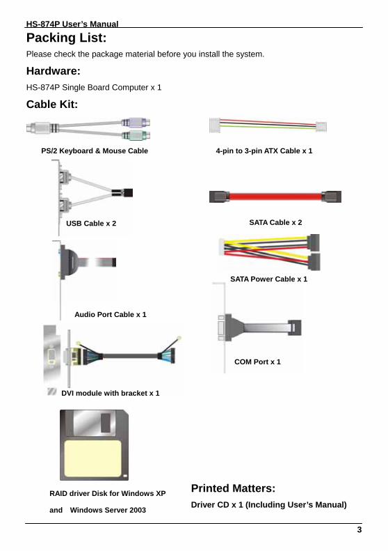
Packing List: Please check the package material before you install the system.
Hardware: HS-874P Single Board Computer x 1
Cable Kit:
4-pin to 3-pin ATX Cable x 1
USB Cable x 2
Printed Matters: Driver CD x 1 (Including User’s Manual)
SATA Cable x 2
RAID driver Disk for Windows XP
and Windows Server 2003
PS/2 Keyboard & Mouse Cable
SATA Power Cable x 1
Audio Port Cable x 1
DVI module with bracket x 1
COM Port x 1
HS-874P User’s Manual
4
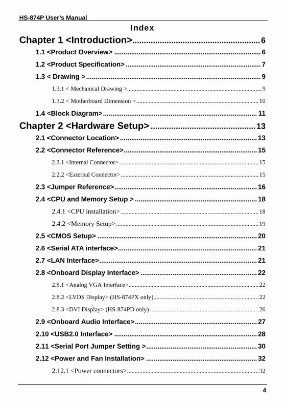
Index Chapter 1 <Introduction>........................................................6
1.1 <Product Overview> .............................................................................. 6 1.2 <Product Specification> ........................................................................ 7 1.3 < Drawing > ............................................................................................. 9
1.3.1 < Mechanical Drawing >.......................................................................................9 1.3.2 < Motherboard Dimension >............................................................................... 10
1.4 <Block Diagram>.................................................................................. 11 Chapter 2 <Hardware Setup> ..............................................13
2.1 <Connector Location> ......................................................................... 13 2.2 <Connector Reference>....................................................................... 15
2.2.1 <Internal Connector> .......................................................................................... 15 2.2.2 <External Connector>......................................................................................... 15
2.3 <Jumper Reference>............................................................................ 16 2.4 <CPU and Memory Setup > ................................................................. 18
2.4.1 <CPU installation> ......................................................................................... 18 2.4.2 <Memory Setup>............................................................................................ 19
2.5 <CMOS Setup> ..................................................................................... 20 2.6 <Serial ATA interface>.......................................................................... 21 2.7 <LAN Interface>.................................................................................... 21 2.8 <Onboard Display Interface> .............................................................. 22
2.8.1 <Analog VGA Interface>.................................................................................... 22 2.8.2 <LVDS Display> (HS-874PX only).................................................................... 22 2.8.3 <DVI Display> (HS-874PD only) ...................................................................... 26
2.9 <Onboard Audio Interface>................................................................. 27 2.10 <USB2.0 Interface> ............................................................................ 28 2.11 <Serial Port Jumper Setting >........................................................... 30 2.12 <Power and Fan Installation> ........................................................... 32
2.12.1 <Power connectors>..................................................................................... 32

HS-874P User’s Manual
5
2.12.2 <Fan Connectors> ........................................................................................ 33 2.13 <GPIO Interface> ................................................................................ 34 2.14 <Switch and Indicator>...................................................................... 35
Chapter 3 <System Configuration>...................................37 3.1 <SATA configuration>.......................................................................... 37 3.2 <SATA RAID Configuration> ............................................................... 38 3.3 <Audio Configuration> ........................................................................ 42 3.4 <Video Memory Setup>........................................................................ 43
Chapter 4 <BIOS Setup>.......................................................45 Appendix A <I/O Port Pin Assignment>...........................47
A.1 <Serial ATA Port>................................................................................. 47 A.2 <Serial Port>......................................................................................... 47 A.3 <VGA Port> ...................................................................................... 47 A.4 <LAN Port> ........................................................................................... 48 A.5 <AT Keyboard Port> ............................................................................ 48 A.6 <PS/2 Keyboard & Mouse Port>......................................................... 48
Appendix B <Flash BIOS>....................................................50 B.1 <BIOS Auto Flash Tool>...................................................................... 50 B.2 <Flash Method> ................................................................................... 50
Appendix C <System Resources>.....................................51 C.1 <I/O Port Address Map>...................................................................... 51 C.2 <Memory Address Map> ..................................................................... 53 C.3 <System IRQ Resources>................................................................... 54
Appendix D <Programming GPIO’s>................................55 Appendix E <Watch Dog timer Setting >.........................56

HS-874P User’s Manual Introduction
Product Overview 6
Chapter 1 <Introduction> 1.1 <Product Overview> The HS-874P is an all-in-one single board computer with PISA bus supporting Intel Core2
Quad/ Core 2 Duo processor for 800/1066/1333 MHz front side bus, Intel Q35 and ICH9DO
chipset, integrated GMA3100 graphics, DDR2 SO-DIMM memory, Realtek ALC888 HD
Audio, Serial ATA and one Intel 82573L Gigabit LAN.
Intel LGA775 Processor
The board supports Intel Core 2 Quad/ Core 2 Duo processor with 800/1066/1333 MHz
front side bus, 8MB L2 cache, to provide more powerful performance than before.
New features for Intel Q35 chipset
The board integrates Intel Q35 and ICH9DO chipset, to provide new supports Intel
GMA3100 graphics, DDR2 667/800 memory, built-in high speed mass storage interface of
serial ATA, HD Audio with 2 channels surrounding sound.
All in One multimedia solution
Based on Intel Q35 and ICH9DO chipset, the board provides high performance onboard
graphics, 24-bit Dual channel LVDS interface or DVI and 2 channels HD Audio to meet the
every requirement of the multimedia application.
HS-874P User’s Manual Introduction
Product Specification 7
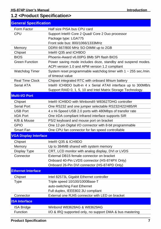
1.2 <Product Specification> General Specification
Form Factor Half size PISA bus CPU card CPU Support Intel® Core 2 Quad/ Core 2 Duo processor
Package type: LGA775 Front side bus: 800/1066/1333MHz
Memory DDRII 667/800 MHz SO-DIMM up to 2GB Chipset Intel® Q35 and ICH9DO BIOS Phoenix-Award v6.00PG 8Mb SPI flash BIOS Green Function Power saving mode includes doze, standby and suspend modes.
ACPI version 1.0 and APM version 1.2 compliant Watchdog Timer System reset programmable watchdog timer with 1 ~ 255 sec./min.
of timeout value Real Time Clock Chipset integrated RTC with onboard lithium battery Serial ATA Intel® ICH9DO built-in 4 x Serial ATAII interface up to 300MB/s
Support RAID 0, 1, 5, 10 and Intel Matrix Storage Technology. Multi-I/O Port
Chipset Intel® ICH9DO with Winbond® W83627DHG controller Serial Port One RS232 and one jumper selectable RS232/422/485/IR USB Port 4 x Hi-Speed USB 2.0 ports with 480Mbps of transfer rate IrDA Port One IrDA compliant Infrared interface supports SIR K/B & Mouse PS/2 keyboard and mouse port on bracket GPIO One 12-pin Digital I/O connector with 8-bit programmable Smart Fan One CPU fan connector for fan speed controllable
VGA Display Interface Chipset Intel® Q35 & ICH9DO Memory Up to 384MB shared with system memory Display Type CRT, LCD monitor with analog display, DVI or LVDS Connector External DB15 female connector on bracket
Onboard 40-Pin LVDS connector (HS-874PX Only) Onboard 26-Pin DVI connector (HS-874PD Only)
Ethernet Interface Chipset Intel 82573L Gigabit Ethernet controller Type Triple speed 10/100/1000Base-T
auto-switching Fast Ethernet Full duplex, IEEE802.3U compliant
Connector External one RJ45 connector with LED on bracket ISA Interface
ISA Bridge Winbond W83628AG & W83629AG Function I/O & IRQ supported only, no support DMA & bus mastering
HS-874P User’s Manual Introduction
Product Specification 8
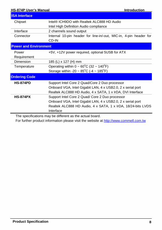
ISA Interface
Chipset Intel® ICH9DO with Realtek ALC888 HD Audio Intel High Definition Audio compliance
Interface 2 channels sound output Connector Internal 10-pin header for line-in/-out, MIC-in, 4-pin header for
CD-IN Power and Environment
Power Requirement
+5V, +12V power required, optional 5USB for ATX
Dimension 185 (L) x 127 (H) mm Temperature Operating within 0 ~ 60 P
oPC (32 ~ 140P
oPF)
Storage within -20 ~ 85P
oPC (-4 ~ 185P
oPF)
Ordering Code HS-874PD Support Intel Core 2 Quad/Core 2 Duo processor
Onboard VGA, Intel Gigabit LAN, 4 x USB2.0, 2 x serial port Realtek ALC888 HD Audio, 4 x SATA, 1 x IrDA, DVI Interface
HS-874PX Support Intel Core 2 Quad/ Core 2 Duo processor Onboard VGA, Intel Gigabit LAN, 4 x USB2.0, 2 x serial port Realtek ALC888 HD Audio, 4 x SATA, 1 x IrDA, 18/24-bits LVDS Interface
The specifications may be different as the actual board. For further product information please visit the website at TUhttp://www.commell.com.twUT

HS-874P User’s Manual Introduction
Mechanical Drawing 9
1.3 < Drawing > 1.3.1 < Mechanical Drawing >
Inch

HS-874P User’s Manual Introduction
Block Diagram 10
127 mm
28.6 mm
185 mm
1.3.2 < Motherboard Dimension >
HS-874P User’s Manual Introduction
Mechanical Drawing 11
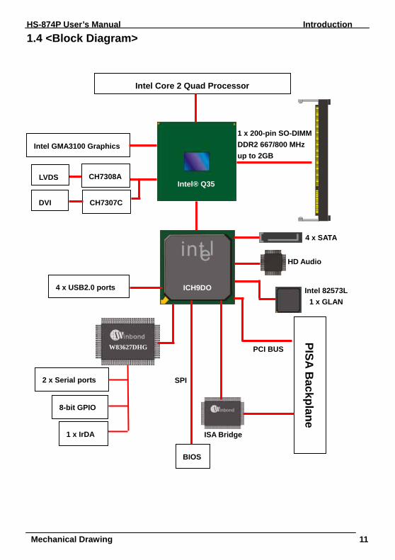
1.4 <Block Diagram>
Intel Core 2 Quad Processor
Intel GMA3100 Graphics
Intel® Q35
ICH9DO
HD Audio
W83627DHG
4 x SATA
2 x Serial ports
4 x USB2.0 ports
8-bit GPIO
Intel 82573L 1 x GLAN
1 x 200-pin SO-DIMM DDR2 667/800 MHz up to 2GB
1 x IrDA
PISA Backplane
ISA Bridge
CH7308ALVDS
CH7307CDVI
PCI BUS
BIOS
SPI
HS-874P User’s Manual
12
(This Page is Left for Blank)
HS-874P User’s Manual Hardware Setup
Connector Location 13
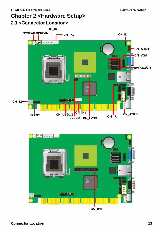
Chapter 2 <Hardware Setup> 2.1 <Connector Location>
CPUFAN
JFRNT JVLCD
CN 12V
CN_IN
SATA1/2/3/4
SYSFAN
CN_LVDSCN_USB1/2 CN_IR
CN_INV CN_ATKB
CN_VGA
CN_AUDIO
CN_DVI
DC_IN
CN_PS

HS-874P User’s Manual Hardware Setup
Connector Location 14
PS2 COM1 RJ45 CRT
SO-DIMM

HS-874P User’s Manual Hardware Setup
Connector Reference 15
2.2 <Connector Reference> 2.2.1 <Internal Connector>
Connector Function Remark DIMM 200-pin DDR2 SDRAM SO-DIMM slot Standard S_ATA1/2/3/4 7-pin Serial ATA connector Standard DC_IN 4-pin AT power supply connector Standard CN_12V 4-pin +12V additional power supply connector Standard CN_PS 3-pin ATX function connector Standard CN_AUDIO 5 x 2-pin audio connector Standard CDIN 4-pin CD-ROM audio input connector Standard CN_DIO 6 x 2-pin digital I/O connector Standard CN_LVDS 20 x 2-pin LVDS connector (HS-874PX) CN_INV 5-pin LCD inverter connector (HS-874PX) CN_USB1/2 5 x 2-pin USB connector Standard CPUFAN 4-pin CPU cooler fan connector Standard SYSFAN 3-pin system cooler fan connector Standard CN_IR 5-pin IrDA connector Standard CN_ATKB 5-pin AT keyboard connector Standard CN_DVI 26-pin DVI connector (HS-874PD) JFRNT 14-pin front panel switch/indicator connector Standard CN_COM2 10-pin serial port connector Standard CN_VGA 8 X 2 pin VGA connector (pitch=2.0mm) Standard
2.2.2 <External Connector>
Connector Function Remark CRT DB15 VGA connector Standard RJ45 One RJ45 LAN connector Standard COM1 Serial port connector Standard PS2 PS/2 keyboard and mouse connector Standard

HS-874P User’s Manual Hardware Setup
Jumper Reference 16
2.3 <Jumper Reference> Jumper Function JRTC CMOS Operating/Clear Setting JVLCD LCD Panel Voltage Setting JCSEL1/2 COM2 RS232/422/485/IR mode setting JP1/JP2 COM PORT Voltage support
JVLCD
JRTC
JCSEL1
JCSEL2
JP2/JP1

HS-874P User’s Manual Hardware Setup
CPU installation 17
Jumper: JP1 (COM 1) Type: onboard 3 x 2-pin header
JP1 Mode 1-3 Pin1 with +5V power. 2-4 Pin9 with +12V power. 3-5 Pin1 with DCD signal 4-6 Pin9 with RI signal
Default setting
Jumper: JP2 (COM 2) Type: onboard 3 x 2-pin header
JP2 Mode 1-3 Pin1 with +5V power. 2-4 Pin9 with +12V power. 3-5 Pin1 with DCD/ 422TX-/485- signal 4-6 Pin9 with RI signal
Default setting
6 5 6 5
2 1 2 1
JP2 JP1

HS-874P User’s Manual Hardware Setup
CPU Installation 18
2.4 <CPU and Memory Setup > 2.4.1 <CPU installation>
HS-874P has a LGA775 CPU socket onboard; please check following steps to install the
processor properly.
Attention If HS-874P needs RMA please Keep CPU socket cover on the CPU Socket.
Warring If CPU Socket internal Pin damage We could not provide warranty.
Intel® Core 2 Duo /Quad processor Package type: 775 pin PLGA L2 Cache: 8 MB FSB: 800/1066/1333MHz (266MHz x 4)Manufacturing: 65nm, 45nm Intel Hyper Threading Technology and Core 2 Duo /Quad supported
1. Lift this bar
2. Uncover this plate
Check point
3. Place the CPU on the top ofthe pins
3. Cover this plate 4. Lock this bar
Notice: Please place the CPU on the pins tenderly to avoid bending the pins

HS-874P User’s Manual Hardware Setup
Memory Setup 19
2.4.2 <Memory Setup>
HS-874P has one 200-pin DDR2 SO-DIMM support up to 2GB of memory capacity. The
memory frequency supports 667/800 MHz. Only Non-ECC memory is supported.
SO-DIMM

HS-874P User’s Manual Hardware Setup
CMOS Setup 20
2.5 <CMOS Setup> The board’s data of CMOS can be setting in BIOS. If the board refuses to boot due to inappropriate CMOS settings, here is how to proceed to clear (reset) the CMOS to its default values. Jumper: JRTC
Type: Onboard 3-pin jumper JRTC Mode 1-2 Clear CMOS 2-3 Normal Operation
Default setting
JRTC
1 3

HS-874P User’s Manual Hardware Setup
Serial ATA Interface 21
2.6 <Serial ATA interface> Based on Intel ICH9DO, the board provides four Serial ATA interfaces with up to 300MB/s of
transfer rate.
2.7 <LAN Interface> The Intel 82573L supports triple speed of 10/100/1000Base-T, with IEEE802.3 compliance
and Wake-On-LAN supported.
SATA1/2/3/4
LAN

HS-874P User’s Manual Hardware Setup
Digital Display 22
2.8 <Onboard Display Interface> Based on Intel Q35 chipset with built-in GMA (Graphic Media Accelerator) 3100 graphics,
the board provides one DB15 connector on real external I/O port, and one 40-pin LVDS
interface with 5-pin LCD backlight inverter connector. The board provides dual display
function with clone mode and extended desktop mode for CRT and LCD or DVI.
2.8.1 <Analog VGA Interface>
Please connect your CRT or LCD monitor with DB15 male connector to the onboard DB15
female connector on rear I/O port.
2.8.2 <LVDS Display> (HS-874PX only)
The board provides one 40-pin LVDS connector for 18/24-bit dual channel panels, supports
up to 1600 x 1200 (UXGA) of resolution, with one LCD backlight inverter connector and one
jumper for panel voltage setting.
Effective patterns of connection: 1-2 / 3-4 / 5-6
Warning: others cause damages
VGA
CN_LVDS 2 40
1 39 CN_INV
1 5JVLCD
3
4 5
6
2
1

HS-874P User’s Manual Hardware Setup
Digital Display 23
Connector: CN_INV Connector: JVLCD Type: 5-pin LVDS Power Header Type: 6-pin Power select Header Connector model: JST B5B-XH-A
Pin Description 1 +12V 2 GND 3 GND 4 GND 5 ENABKL
Connector: CN_LVDS Type: onboard 40-pin connector for LVDS connector Connector model: HIROSE DF13-40DP-1.25V
Pin Signal Pin Signal 2 LCDVCC 1 LCDVCC 4 GND 3 GND 6 ATX0- 5 BTX0- 8 ATX0+ 7 BTX0+ 10 GND 9 GND 12 ATX1- 11 BTX1- 14 ATX1+ 13 BTX1+ 16 GND 15 GND 18 ATX2- 17 BTX2- 20 ATX2+ 19 BTX2+ 22 GND 21 GND 24 ACLK- 23 BTX3- 26 ACLK+ 25 BTX3+ 28 GND 27 GND 30 ATX3- 29 BCLK- 32 ATX3+ 31 BCLK+ 34 GND 33 GND 36 N/C 35 N/C 38 N/C 37 N/C 40 N/C 39 N/C
Pin Description 1-2 LCDVCC (3.3V) 3-4 LCDVCC (5V) 5-6 LCDVCC (+12V)
Default setting
HS-874P User’s Manual Hardware Setup
Digital Display 24
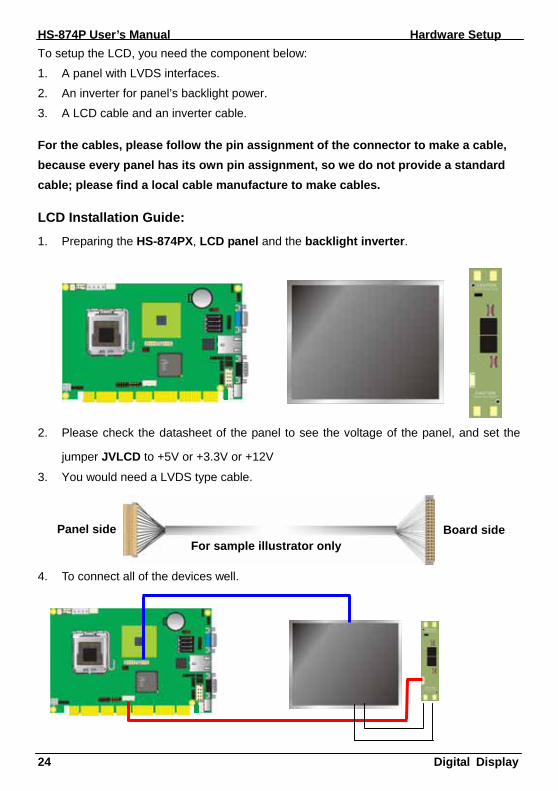
To setup the LCD, you need the component below:
1. A panel with LVDS interfaces.
2. An inverter for panel’s backlight power.
3. A LCD cable and an inverter cable.
For the cables, please follow the pin assignment of the connector to make a cable, because every panel has its own pin assignment, so we do not provide a standard cable; please find a local cable manufacture to make cables.
LCD Installation Guide:
1. Preparing the HS-874PX, LCD panel and the backlight inverter.
2. Please check the datasheet of the panel to see the voltage of the panel, and set the
jumper JVLCD to +5V or +3.3V or +12V
3. You would need a LVDS type cable. 4. To connect all of the devices well.
For sample illustrator onlyPanel side Board side

HS-874P User’s Manual Hardware Setup
Digital Display 25
After setup the devices well, you need to select the LCD panel type in the BIOS.
The panel type mapping is list below:
BIOS panel type selection form
Single channel Dual channel NO. Output format NO. Output format
1 800 x 600 (18bit) 3 1280 x 1024 (24bit)
2 1024 x 768 (24bit) 4 1366 x 768 (24bit)

HS-874P User’s Manual Hardware Setup
Digital Display 26
2.8.3 <DVI Display> (HS-874PD only)
The board provides optional DVI-D interface with Intel Q35, compliant with DVI 1.0
standard.
Connector: CN_DVI
Connector type: 26-pin header connector (pitch = 2.0mm)
Pin Number Assignment Pin Number Assignment 1 TX1+ 2 TX1- 3 Ground 4 Ground 5 TXC+ 6 TXC- 7 Ground 8 PVDD 9 N/C 10 N/C 11 TX2+ 12 TX2- 13 Ground 14 Ground 15 TX0+ 16 TX0- 17 N/C 18 HPDET 19 DDCDATA 20 DDCCLK 21 GND 22 N/C 23 N/C 24 N/C 25 N/C 26 N/C
CN_DVI
2
1
26
25

HS-874P User’s Manual Hardware Setup
Onboard Audio Interface 27
2.9 <Onboard Audio Interface> The board provides the onboard HD 2-channel audio interface with Realtek ALC888
Connector: CN_AUDIO Type: 10-pin (2 x 5) header (pitch-2.54mm)
Pin Description Pin Description 1 MIC_L 2 Ground 3 MIC_R 4 ACZ_DET 5 Speaker_R 6 MIC Detect 7 SENSE 8 N/C 9 Speaker_L 10 Speaker Detect
Connector: CDIN Type: 4-pin header (pitch = 2.54mm)
Pin Description 1 CD – Left 2 Ground 3 Ground 4 CD – Right
CN_IN 1
4
10
1 CN_AUDIO
2
9

HS-874P User’s Manual Hardware Setup
USB2.0 Interface 28
2.10 <USB2.0 Interface> Based on Intel ICH9DO, the board provides 4 USB2.0 ports. The USB2.0 interface provides
up to 480Mbps of transferring rate.
Interface USB2.0
Controller ICH9DO
Transfer Rate Up to 480Mb/s
Output Current 500mA
CN_USB1/2
CN_IR1 5
2 10 2 10
1 9 1 9

HS-874P User’s Manual Hardware Setup
USB2.0 Interface 29
Connector: CN_IR Type: 5-pin header for SIR Port
Pin Description 1 Vcc 2 N/C 3 IRRX 4 Ground 5 IRTX
Connector: CN_USB1/2 Type: 10-pin (5 x 2) header for USB Port
Pin Description Pin Description 1 VCC 2 VCC 3 Data0- 4 Data1- 5 Data0+ 6 Data1+ 7 Ground 8 Ground 9 Ground 10 N/C
PS: The USB2.0 will be only active when you connecting with the USB2.0 devices, if you
insert an USB1.1 device, the port will be changed to USB1.1 protocol automatically. The
transferring rate of USB2.0 as 480Mbps is depending on device capacity exact transferring
rate may not be up to 480Mbps.
HS-874P User’s Manual Hardware Setup
Power and Fan Installation 30
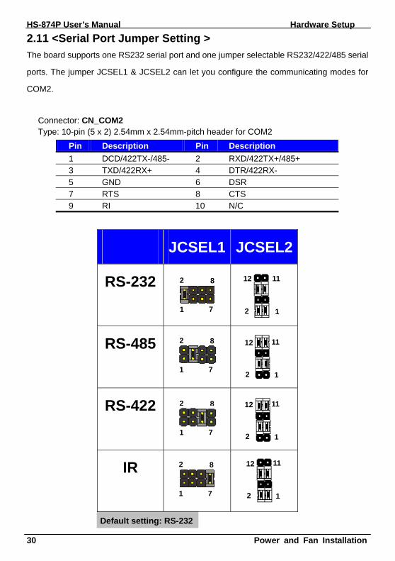
2.11 <Serial Port Jumper Setting > The board supports one RS232 serial port and one jumper selectable RS232/422/485 serial
ports. The jumper JCSEL1 & JCSEL2 can let you configure the communicating modes for
COM2.
Connector: CN_COM2 Type: 10-pin (5 x 2) 2.54mm x 2.54mm-pitch header for COM2
Pin Description Pin Description 1 DCD/422TX-/485- 2 RXD/422TX+/485+ 3 TXD/422RX+ 4 DTR/422RX- 5 GND 6 DSR 7 RTS 8 CTS 9 RI 10 N/C
JCSEL1 JCSEL2
RS-232
RS-485
RS-422
IR
Default setting: RS-232
1
8
7
2
1
8
7
2
1
8
7
2
1
8
7
2
12
2
11
1
12
2
11
1
12
2
11
1
12
2
11
1

HS-874P User’s Manual Hardware Setup
Power and Fan Installation 31
CN_COM2
JCSEL1
JCSEL2
1
8
7
2
12
2
11
1

HS-874P User’s Manual Hardware Setup
Power and Fan Installation 32
2.12 <Power and Fan Installation> The board comes with a 4-pin AT and 4pin 12V power connector for powering the board,
two fan connectors for CPU and system. The board also provides a 3-pin ATX function
connector. You can just connect the two power connectors without any backplane to work.
2.12.1 <Power connectors> Connector: DC_IN Type: 4-pin P-type connector for +5V/+12V input
Pin Description Pin Description Pin Description Pin Description1 +12V 2 Ground 3 Ground 4 +5V
Connector: DC_12V Type: 4-pin P-type connector for +5V/+12V input
Pin Description Pin Description Pin Description Pin Description1 Ground 2 Ground 3 +12V 4 +12V
Connector: CN_PS Type: 3-pin ATX function connector
Pin Description Pin Description Pin Description1 5V Standby 2 Ground 3 Power On

HS-874P User’s Manual Hardware Setup
Power and Fan Installation
33
2.12.2 <Fan Connectors> Connector: CPUFAN Type: 4-pin fan wafer connector
Pin Description Pin Description 1 Ground 2 +12V 3 Fan Speed Detection 4 Fan Control
Connector: SYSFAN Type: 3-pin fan wafer connector
Pin Description Pin Description Pin Description 1 Ground 2 +12V 3 Fan Speed Detection
CPUFAN
1
DC_IN
1 4CN_PS
SYSFAN
1 3
1
3 3
1 2
3 4

HS-874P User’s Manual Hardware Setup
Power and Fan Installation 34
2.13 <GPIO Interface> The board provides a 12-pin General Purpose I/O interface, with programmable 8-bit I/O
(4-bit input & 4-bit output).
Connector: CN_DIO Type: onboard 2 x 6-pin header, pitch=2.0mm
Pin Description Pin Description 1 Ground 2 Ground 3 GP10 4 GP14 5 GP11 6 GP15 7 GP12 8 GP16 9 GP13 10 GP17 11 VCC 12 +12V
CN_DIO
1
12
2
11
HS-874P User’s Manual Hardware Setup
35
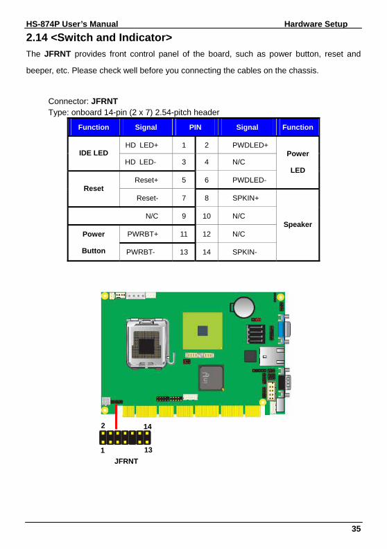
2.14 <Switch and Indicator> The JFRNT provides front control panel of the board, such as power button, reset and
beeper, etc. Please check well before you connecting the cables on the chassis.
Connector: JFRNT Type: onboard 14-pin (2 x 7) 2.54-pitch header
Function Signal PIN Signal Function
HD LED+ 1 2 PWDLED+IDE LED
HD LED- 3 4 N/C
Reset+ 5 6 PWDLED-
Power
LED
Reset Reset- 7 8 SPKIN+
N/C 9 10 N/C
PWRBT+ 11 12 N/C Power
Button PWRBT- 13 14 SPKIN-
Speaker
JFRNT1
142
13

HS-874P User’s Manual
36
(This Page is Left for Blank)

HS-874P User’s Manual
37
Chapter 3 <System Configuration> 3.1 <SATA configuration> SATA Mode:
This option can let you select whether the Serial ATA hard drives would work under normal
IDE mode or RAID mode. The RAID mode need more than one HDD is applied.

HS-874P User’s Manual
38
3.2 <SATA RAID Configuration> The board integrates Intel® ICH9DO with RAID function for Serial ATA II drives, and
supports the configurations below:
RAID 0 (Stripping): Two hard drives operating as one drive for optimized data R/W
performance. It needs two unused drives to build this operation.
RAID 1 (Mirroring): Copies the data from first drive to second drive for data security, and if
one drive fails, the system would access the applications to the workable drive. It needs two
unused drives or one used and one unused drive to build this operation. The second drive
must be the same or lager size than first one.
RAID 5 (striping with parity)
A RAID 5 array contains three or more hard drives where the data is divided into
manageable blocks called strips. Parity is a mathematical method for recreating data that
was lost from a single drive, which increases fault-tolerance. The data and parity are striped
across all the hard drives in the array. The parity is striped in a rotating sequence to reduce
bottlenecks associated with the parity calculations.
RAID 10 (RAID 0+1)
A RAID 10 array uses four hard drives to create a combination of RAID levels 0 and 1. The
data is striped across a two-drive array forming the RAID 0 component. Each of the drives
in the RAID 0 array is then mirrored by a RAID 1 component.
Intel Matrix Storage Technology: This technology would allow you to use RAID 0+1 mode
on only two drives (4 drives needed on traditional RAID 0+1). It will create two partitions on
each hard drive to simulate RAID 0 and RAID 1. It also can let you modify the partition size
without re-formatted.
For more information of Intel Matrix S4torage Technology, please visit Intel’s website.
If you need to install an operation system on the RAID set, please use the driver disk
attached in the package when it informs you to obtain the RAID drivers.

HS-874P User’s Manual
39
Please press <CTRL+I> to enter the RAID configuration menu.
You can setup the RAID under operation system for Microsoft® Windows XP SP1, please
install the Intel® Application Accelerator Ver.7.8 later to support RAID configuration with
Intel® Matrix Storage Technology.
1. After installing Intel Application Accelerator, please execute Intel® Storage Utility.
Demo configuration for 2 SATA Drives and set as Intel Matrix Storage Technology set
HS-874P User’s Manual
40
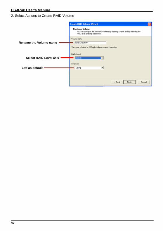
2. Select Actions to Create RAID Volume
Rename the Volume name
Select RAID Level as 0
Left as default

HS-874P User’s Manual
41
3. Please select two hard drives to prepare to set the RAID volume
4. Specify the Volume size
5. Repeat the step 1 to create second volume as RAID Level 1.
Tune this bar to specify the volume size, if you specify the volume size lower than maximum, you can create a secondvolume for another RAID set. (Make RAID 0+1 on only two hard drives)
For other configuration set please click Help on tool bar.

HS-874P User’s Manual
42
3.3 <Audio Configuration> The board integrates Intel® ICH9DO with REALTEK® ALC888 code. It can support
2-channels sound under system configuration. Please follow the steps below to setup your
sound system.
1. Install REALTEK HD Audio driver.
2. Lunch the control panel and Sound Effect Manager.
3. Select Speaker Configuration
4. Select the sound mode to meet your speaker system.

HS-874P User’s Manual BIOS Setup
BIOS Setup 43
3.4 <Video Memory Setup> Based on Intel® Q35 chipset with GMA (Graphic Media Accelerator) 3100, the board
supports Intel® DVMT (Dynamic Video Memory Technology) 3.0, which would allow the
video memory be triggered up to 384MB.
To support DVMT, you need to install the Intel GMA 3100 Driver with supported OS.
BIOS Setup:
On-Chip Frame Buffer Size:
This item can let you select video memory which been allocated for legacy VGA and SVGA
graphics support and compatibility. The available option is 1MB and 8MB.
DVMT Mode:
This item can let you select Graphics shared memory DVMT or Fixed.
DVMT/FIXED Memory Size:
This item can let you select size of video memory, the system would configure the video
memory depends on your application, If set DVMT mode this item is strongly recommend to
be selected as MAX.

HS-874P User’s Manual System Configuration
Audio Setup 44
System
Memory
On-Chip Frame
Buffer Size
Fixed Memory
Size
DVMT Memory
Size
Total Graphic Memory
1MB 128MB 0MB 128MB 1MB 0MB 128MB 128MB 8MB 128MB 0MB 128MB
256MB ~ 511MB
8MB 0 128MB 128MB 1MB 128MB 0 128MB 1MB 256MB 0 256MB 1MB 0 128MB 128MB 1MB 0 256MB 256MB 8MB 128MB 0 128MB 8MB 256MB 0 256MB 8MB 0 128MB 128MB
512MB~1023MB
8MB 0 256MB 256MB 1MB 128MB 0 128MB 1MB 256MB 0 256MB 1MB 0 128MB 128MB 1MB 0 256MB 256MB 1MB 0 MAX 384MB 8MB 128MB 0 128MB 8MB 256MB 0 256MB 8MB 0 128MB 128MB 8MB 0 256MB 256MB
1024MB upper
8MB 0 MAX 384MB
Notice:
1. The On-Chip Frame Buffer Size would be included in the Fixed Memory.
2. Please select the memory size according to this table.

HS-874P User’s Manual BIOS Setup
BIOS Setup 45
Chapter 4 <BIOS Setup> The motherboard uses the Award BIOS for the system configuration. The Award BIOS in the single board computer is a customized version of the industrial standard BIOS for IBM PC AT-compatible computers. It supports Intel x86 and compatible CPU architecture based processors and computers. The BIOS provides critical low-level support for the system central processing, memory and I/O sub-systems. The BIOS setup program of the single board computer let the customers modify the basic configuration setting. The settings are stored in a dedicated battery-backed memory, NVRAM, retains the information when the power is turned off. If the battery runs out of the power, then the settings of BIOS will come back to the default setting. The BIOS section of the manual is subject to change without notice and is provided here for reference purpose only. The settings and configurations of the BIOS are current at the time of print, and therefore they may not be exactly the same as that displayed on your screen. To activate CMOS Setup program, press <DEL> key immediately after you turn on the system. The following message “Press DEL to enter SETUP” should appear in the lower left hand corner of your screen. When you enter the CMOS Setup Utility, the Main Menu will be displayed as Figure 4-1. You can use arrow keys to select your function, press <Enter> key to accept the selection and enter the sub-menu.
Figure 4-1 CMOS Setup Utility Main Screen

HS-874P User’s Manual
46
(This Page is Left for Blank)
HS-874P User’s Manual
AT Keyboard Port 47
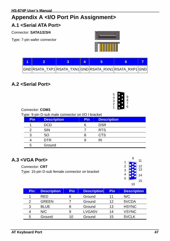
Appendix A <I/O Port Pin Assignment> A.1 <Serial ATA Port> Connector: SATA1/2/3/4
Type: 7-pin wafer connector
1 2 3 4 5 6 7
GND RSATA_TXP1 RSATA_TXN1 GND RSATA_RXN1 RSATA_RXP1 GND
A.2 <Serial Port>
Connector: COM1 Type: 9-pin D-sub male connector on I/O l bracket
Pin Description Pin Description 1 DCD 6 DSR 2 SIN 7 RTS 3 SO 8 CTS 4 DTR 9 RI 5 Ground
A.3 <VGA Port> Connector: CRT Type: 15-pin D-sub female connector on bracket
Pin Description Pin Description Pin Description1 RED 6 Ground 11 N/C 2 GREEN 7 Ground 12 5VCDA 3 BLUE 8 Ground 13 HSYNC 4 N/C 9 LVGA5V 14 VSYNC 5 Ground 10 Ground 15 5VCLK
12345
11
1213
14
15
6
10
54321
9876
HS-874P User’s Manual
AT Keyboard Port 48
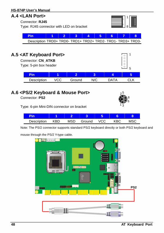
A.4 <LAN Port> Connector: RJ45 Type: RJ45 connector with LED on bracket
Pin 1 2 3 4 5 6 7 8 Description TRD0+ TRD0- TRD1+ TRD2+ TRD2- TRD1- TRD3+ TRD3-
A.5 <AT Keyboard Port>
Connector: CN_ATKB Type: 5-pin box header
Pin 1 2 3 4 5 Description VCC Ground N/C DATA CLK
A.6 <PS/2 Keyboard & Mouse Port>
Connector: PS2
Type: 6-pin Mini-DIN connector on bracket
Pin 1 2 3 5 6 8 Description KBD MSD Ground VCC KBC MSC
Note: The PS/2 connector supports standard PS/2 keyboard directly or both PS/2 keyboard and
mouse through the PS/2 Y-type cable.
1
5
1
2
3
PS2
1
8
5
68

HS-874P User’s Manual
49
(This Page is Left for Blank)

HS-874P User’s Manual Flash BIOS
BIOS Auto Flash Tool 50
Appendix B <Flash BIOS> B.1 <BIOS Auto Flash Tool>
The board is based on Award BIOS and can be updated easily by the BIOS auto flash tool. You can download the tool online at the address below: TUhttp://www.award.com UT TUhttp://www.commell.com.tw/support/support.htmUT File name of the tool is “awdflash.exe”, it’s the utility that can write the data into the BIOS flash ship and update the BIOS.
B.2 <Flash Method> 1. Please make a bootable floppy disk. 2. Get the last .bin files you want to update and copy it into the disk. 3. Copy awardflash.exe to the disk. 4. Power on the system and flash the BIOS. (Example: C:/ awardflash XXX.bin) 5. Re-star the system. Any question about the BIOS re-flash please contact your distributors or visit the web-site at below: http://www.commell.com.tw/support/support.htm

HS-874P User’s Manual System Resources
I/O Port Address Map
51
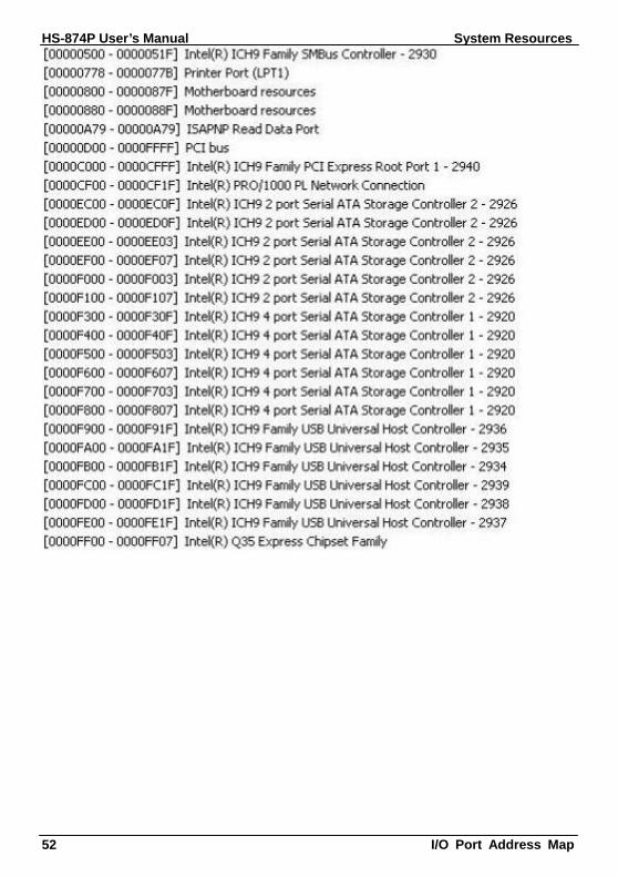
Appendix C <System Resources> C.1 <I/O Port Address Map>
HS-874P User’s Manual System Resources
I/O Port Address Map 52
HS-874P User’s Manual Programming GPIO’s
Programming GPIO’s 53
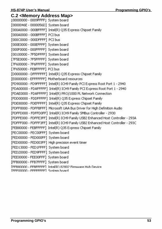
C.2 <Memory Address Map>

HS-874P User’s Manual Watch Dog timer Setting
Programming GPIO’s 54
C.3 <System IRQ Resources>

HS-874P User’s Manual Programming GPIO’s
Programming GPIO’s 55
Appendix D <Programming GPIO’s> The GPIO can be programmed with the MSDOS debug program using simple
IN/OUT commands. The following lines show an example how to do this.
GPIO0...GPIO7 bit0……bit7
-o 2E 87 ;enter configuration
-o 2E 87
-o 2E 2A
-o 2F FD ;enable GPIO function
-o 2E 07
-o 2F 07 ;enable GPIO configuration
-o 2E F0
-o 2F xx ;set GPIO as input/output; set ‘1’ for input,’0’for output
-o 2E F1
-o 2F xx ;if set GPIO’s as output, in this register its value can be set
Optional :
-o 2E F2
-o 2F xx ; Data inversion register ; ‘1’ inverts the current value of the bits ,’0’
leaves them as they are
-o 2E 30
-o 2F 01 ; active GPIO’s
For further information, please refer to Winbond W83627DHG datasheet.

HS-874P User’s Manual Watch Dog timer Setting
Watch Dog timer Setting 56
Appendix E <Watch Dog timer Setting > The watchdog timer makes the system auto-reset while it stops to work for a period. The
integrated watchdog timer can be setup as system reset mode by program.
Timeout Value Range - 1 to 255 - Second or Minute Program Sample Watchdog timer setup as system reset with 5 second of timeout
2E, 87 2E, 87 2E, 07 2F, 08 Logical Device 8 2E, 30 2F, 01 Activate 2E, F5 2F, 00 Set as Second* 2E, F6 2F, 05 Set as 5
* Minute: bit 3 = 0; Second: bit 3 = 1 You can select Timer setting in the BIOS, after setting the time options, the system will reset according to the period of your selection.

HS-874P User’s Manual
57
(This Page is Left for Blank)

HS-874P User’s Manual Contact Information
Contact Information 58
Contact Information
Any advice or comment about our products and service, or anything we can help you please don’t hesitate to contact with us. We will do our best to support you for your products, projects and business
Taiwan Commate Computer Inc. Address 19F, No. 94, Sec. 1, Shin Tai Wu Rd., Shi Chih
Taipei Hsien, Taiwan
TEL +886-2-26963909
FAX +886-2-26963911
Website http://www.commell.com.tw
E-Mail [email protected] (General Information) [email protected] (Technical Support)
Commell is our trademark of industrial PC division