How to use the BT HTS RX R2 evaluation board - st.com · The demo-board BT_HTS_RX_R2 facilitates...
28
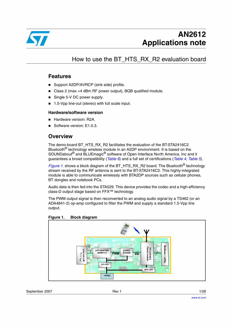
September 2007 Rev 1 1/28 AN2612 Applications note How to use the BT_HTS_RX_R2 evaluation board Features ! Support A2DP/AVRCP (sink side) profile. ! Class 2 (max +4 dBm RF power output), BQB qualified module. ! Single 5-V DC power supply. ! 1.5-Vpp line-out (stereo) with full scale input. Hardware/software version ! Hardware version: R2A. ! Software version: E1.0.3. Overview The demo-board BT_HTS_RX_R2 facilitates the evaluation of the BT-STA2416C2 Bluetooth ® technology wireless module in an A2DP environment. It is based on the SOUNDabout ® and BLUEmagic ® software of Open Interface North America, Inc and it guarantees a broad compatibility (Table 6) and a full set of certifications (Table 4, Table 5). Figure 1. shows a block diagram of the BT_HTS_RX_R2 board. The Bluetooth ® technology stream received by the RF antenna is sent to the BT-STA2416C2. This highly-integrated module is able to communicate wirelessly with BTA2DP sources such as cellular phones, BT dongles and notebook PCs. Audio data is then fed into the STA529. This device provides the codec and a high-efficiency class-D output stage based on FFX™ technology. The PWM output signal is then reconverted to an analog audio signal by a TS462 (or an ADA4841-2) op-amp configured to filter the PWM and supply a standard 1.5-Vpp line output. Figure 1. Block diagram S S T T L L C C 2 2 4 4 1 1 6 6 C C 2 2 C C l l a a s s s s 2 2 m m o o d d u u l l e e CODEC STA529 LPF+BUFFER AD4811-2 L L i i n n e e o o u u t t L L / / R R 1 1 V V p p p p 3V3 LDO +5VDC 3V3 LDO SSI PWM B B u u t t t t o o n n s s / / L L E E D D s s 1.5 Vpp www.st.com
Transcript of How to use the BT HTS RX R2 evaluation board - st.com · The demo-board BT_HTS_RX_R2 facilitates...
September 2007 Rev 1 1/28
AN2612Applications note
How to use the BT_HTS_RX_R2 evaluation board
Features! Support A2DP/AVRCP (sink side) profile.
! Class 2 (max +4 dBm RF power output), BQB qualified module.
! Single 5-V DC power supply.
! 1.5-Vpp line-out (stereo) with full scale input.
Hardware/software version
! Hardware version: R2A.
! Software version: E1.0.3.
OverviewThe demo-board BT_HTS_RX_R2 facilitates the evaluation of the BT-STA2416C2 Bluetooth® technology wireless module in an A2DP environment. It is based on the SOUNDabout® and BLUEmagic® software of Open Interface North America, Inc and it guarantees a broad compatibility (Table 6) and a full set of certifications (Table 4, Table 5).
Figure 1. shows a block diagram of the BT_HTS_RX_R2 board. The Bluetooth® technology stream received by the RF antenna is sent to the BT-STA2416C2. This highly-integrated module is able to communicate wirelessly with BTA2DP sources such as cellular phones, BT dongles and notebook PCs.
Audio data is then fed into the STA529. This device provides the codec and a high-efficiency class-D output stage based on FFX™ technology.
The PWM output signal is then reconverted to an analog audio signal by a TS462 (or an ADA4841-2) op-amp configured to filter the PWM and supply a standard 1.5-Vpp line output.
Figure 1. Block diagram
SS TT LL CC22 44 11 66 CC
22 CC
ll aa ss ss 22 mmoo dd uu ll ee
CCOODDEECC SSTTAA552299
LLPPFF++BBUUFFFFEERR AADD44881111--22
LL ii nn ee oo uu tt LL // RR 11 VV pp pp
33VV33 LLDDOO
++55VVDDCC
33VV33 LLDDOO
SSSSII PPWWMM
BBuu tt tt oo nn ss
// LL EE DDss
1.5 Vpp
www.st.com

Contents AN2612
2/28
Contents
1 Picture and port description . . . . . . . . . . . . . . . . . . . . . . . . . . . . . . . . . . 3
2 Board configurations . . . . . . . . . . . . . . . . . . . . . . . . . . . . . . . . . . . . . . . . 4
2.1 Electrical specifications . . . . . . . . . . . . . . . . . . . . . . . . . . . . . . . . . . . . . . . 5
3 Design information . . . . . . . . . . . . . . . . . . . . . . . . . . . . . . . . . . . . . . . . . . 6
3.1 Schematics . . . . . . . . . . . . . . . . . . . . . . . . . . . . . . . . . . . . . . . . . . . . . . . . . 6
3.2 Bill of materials . . . . . . . . . . . . . . . . . . . . . . . . . . . . . . . . . . . . . . . . . . . . . . 9
3.3 Gerber . . . . . . . . . . . . . . . . . . . . . . . . . . . . . . . . . . . . . . . . . . . . . . . . . . . 12
3.4 Design information for power management . . . . . . . . . . . . . . . . . . . . . . . 14
3.4.1 Recommendations for the codec layout . . . . . . . . . . . . . . . . . . . . . . . . . 14
3.4.2 Power supply considerations . . . . . . . . . . . . . . . . . . . . . . . . . . . . . . . . . 14
3.5 Ground planes . . . . . . . . . . . . . . . . . . . . . . . . . . . . . . . . . . . . . . . . . . . . . 16
3.6 EMI . . . . . . . . . . . . . . . . . . . . . . . . . . . . . . . . . . . . . . . . . . . . . . . . . . . . . . 18
4 Audio performance testing of the board . . . . . . . . . . . . . . . . . . . . . . . . 19
4.1 Test set-up . . . . . . . . . . . . . . . . . . . . . . . . . . . . . . . . . . . . . . . . . . . . . . . . 19
4.2 FFT results . . . . . . . . . . . . . . . . . . . . . . . . . . . . . . . . . . . . . . . . . . . . . . . . 20
4.3 Test result with STM529AD (STM analog dongle) . . . . . . . . . . . . . . . . . . 21
5 Appendix . . . . . . . . . . . . . . . . . . . . . . . . . . . . . . . . . . . . . . . . . . . . . . . . . 23
5.1 Overview of BT-STA2416C2 module . . . . . . . . . . . . . . . . . . . . . . . . . . . . 23
5.2 Certification of Bluetooth® module . . . . . . . . . . . . . . . . . . . . . . . . . . . . . . 24
5.3 Interoperability list . . . . . . . . . . . . . . . . . . . . . . . . . . . . . . . . . . . . . . . . . . 25
6 Trademark and other acknowledgements . . . . . . . . . . . . . . . . . . . . . . . 26
7 Revision history . . . . . . . . . . . . . . . . . . . . . . . . . . . . . . . . . . . . . . . . . . . 27

AN2612 Picture and port description
3/28
1 Picture and port description
Figure 2. Ports available on the board
Table 1. Port description
Port name Description Port name Description
J5 5-V DC power supply S3 Volume -
J1 Proprietary connector S4 Volume +
J3 Audio line out, right channel S5 Play / Pause
J4 Audio line out, left channel D1 BT link indicator
J2 External antenna connector D3 Reserved
S1 Reset button D4 Standby
S2 Reserved D5 Reserved
AntennaLine out
Vol-
Vol+
Play/pause
Standby
Connected
ResetProprietary connector5 V DC supply

Board configurations AN2612
4/28
2 Board configurations
Figure 3. Configuration 1
Figure 4. Configuration 2
HHoommee AAVV ssyysstteemm AAVV ppllaayyeerr ssyysstteemm LLiinnee iinn
Audio Amplifier
BT_HTS_RX_R2 Line out J3 J4
J2
J5
power supply= +5VDC
BBlluueettooootthh aannaalloogg ddoonnggllee ((SSTT ssoolluuttiioonn:: AADD552299))
OORR
EEmmbbeeddddeedd ssyysstteemm 11::
HHoommee AAVV ssyysstteemm AAVV ppllaayyeerr ssyysstteemm
Audio Amplifier
BT_HTS_RX_R2
Line out
J3 J4
J2
J5 +5VDC
BBlluueettooootthh aannaalloogg ddoonnggllee ((SSTT ssoolluuttiioonn:: AADD552299))
OORR
EEmmbbeeddddeedd ssyysstteemm 22::
AAuuddiioo SSRRCC SSwwiittcchheerr

AN2612 Board configurations
5/28
2.1 Electrical specifications (VCCin = 5.0 V and ambient temperature = 25° C unless otherwise specified)
Table 2. Electrical characteristics
Symbol Parameter Conditions Min Typ Max Unit
VCCin Board power supply 4.5 5.0 16 V
IddwSupply current (working mode)
Bluetooth® technology streaming mode, CODEC in binary mode
- 72 80 mA
IddnSupply current (working mode, no streaming)
Bluetooth® technology module connected, no data streaming, CODEC in binary mode
- 57 65 mA
IddsSupply current (standby mode)
Bluetooth® technology module not connected.
- 44 50 mA
Vlineout Signal voltage on line out
Bluetooth® technology streaming mode, IVT BlueSoleil™, full-scale streaming 1-kHz sine wave, CODEC in binary mode
1.4 1.5 1.6 Vpp
Rout Line-out impedance (L, R) - 1 3.6 10 Ω
PRFout RF output power Bluetooth® technology linked -6 <4 4 dBm
Zout RF output impedance(J2) - - 50 - Ω
VSWR Return loss - - - 2.8 dB
THD+NTotal harmonic distortion+noise (L, R)
Test with Bluetooth® technology USB dongle, IVT BlueSoleil™ Version 1.4.8.1, 1-kHz sine wave full scale input, 1-Vpp line out, 20-20 kHz.
- 0.089 0.1 %
SNRSignal to noise ratio (L, R) (no weighting)
Test with Bluetooth® technology USB dongle, IVT BlueSoleil™ version 1.4.8.1, 1-kHz sine wave full scale input, 1-Vpp line out, 20-20 kHz.
72 - - dB

Design information AN2612
6/28
3 Design information
3.1 Schematics
Figure 5. Receiver stage

AN2612 Design information
7/28
Figure 6. Codec and PWM stage
Design information AN2612
8/28
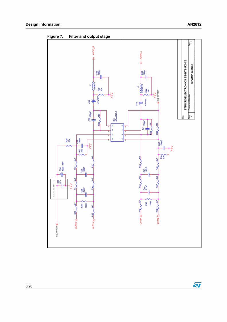
Figure 7. Filter and output stage

AN2612 Design information
9/28
3.2 Bill of materials
Table 3. BOM for BT_HTS_RX_R2 (V01)
Item Ref Qty Designator Part Footprint Remarks
1 CAP 2 C1, C16 10 µF, 16 V CE45Aluminium capacitor 4.5mm
2 CAP 16C2, C3, C4, C5, C8, C10, C13, C14, C18, C19, C20, C24, C26, C29, C32, C48
100 nF 0603
3 CAP 1 C6 82 pF 0603
4 CAP 2 C7, C9 22 pF 0603
5 CAP 1 C11 220 pF 0603
6 CAP 4 C12, C15, C17, C22 10 nF 0603
7 CAP 1 C21 220 µF 16 V CE66Aluminium capacitor 6.6mm
8 CAP 2 C23, C25 1 µF 0805
9 CAP 2 C31, C47 1 µF 0603
10 CAP 1 C27 220 µF, 16 V CE83Aluminium capacitor 8.3mm
11 CAP 1 C28 3.3 µF, 6.3 V CE66Aluminium capacitor 6.6mm
12 CAP 1 C33 0.1 µF 0603
13 CAP 1 C34 100 µF, 16 V CE66Aluminium capacitor 6.6mm
14 CAP 2 C35, C44 2.2 nF 0603
15 CAP 6C36, C37, C38, C41, C45, C46
150 pF 0603
16 CAP 2 C39, C42 47 µF, 16 V CE66Aluminium capacitor 6.6mm
17 CAP 2 C40, C43 100 pF 0603
18 CAP 1 C49 3.3 µF, 6.3 V CE45Aluminium capacitor 4.5mm
19 LED 1 D1Blue, high efficiency
0805
20 DIODE 1 D2 1SS335 0805
21 LED 3 D3, D4, D5Green, high efficiency
0805

Design information AN2612
10/28
22 DIODE 1 TMBYV10-60 DiodeCan take replacement
23 IC 1 IC1 BT-STA2416C2
24 IC 1 IC2 STA529QFN QFN52
25 IC 1 IC3 LD2985AM18 SOT23-5L
26 IC 1 IC4 TS462 MSOP8Alternative:ADA4841-2
27 IC 2 IC5, IC6 LD2985AM33 SOT23-5L
28 CON 1 J1 CON8A2 x 4-pin step 2.54mm
29 CON 1 J2 CON5 SMA
30 CON 1 J3 RIGHT RCA
31 CON 1 J4 LEFT RCA
32 CON 1 J5 CON2 DC jack
33 BEAB 2 L1, L2 FERRITE 0805
34 RES 6R1, R2, R20, R21, R52, R53
1 kΩ 0603
35 RES 15R3, R7, R9, R10, R12, R13, R14, R15, R16, R17, R18, R19, R24, R28, R51
0 Ω 0603
36 RES 3 R4, R39, R44 10 kΩ 0603
37 RES 1 R6 100 Ω 0603
38 RES 1 R8 3.3 kΩ 0603
39 RES 1 R22 1 MΩ 0603
40 RES 1 R23 12 kΩ 0603
41 RES 1 R25 470 Ω 0603
42 RES 2 R26, R27 1.1 Ω 0603
43 RES 4 R29, R33, R49, R50 30 kΩ 0603
44 RES 12R30, R31, R32, R35, R36, R37, R40, R41, R42, R46, R47, R48
4.7 kΩ 0603
45 RES 2 R34, R45 1.5 kΩ 0603
46 RES 2 R38, R43 15 kΩ 0603
47 SW 5 S1, S2, S3, S4, S5 KSR221J KSR221JCan take replacement
48 TP 1 TP1 RST 1 pin not soldered
49 TP 1 TP2 PWREN 1 pin not soldered
50 TP 1 TP3 BOOT 1 pin not soldered
Table 3. BOM for BT_HTS_RX_R2 (V01) (continued)
Item Ref Qty Designator Part Footprint Remarks

AN2612 Design information
11/28
51 TP 1 TP4 USB VCC 1 pin not soldered
52 TP 1 TP5 3.3V 1 pin not soldered
53 TP 1 TP6 UART_TXD 1 pin not soldered
54 TP1 1 TP7 GND 1 pin not soldered
55 TP 1 TP8 UART_RXD 1 pin not soldered
56 TP 1 TP11 AUDIO_L 1 pin not soldered
57 TP 1 TP13 AUDIO_R 1 pin not soldered
58 TP 1 TP14 BT_RESET 1 pin not soldered
59 Crystal 1 Y1 13 MHz 49SX
Table 3. BOM for BT_HTS_RX_R2 (V01) (continued)
Item Ref Qty Designator Part Footprint Remarks

Design information AN2612
12/28
3.3 Gerber
Figure 8. Silkscreen - top
Figure 9. Silkscreen - bottom (viewed from top of board)
AN2612 Design information
13/28
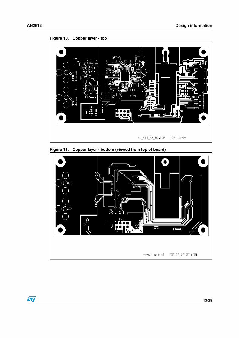
Figure 10. Copper layer - top
Figure 11. Copper layer - bottom (viewed from top of board)

Design information AN2612
14/28
3.4 Design information for power management
3.4.1 Recommendations for the codec layout
" Use an electrolytic capacitor at each branch of the Vcc power track.
" Place decoupling capacitors as close as possible to the Vcc and ground pins.
" Dissipate the heat with a large ground plane.
" Place the PLL filter components as close as possible to pin FILT.
" For differential applications create symmetrical paths for the output stage.
Please refer to the STA529 datasheet/applications note for details of the above points.
3.4.2 Power supply considerations
The Bluetooth® technology transmitter and receiver are alternately switching on and off and there is a risk that the switching noise will appear on the power supply lines. Furthermore this switching frequency is in the audio band. So, if the supply is shared with the audio stage and insufficient decoupling is employed, it could lead to a noisy audio line output when used in single-ended mode, as shown in Figure 13, upper photo. In order to minimize this possibility it was decided to employ separate regulators on the BT_HTS_RX_R2 board for the RF part and for the analog audio part. The lower photo of Figure 13 shows the resulting line output for single-ended mode.
Figure 12 shows how the power management is implemented on the board. IC5, IC6 are two 3.3 V low dropout (LDO) regulators (ST reference LD2985AM33). 3V3_BT is the supply for Bluetooth® technology module, and 3V3_REG is that for the STA529Q (codec). Other brands of LDO are also usable, but they should have a high PSRR and a good regulation rate. Switching type DC/DC power supplies are also workable for the Bluetooth® module supply.
Figure 12. Power management

AN2612 Design information
15/28
Figure 13. Line output noise with Bluetooth module active, no streaming
Common Bluetooth / audio power supply
BT_HTS_RX_R2 two-regulator supply

Design information AN2612
16/28
3.5 Ground planesAs usual, good grounding is very important for audio products. Since BT_HTS_RX_R2 is a mixed analog and digital signal board, the ground connections were considered very carefully.
" RF grounding below the BT-STA2416C2 module is separate from the other modules, and is connected to the main ground inside the BT-STA2416C2 module.
Figure 14 shows the antenna and RF grounding for improved RF reception.
Figure 14. Antenna and RF grounding

AN2612 Design information
17/28
" Bluetooth® technology digital ground, codec digital ground, codec analog ground, codec PA ground and op-amp analog ground are all separate, and each of them is connected to one main grounding point as shown below in Figure 15 and Figure 16.
Figure 15. Grounding arrangement on schematics
Figure 16. Ground arrangement on layout (bottom view)

Design information AN2612
18/28
Figure 17. Ground arrangement on layout (top view)
3.6 EMIThe EMI was minimized by:
" following the recommendations in Section 3.5 on page 16 for the ground configuration.
" placing the 13-MHz crystal as close as possible to the codec (STA529). The tracks between the crystal and the STA529 oscillator pins were made as short as possible and the IC was well grounded.
" making the tracks from OUT1A, OUT1B, OUT2A and OUT2B of the STA529 to the op-amp as short as possible. For more details on this point please refer to the datasheet and applications note for the STA529.

AN2612 Audio performance testing of the board
19/28
4 Audio performance testing of the board
4.1 Test set-upTesting is done with the Bluetooth® technology V1.2 Class-2 USB dongle, running with IVT BlueSoleil 1.4.8.1 software, streaming 1 kHz sine-wave signal by Windows Media® player 10 on the computer, and measuring with audio precision. The diagram for the set-up is shown below in Figure 18.
Figure 18. Test set-up
IVT Bluesoleil 1.4.8.1 Windows
Bluetooth USB dongle
BT_HTS_RX_R2
J3
J4
J2
J5
External power supply (5 V DC)
Audio precision
Analog Input Channel A Analog Input Channel B

Audio performance testing of the board AN2612
20/28
4.2 FFT results
Figure 19. FFT 0-dBFS input, 3.3 V, 600 Ω
Figure 20. FFT noise floor, 3.3 V, 600 Ω
-140
+0
-130
-120
-110
-100
-90
-80
-70
-60
-50
-40
-30
-20
-10
dBV
20 20k50 100 200 500 1k 2k 5k 10kHz
-140
+0
-130
-120
-110
-100
-90
-80
-70
-60
-50
-40
-30
-20
-10
dBV
20 20k50 100 200 500 1k 2k 5k 10kHz

AN2612 Audio performance testing of the board
21/28
4.3 Test result with STM529AD (STM analog dongle)
Figure 21. FFT 2.36-V, 1-kHz input from STM529AD, 1-Vpp line out
Minimum SNR = 73 dB (A weighting)
Caution: The maximum input level for STM529AD is 2.36 V RMS.
Input s ignal Vrms=2.36v (max)Line out Vpp=1vSNR=73dB(A weighting),(600ohms)
-140
+0
-130
-120
-110
-100
-90
-80
-70
-60
-50
-40
-30
-20
-10
dBV
20 20k50 100 200 500 1k 2k 5k 10kHz

Audio performance testing of the board AN2612
22/28
Figure 22. THD + N vs frequency (2.36-V RMS input, 1-Vpp line out)
Figure 23. Frequency response (0dBr = 1 Vpp, 2.36-V RMS input, 1-Vpp line out)

AN2612 Appendix
23/28
5 Appendix
5.1 Overview of BT-STA2416C2 module
Figure 24. BT-STA2426C2 module
The BT-STA2416C2 module is based on two ICs:
– STA2416 host controller
– STLC2150 RF
Information for the STMicroelectronics ICs.
" Supported interfaces:
– USB (1.1)
– UART
– PCM (pulse code modulation)
" Output power level: Class 2 (max +4 dBm)
" Bluetooth® technology protocol layer support up to HCI
" ACL & SCO links
" Transmission rate up to 721 kbit/s
" Optimized link manager and control
" Support WLAN coexistence
" Integrated 4-Mbit flash, 64-Kbyte RAM, 4-Kbyte ROM
" Single 3.3-V power supply
" Low power consumption
" CE compliant
" Safety EN60950-1 (2001)
" EMC EN301 489 17V1.2.1
" Radio ES 300 328 V1.6
" BQB: RF - HCI - LM - BB
Host ctrl.
STA2416
RF Front-end
STLC2150 RF link
15
mm
30 mm
BT-STA2416C2

Appendix AN2612
24/28
5.2 Certification of Bluetooth® moduleThe STMicroelectronics chipset and modules given in Table 4 are fully compliant with the following BQB certifications under PRD2.0 standard:
The stack supplied by Open Interface North America, Inc. is BQB certified and provides full connectivity for our Bluetooth® technology wireless kit by supporting different profiles.
Table 4. BQB qualified designs (chipset and modules)
Qualified designs
Manufacturer Product IDProduct
typeProfiles QD ID
Bluetoothtechnologymodule
STMicroelectronics
BT_STA2416C2 Component RF, BB, LM, HCI B012535
Table 5. Supported profiles
Qualified designs
Manufacturer Product IDProduct
typeProfiles QD ID
Bluetooth technology stack
Open Interface North America, Inc. BLUEmagic®
3.0
Profilesub-system
SDP, GAP, A2DP, AVCTP, AVDTP, AVRCP, BIP, BNEP, BPP, CTP, DUN, FAX, FTP, GAVDP, HCRP, HFP, HID, HP, ICP, OPP, PAN, RFCOMM, SAP, SDAP, SPP, SYNC, L2CAP
B010293
AN2612 Appendix
25/28
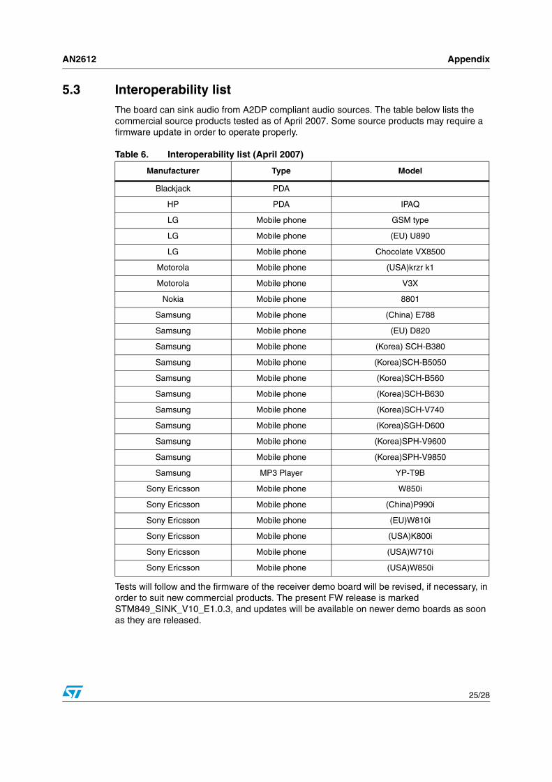
5.3 Interoperability listThe board can sink audio from A2DP compliant audio sources. The table below lists the commercial source products tested as of April 2007. Some source products may require a firmware update in order to operate properly.
Tests will follow and the firmware of the receiver demo board will be revised, if necessary, in order to suit new commercial products. The present FW release is marked STM849_SINK_V10_E1.0.3, and updates will be available on newer demo boards as soon as they are released.
Table 6. Interoperability list (April 2007)
Manufacturer Type Model
Blackjack PDA
HP PDA IPAQ
LG Mobile phone GSM type
LG Mobile phone (EU) U890
LG Mobile phone Chocolate VX8500
Motorola Mobile phone (USA)krzr k1
Motorola Mobile phone V3X
Nokia Mobile phone 8801
Samsung Mobile phone (China) E788
Samsung Mobile phone (EU) D820
Samsung Mobile phone (Korea) SCH-B380
Samsung Mobile phone (Korea)SCH-B5050
Samsung Mobile phone (Korea)SCH-B560
Samsung Mobile phone (Korea)SCH-B630
Samsung Mobile phone (Korea)SCH-V740
Samsung Mobile phone (Korea)SGH-D600
Samsung Mobile phone (Korea)SPH-V9600
Samsung Mobile phone (Korea)SPH-V9850
Samsung MP3 Player YP-T9B
Sony Ericsson Mobile phone W850i
Sony Ericsson Mobile phone (China)P990i
Sony Ericsson Mobile phone (EU)W810i
Sony Ericsson Mobile phone (USA)K800i
Sony Ericsson Mobile phone (USA)W710i
Sony Ericsson Mobile phone (USA)W850i

Trademark and other acknowledgements AN2612
26/28
6 Trademark and other acknowledgements
Bluetooth is a registered trademark of Bluetooth SIG Inc.
SOUNDabout and BLUEmagic are registered trademarks of Open Interface North America, Inc.
FFX is an STMicroelectronics proprietary digital modulation technology.
BlueSoleil is a trademark of IVT Corporation.
Windows Media is a registered trademark of Microsoft Corporation.

AN2612 Revision history
27/28
7 Revision history
Table 7. Document revision history
Date Revision Changes
Sep-2007 1 Initial release.

AN2612
28/28
Please Read Carefully:
Information in this document is provided solely in connection with ST products. STMicroelectronics NV and its subsidiaries (“ST”) reserve theright to make changes, corrections, modifications or improvements, to this document, and the products and services described herein at anytime, without notice.
All ST products are sold pursuant to ST’s terms and conditions of sale.
Purchasers are solely responsible for the choice, selection and use of the ST products and services described herein, and ST assumes noliability whatsoever relating to the choice, selection or use of the ST products and services described herein.
No license, express or implied, by estoppel or otherwise, to any intellectual property rights is granted under this document. If any part of thisdocument refers to any third party products or services it shall not be deemed a license grant by ST for the use of such third party productsor services, or any intellectual property contained therein or considered as a warranty covering the use in any manner whatsoever of suchthird party products or services or any intellectual property contained therein.
UNLESS OTHERWISE SET FORTH IN ST’S TERMS AND CONDITIONS OF SALE ST DISCLAIMS ANY EXPRESS OR IMPLIEDWARRANTY WITH RESPECT TO THE USE AND/OR SALE OF ST PRODUCTS INCLUDING WITHOUT LIMITATION IMPLIEDWARRANTIES OF MERCHANTABILITY, FITNESS FOR A PARTICULAR PURPOSE (AND THEIR EQUIVALENTS UNDER THE LAWSOF ANY JURISDICTION), OR INFRINGEMENT OF ANY PATENT, COPYRIGHT OR OTHER INTELLECTUAL PROPERTY RIGHT.
UNLESS EXPRESSLY APPROVED IN WRITING BY AN AUTHORIZED ST REPRESENTATIVE, ST PRODUCTS ARE NOTRECOMMENDED, AUTHORIZED OR WARRANTED FOR USE IN MILITARY, AIR CRAFT, SPACE, LIFE SAVING, OR LIFE SUSTAININGAPPLICATIONS, NOR IN PRODUCTS OR SYSTEMS WHERE FAILURE OR MALFUNCTION MAY RESULT IN PERSONAL INJURY,DEATH, OR SEVERE PROPERTY OR ENVIRONMENTAL DAMAGE. ST PRODUCTS WHICH ARE NOT SPECIFIED AS "AUTOMOTIVEGRADE" MAY ONLY BE USED IN AUTOMOTIVE APPLICATIONS AT USER’S OWN RISK.
Resale of ST products with provisions different from the statements and/or technical features set forth in this document shall immediately voidany warranty granted by ST for the ST product or service described herein and shall not create or extend in any manner whatsoever, anyliability of ST.
ST and the ST logo are trademarks or registered trademarks of ST in various countries.
Information in this document supersedes and replaces all information previously supplied.
The ST logo is a registered trademark of STMicroelectronics. All other names are the property of their respective owners.
© 2007 STMicroelectronics - All rights reserved
STMicroelectronics group of companies
Australia - Belgium - Brazil - Canada - China - Czech Republic - Finland - France - Germany - Hong Kong - India - Israel - Italy - Japan - Malaysia - Malta - Morocco - Singapore - Spain - Sweden - Switzerland - United Kingdom - United States of America
www.st.com