How to build Digital Load Cells with 1 conveniently
48
Technical Whitepaper 1 ® How to build Digital Load Cells with 1 conveniently March 2010 Document-No.: WP_004_en V1.0
Transcript of How to build Digital Load Cells with 1 conveniently
Technical Whitepaper
1
®
How to build Digital Load Cells with 1 conveniently March 2010Document-No.: WP_004_en V1.0
acam-messelectronic gmbh - Am Hasenbiel 27 - D-76297 Stutensee-Blankenloch - Germany - www.acam.de2
1®
Preface
In the last decades the digital load cell (DLC) was a niche product. This is because the
production is elaborate and expensive. And the number of applications which really make
use of the benefits of the digital load cell concept are limited.
In contrary there is the analog load cell which is still state of the art today. Although
some efforts are also necessary in production here, i.e. gain and offset adjustment, the
manufacturing is well known and practicable. This is the reason, why today’s scales are
mainly equipped with ordinary analog load cells and that they are produced in large quan-
tities.
Indeed, building a digital load cell nowadays means to go (almost) the same way like in
the production of an analog load cell but to set something on top: the digitalization of the
result. In other words the electronics, normally consisting of a converter and a micro-
controller, needs to be added. In respect of calibration the adjustment of the load cell
parameters is done separately from the electronics. Later then, electronics and load cell
are put together and the summary of both errors has to be within legal specifications like
OIML1. The practice in production shows, that doing this means a lot of hand work and
adjustment, paired with loads of tests (e.g. temperature drift tests) to verify conformance
to specification. You can imagine that there is only little room left for automatization and
a significant rise in quality, reliability or speeding up the process. In other words using
the standard production workflow there is no real benefit of the digital load cell compared
with its analog correspondent.
PICOSTRAIN introduces new possiblities here – based on existing production processes –
which can lead to
� a simpler, more effective and reliable production process
� higher quality thanks to a new adjustment. This helps to reach challenging specifica-
tions like OIML 6000 much easier than nowadays
� a full automatic adjustment of gain and zero drift without manual trimming
Saving costs and efforts come automatically with this approach and it allows to think
about the digital load cell as a successor of the analog load cell in a way that it makes
sense in both – technical and commercial aspects!
1 OIML = Organisation Internationale de Métrologie Légale, is an international organization which gives rules and guidelines for legal metrology. Please see www.oiml.org for more information.

acam-messelectronic gmbh - Am Hasenbiel 27 - D-76297 Stutensee-Blankenloch - Germany - www.acam.de 3
This White Paper describes the situation of analog and digital load cells nowadays to-
gether with its potential benefits but also with its limitations. Later then, the concept of
using PICOSTRAIN is explained and its benefit to the production of digital load cells. A
practical example with results of the measurement with a prototype are given in the last
section of the paper.
Authors: Augustin Braun, Ralf Emberger
Preface

acam-messelectronic gmbh - Am Hasenbiel 27 - D-76297 Stutensee-Blankenloch - Germany - www.acam.de
1®
4

acam-messelectronic gmbh - Am Hasenbiel 27 - D-76297 Stutensee-Blankenloch - Germany - www.acam.de 5
Table of Contents
1 PICOSTRAIN Measurement Principle...............................................................9
2. How does PICOSTRAIN make the production easier? .......................................11
2.1 Temperature Compensation .................................................................11
2.1.1 Compensation resistor Rspan .................................................. 16
2.1.2 Nonlinearity of gain over temperature ........................................ 17
2.2 Mounting and Assembling ....................................................................19
3. Advantages by building a digital load cell with PICOSTRAIN ...............................23
3.1 Cost Saving by Simplified Production ......................................................23
3.2 Calibration .........................................................................................23
3.3 Low Current ......................................................................................24
3.3.1 Self Heating ........................................................................... 25
3.4 EMI behavior ......................................................................................26
3.5 Commercial aspects ...........................................................................27
3.6 Digital Load Cells in Standard Scales .....................................................27
4. Prototype .................................................................................................31
4.1 Set-Up ..............................................................................................31
4.2 Noise Figures and Stabilization Time ......................................................33
4.3 Temperature Compensation Results ......................................................35
4.4 Current Consumption ..........................................................................38
4.5 Interface ...........................................................................................38
4.6 Future Options ...................................................................................39
4.7 Conclusion .........................................................................................41
A. Appendix ..................................................................................................43
A.1 Schematics .......................................................................................43
A.2 Layout ..............................................................................................44
A.3 Bill of Material ....................................................................................46
A.4 Literature Guide .................................................................................47

acam-messelectronic gmbh - Am Hasenbiel 27 - D-76297 Stutensee-Blankenloch - Germany - www.acam.de6
1®
Current Situation
Nowadays digital load cells are still niche products. They are available as calibrated C3
and C6 cells as well as uncalibrated types. Typical applications are set-ups with long wires
(where the digital signal transmission is better than analog), when several load cells are
processed by one single controller, e.g. truck scales or in electromagnetical noisy envi-
ronments.
The advantages can therefore be concluded as:
� Long cable lengths possible without loss in signal strength
� Combination of several load cells processed by a single processor
� Reduced sensitivity to EMI
� Good replaceability as intrinsically calibrated cells
In order to get a more detailed picture of what a digital load cell is or how its concept is
like we have a look at its set-up nowadays. As mentioned in the introduction it basically
consists of the load cell itself combined with the electronics which is a converter and a
microcontroller:
Fig. 1: Digital Load Cell set-up nowadays
The signal generated by the strain gages on the load cell are given to the elect-
ronics. Here an A/D converter digitizes the analog signal and feeds the micro-
controller or DSP with the A/D raw count. The controller processes then the
raw values, corrects them in terms of linearization, filtering, hysteresis, etc. and
finally puts out the digital signal.

acam-messelectronic gmbh - Am Hasenbiel 27 - D-76297 Stutensee-Blankenloch - Germany - www.acam.de 7
Although the concept of the digital load cell fits quite well into some applications, the
acceptance as a serious replacement for the analog load cell is only moderate so far. The
reason for that lies in the production of the DLCs which is quite elaborate and costly. This
makes it difficult to produce them in higher quantities with reliable quality and as a conse-
quence the quantities are only increasing slowly.
But what is it that makes it difficult to automatize the production and/or lower production
costs?
- Well, as you can imagine the main obstacles come from the calibration part and to
meet specifications for certified load cells, especially the limits for temperature drift. A
nowadays production of digital load cells faces the following items amongst others:
� Mounting and assembling of load cell and electronics separately
� Calibration of load cell and electronics separately, the summary error needs to match
legal specifications
� High efforts are needed for temperature compensation of gain and offset
� Manual trimming of the load cell’s adjustment resistors means a lot of hand work
� Long throughput times due to iterative temperature drift tests
The items make clear, that there is only limited space for automatization as many pro-
cessing steps can only be made manually (by hand). Speaking from a commercial point of
view we can conclude that costs cannot be lowered with today’s production workflow and
therefore demand for digital load cells is still moderate due to high prices.
This is where PICOSTRAIN comes into the game. We think that serving both aspects –
technically and commercially – our technology offers possiblities to produce DLCs more
effectively and therefore faster and cheaper. Fortunately, at the same time quality and
reliability of a more automized production can be realized.
In the next sections we will outline how the PICOSTRAIN technology works and how it can
contribute to the production process of digital load cells.
Current Situation

acam-messelectronic gmbh - Am Hasenbiel 27 - D-76297 Stutensee-Blankenloch - Germany - www.acam.de8
1®
acam-messelectronic gmbh - Am Hasenbiel 27 - D-76297 Stutensee-Blankenloch - Germany - www.acam.de 9
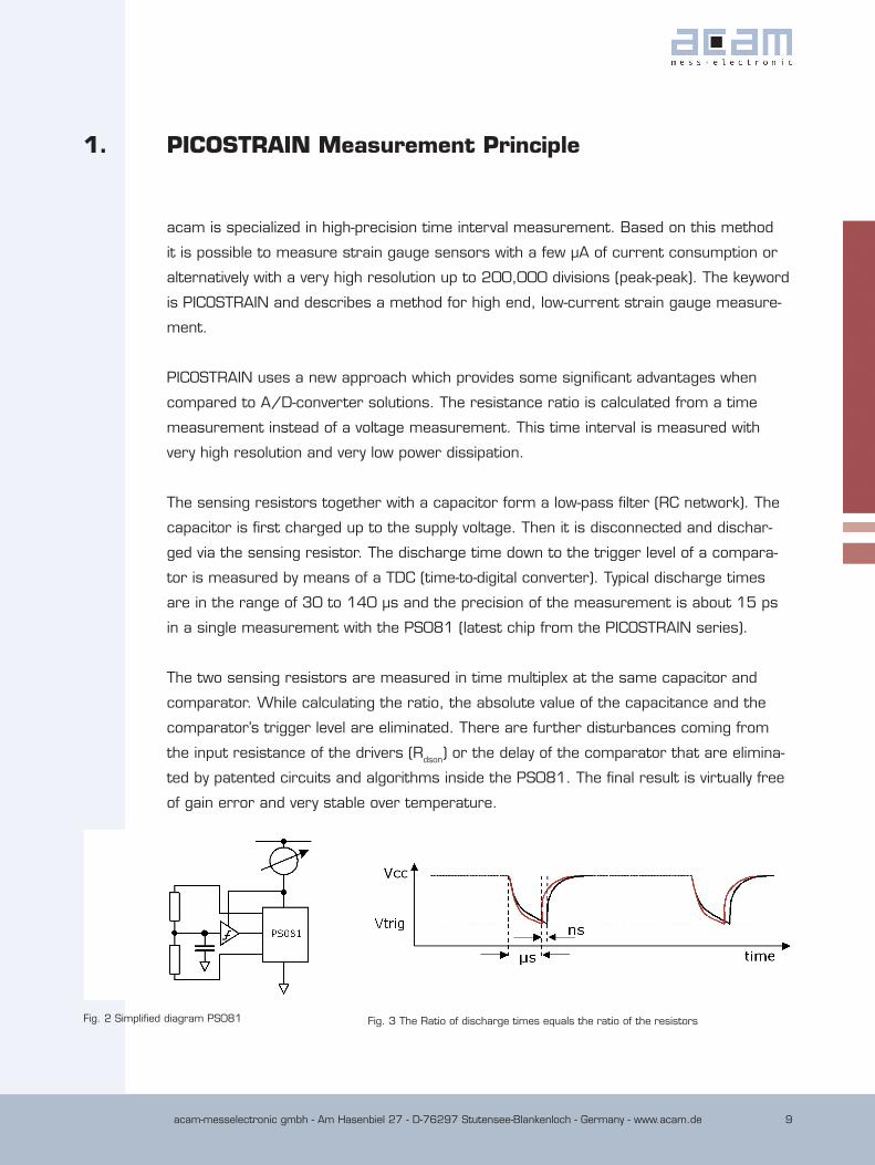
1. PICOSTRAIN Measurement Principle
acam is specialized in high-precision time interval measurement. Based on this method
it is possible to measure strain gauge sensors with a few µA of current consumption or
alternatively with a very high resolution up to 200,000 divisions (peak-peak). The keyword
is PICOSTRAIN and describes a method for high end, low-current strain gauge measure-
ment.
PICOSTRAIN uses a new approach which provides some significant advantages when
compared to A/D-converter solutions. The resistance ratio is calculated from a time
measurement instead of a voltage measurement. This time interval is measured with
very high resolution and very low power dissipation.
The sensing resistors together with a capacitor form a low-pass filter (RC network). The
capacitor is first charged up to the supply voltage. Then it is disconnected and dischar-
ged via the sensing resistor. The discharge time down to the trigger level of a compara-
tor is measured by means of a TDC (time-to-digital converter). Typical discharge times
are in the range of 30 to 140 µs and the precision of the measurement is about 15 ps
in a single measurement with the PS081 (latest chip from the PICOSTRAIN series).
The two sensing resistors are measured in time multiplex at the same capacitor and
comparator. While calculating the ratio, the absolute value of the capacitance and the
comparator’s trigger level are eliminated. There are further disturbances coming from
the input resistance of the drivers (Rdson) or the delay of the comparator that are elimina-
ted by patented circuits and algorithms inside the PS081. The final result is virtually free
of gain error and very stable over temperature.
Fig. 2 Simplified diagram PS081 Fig. 3 The Ratio of discharge times equals the ratio of the resistors

acam-messelectronic gmbh - Am Hasenbiel 27 - D-76297 Stutensee-Blankenloch - Germany - www.acam.de10
1®
acam-messelectronic gmbh - Am Hasenbiel 27 - D-76297 Stutensee-Blankenloch - Germany - www.acam.de10
1.
PICOSTRAIN does not need a full-bridge. Although full bridges can be measured,
due to the measuring principle of PICOSTRAIN, a half bridge is sufficient. Most load
cells consist of a full bridge anyway, which basically is equal to 2 half bridges. Opti-
mal results can be achieved when 2 half bridges are used (a „split-up“ Wheatstone
bridge), we call this kind of full bridge a ‚PICOSTRAIN bridge‘. The sensing resistors
are connected directly to the converter. There is no need for a separate supply of the
sensor. Thanks to the pulsed operation the current through the strain gages is easily
controlled and far below the current of comparable A/D-converter solutions.
With the PS081 it is possible to reach the following benchmark data with respect to
current consumption, maximum resolution and update rate: The current consump-
tion for the complete scale may be reduced to 15 µA when properly set up for this
goal (2,000 scale divisions at 1mV/V sensitivity and 3 Hz update rate). This low va-
lue is possible because of the pulsed manner of operation, the fact that the sensor is
supplied directly from the chip and the reduced update rate. As a further advantage
the self-heating of the sensor is minimized, often practically zero.
The maximum resolution of the PS081 is close to 20 bit effective (1 million eff. divisi-
ons!!) for 2 mV/V sensitivity (common value with strain gages) and 5 Hz update rate.
Referring to the resistance, this means a resolution of almost 29 bit! The maximum
update rate of the PS081 is 1,000 Hz. In general, the parameters, current con-
sumption, resolution and update rate are interrelated and can be adjusted by confi-
guration.
PICOSTRAIN Measurement Principle
acam-messelectronic gmbh - Am Hasenbiel 27 - D-76297 Stutensee-Blankenloch - Germany - www.acam.de 11
2. How does PICOSTRAIN make the production easier?
Well, thanks to the PICOSTRAIN measurement principle a number of technical advanta-
ges can be named, such as the temperature compensation of the load cell’s gain and
zero drift or the compact size of the integrated circuit containing both, the converter and
a 24-bit microcontroller. But of course simply having a look at the technical features does
not explain yet why the production of a digital load cell gets easier with PICOSTRAIN. To
understand that, we need to look at how the technical features lead to a real benefit in
production.
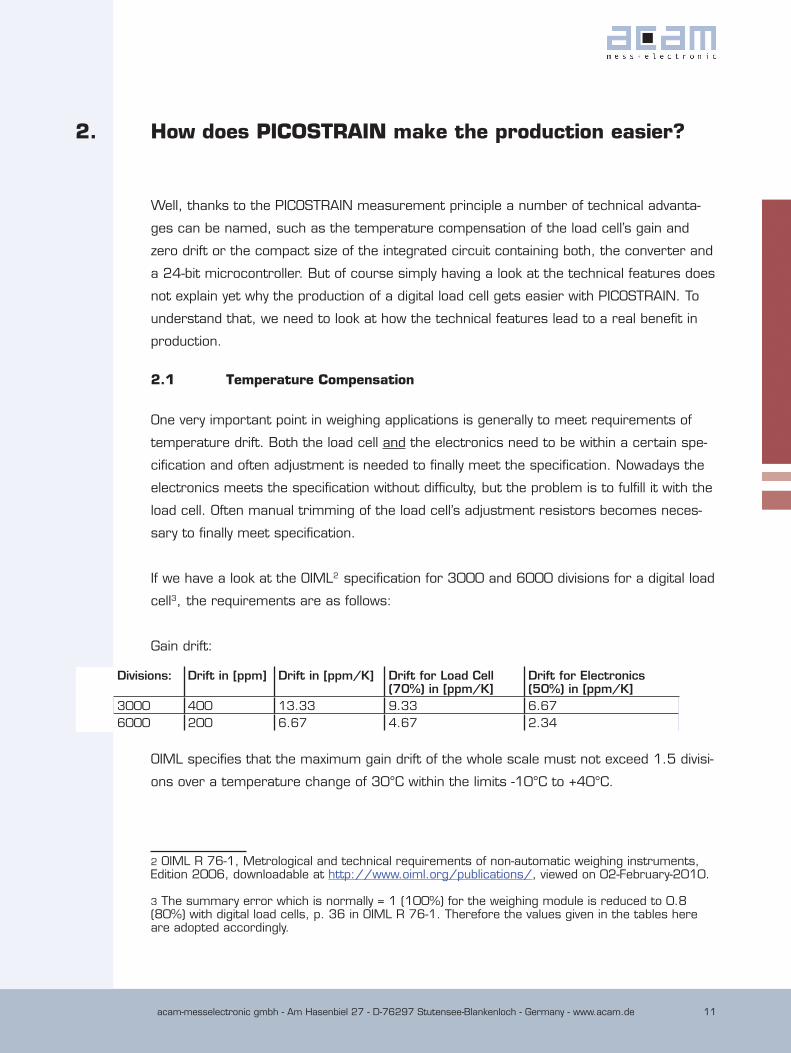
2.1 Temperature Compensation
One very important point in weighing applications is generally to meet requirements of
temperature drift. Both the load cell and the electronics need to be within a certain spe-
cification and often adjustment is needed to finally meet the specification. Nowadays the
electronics meets the specification without difficulty, but the problem is to fulfill it with the
load cell. Often manual trimming of the load cell’s adjustment resistors becomes neces-
sary to finally meet specification.
If we have a look at the OIML2 specification for 3000 and 6000 divisions for a digital load
cell3, the requirements are as follows:
Gain drift:
OIML specifies that the maximum gain drift of the whole scale must not exceed 1.5 divisi-
ons over a temperature change of 30°C within the limits -10°C to +40°C.
2 OIML R 76-1, Metrological and technical requirements of non-automatic weighing instruments, Edition 2006, downloadable at http://www.oiml.org/publications/, viewed on 02-February-2010.
3 The summary error which is normally = 1 (100%) for the weighing module is reduced to 0.8 (80%) with digital load cells, p. 36 in OIML R 76-1. Therefore the values given in the tables here are adopted accordingly.
Divisions: Drift in [ppm] Drift in [ppm/K] Drift for Load Cell (70%) in [ppm/K]
Drift for Electronics (50%) in [ppm/K]
3000 400 13.33 9.33 6.676000 200 6.67 4.67 2.34
acam-messelectronic gmbh - Am Hasenbiel 27 - D-76297 Stutensee-Blankenloch - Germany - www.acam.de12
1®
acam-messelectronic gmbh - Am Hasenbiel 27 - D-76297 Stutensee-Blankenloch - Germany - www.acam.de12
2.
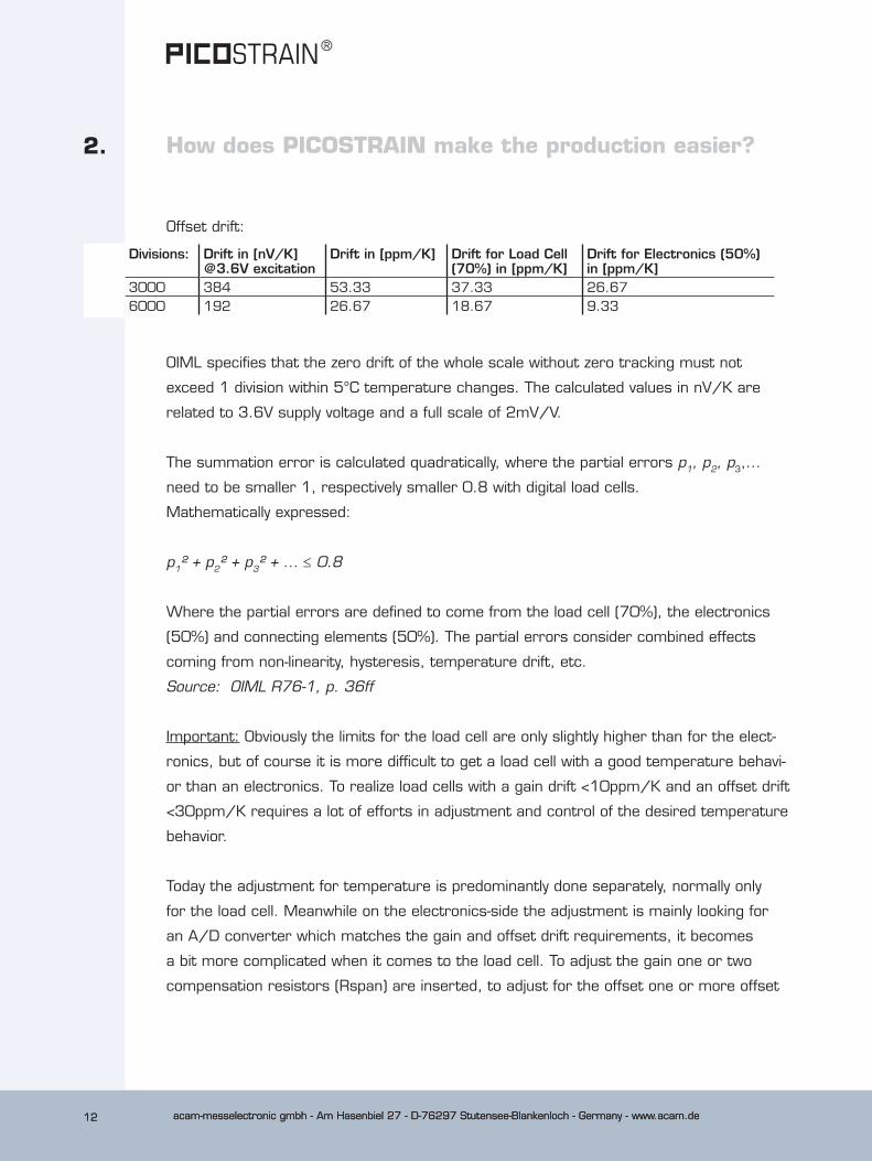
Offset drift:
How does PICOSTRAIN make the production easier?
Divisions: Drift in [nV/K]@3.6V excitation
Drift in [ppm/K] Drift for Load Cell (70%) in [ppm/K]
Drift for Electronics (50%)in [ppm/K]
3000 384 53.33 37.33 26.676000 192 26.67 18.67 9.33
OIML specifies that the zero drift of the whole scale without zero tracking must not
exceed 1 division within 5°C temperature changes. The calculated values in nV/K are
related to 3.6V supply voltage and a full scale of 2mV/V.
The summation error is calculated quadratically, where the partial errors p1, p2, p3,...
need to be smaller 1, respectively smaller 0.8 with digital load cells.
Mathematically expressed:
p1² + p2² + p3² + ... ≤ 0.8
Where the partial errors are defined to come from the load cell (70%), the electronics
(50%) and connecting elements (50%). The partial errors consider combined effects
coming from non-linearity, hysteresis, temperature drift, etc.
Source: OIML R76-1, p. 36ff
Important: Obviously the limits for the load cell are only slightly higher than for the elect-
ronics, but of course it is more difficult to get a load cell with a good temperature behavi-
or than an electronics. To realize load cells with a gain drift <10ppm/K and an offset drift
<30ppm/K requires a lot of efforts in adjustment and control of the desired temperature
behavior.
Today the adjustment for temperature is predominantly done separately, normally only
for the load cell. Meanwhile on the electronics-side the adjustment is mainly looking for
an A/D converter which matches the gain and offset drift requirements, it becomes
a bit more complicated when it comes to the load cell. To adjust the gain one or two
compensation resistors (Rspan) are inserted, to adjust for the offset one or more offset

acam-messelectronic gmbh - Am Hasenbiel 27 - D-76297 Stutensee-Blankenloch - Germany - www.acam.de 13acam-messelectronic gmbh - Am Hasenbiel 27 - D-76297 Stutensee-Blankenloch - Germany - www.acam.de 13
2.
adjustment resistors are added. A circuitry of the load cell strain gage sensors with the
needed adjustment resistors looks like the following:
How does PICOSTRAIN make the production easier?
Fig. 4: Classical Wheatstone-bridge with Adjustment Resistors
Expressed in other words:Today’s load cell adjustment for gain and offset drift is a method of an iterative
adjustment which is manually performed on the basis of experience.
The size of Rspan and Roff can only be estimated to compensate for the drift of the
strain gage resistors in the first approach. After testing gain and offset drift in the tem-
perature chamber, corrections to both are made. These corrections are done manually
by hand and according to the knowledge and experience of the load cell manufacturer. It
sometimes takes more than one control run to get the desired behavior at the end.
acam-messelectronic gmbh - Am Hasenbiel 27 - D-76297 Stutensee-Blankenloch - Germany - www.acam.de14
1®
acam-messelectronic gmbh - Am Hasenbiel 27 - D-76297 Stutensee-Blankenloch - Germany - www.acam.de14
2.
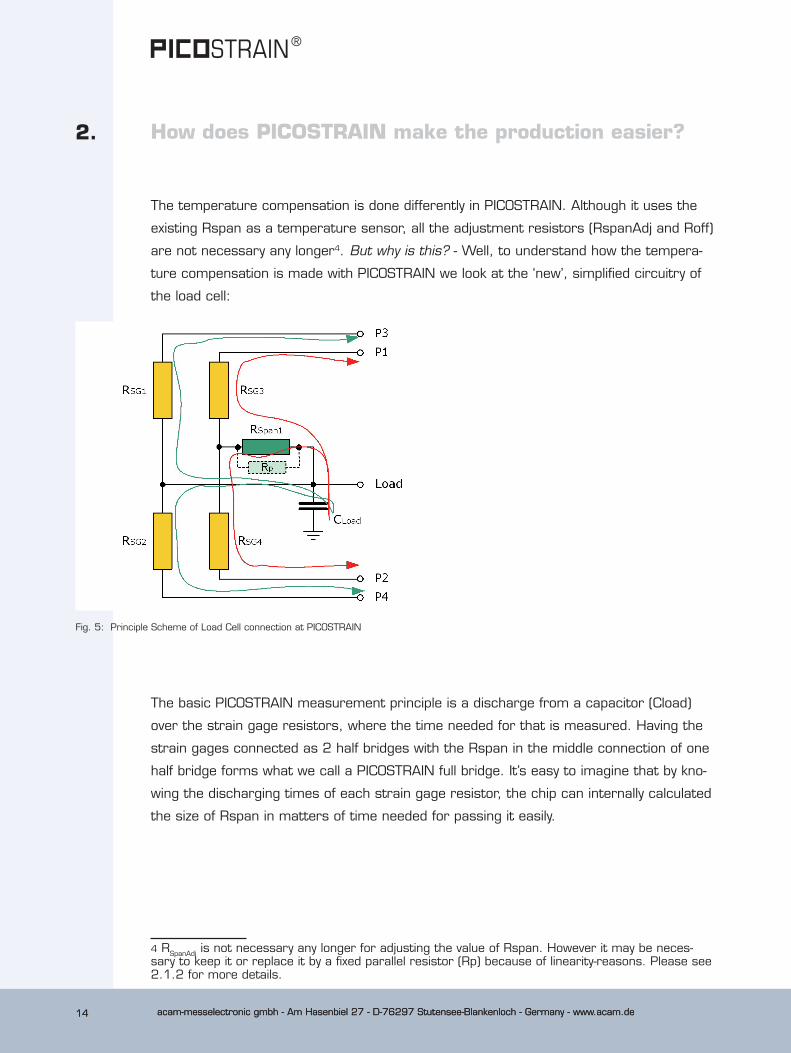
The temperature compensation is done differently in PICOSTRAIN. Although it uses the
existing Rspan as a temperature sensor, all the adjustment resistors (RspanAdj and Roff)
are not necessary any longer4. But why is this? - Well, to understand how the tempera-
ture compensation is made with PICOSTRAIN we look at the ‘new’, simplified circuitry of
the load cell:
The basic PICOSTRAIN measurement principle is a discharge from a capacitor (Cload)
over the strain gage resistors, where the time needed for that is measured. Having the
strain gages connected as 2 half bridges with the Rspan in the middle connection of one
half bridge forms what we call a PICOSTRAIN full bridge. It’s easy to imagine that by kno-
wing the discharging times of each strain gage resistor, the chip can internally calculated
the size of Rspan in matters of time needed for passing it easily.
4 RSpanAdj is not necessary any longer for adjusting the value of Rspan. However it may be neces-sary to keep it or replace it by a fixed parallel resistor (Rp) because of linearity-reasons. Please see 2.1.2 for more details.
How does PICOSTRAIN make the production easier?
Fig. 5: Principle Scheme of Load Cell connection at PICOSTRAIN

acam-messelectronic gmbh - Am Hasenbiel 27 - D-76297 Stutensee-Blankenloch - Germany - www.acam.de 15acam-messelectronic gmbh - Am Hasenbiel 27 - D-76297 Stutensee-Blankenloch - Germany - www.acam.de 15
2.
Fig. 6: Determining time tr needed to pass Rspan
In other words, the PICOSTRAIN chips have more information about each and every
resistor of the load cell circuitry as the A/D converter has with the Wheatstone-bridge
which only measures the differential voltage. With this ‘more of information’ the chip can
of course multiply the time interval measured for Rspan internally and also know and re-
member the offset between the two half bridges. At this point it is an advantage to have
not only the converter but also the microcontroller inside, which can handle all calculati-
ons needed, i.e. in this case subtracting the offset.
To adjust for the gain and offset drift there is only one temperature run needed to find
out the corresponding correction factors (they are called TGain and TKOffset). As no
manual correction by hand is needed the whole adjustment process can be done with the
finally produced load cell. The adjustment process needs less time and is very accurate.
A detailed description of how to determine the correction factors and what results can
be achieved, please have a look at our White Paper #002 „How to Lower the Gain and
Offset Drift of a Load Cell“.
How does PICOSTRAIN make the production easier?
Conclusion:
The temperature compensation is done in a different way at PICOSTRAIN. It reduces
the needed components and makes the adjustment easier and faster. Instead of making
several iterations to finally meet specifications normally one single temperature run is
sufficient. More than that, the whole adjustment procedure can be fully automated.
The principle is illustrated in the next figure:

acam-messelectronic gmbh - Am Hasenbiel 27 - D-76297 Stutensee-Blankenloch - Germany - www.acam.de16
1®
acam-messelectronic gmbh - Am Hasenbiel 27 - D-76297 Stutensee-Blankenloch - Germany - www.acam.de16
2. How does PICOSTRAIN make the production easier?
2.1.1 Compensation resistor Rspan
PICOSTRAIN needs only one Rspan resistor. As the Common Mode Rejection Ratio
(CMRR) of the PICOSTRAIN products is nearly infinite (up to 135dB !), there is no need
to use two Rspan resistors. Indeed, PICOSTRAIN can not handle bridges with two Rspan
resistors. However there are ways to connect two Rspans on the load cell to only one or
by simply short-cutting one first tests can be made.
Generally, using an Rspan resistor is a powerful way to get a good gain and offset drift
compensation of the load cell. The resistor’s value for a 350Ω load cell is normally in the
range from 39Ω to 47Ω, for a 1kΩ load cell it may be in the range from 100Ω to 120Ω.
In practice an Rspan resistor of fixed value is chosen roughly to compensate for the
change in sensitivity over temperature. The fine adjustment is then done by another resis-
tor (RSpanAdj) which lies in parallel to Rspan, normally placed on the connection field. This
mechanical trimming becomes unnecessary with PICOSTRAIN. We can multiply Rspan in
a wide range and with a very high precision to adjust it to the desired value.
The Rspan is normally placed on the load cell to give a maximum of temperature coupling
between the load cell body, the strain gage resistors and Rspan. This way, Rspan can
react fast and accurate to temperature changes. However there is a good alternative
for the placement of Rspan when it comes to the digital load cell. It can be placed on
the PCB in the connection field, this is possible as the PCB is directly on the load cell so
that there is also a good thermal coupling, too. As it is not necessary to adjust Rspan
mechanically, you can choose Rspan from a wide range of values and multiply it by the
PICOSTRAIN method to the needed value. More than that, the Rspan can consist of a
standard Nickel or Platinum resistor in a standard housing, such as SMD 603. This way,
costs can be reduced and it also simplifies the set-up of the load cell. The four strain
Please note: The multiplication factor for Rspan (called TKGain) can be choosen from 0.0
to 7.99 with 24-Bit accuracy.
Example: With TKGain you can multiply a 39Ω resistor from 0.0Ω up to 312Ω with a
minimum step size of 0.59 mΩ. An absolutly high end resistor with 0.01% accuracy has
a value missmatch of 3.9 mOhm at 39 Ohm or 6-times less accurate than the multiplica-
tion accuracy of TkGain.
acam-messelectronic gmbh - Am Hasenbiel 27 - D-76297 Stutensee-Blankenloch - Germany - www.acam.de 17acam-messelectronic gmbh - Am Hasenbiel 27 - D-76297 Stutensee-Blankenloch - Germany - www.acam.de 17
2. How does PICOSTRAIN make the production easier?
gage resistors do not change, also the adjustment procedure in the PICOSTRAIN way
does not change, it works fine as long as there is one Rspan connected no matter where
it is placed.
Of course the results with an Rspan placed on the load cell body as usually will give best
results. On the other hand, the requirements of legal specifications like OIML do not
focus on fast thermal reaction (there is a settling time of 2 hours!) so that the proposed
alternative is a nice possibility to reduce costs for standard legal for trade load cells (C3).
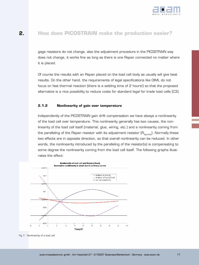
2.1.2 Nonlinearity of gain over temperature
Independently of the PICOSTRAIN gain drift compensation we have always a nonlinearity
of the load cell over temperature. This nonlinearity generally has two causes, the non-
linearity of the load cell itself (material, glue, wiring, etc.) and a nonlinearity coming from
the paralleling of the Rspan resistor with its adjustment resistor (RSpanAdj). Normally these
two effects are in opposite direction, so that overall nonlinearity can be reduced. In other
words, the nonlinearity introduced by the paralleling of the resistor(s) is compensating to
some degree the nonlinearity coming from the load cell itself. The following graphs illust-
rates the effect:
Fig 7: Nonlinearity of a load cell
acam-messelectronic gmbh - Am Hasenbiel 27 - D-76297 Stutensee-Blankenloch - Germany - www.acam.de18
1®
acam-messelectronic gmbh - Am Hasenbiel 27 - D-76297 Stutensee-Blankenloch - Germany - www.acam.de18
2. How does PICOSTRAIN make the production easier?
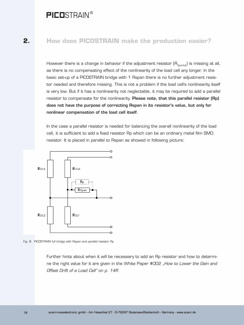
However there is a change in behavior if the adjustment resistor (RSpanAdj) is missing at all,
as there is no compensating effect of the nonlinearity of the load cell any longer. In the
basic set-up of a PICOSTRAIN bridge with 1 Rspan there is no further adjustment resis-
tor needed and therefore missing. This is not a problem if the load cell’s nonlinearity itself
is very low. But if it has a nonlinearity not neglectable, it may be required to add a parallel
resistor to compensate for the nonlinearity. Please note, that this parallel resistor (Rp)
does not have the purpose of correcting Rspan in its resistor’s value, but only for
nonlinear compensation of the load cell itself.
In the case a parallel resistor is needed for balancing the overall nonlinearity of the load
cell, it is sufficient to add a fixed resistor Rp which can be an ordinary metal film SMD
resistor. It is placed in parallel to Rspan as showed in following picture:
Fig. 8: PICOSTRAIN full bridge with Rspan and parallel resistor Rp
Further hints about when it will be necessary to add an Rp resistor and how to determi-
ne the right value for it are given in the White Paper #002 „How to Lower the Gain and
Offset Drift of a Load Cell“ on p. 14ff.
acam-messelectronic gmbh - Am Hasenbiel 27 - D-76297 Stutensee-Blankenloch - Germany - www.acam.de 19acam-messelectronic gmbh - Am Hasenbiel 27 - D-76297 Stutensee-Blankenloch - Germany - www.acam.de 19
2. How does PICOSTRAIN make the production easier?
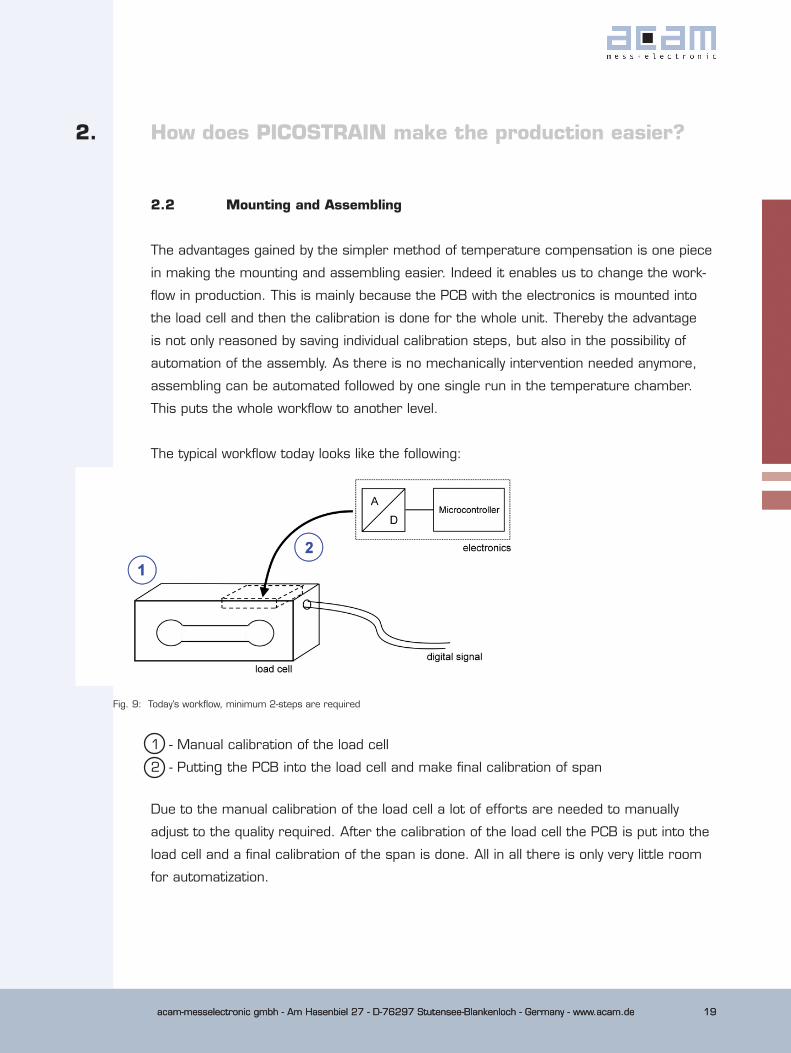
2.2 Mounting and Assembling
The advantages gained by the simpler method of temperature compensation is one piece
in making the mounting and assembling easier. Indeed it enables us to change the work-
flow in production. This is mainly because the PCB with the electronics is mounted into
the load cell and then the calibration is done for the whole unit. Thereby the advantage
is not only reasoned by saving individual calibration steps, but also in the possibility of
automation of the assembly. As there is no mechanically intervention needed anymore,
assembling can be automated followed by one single run in the temperature chamber.
This puts the whole workflow to another level.
The typical workflow today looks like the following:
Fig. 9: Today’s workflow, minimum 2-steps are required
1 - Manual calibration of the load cell
2 - Putting the PCB into the load cell and make final calibration of span
Due to the manual calibration of the load cell a lot of efforts are needed to manually
adjust to the quality required. After the calibration of the load cell the PCB is put into the
load cell and a final calibration of the span is done. All in all there is only very little room
for automatization.

acam-messelectronic gmbh - Am Hasenbiel 27 - D-76297 Stutensee-Blankenloch - Germany - www.acam.de20
1®
acam-messelectronic gmbh - Am Hasenbiel 27 - D-76297 Stutensee-Blankenloch - Germany - www.acam.de20
2. How does PICOSTRAIN make the production easier?
PICOSTRAIN on the contrary works different – the electronics can be mounted first and
then the adjustment is done for the whole unit. This way processing steps are saved
and the adjustment made much easier. The following picture illustrated the new possible
workflow:
Fig. 10: 1-step workflow possible with PICOSTRAIN
Beneficial to this approach is also the fact that we do not need the converter and micro-
processor separately, but they are united in one single chip. Furthermore, the chip size is
quite small with a Die-size of 3.47x2.37mm or as QFN56 with 7x7mm. This way, we can
lay out a very compact PCB only containing a very few components so that overall size
can be reduced to a minimum.
Summarized, the benefits of this new and simpler approach are as follows:
� All the calibration is done at once and can be fully automated
� Only 1 compensation resistor (Rspan) is needed instead of normally 4-6 adjustment
resistors
� The load cell can be completely assembled before adjustment procedure
� A gain an offset drift which lies deeply within legal specifications like OIML
Especially the latter is a benefit which automatically comes with the approach to
adjust the wholly mounted system – each component is optimized in gain and off-

acam-messelectronic gmbh - Am Hasenbiel 27 - D-76297 Stutensee-Blankenloch - Germany - www.acam.de 21acam-messelectronic gmbh - Am Hasenbiel 27 - D-76297 Stutensee-Blankenloch - Germany - www.acam.de 21
2. How does PICOSTRAIN make the production easier?
set drift without any additional efforts – and this leads to a superior low gain and
offset drift. In simple words the PICOSTRAIN adjustment brings you automatically
a gain and offset drift behavior which is deeply even within OIML 6000 specifica-
tion. The following values can be reached for a digital load cell (complete unit):
Gain drift: 2ppm/K => 1.7-times better than OIML 6000
Offset drift: 5ppm/K or 35nV/K (at 3.6V)
=> 5.5-times better than OIML 6000
Conclusion:
Based on the different approach of making the temperature compensation, the whole
unit can be assembled before making the correction. This leads to higher automation
and easier adjustment. The number of temperature run cycles is reduced and the whole
workflow optimized. Thereby a rise in quality comes automatically with this approach, gain
and offset drift of the load cell is significantly improved.

acam-messelectronic gmbh - Am Hasenbiel 27 - D-76297 Stutensee-Blankenloch - Germany - www.acam.de22
1®
acam-messelectronic gmbh - Am Hasenbiel 27 - D-76297 Stutensee-Blankenloch - Germany - www.acam.de22
acam-messelectronic gmbh - Am Hasenbiel 27 - D-76297 Stutensee-Blankenloch - Germany - www.acam.de 23
3. Advantages by building a digital load cell with PICOSTRAIN
The benefits outlined in the previous chapter lead to a number of advantages in the
overall application digital load cell. In this section we want to describe the advantages not
only from a technical but also a commercial point of view and have a glance also at the
long-term effects of this approach.
3.1 Cost Saving by Simplified Production
The cost savings by introducing the new work flow can be significant. Besides direct cost
benefits – like having a single chip solution instead of two separate components – there
are several indirect, but nevertheless considerable cost saving factors. Reduced costs
are possible to occur in the following areas due to:
� Reduced number of components, reduced Bill of Material (BOM)
� Smaller PCB size
� Reduced efforts in doing the calibration (no manual adjustment)
� Software compensation replaces manual labor
� Saving (Production-)Time through different workflow
� Rise in quality and reliability without additional expenses
(reach OIML 6000 or more with same efforts needed for OIML 3000!)
Of course changing the production work flow also brings some initial efforts with it.
However, the new work flow will bring significant benefits as outlined above, so that in an
overall view costs can be saved and production made more efficient.
Please see the appendix for the Bill of Material (BOM) of our prototype set-up and also
the compact layout of the corresponding PCB.
3.2 Calibration
The main advantage in regards of calibration is the fact that the wholly mounted unit
(load cell + electronics) can be calibrated at once instead having separately several ite-
rations. Please see for a detailed description the foregoing chapter --> 2.1 Temperature
acam-messelectronic gmbh - Am Hasenbiel 27 - D-76297 Stutensee-Blankenloch - Germany - www.acam.de24
1®
acam-messelectronic gmbh - Am Hasenbiel 27 - D-76297 Stutensee-Blankenloch - Germany - www.acam.de24
3.
Compensation and 2.2 Mounting and Assembling. Calibration is therefore simplified and
can be done faster than in the past. Furthermore it allows to automatize the workflow
and minimize throughput time.
Another aspect of the intrinsically calibration of digital load cells is the consequence for
the use in the field: replacement of a broken load cell gets a lot easier. As the unit itself
is calibrated in production there is no need to calibrate on-site again. The digital load cell
simply can be replaced, the calibration was done before. A good replaceability gets more
and more important nowadays when the customer demands fast service response times.
3.3 Low Current
It may not be required by all kind of digital load cells, but certainly with some of them: a
low current consumption. When it comes to battery driven applications, wireless appli-
cations or portable products, current consumption is an important matter. The PICOS-
TRAIN technology offers at this point an impressing low current consumption compared
to traditional solutions – thanks to its measurement principle.
In a traditional application with the Wheatstone-bridge as sensor the current consumpti-
on with 1kOhm resistors at 5V is according to Ohm’s law 5mA, or 3mA at 3V. Often the
strain gage resistors are 350 Ohm and therefore the current is even higher.
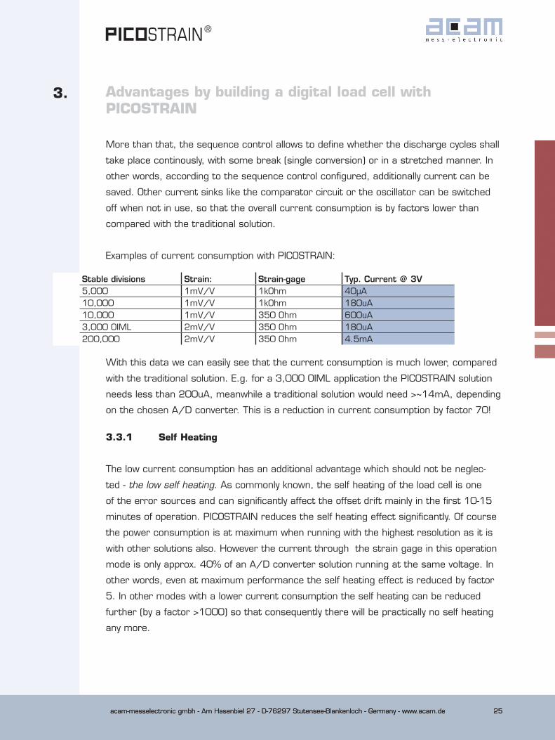
With PICOSTRAIN the strain gage sensors are measured by means of discharge times,
therefore they are driven in a pulsed manner rather than in a continuous manner. Cur-
rent flows into the sensors only during the discharge phase from the capacitor. The capa-
citor itself is recharged in the charging phase , as the following figure shows:
Advantages by building a digital load cell with PICOSTRAIN
Fig. 11: Current during charge phase of capacitor
acam-messelectronic gmbh - Am Hasenbiel 27 - D-76297 Stutensee-Blankenloch - Germany - www.acam.de 25acam-messelectronic gmbh - Am Hasenbiel 27 - D-76297 Stutensee-Blankenloch - Germany - www.acam.de 25
1®
3.
More than that, the sequence control allows to define whether the discharge cycles shall
take place continously, with some break (single conversion) or in a stretched manner. In
other words, according to the sequence control configured, additionally current can be
saved. Other current sinks like the comparator circuit or the oscillator can be switched
off when not in use, so that the overall current consumption is by factors lower than
compared with the traditional solution.
Examples of current consumption with PICOSTRAIN:
Advantages by building a digital load cell with PICOSTRAIN
Stable divisions Strain: Strain-gage Typ. Current @ 3V5,000 1mV/V 1kOhm 40µA10,000 1mV/V 1kOhm 180uA10,000 1mV/V 350 Ohm 600uA3,000 OIML 2mV/V 350 Ohm 180uA200,000 2mV/V 350 Ohm 4.5mA
With this data we can easily see that the current consumption is much lower, compared
with the traditional solution. E.g. for a 3,000 OIML application the PICOSTRAIN solution
needs less than 200uA, meanwhile a traditional solution would need >~14mA, depending
on the chosen A/D converter. This is a reduction in current consumption by factor 70!
3.3.1 Self Heating
The low current consumption has an additional advantage which should not be neglec-
ted - the low self heating. As commonly known, the self heating of the load cell is one
of the error sources and can significantly affect the offset drift mainly in the first 10-15
minutes of operation. PICOSTRAIN reduces the self heating effect significantly. Of course
the power consumption is at maximum when running with the highest resolution as it is
with other solutions also. However the current through the strain gage in this operation
mode is only approx. 40% of an A/D converter solution running at the same voltage. In
other words, even at maximum performance the self heating effect is reduced by factor
5. In other modes with a lower current consumption the self heating can be reduced
further (by a factor >1000) so that consequently there will be practically no self heating
any more.
acam-messelectronic gmbh - Am Hasenbiel 27 - D-76297 Stutensee-Blankenloch - Germany - www.acam.de26
1®
acam-messelectronic gmbh - Am Hasenbiel 27 - D-76297 Stutensee-Blankenloch - Germany - www.acam.de26
3. Advantages by building a digital load cell with PICOSTRAIN
3.4 EMI behavior
The question of a good electromagnetically interference behavior (EMI) is omnipresent in
the scale world of today. Often a lot of efforts (and time) are spend to meet EMI specifi-
cations and a lot of try-and-error cycles are often needed to optimize the design. Since
January 2010 the even more strict OIML regulation R76-1 (from 2006)5 is active which
requires electromagnetically conformity (EMC) to 10V/m instead of formerly 3V/m, so it
will get significantly more difficult to match the new specification.
Fortunately also in this area the concept of a digital load cell can play out its strength.
Thanks to the nature of the digital load cell some points appear less critical compared to
an ordinary scale set-up. For example, the wire length in total is much shorter then with
a normal scale and the digitalization of the value happens shortly after the sensor. So
there is not much way for the transmission of the analog signal, which basically reduces
the critical path where interference can occur.
The second advantage we have with a digital load cell set up is the housing. When the
PCB is put into the body of the load cell (normally aluminium or steel), it is acting as a
shield for the electronics. In other words, the encapsulation is very good and electro-
magnetical interference is reduced significantly.
Because of this constructional advantages it is quite good feasible to reach immunity
against the required strength level of 10 V/m (80 MHz to 2 GHz). This saves time and
cost in development.
5 International OIML recommendations according to PTB (Physikalisch-Technische Bundesanstalt, German National Metrology Institute in Braunschweig and Berlin). <http://www.ptb.de/en/org/1/11/112/_index.htm>, viewed on 02-February-2010.OIML R 76-1, Metrological and technical requirements of non-automatic weighing instruments, Edi-tion 2006, downloadable at <http://www.oiml.org/publications/>, viewed on 02-February-2010.
acam-messelectronic gmbh - Am Hasenbiel 27 - D-76297 Stutensee-Blankenloch - Germany - www.acam.de 27acam-messelectronic gmbh - Am Hasenbiel 27 - D-76297 Stutensee-Blankenloch - Germany - www.acam.de 27
1®
3.
3.5 Commercial aspects
Finally we want to have a look at the commercial aspects of a digital load cell (produc-
tion). As introductorily mentioned, today the digital load cell is still a niche product which
cannot reach the sales figures of its analog correspondent due to high efforts in both
time and costs in production. More than that, there is only a small chance to automatize
the production with today’s workflow, so costs cannot be reduced.
Another cost driving factor is the number of components needed to build the
nowadays electronics. There is not only the fact that two chips are needed
(converter+microcontroller) but also supportive components like an EEPROM are needed.
In other words, the Bill of Material (BOM) is relatively long and can not be reduced by
easy measures.
In contrary to the current possible solutions we have with PICOSTRAIN some advantages
which potentially lead to a reduction of cost and less elaborate production. As described
in detail in the previous chapters the workflow can be changed, temperature calibrati-
on will be easier and the number of needed components is significantly reduced. This
altogether with the fact that this new workflow enables you to use a higher degree of
automatization leads to a potentially cost saving production. We really would like to give
an example here, e.g. how much money you can save on each produced load cell or how
labour and machine expenses can be lowered.
But of course such an estimation cannot be serious, as we are firstly not a load cell ma-
nufacturer and secondly you all know that labour and machine expenses differ significantly
around the world. In other words how much money you will save depends on where your
production is located and to which degree you are going to automate the production. So
the cost saving will be individually different for each manufacturer respectively production.
What we want to point out here is that the potential for saving cost is definitely given and
just depends on to which degree you exploit it to.
Advantages by building a digital load cell with PICOSTRAIN

acam-messelectronic gmbh - Am Hasenbiel 27 - D-76297 Stutensee-Blankenloch - Germany - www.acam.de28
1®
acam-messelectronic gmbh - Am Hasenbiel 27 - D-76297 Stutensee-Blankenloch - Germany - www.acam.de28
3.
3.6 Digital Load Cells in Standard Scales
Nowadays digital load cells are still only used in special applications like truck scales, silo
scales, container scales, etc. In common standard scales like i.e. bench scales or legal
for trade scales they are not used very often.
But exactly in this area there is a lot of benefit in using DLCs, some advantages cannot
be realized by using the analog load cell. The idea of a new possible structure is illustra-
ted in the following picture:
Fig. 12: Separation of analog (weighing) part and the digital part
In this structure the weighing part is separated from the pure digital part handling input/
output functions. The tasks fullfilled by each part can be defined as follows:
Advantages by building a digital load cell with PICOSTRAIN
acam-messelectronic gmbh - Am Hasenbiel 27 - D-76297 Stutensee-Blankenloch - Germany - www.acam.de 29acam-messelectronic gmbh - Am Hasenbiel 27 - D-76297 Stutensee-Blankenloch - Germany - www.acam.de 29
1®
3.
High end analog part Pure digital part � Consisting of load cell and the weighing
electronics
� Weighing know-how required
� Output is a digital data stream
� Results already fully calibrated, linearized,
temperature compensated, etc.
� Meet legal specifications like OIML
� Consisting of pure digital PCB
� Handling input/output like buttons, LCD or
further interfaces
� May contain further software for language
localization etc.
� No weighing know-how required
The analog part includes the sensor (load cell) and the electronic. The knowledge about
weighing lies in this part, i.e. construction of a good load cell or to make calibration, tem-
perature compensation, etc. The output is fully digital signal which delivers the weighing
information already fully calibrated.
The pure digital part on the other hand receives the digital data stream and just handles
tasks like displaying of the weight, recognition of buttons or interface other devices (e.g.
network scales). Also, language or country localization can be done in the software here.
To make the digital part there is not much knowledge about weighing itself needed.
You may ask what this could be good for? - Well, there are a number of advantages of
this approach, such as:
� The PCBs can be designed especially for their purpose. The PCB of the analog part
usually has different requirements to the digital part. E.g. instead of having 1 large
PCB consisting of 4-layers, may only the analog part (small PCB) have 4-layers but the
digital (larger PCB) only 2-layers.
� The high end analog PCB can be re-used in many load cells. Changes in the design of
the scale do not affect the load cell this way. Development efforts are reduced.
� Development work can be divided and transfered to different persons. The designer
who does the digital part does not necessarily need knowledge about (the more com-
plex) weighing technology.
� EMI conformance can be achieved easier as the measurement values are digitized at
a very early stage and due to the good encapsulation of the PCB.
Advantages by building a digital load cell with PICOSTRAIN
acam-messelectronic gmbh - Am Hasenbiel 27 - D-76297 Stutensee-Blankenloch - Germany - www.acam.de30
1®
acam-messelectronic gmbh - Am Hasenbiel 27 - D-76297 Stutensee-Blankenloch - Germany - www.acam.de30
3.
To connect the two parts a simple SPI protocol is used. This is widely available in almost
every microcontroller and easy to connect. Typical lengths of 3-4m is no problem for this
interface and sufficient for most application in consideration.
Conclusion:
In conclusion of this chapter we see that the concept of building a digital load cell with
PICOSTRAIN does not only have several technical advantages but also commercial ones.
A way to produce high quality digital load cells with a moderate effort and therefore costs
is available now. Additional advantages in regards of low current consumption, better EMI
behavior and new concepts for ordinary standards scales were pointed out.
Advantages by building a digital load cell with PICOSTRAIN
acam-messelectronic gmbh - Am Hasenbiel 27 - D-76297 Stutensee-Blankenloch - Germany - www.acam.de 31
4. Prototype
In the first quarter of 2010 acam built up several prototypes of a digital load cell. The
goal was to investigate if a set-up like we imagined it was feasible and how the results
would be in regards of resolution, temperature behavior, current consumption, etc. For
this purpose we took a standard C3 load cell (the same as we normally use in our PS081
evaluation kit) with the dimensions 130x30x22mm.
In the following section we want to show how we built the prototypes and also show the
results of these investigations.
4.1 Set-Up
The set up encompasses the aspects load cell, PCB and the connection to the computer.
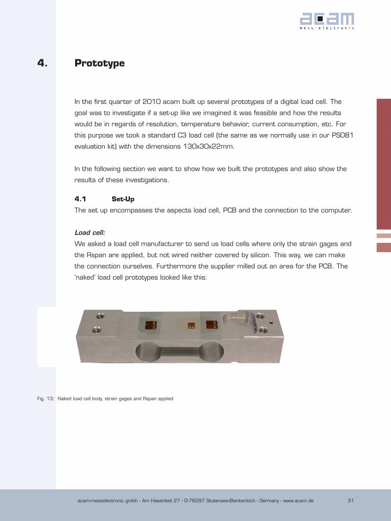
Load cell:
We asked a load cell manufacturer to send us load cells where only the strain gages and
the Rspan are applied, but not wired neither covered by silicon. This way, we can make
the connection ourselves. Furthermore the supplier milled out an area for the PCB. The
‘naked’ load cell prototypes looked like this:
Fig. 13: Naked load cell body, strain gages and Rspan applied
acam-messelectronic gmbh - Am Hasenbiel 27 - D-76297 Stutensee-Blankenloch - Germany - www.acam.de32
1®
acam-messelectronic gmbh - Am Hasenbiel 27 - D-76297 Stutensee-Blankenloch - Germany - www.acam.de32
4. Prototype
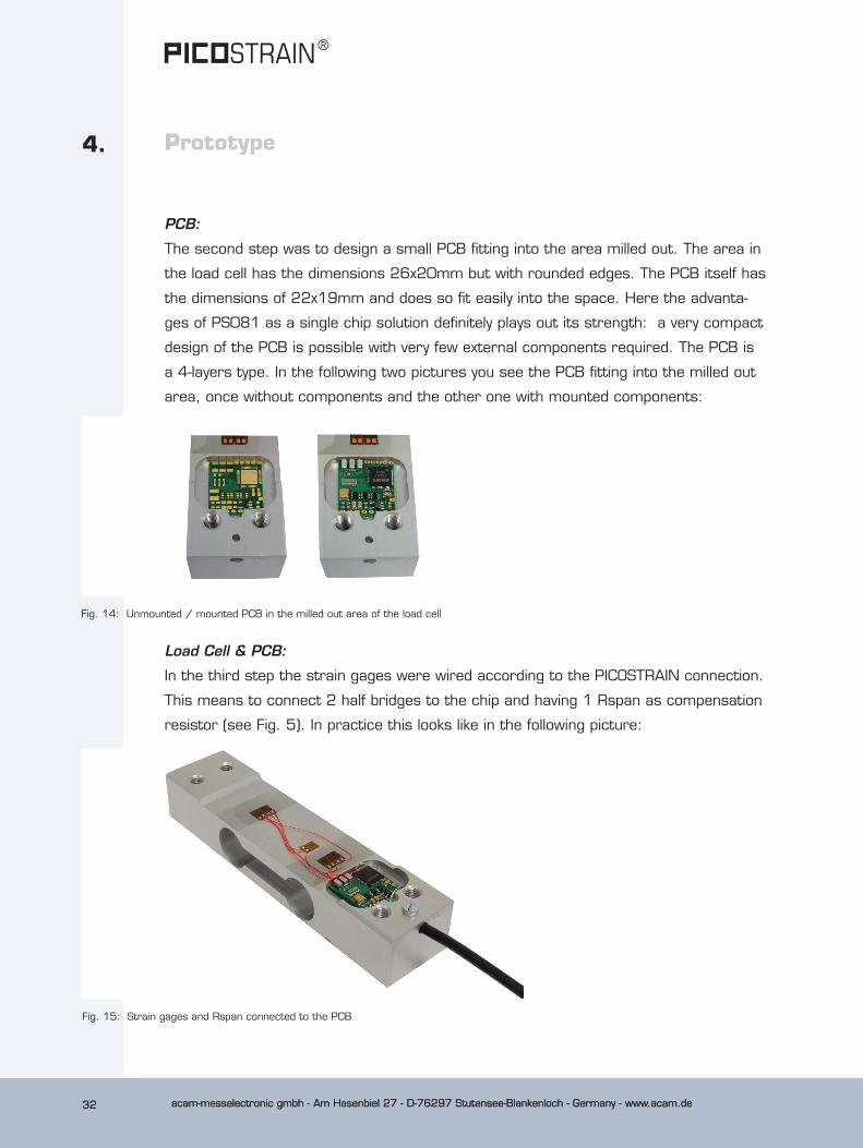
PCB:
The second step was to design a small PCB fitting into the area milled out. The area in
the load cell has the dimensions 26x20mm but with rounded edges. The PCB itself has
the dimensions of 22x19mm and does so fit easily into the space. Here the advanta-
ges of PS081 as a single chip solution definitely plays out its strength: a very compact
design of the PCB is possible with very few external components required. The PCB is
a 4-layers type. In the following two pictures you see the PCB fitting into the milled out
area, once without components and the other one with mounted components:
Fig. 14: Unmounted / mounted PCB in the milled out area of the load cell
Load Cell & PCB:
In the third step the strain gages were wired according to the PICOSTRAIN connection.
This means to connect 2 half bridges to the chip and having 1 Rspan as compensation
resistor (see Fig. 5). In practice this looks like in the following picture:
Fig. 15: Strain gages and Rspan connected to the PCB
acam-messelectronic gmbh - Am Hasenbiel 27 - D-76297 Stutensee-Blankenloch - Germany - www.acam.de 33acam-messelectronic gmbh - Am Hasenbiel 27 - D-76297 Stutensee-Blankenloch - Germany - www.acam.de 33
4. Prototype
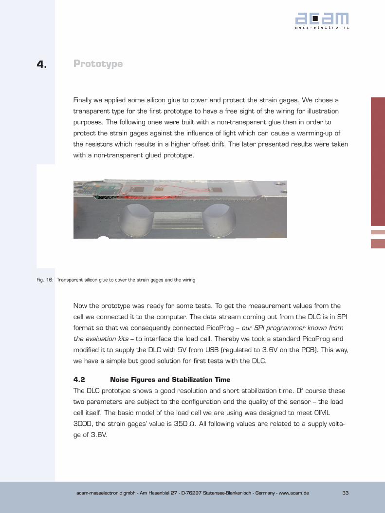
Finally we applied some silicon glue to cover and protect the strain gages. We chose a
transparent type for the first prototype to have a free sight of the wiring for illustration
purposes. The following ones were built with a non-transparent glue then in order to
protect the strain gages against the influence of light which can cause a warming-up of
the resistors which results in a higher offset drift. The later presented results were taken
with a non-transparent glued prototype.
Fig. 16: Transparent silicon glue to cover the strain gages and the wiring
Now the prototype was ready for some tests. To get the measurement values from the
cell we connected it to the computer. The data stream coming out from the DLC is in SPI
format so that we consequently connected PicoProg – our SPI programmer known from
the evaluation kits – to interface the load cell. Thereby we took a standard PicoProg and
modified it to supply the DLC with 5V from USB (regulated to 3.6V on the PCB). This way,
we have a simple but good solution for first tests with the DLC.
4.2 Noise Figures and Stabilization Time
The DLC prototype shows a good resolution and short stabilization time. Of course these
two parameters are subject to the configuration and the quality of the sensor – the load
cell itself. The basic model of the load cell we are using was designed to meet OIML
3000, the strain gages’ value is 350 Ω. All following values are related to a supply volta-
ge of 3.6V.
acam-messelectronic gmbh - Am Hasenbiel 27 - D-76297 Stutensee-Blankenloch - Germany - www.acam.de34
1®
acam-messelectronic gmbh - Am Hasenbiel 27 - D-76297 Stutensee-Blankenloch - Germany - www.acam.de34
4. Prototype
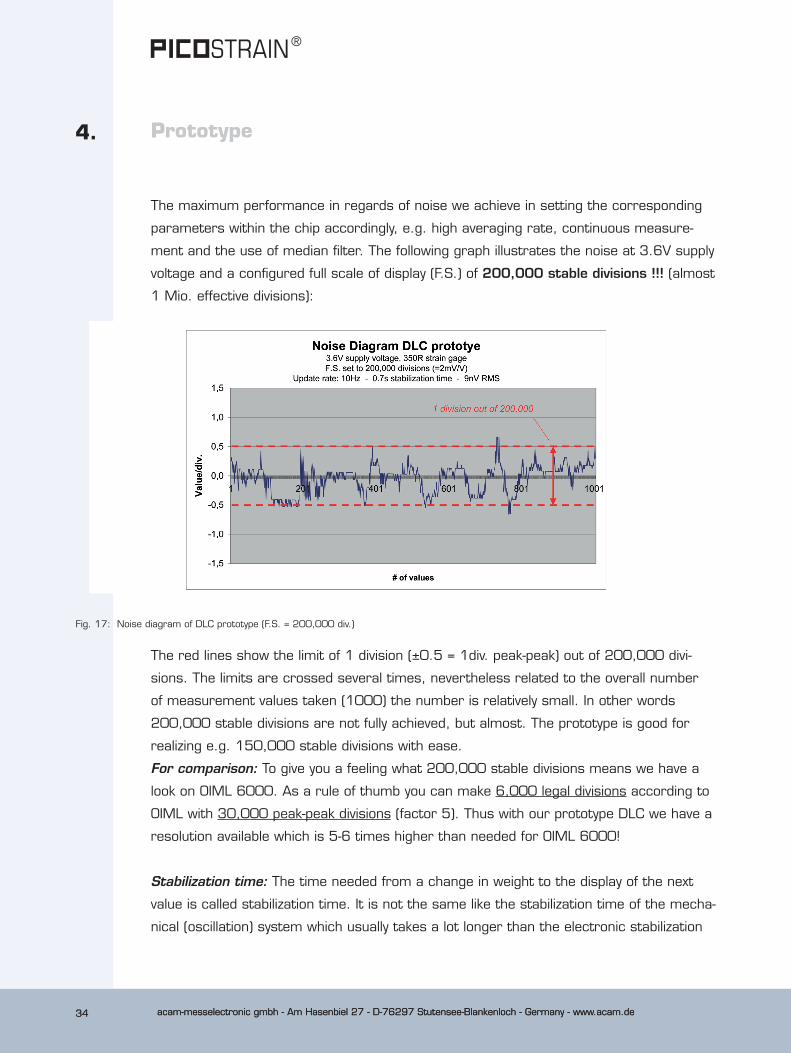
The maximum performance in regards of noise we achieve in setting the corresponding
parameters within the chip accordingly, e.g. high averaging rate, continuous measure-
ment and the use of median filter. The following graph illustrates the noise at 3.6V supply
voltage and a configured full scale of display (F.S.) of 200,000 stable divisions !!! (almost
1 Mio. effective divisions):
Fig. 17: Noise diagram of DLC prototype (F.S. = 200,000 div.)
The red lines show the limit of 1 division (±0.5 = 1div. peak-peak) out of 200,000 divi-
sions. The limits are crossed several times, nevertheless related to the overall number
of measurement values taken (1000) the number is relatively small. In other words
200,000 stable divisions are not fully achieved, but almost. The prototype is good for
realizing e.g. 150,000 stable divisions with ease.
For comparison: To give you a feeling what 200,000 stable divisions means we have a
look on OIML 6000. As a rule of thumb you can make 6,000 legal divisions according to
OIML with 30,000 peak-peak divisions (factor 5). Thus with our prototype DLC we have a
resolution available which is 5-6 times higher than needed for OIML 6000!
Stabilization time: The time needed from a change in weight to the display of the next
value is called stabilization time. It is not the same like the stabilization time of the mecha-
nical (oscillation) system which usually takes a lot longer than the electronic stabilization
acam-messelectronic gmbh - Am Hasenbiel 27 - D-76297 Stutensee-Blankenloch - Germany - www.acam.de 35acam-messelectronic gmbh - Am Hasenbiel 27 - D-76297 Stutensee-Blankenloch - Germany - www.acam.de 35
4. Prototype
time. As the parameters like averaging rate, update rate and filter depth are configura-
ble with PICOSTRAIN you can take influence on the stabilization time. In our prototype
we tried to find an optimum between a good resolution and a short stabilization time – it
is in the range of 0.7 to 0.8 seconds. Shorter stabilization times are also possible but
will result in a lower resolution. For example for a high end OIML load cell you ‘only’ need
30,000 to 60,000 peak-peak divisions instead of 200,000. In this case the stabilization
time of the electronics is as short as <0.3s. This is much shorter than the mechanical
stabilization time of the load cell itself.
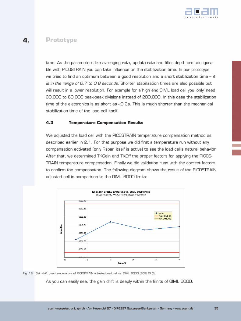
4.3 Temperature Compensation Results
We adjusted the load cell with the PICOSTRAIN temperature compensation method as
described earlier in 2.1. For that purpose we did first a temperature run without any
compensation activated (only Rspan itself is active) to see the load cell’s natural behavior.
After that, we determined TKGain and TKOff the proper factors for applying the PICOS-
TRAIN temperature compensation. Finally we did validation runs with the correct factors
to confirm the compensation. The following diagram shows the result of the PICOSTRAIN
adjusted cell in comparison to the OIML 6000 limits:
Fig. 18: Gain drift over temperature of PICOSTRAIN adjusted load cell vs. OIML 6000 (80% DLC)
As you can easily see, the gain drift is deeply within the limits of OIML 6000.
acam-messelectronic gmbh - Am Hasenbiel 27 - D-76297 Stutensee-Blankenloch - Germany - www.acam.de36
1®
acam-messelectronic gmbh - Am Hasenbiel 27 - D-76297 Stutensee-Blankenloch - Germany - www.acam.de36
4. Prototype
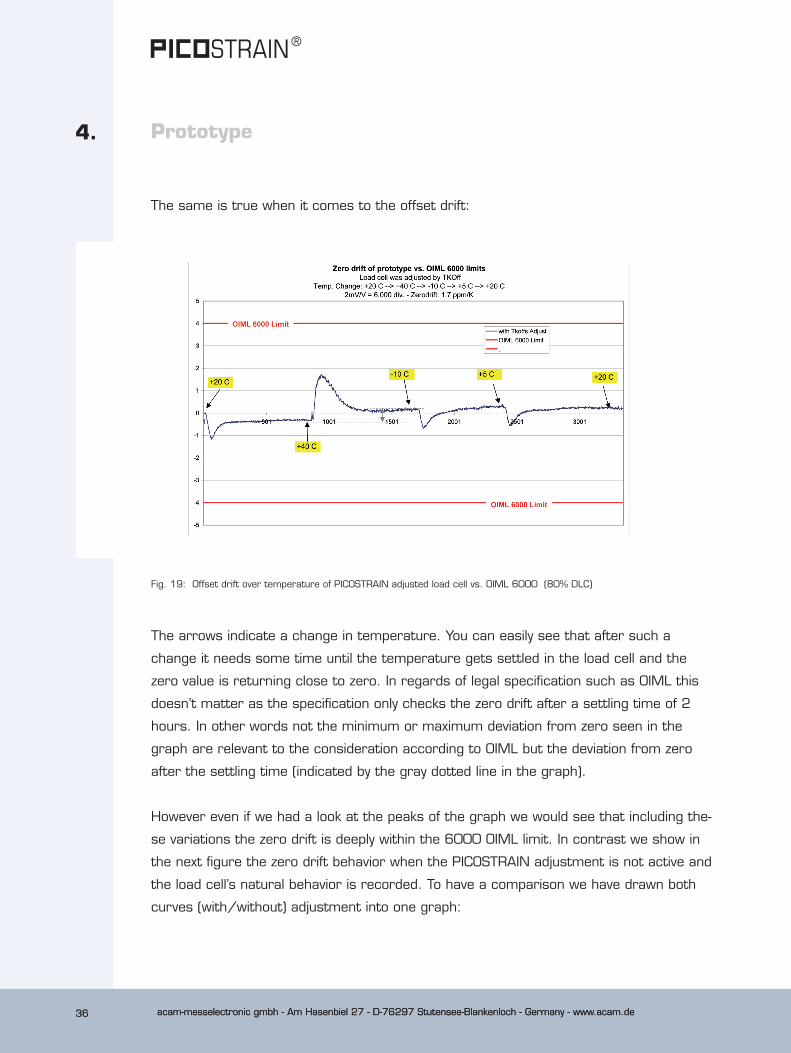
Fig. 19: Offset drift over temperature of PICOSTRAIN adjusted load cell vs. OIML 6000 (80% DLC)
The arrows indicate a change in temperature. You can easily see that after such a
change it needs some time until the temperature gets settled in the load cell and the
zero value is returning close to zero. In regards of legal specification such as OIML this
doesn’t matter as the specification only checks the zero drift after a settling time of 2
hours. In other words not the minimum or maximum deviation from zero seen in the
graph are relevant to the consideration according to OIML but the deviation from zero
after the settling time (indicated by the gray dotted line in the graph).
However even if we had a look at the peaks of the graph we would see that including the-
se variations the zero drift is deeply within the 6000 OIML limit. In contrast we show in
the next figure the zero drift behavior when the PICOSTRAIN adjustment is not active and
the load cell’s natural behavior is recorded. To have a comparison we have drawn both
curves (with/without) adjustment into one graph:
The same is true when it comes to the offset drift:
acam-messelectronic gmbh - Am Hasenbiel 27 - D-76297 Stutensee-Blankenloch - Germany - www.acam.de 37acam-messelectronic gmbh - Am Hasenbiel 27 - D-76297 Stutensee-Blankenloch - Germany - www.acam.de 37
4. Prototype
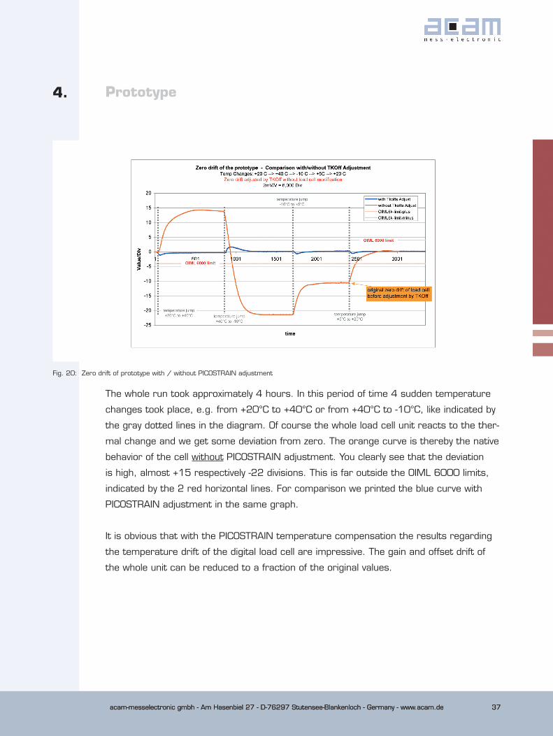
Fig. 20: Zero drift of prototype with / without PICOSTRAIN adjustment
The whole run took approximately 4 hours. In this period of time 4 sudden temperature
changes took place, e.g. from +20°C to +40°C or from +40°C to -10°C, like indicated by
the gray dotted lines in the diagram. Of course the whole load cell unit reacts to the ther-
mal change and we get some deviation from zero. The orange curve is thereby the native
behavior of the cell without PICOSTRAIN adjustment. You clearly see that the deviation
is high, almost +15 respectively -22 divisions. This is far outside the OIML 6000 limits,
indicated by the 2 red horizontal lines. For comparison we printed the blue curve with
PICOSTRAIN adjustment in the same graph.
It is obvious that with the PICOSTRAIN temperature compensation the results regarding
the temperature drift of the digital load cell are impressive. The gain and offset drift of
the whole unit can be reduced to a fraction of the original values.
acam-messelectronic gmbh - Am Hasenbiel 27 - D-76297 Stutensee-Blankenloch - Germany - www.acam.de38
1®
acam-messelectronic gmbh - Am Hasenbiel 27 - D-76297 Stutensee-Blankenloch - Germany - www.acam.de38
4.
4.4 Current Consumption
Thanks to the pulsed measurement principle of PICOSTRAIN current flows only when the
measurement is done. There is no steady current in the bridge required and therefor
overall current consumption can be reduced.
Furthermore the current consumption is related to the configured resolution and stabili-
zation time. The lower the resolution is the lower is also the current consumption. With
the DLC prototype we configured examplarily some typical resolutions and measured the
corresponding current consumption:
Resolution:[peak-peak div.]
Stab. time:[s]
Current Cons.:[mA]
Remarks:
200,0001) 0.7 5.30 Maximum resolution60,0002) 0.7 0.65 Good for OIML 600015,0003) 0.5 0.20 Minimum for OIML 30005,0003) 1.0 0.07 Low current applications
Prototype
1) Continuous Mode 2) Single Conversion Mode 3) Stretched Mode
Please note: There are several modes available in the PICOSTRAIN chips. You can select
continuous measurements or define breaks between measurements to further reduce
the current consumption. The standby current of the prototype is relatively high since the
implemented linear regulator (LDO) has a current consumption of almost ~20µA.
4.5 Interface
The interface of the PICOSTRAIN products is SPI (Serial Peripheral Interface). This full
duplex serial interface bus is a standard protocol in Master/Slave applications. Normally
4 wires are needed to set-up an SPI interface, they are:
SCK (Serial Clock)
SDI (Serial Data In)
SDO (Serial Data Out)
CS/CSN (Chip Select)

acam-messelectronic gmbh - Am Hasenbiel 27 - D-76297 Stutensee-Blankenloch - Germany - www.acam.de 39acam-messelectronic gmbh - Am Hasenbiel 27 - D-76297 Stutensee-Blankenloch - Germany - www.acam.de 39
4.
The typcial clock rate is 1MHz. Details about the timing and the sequence of events of
Read/Write accesses is given in the PS081 data sheet6. An SPI master can collect data
from more than one slave.
The use of this protocol allows easy interconnection between the digital load cell and its
counterpart. In a standard scale this simply can be the connection to the microcontroller
on digital part PCB handling the input and output of data. In a larger scale it can mean
that several DLCs are connected to one central board also interfacing a microcontroller
directly via SPI.
The SPI interface allows connections up to 2-3 m without problems so that most applica-
tions can be served directly by this protocol. However for reasons of protocol conformity
(e.g. RS232) or longer cable lengths another protocol may be chosen. There are several
transceiver chips available (e.g. SPI to RS232) and also a simple microcontroller can do
the job.
Please keep in mind that for the most applications it is absolutely sufficient to connect
them via SPI so we recommend to evaluate properly if you really need to use another
protocol (e.g. in a standard scale you don’t need to use RS232 unless there is a good
technical reason to do so, otherwise you can operate directly via SPI).
4.6 Future Options
The first DLC prototypes were built to see whether it was feasible to use the PICOSTRAIN
benefits in the described set-up or if any unexpected problems occur. As seen in the pre-
vious chapters the results of the first investigations are good. However, further options
may be realized in the future to improve the setup.
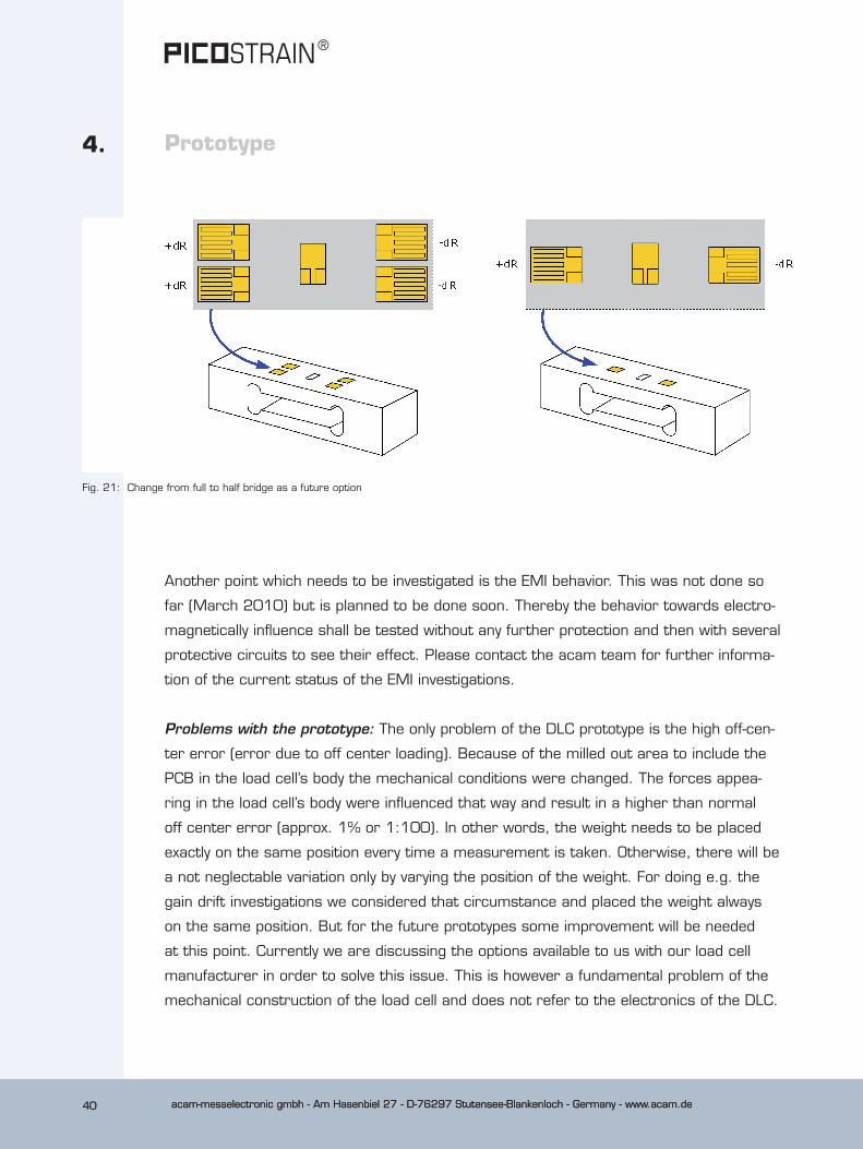
Among them is the possibility to change the full bridge to a half bridge. This option would
save 2 strain gage resistors and therefore further reduce costs. To the PICOSTRAIN
measurement principle it doesn’t matter wheter a half bridge or a full bridge is measu-
red, the measurement quality remains the same (unlike with A/D converter set-ups). The
following pictures illustrate the change:
6 PS081 data sheet (DB-PS081_EN), available at http://www.acam.de/download-section/picos-train.
Prototype
acam-messelectronic gmbh - Am Hasenbiel 27 - D-76297 Stutensee-Blankenloch - Germany - www.acam.de40
1®
acam-messelectronic gmbh - Am Hasenbiel 27 - D-76297 Stutensee-Blankenloch - Germany - www.acam.de40
4. Prototype
Fig. 21: Change from full to half bridge as a future option
Another point which needs to be investigated is the EMI behavior. This was not done so
far (March 2010) but is planned to be done soon. Thereby the behavior towards electro-
magnetically influence shall be tested without any further protection and then with several
protective circuits to see their effect. Please contact the acam team for further informa-
tion of the current status of the EMI investigations.
Problems with the prototype: The only problem of the DLC prototype is the high off-cen-
ter error (error due to off center loading). Because of the milled out area to include the
PCB in the load cell’s body the mechanical conditions were changed. The forces appea-
ring in the load cell’s body were influenced that way and result in a higher than normal
off center error (approx. 1% or 1:100). In other words, the weight needs to be placed
exactly on the same position every time a measurement is taken. Otherwise, there will be
a not neglectable variation only by varying the position of the weight. For doing e.g. the
gain drift investigations we considered that circumstance and placed the weight always
on the same position. But for the future prototypes some improvement will be needed
at this point. Currently we are discussing the options available to us with our load cell
manufacturer in order to solve this issue. This is however a fundamental problem of the
mechanical construction of the load cell and does not refer to the electronics of the DLC.
acam-messelectronic gmbh - Am Hasenbiel 27 - D-76297 Stutensee-Blankenloch - Germany - www.acam.de 41acam-messelectronic gmbh - Am Hasenbiel 27 - D-76297 Stutensee-Blankenloch - Germany - www.acam.de 41
4.
4.7 Conclusion
Prototype
Conclusion:
The DLC prototypes were built up successfully according to the proposed workflow. It was
thereby not only possible to show that it is feasible to build up the digital load cell in “the
PICOSTRAIN way” but also to obtain good first results. Especially the temperature adjust-
ment and the remaining gain and offset drift after adjustment are matching very deeply
legal specifications like OIML 6000. But also the noise figures with resolutions up to
200,000 stable divisions and still short stabilization time are very promising first results.

acam-messelectronic gmbh - Am Hasenbiel 27 - D-76297 Stutensee-Blankenloch - Germany - www.acam.de42
1®
acam-messelectronic gmbh - Am Hasenbiel 27 - D-76297 Stutensee-Blankenloch - Germany - www.acam.de 43
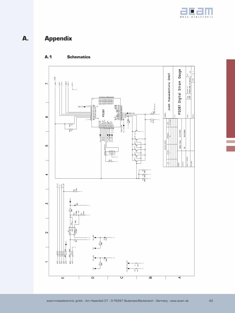
A. Appendix
A.1 Schematics

acam-messelectronic gmbh - Am Hasenbiel 27 - D-76297 Stutensee-Blankenloch - Germany - www.acam.de44
1®
acam-messelectronic gmbh - Am Hasenbiel 27 - D-76297 Stutensee-Blankenloch - Germany - www.acam.de44
A. Appendix
A.2 Layout
Top Layer
GND Layer
Top Assembly
acam-messelectronic gmbh - Am Hasenbiel 27 - D-76297 Stutensee-Blankenloch - Germany - www.acam.de 45acam-messelectronic gmbh - Am Hasenbiel 27 - D-76297 Stutensee-Blankenloch - Germany - www.acam.de 45
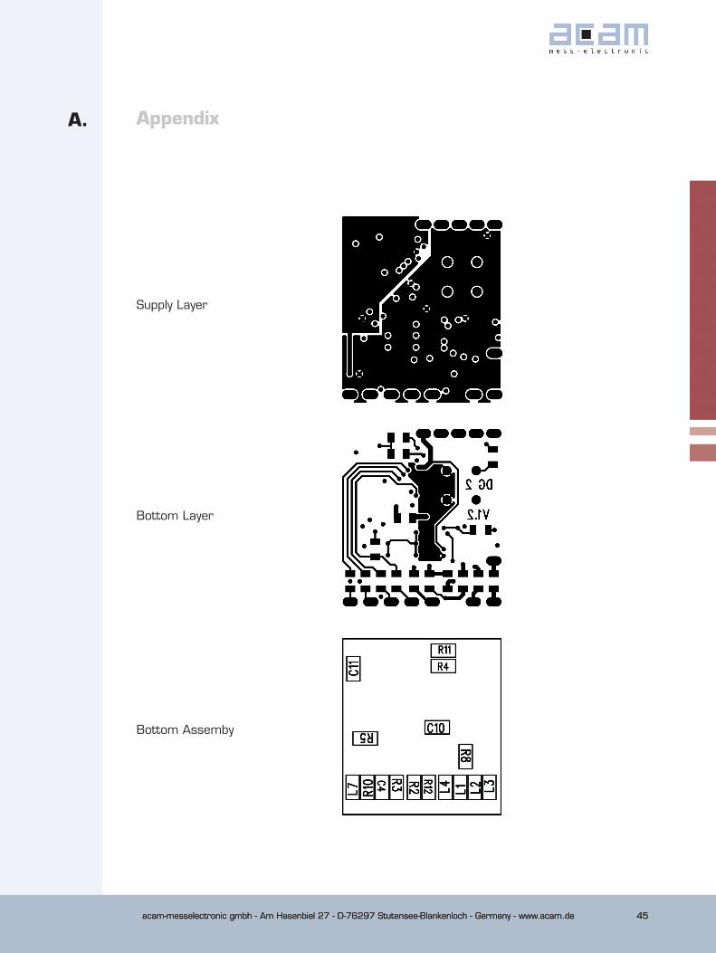
A. Appendix
Supply Layer
Bottom Layer
Bottom Assemby
acam-messelectronic gmbh - Am Hasenbiel 27 - D-76297 Stutensee-Blankenloch - Germany - www.acam.de46
1®
acam-messelectronic gmbh - Am Hasenbiel 27 - D-76297 Stutensee-Blankenloch - Germany - www.acam.de46
A.
A.3 Bill of Material
Qty Reference Value Part Name Description 1 C4 100n C603,100n CHIP-CAPACITOR 1 C3 10u C603,10u CHIP-CAPACITOR 1 C5 3n3 C603,3n3 CHIP-CAPACITOR 2 C10-11 4u7 C603,4u7 CHIP-CAPACITOR 3 C2, C20-21 100n C1206,100n CHIP-CAPACITOR 3 Q4-6 CMKT5087 Double PNP Transistor 5 L1-4, L71 Ferrite 1 C1 220u F95_B,220u Solid Tantalum 3 C6, C14-15 33u F95_P,33u Solid Tantalum 1 U1 LT1761 100mA Low Noise LDO 1 U2 PS081/QFN56 PS081 1 X1 4MHz Q/CSTCR_G,4MHz CERAMIC RESONATOR 1 R8 15k R603,15k CHIP-RESISTOR 1 R9 1M R603,1M CHIP-RESISTOR 1 R3 220k R603,220k CHIP-RESISTOR 3 R1, R10, R12 22R R603,22R CHIP-RESISTOR 2 R6-7 2R2 R603,2R2 CHIP-RESISTOR 1 R5 3k3 R603,3k3 CHIP-RESISTOR 1 R2 430k R603,430k CHIP-RESISTOR 2 R4, R112 CHIP-RESISTOR 1 J1 TESTPOINT2 PAD 12 J2-6 J8-14 TESTPOINT2 Testpoint 2mm1
1 Feritte cores, typically with low DC resitance (e. g. < 0.1R; ≥ 100R@100 MHz)2 This resistor value usually corresponds to the strain gauge resistance
Full Size
Appendix
acam-messelectronic gmbh - Am Hasenbiel 27 - D-76297 Stutensee-Blankenloch - Germany - www.acam.de 47acam-messelectronic gmbh - Am Hasenbiel 27 - D-76297 Stutensee-Blankenloch - Germany - www.acam.de 47
A. Appendix
A.4 Literature Guide
Datasheets
Title Document-No Date
PS081-Single Chip Solution for Strain Gauges
DB_PS081_en V0.5 January 2010
PSØ81-EVA Evaluation System for PSØ81 DB_PS081_EVA V1.0 September 2009
ALCS-350 V2 Load Cell Simulator DB_ALCS_V2 V0.1 August 2009
PicoProg Ø81 DB_PicoProg_Ø81_en_V0.1 January 2010
Whitepapers
Title Document-No Date
How to Lower Gain and Offset Drift Drift of a Load Cell by using TGGain and TKOffset Factors of PSØ81
WP002 V1.0 October 2008
Construction Guideline for solar driven Scales
WP001 V1.0 June 2008
Application Notes
Title Document-No Date
Meterological Investigations of PSØ81 Determining Zero Drift and Gain Drift
AN018 V1.0 July 2008
Strain Gauge Wiring with PICOSTRAIN AN012 V1.0 August 2005
Rspan by Temp CompensationCompensation of Gain error for uncom-pensated Load Cells
AN021 V1.0 July 2009
Design Guidelines for Building a Solar Kitchen Scale
AN022 V1.1 August 2009
Design Guidelines for Building a Solar Body Scale
AN023 V1.3 September 2009
All available documents can be downloaded from the acam website at:
http://www.acam.de/download-section/picostrain
Data Sheet
acam-messelectronic gmbh
Am Hasenbiel 27
76297 Stutensee-Blankenloch
Germany / Allemagne
ph. +49 7244 7419 - 0
fax +49 7244 7419 - 29
e-mail: [email protected]
www.acam.de