How Substitutional Point Defects in Two- Article ... · using scanning tunneling...
15
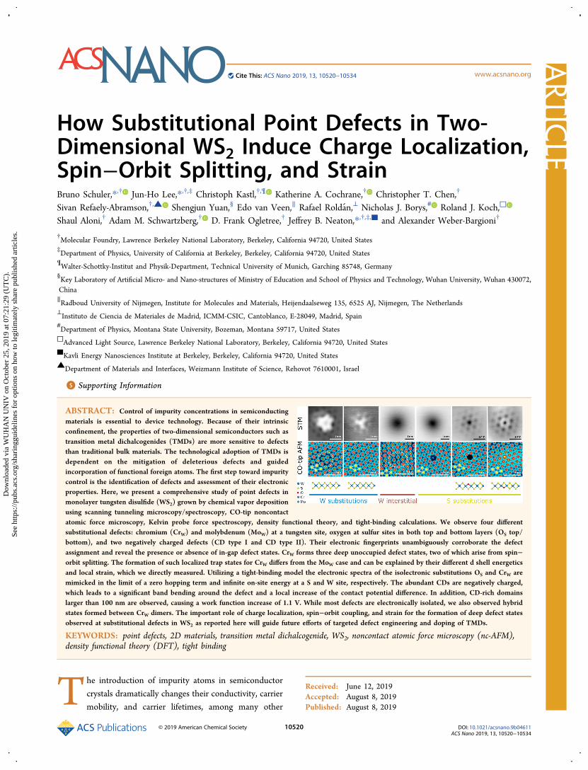
How Substitutional Point Defects in Two- Dimensional WS 2 Induce Charge Localization, Spin−Orbit Splitting, and Strain Bruno Schuler,* ,† Jun-Ho Lee,* ,†,‡ Christoph Kastl, †,¶ Katherine A. Cochrane, † Christopher T. Chen, † Sivan Refaely-Abramson, †,▲ Shengjun Yuan, § Edo van Veen, ∥ Rafael Roldá n, ⊥ Nicholas J. Borys, # Roland J. Koch, □ Shaul Aloni, † Adam M. Schwartzberg, † D. Frank Ogletree, † Jeffrey B. Neaton,* ,†,‡,■ and Alexander Weber-Bargioni † † Molecular Foundry, Lawrence Berkeley National Laboratory, Berkeley, California 94720, United States ‡ Department of Physics, University of California at Berkeley, Berkeley, California 94720, United States ¶ Walter-Schottky-Institut and Physik-Department, Technical University of Munich, Garching 85748, Germany § Key Laboratory of Artificial Micro- and Nano-structures of Ministry of Education and School of Physics and Technology, Wuhan University, Wuhan 430072, China ∥ Radboud University of Nijmegen, Institute for Molecules and Materials, Heijendaalseweg 135, 6525 AJ, Nijmegen, The Netherlands ⊥ Instituto de Ciencia de Materiales de Madrid, ICMM-CSIC, Cantoblanco, E-28049, Madrid, Spain # Department of Physics, Montana State University, Bozeman, Montana 59717, United States □ Advanced Light Source, Lawrence Berkeley National Laboratory, Berkeley, California 94720, United States ■ Kavli Energy Nanosciences Institute at Berkeley, Berkeley, California 94720, United States ▲ Department of Materials and Interfaces, Weizmann Institute of Science, Rehovot 7610001, Israel * S Supporting Information ABSTRACT: Control of impurity concentrations in semiconducting materials is essential to device technology. Because of their intrinsic confinement, the properties of two-dimensional semiconductors such as transition metal dichalcogenides (TMDs) are more sensitive to defects than traditional bulk materials. The technological adoption of TMDs is dependent on the mitigation of deleterious defects and guided incorporation of functional foreign atoms. The first step toward impurity control is the identification of defects and assessment of their electronic properties. Here, we present a comprehensive study of point defects in monolayer tungsten disulfide (WS 2 ) grown by chemical vapor deposition using scanning tunneling microscopy/spectroscopy, CO-tip noncontact atomic force microscopy, Kelvin probe force spectroscopy, density functional theory, and tight-binding calculations. We observe four different substitutional defects: chromium (Cr W ) and molybdenum (Mo W ) at a tungsten site, oxygen at sulfur sites in both top and bottom layers (O S top/ bottom), and two negatively charged defects (CD type I and CD type II). Their electronic fingerprints unambiguously corroborate the defect assignment and reveal the presence or absence of in-gap defect states. Cr W forms three deep unoccupied defect states, two of which arise from spin− orbit splitting. The formation of such localized trap states for Cr W differs from the Mo W case and can be explained by their different d shell energetics and local strain, which we directly measured. Utilizing a tight-binding model the electronic spectra of the isolectronic substitutions O S and Cr W are mimicked in the limit of a zero hopping term and infinite on-site energy at a S and W site, respectively. The abundant CDs are negatively charged, which leads to a significant band bending around the defect and a local increase of the contact potential difference. In addition, CD-rich domains larger than 100 nm are observed, causing a work function increase of 1.1 V. While most defects are electronically isolated, we also observed hybrid states formed between Cr W dimers. The important role of charge localization, spin−orbit coupling, and strain for the formation of deep defect states observed at substitutional defects in WS 2 as reported here will guide future efforts of targeted defect engineering and doping of TMDs. KEYWORDS: point defects, 2D materials, transition metal dichalcogenide, WS 2 , noncontact atomic force microscopy (nc-AFM), density functional theory (DFT), tight binding T he introduction of impurity atoms in semiconductor crystals dramatically changes their conductivity, carrier mobility, and carrier lifetimes, among many other Received: June 12, 2019 Accepted: August 8, 2019 Published: August 8, 2019 Article www.acsnano.org Cite This: ACS Nano 2019, 13, 10520-10534 © 2019 American Chemical Society 10520 DOI: 10.1021/acsnano.9b04611 ACS Nano 2019, 13, 10520−10534 Downloaded via WUHAN UNIV on October 25, 2019 at 07:21:29 (UTC). See https://pubs.acs.org/sharingguidelines for options on how to legitimately share published articles.
Transcript of How Substitutional Point Defects in Two- Article ... · using scanning tunneling...
How Substitutional Point Defects in Two-Dimensional WS2 Induce Charge Localization,Spin−Orbit Splitting, and StrainBruno Schuler,*,† Jun-Ho Lee,*,†,‡ Christoph Kastl,†,¶ Katherine A. Cochrane,† Christopher T. Chen,†
Sivan Refaely-Abramson,†,▲ Shengjun Yuan,§ Edo van Veen,∥ Rafael Roldan,⊥ Nicholas J. Borys,# Roland J. Koch,□
Shaul Aloni,† Adam M. Schwartzberg,† D. Frank Ogletree,† Jeffrey B. Neaton,*,†,‡,■ and Alexander Weber-Bargioni†
†Molecular Foundry, Lawrence Berkeley National Laboratory, Berkeley, California 94720, United States‡Department of Physics, University of California at Berkeley, Berkeley, California 94720, United States¶Walter-Schottky-Institut and Physik-Department, Technical University of Munich, Garching 85748, Germany§Key Laboratory of Artificial Micro- and Nano-structures of Ministry of Education and School of Physics and Technology, Wuhan University, Wuhan 430072,China∥Radboud University of Nijmegen, Institute for Molecules and Materials, Heijendaalseweg 135, 6525 AJ, Nijmegen, The Netherlands⊥Instituto de Ciencia de Materiales de Madrid, ICMM-CSIC, Cantoblanco, E-28049, Madrid, Spain#Department of Physics, Montana State University, Bozeman, Montana 59717, United States□Advanced Light Source, Lawrence Berkeley National Laboratory, Berkeley, California 94720, United States■Kavli Energy Nanosciences Institute at Berkeley, Berkeley, California 94720, United States▲Department of Materials and Interfaces, Weizmann Institute of Science, Rehovot 7610001, Israel
*S Supporting Information
ABSTRACT: Control of impurity concentrations in semiconductingmaterials is essential to device technology. Because of their intrinsicconfinement, the properties of two-dimensional semiconductors such astransition metal dichalcogenides (TMDs) are more sensitive to defectsthan traditional bulk materials. The technological adoption of TMDs isdependent on the mitigation of deleterious defects and guidedincorporation of functional foreign atoms. The first step toward impuritycontrol is the identification of defects and assessment of their electronicproperties. Here, we present a comprehensive study of point defects inmonolayer tungsten disulfide (WS2) grown by chemical vapor depositionusing scanning tunneling microscopy/spectroscopy, CO-tip noncontactatomic force microscopy, Kelvin probe force spectroscopy, density functional theory, and tight-binding calculations. We observe four differentsubstitutional defects: chromium (CrW) and molybdenum (MoW) at a tungsten site, oxygen at sulfur sites in both top and bottom layers (OS top/bottom), and two negatively charged defects (CD type I and CD type II). Their electronic fingerprints unambiguously corroborate the defectassignment and reveal the presence or absence of in-gap defect states. CrW forms three deep unoccupied defect states, two of which arise from spin−orbit splitting. The formation of such localized trap states for CrW differs from the MoW case and can be explained by their different d shell energeticsand local strain, which we directly measured. Utilizing a tight-binding model the electronic spectra of the isolectronic substitutions OS and CrW aremimicked in the limit of a zero hopping term and infinite on-site energy at a S and W site, respectively. The abundant CDs are negatively charged,which leads to a significant band bending around the defect and a local increase of the contact potential difference. In addition, CD-rich domainslarger than 100 nm are observed, causing a work function increase of 1.1 V. While most defects are electronically isolated, we also observed hybridstates formed between CrW dimers. The important role of charge localization, spin−orbit coupling, and strain for the formation of deep defect statesobserved at substitutional defects in WS2 as reported here will guide future efforts of targeted defect engineering and doping of TMDs.
KEYWORDS: point defects, 2D materials, transition metal dichalcogenide, WS2, noncontact atomic force microscopy (nc-AFM),density functional theory (DFT), tight binding
The introduction of impurity atoms in semiconductor
crystals dramatically changes their conductivity, carrier
mobility, and carrier lifetimes, among many other
Received: June 12, 2019Accepted: August 8, 2019Published: August 8, 2019
Artic
lewww.acsnano.orgCite This: ACS Nano 2019, 13, 10520−10534
© 2019 American Chemical Society 10520 DOI: 10.1021/acsnano.9b04611ACS Nano 2019, 13, 10520−10534
Dow
nloa
ded
via
WU
HA
N U
NIV
on
Oct
ober
25,
201
9 at
07:
21:2
9 (U
TC
).Se
e ht
tps:
//pub
s.ac
s.or
g/sh
arin
ggui
delin
es f
or o
ptio
ns o
n ho
w to
legi
timat
ely
shar
e pu
blis
hed
artic
les.
properties down to impurity concentrations at the parts perbillion level. This extreme sensitivity to impurities requireddeveloping effective purification methods and strategies tomitigate the impact of defects, for instance by passivation, and toestablish precisely controlled introduction of dopants, thefoundation of modern semiconductor technology. Today,similar challenges are faced in two-dimensional (2D) materialsscience. Because of their intrinsic electron confinement, 2Dmaterials are even more susceptible to structural defects.1
Anticipating which defects or impurities are introduced duringsynthesis is often impossible given the complexity of reactionpathways and environmental variables. Moreover, predictingdefect functionality, particularly for highly correlated materials,is far from trivial even with today’s advanced theoreticalmethods and computational power. Identifying defects exper-imentally and probing their electronic structure is equallychallenging, as it requires correlating the defect’s atomic andelectronic structure with atomic precision and milli-electronvoltenergy resolution.Monolayer transition metal dichalcogenides (TMDs)2,3 are a
remarkable class of 2D materials in several ways. Many aresemiconducting (depending on composition and structure) witha direct band gap in the visible or near-infrared range, makingthem attractive for optoelectronic applications.4 They aresynthesizable by several established methods [chemical vapordeposition (CVD), metal organic chemical vapor deposition(MOCVD), atomic layer deposition (ALD), and molecularbeam epitaxy (MBE)].5 They exhibit strong light−matterinteractions,6 unique photophysics,7,8 strong spin−orbit cou-pling,9 and prominent many-body effects due to enhancedCoulomb interactions,10,11 exemplified by the hundredfoldenhancement of exciton binding energies as compared to bulksemiconductors.12
Tuning electronic, optical, and catalytic properties of 2Dmaterials by means of defect engineering, in particular chemicaldoping, is a highly anticipated technology in the field.1 In bulksemiconductors, shallow donor or acceptor states are typicallyused to control the carrier concentration. In 2D semiconductors,quantum confinement and screening effects generally lead todeeper defect energy levels and increasing defect ionizationenergies.13 On the one hand, this limits the attainable free chargecarrier concentration by chemical doping.13 On the other hand,surface-bound deep defect levels are an ideal system fordesigning single-photon emitters14,15 and catalysts.1
Structural defects such as domain boundaries,16−18 disloca-tions,18,19 vacancies,16,18,20−22 interstitial atoms,18 antisitedefects,16,18 and impurities18,20,21,23−25 have been previouslyidentified in TMDs and studied theoretically.26−34 Such defectsare believed to modify charge transport,35 to host defect-boundexcitons,36−39 and to act as single-photon quantum emit-ters.15,40−43 It is also suspected that point defects representactive sites in catalytic processes on the otherwise inert TMDsurface.44−46 In light of these anticipated functionalities thereare growing efforts toward targeted incorporation of substitu-tional defects for doping and alloying of TMDs to tune theirelectronic, magnetic, optical, and catalytic properties.18,47−50
Establishing structure−function relationships for such defectsor dopants is, however, challenging. Oftenmacro- or mesoscopicensemble measurements are correlated with atomic-resolutionmicroscopy techniques to infer a certain defect functionality.The presence or prevalence of a certain defect does notnecessarily indicate causality of the observed property. Instead,electronic and optical properties need to be measured locally to
establish an unambiguous link to a specific structural defect.Moreover, twomajor complications impede defect identificationitself by using the two prime experimental methods, aberration-corrected transmission electron microscopy (AC-TEM) andscanning tunneling microscopy (STM). First, TMDs areelectron beam sensitive, which can cause in situ generation ofde f ec t s i n pa r t i cu l a r cha l cogen vacanc i e sbyTEM.16,18,20,30,35,51 Second, identification of defect atomicstructure by STM is very challenging because the STM contrastis dominated by electronic effects, which has led to contradictorydefect assignments by STM-only studies.52−54 Both of thesecomplications have supported the notion that chalcogenvacancy defects are abundant in as-grown TMDs under ambientconditions, which we have recently challenged.22,25 We showedthat oxygen substituting sulfur is the most abundant point defectin CVD-grown WS2,
25 and chalcogen vacancies, which areabsent in as-grown samples, can be created by high-temperatureannealing under vacuum.22
Here, we report the direct correlation of the atomic andelectronic structure of commonly observed point defects inCVD-grown monolayer WS2 samples using a combination oflow-temperature scanning tunneling microscopy/spectroscopy(STM/STS), CO-tip noncontact atomic force microscopy (nc-AFM), Kelvin probe force spectroscopy (KPFS), densityfunctional theory (DFT), and tight-binding calculations. Sixpoint defects occurring in as-grown samples were found andinvestigated. Four of them were identified as W or Ssubstitutions: CrW (chromium substituting tungsten), MoW(molybdenum substituting tungsten), and OS (oxygen sub-stituting sulfur) in the top and bottom sulfur layer. In addition,we observed two types of negatively charged defects (CDs),where the impurity atom could not be unambiguously identified.We discuss in detail the electronic defect states associated
with each of these defects. Particularly the roles of spin−orbitcoupling, crystal-field splitting, and strain are analyzed, and theorigin of the qualitatively different behavior of isoelectronicsubstituents is examined. One case of defect state hybridizationis discussed. Furthermore, the negative charge localization attwo types of defects is demonstrated, which induces significantlocal band bending and a dramatically higher work function ofmesoscopic CD-rich domains.These results advance our understanding of the role of defects
in TMDs. Unambiguous chemical assignment of defectssuggests formation pathways, optimized synthetic processes,and routes to controlled chemical doping. Detailed structuraland electronic characterization provides insights into underlyingfundamental physical principles. Of particular interest is theobservation of spin−orbit split deep in-gap states for CrW andthe annealing-induced sulfur vacancy as well as the defect-boundcharge at both CDs. The latter can be expected to form boundtrions, scatter charge carriers, and act as an efficientrecombination site, while the former are potential candidatesfor single-photon emitters.
RESULTS AND DISCUSSIONMonolayer WS2 was grown using a CVD process on epitaxialgraphene (Gr) on SiC(0001).55−57 The tungsten oxide (WO2.9)powder and H2S gas precursor streams were compartmentalizedto prevent sulfurization of the transition metal oxide precursorduring growth.57,58 More details on the sample growth andpreparation prior to low-temperature scanning probe inspectioncan be found in the Methods section and ref 57. The Gr/SiCsubstrate only weakly interacts with the WS2 layer, preserving its
ACS Nano Article
DOI: 10.1021/acsnano.9b04611ACS Nano 2019, 13, 10520−10534
10521
interesting intrinsic band structure, such as the direct band gapin the visible range and the spin−orbit splitting at the K-point.56,57 The most notable exception is a substrate-inducedpinning of the WS2 Fermi level to the upper third of the bandgap, near the conduction band edge.56,59 The reported values ofthe substrate-induced doping vary between different studies,most likely as a consequence of varying growth conditions,which can affect the interfacial states of the graphene/bufferlayer system, for instance through intercalation.60 Also, thequasiparticle band gap becomes smaller with increasing numberof graphene layers due to the increased substrate screening (seeSupporting Information).10
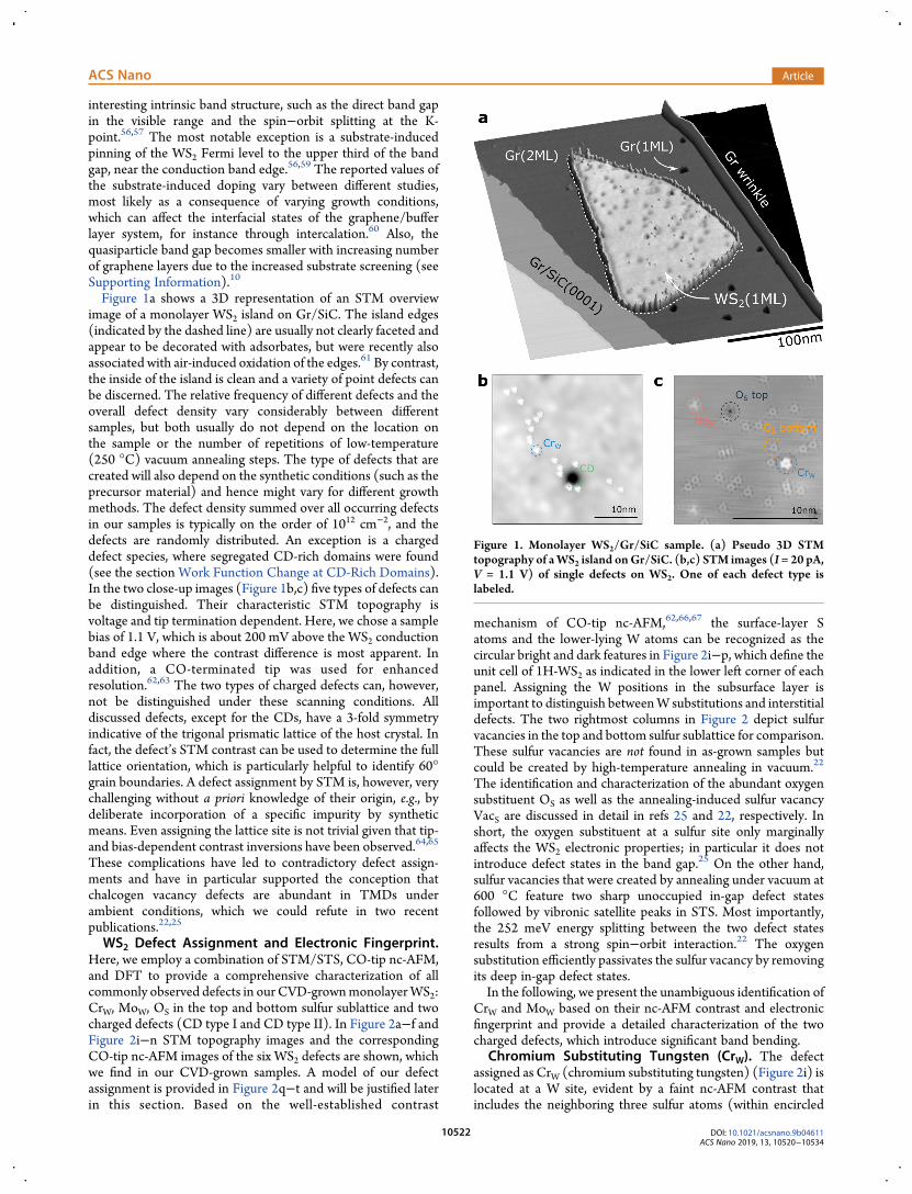
Figure 1a shows a 3D representation of an STM overviewimage of a monolayer WS2 island on Gr/SiC. The island edges(indicated by the dashed line) are usually not clearly faceted andappear to be decorated with adsorbates, but were recently alsoassociated with air-induced oxidation of the edges.61 By contrast,the inside of the island is clean and a variety of point defects canbe discerned. The relative frequency of different defects and theoverall defect density vary considerably between differentsamples, but both usually do not depend on the location onthe sample or the number of repetitions of low-temperature(250 °C) vacuum annealing steps. The type of defects that arecreated will also depend on the synthetic conditions (such as theprecursor material) and hence might vary for different growthmethods. The defect density summed over all occurring defectsin our samples is typically on the order of 1012 cm−2, and thedefects are randomly distributed. An exception is a chargeddefect species, where segregated CD-rich domains were found(see the section Work Function Change at CD-Rich Domains).In the two close-up images (Figure 1b,c) five types of defects canbe distinguished. Their characteristic STM topography isvoltage and tip termination dependent. Here, we chose a samplebias of 1.1 V, which is about 200 mV above the WS2 conductionband edge where the contrast difference is most apparent. Inaddition, a CO-terminated tip was used for enhancedresolution.62,63 The two types of charged defects can, however,not be distinguished under these scanning conditions. Alldiscussed defects, except for the CDs, have a 3-fold symmetryindicative of the trigonal prismatic lattice of the host crystal. Infact, the defect’s STM contrast can be used to determine the fulllattice orientation, which is particularly helpful to identify 60°grain boundaries. A defect assignment by STM is, however, verychallenging without a priori knowledge of their origin, e.g., bydeliberate incorporation of a specific impurity by syntheticmeans. Even assigning the lattice site is not trivial given that tip-and bias-dependent contrast inversions have been observed.64,65
These complications have led to contradictory defect assign-ments and have in particular supported the conception thatchalcogen vacancy defects are abundant in TMDs underambient conditions, which we could refute in two recentpublications.22,25
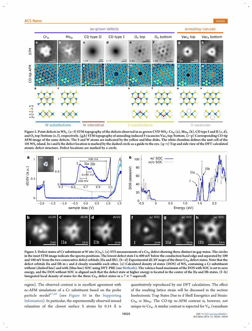
WS2 Defect Assignment and Electronic Fingerprint.Here, we employ a combination of STM/STS, CO-tip nc-AFM,and DFT to provide a comprehensive characterization of allcommonly observed defects in our CVD-grownmonolayerWS2:CrW, MoW, OS in the top and bottom sulfur sublattice and twocharged defects (CD type I and CD type II). In Figure 2a−f andFigure 2i−n STM topography images and the correspondingCO-tip nc-AFM images of the six WS2 defects are shown, whichwe find in our CVD-grown samples. A model of our defectassignment is provided in Figure 2q−t and will be justified laterin this section. Based on the well-established contrast
mechanism of CO-tip nc-AFM,62,66,67 the surface-layer Satoms and the lower-lying W atoms can be recognized as thecircular bright and dark features in Figure 2i−p, which define theunit cell of 1H-WS2 as indicated in the lower left corner of eachpanel. Assigning the W positions in the subsurface layer isimportant to distinguish betweenW substitutions and interstitialdefects. The two rightmost columns in Figure 2 depict sulfurvacancies in the top and bottom sulfur sublattice for comparison.These sulfur vacancies are not found in as-grown samples butcould be created by high-temperature annealing in vacuum.22
The identification and characterization of the abundant oxygensubstituent OS as well as the annealing-induced sulfur vacancyVacS are discussed in detail in refs 25 and 22, respectively. Inshort, the oxygen substituent at a sulfur site only marginallyaffects the WS2 electronic properties; in particular it does notintroduce defect states in the band gap.25 On the other hand,sulfur vacancies that were created by annealing under vacuum at600 °C feature two sharp unoccupied in-gap defect statesfollowed by vibronic satellite peaks in STS. Most importantly,the 252 meV energy splitting between the two defect statesresults from a strong spin−orbit interaction.22 The oxygensubstitution efficiently passivates the sulfur vacancy by removingits deep in-gap defect states.In the following, we present the unambiguous identification of
CrW and MoW based on their nc-AFM contrast and electronicfingerprint and provide a detailed characterization of the twocharged defects, which introduce significant band bending.
Chromium Substituting Tungsten (CrW). The defectassigned as CrW (chromium substituting tungsten) (Figure 2i) islocated at a W site, evident by a faint nc-AFM contrast thatincludes the neighboring three sulfur atoms (within encircled
Figure 1. Monolayer WS2/Gr/SiC sample. (a) Pseudo 3D STMtopography of aWS2 island onGr/SiC. (b,c) STM images (I = 20 pA,V = 1.1 V) of single defects on WS2. One of each defect type islabeled.
ACS Nano Article
DOI: 10.1021/acsnano.9b04611ACS Nano 2019, 13, 10520−10534
10522
region). The observed contrast is in excellent agreement withnc-AFM simulations of a Cr substituent based on the probeparticle model67,68 (see Figure S6 in the SupportingInformation). In particular, the experimentally observed inwardrelaxation of the closest surface S atoms by 0.14 Å is
quantitatively reproduced by our DFT calculations. The effectof the resulting lattice strain will be discussed in the sectionIsoelectronic Trap States Due to d Shell Energetics and Strain:CrW vs MoW. The CO-tip nc-AFM contrast is, however, notunique to CrW. A similar contrast is expected for VW (vanadium
Figure 2. Point defects inWS2. (a−f) STM topography of the defects observed in as-grownCVD-WS2: CrW (a), MoW (b), CD type I and II (c, d),andOS top/bottom (e, f), respectively. (g,h) STM topography of annealing-induced S vacancies VacS top/bottom. (i−p) Corresponding CO-tipAFM image of the same defects. The S and W atoms are indicated by the yellow and blue disks. The white rhombus defines the unit cell of the1H-WS2 island. In i and k the defect location is marked by the dashed circle as a guide to the eye. (q−v) Top and side view of the DFT-calculatedatomic defect structure. Defect locations are marked by a circle.
Figure 3. Defect states of Cr substituent at W site (CrW). (a) STSmeasurements of a CrW defect showing three distinct in-gap states. The circlesin the inset STM image indicate the spectra positions. The lowest defect state I is 400mV below the conduction band edge and separated by 100and 180mV from the two consecutive defect orbitals (IIa and IIb). (b−d) Experimental dI/dVmaps of the three CrW defect states. Note that thedefect orbitals IIa and IIb in c and d closely resemble each other. (e) Calculated density of states (DOS) of WS2 containing a Cr substituentwithout (dashed line) and with (blue line) SOC using DFT-PBE (seeMethods). The valence bandmaximum of the DOSwith SOC is set to zeroenergy, and the DOS without SOC is aligned such that the defect state at higher energy is located in the center of the IIa and IIb states. (f−h)Integrated local density of states for the three CrW defect states in a 7 × 7 supercell.
ACS Nano Article
DOI: 10.1021/acsnano.9b04611ACS Nano 2019, 13, 10520−10534
10523
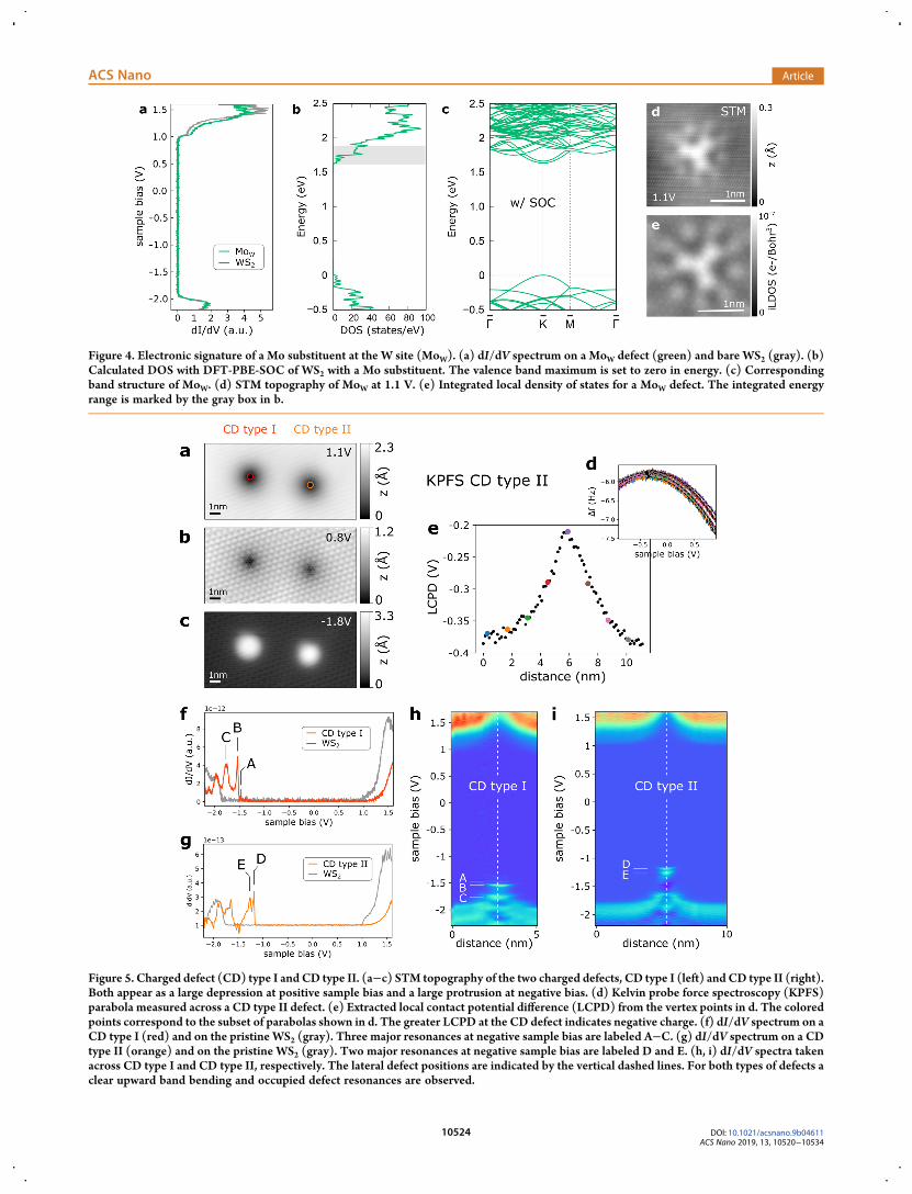
Figure 4. Electronic signature of a Mo substituent at the W site (MoW). (a) dI/dV spectrum on a MoW defect (green) and bare WS2 (gray). (b)Calculated DOS with DFT-PBE-SOC of WS2 with a Mo substituent. The valence band maximum is set to zero in energy. (c) Correspondingband structure of MoW. (d) STM topography of MoW at 1.1 V. (e) Integrated local density of states for a MoW defect. The integrated energyrange is marked by the gray box in b.
Figure 5. Charged defect (CD) type I and CD type II. (a−c) STM topography of the two charged defects, CD type I (left) and CD type II (right).Both appear as a large depression at positive sample bias and a large protrusion at negative bias. (d) Kelvin probe force spectroscopy (KPFS)parabola measured across a CD type II defect. (e) Extracted local contact potential difference (LCPD) from the vertex points in d. The coloredpoints correspond to the subset of parabolas shown in d. The greater LCPD at the CD defect indicates negative charge. (f) dI/dV spectrum on aCD type I (red) and on the pristine WS2 (gray). Three major resonances at negative sample bias are labeled A−C. (g) dI/dV spectrum on a CDtype II (orange) and on the pristine WS2 (gray). Two major resonances at negative sample bias are labeled D and E. (h, i) dI/dV spectra takenacross CD type I and CD type II, respectively. The lateral defect positions are indicated by the vertical dashed lines. For both types of defects aclear upward band bending and occupied defect resonances are observed.
ACS Nano Article
DOI: 10.1021/acsnano.9b04611ACS Nano 2019, 13, 10520−10534
10524
substituting tungsten), MnW (manganese substituting tung-sten), OW, and SW (see Figure S7). However, the defect’selectronic signature unambiguously identifies it as CrW asdiscussed below.The chromium substituent can be readily observed in the
STM topography as a 3-fold symmetric protrusion whentunneling into unoccupied states at positive sample bias (seeFigure 1b,c and Figure 2a). In Figure 3a, a differentialconductance (dI/dV) spectrum of a CrW is shown, revealingthree distinct defect resonances at 400 mV (denoted I), 300 mV(denoted IIa), and 220 mV (denoted IIb) below the conductionband minimum. These resonances are indicative of localizedunoccupied defect states. dI/dV images at these resonanceenergies displayed in Figure 3b−d map out the correspondingdefect states with a spatial extent of about 1 nm. Intriguingly, thetwo defect states at higher energies (denoted IIa and IIb) appearvery similar, indicating a lifted orbital degeneracy.The calculated DFT density of states for a Cr substituent
(Figure 3e) and the shape of its associated defect orbitals(Figure 3f−h) closely resemble the experimental findings (seeMethods for details of our calculations). The close correspond-ence of experiment and theory corroborates our defectassignment as CrW. Other possible candidates such as V orMn substituents can be ruled out, as the former does not exhibitany in-gap state, and the defect states of the latter aredistinctively different from experiment (see Figure S13).By comparing DFT calculations with and without spin−orbit
coupling (solid blue and dashed gray line in Figure 3e,
respectively) we find that the Δ ≈ 48 meV splitting betweenIIa and IIb is a consequence of the spin−orbit interaction. Thiseffect will be further discussed in the section Spin-Orbit Splittingof CrW Detect States.Cr substituents in CVD-grown MoS2 on SiO2 have recently
also been detected by single-atom electron energy lossspectroscopy,69 suggesting that this substitutional transitionmetal atom is stable under electron irradiation and common inTMD samples.
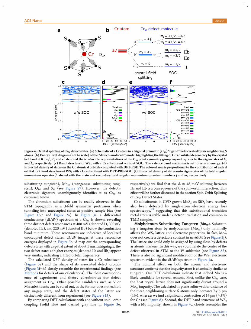
Molybdenum Substituting Tungsten (MoW). Substitut-ing a tungsten atom by molybdenum (MoW) only minimallyaffects the WS2 lattice and electronic properties. In fact, MoWdoes not create a detectable contrast in nc-AFM (see Figure 2j).The lattice site could only be assigned by using close-by defectsas atomic markers. In this way, we could relate the center of thedefect observed in STM to the W sublattice (see Figure S3).There is also no significant modification of the WS2 electronicspectrum evident in the dI/dV spectrum in Figure 4a.The minimal effect on both the atomic and electronic
structure confirms that the impurity atom is chemically similar totungsten. Our DFT calculations indicate that indeed Mo is alikely candidate for several reasons. First, unlike the CrW case,the host crystal lattice does not significantly distort around aMoW impurity. The calculated in-plane sulfur−sulfur distance ofthe three neighboring surface S atoms only increases by 3 pm(1%), whereas we find a significant contraction of 14 pm (4.5%)for Cr (see Figure 8). Second, the DFT band structure of WS2with a Mo impurity, shown in Figure 4c, closely resembles the
Figure 6. Orbital splitting of CrW defect states. (a) Schematic of a Cr atom in a trigonal prismatic (D3h) “ligand” field created by six neighboring Satoms. (b) Energy level diagram (not to scale) of the “defect−molecule”model highlighting the lifting of Cr’s d orbital degeneracy by the crystalfield and SOC. a1′, e′, and e″ denoted the irreducible representations of the D3h point symmetry group. ml and mj refer to the eigenstates of Lzand Jz, respectively. (c) Band structure of WS2 with a Cr substituent without SOC. The valence band maximum is set to zero in energy. (d)Projected density of states on the Cr atomic d orbitals computed with DFT-PBE. The colored area is proportional to the contribution of each dorbital. (e) Band structure ofWS2 with a Cr substituent with DFT-PBE-SOC. (f) Projected density of states onto eigenstates of the total angularmomentum operator J labeled with the main and secondary total angular momentum quantum numbers j and mj, respectively.
ACS Nano Article
DOI: 10.1021/acsnano.9b04611ACS Nano 2019, 13, 10520−10534
10525

band structure of pristine monolayer WS2. Nonetheless, slight
modulations of the local density of states lead to a characteristic
shape observed in STM (Figure 4d) that is nicely reproduced by
the DFT integrated local density of state (ILDOS) of MoW(Figure 4e), confirming our assignment.
We postulate that the source of the Cr and Mo is the WO2.9
CVD precursor (99.99%, Alfa Aesar), which contains 1 ppm ofCr and 8 ppm Mo impurities (according to the certificate ofanalysis). A 1 ppm impurity concentration translates into adoping density of 2.3× 109 cm−2. Our observed impurity densityof CrW and MoW is on the order of 1010 cm−2, which is plausible
Figure 7. Hybrid states of a CrW dimer. (a) STM topography of a CrW dimer in the third-nearest-neighbor configuration. (b) CO-tip nc-AFMimage of the same dimer. (c) Extracted S−S distance of the nc-AFM image shown in b revealing the local lattice strain. (d, e) dI/dV spectrarecorded across the dimer (direction indicated by arrow in a). Six hybrid dimer states are marked by the dashed lines and arrows in e. The threesingle CrW states (I, IIa, IIb) are indicated for comparison. (f) DFTmodel of the sameCrW dimer. (g, h) DFT band structure of the CrW dimer ina 7 × 7 supercell without (g) and with SOC (h). The six hybrid CrW dimer states are marked with blue arrows, and the three lines (I, IIa, IIb)indicate the calculated defect states of a single CrW for comparison.
Figure 8. CrW vs MoW: strain and d orbital hybridization. (a, b) DFT-calculated relaxed defect geometry for CrW and MoW. The dashed linesindicate the sulfur−sulfur (S−S) distance in direct proximity of the substitute. This distance is considerably smaller (3.01 Å) for CrW ascompared to perfect WS2 (3.15 Å), indicating compressive strain. (c, d) Simulated CO-tip nc-AFM images based on the probe particlemodel67,68 using the defect geometries shown in a and b. (e, f) Experimental CO-tip nc-AFM image of CrW andMoW. In c−f the atom positionshave been determined using the Atomap88 fitting routine, revealing the local strain around CrW and its absence around MoW in both thesimulation and experiment. The % strain scale has been corrected for the CO tip tilting. (g, h) DFT-projected DOS onto Cr and Mo d orbitalsshowing the degree of hybridization.
ACS Nano Article
DOI: 10.1021/acsnano.9b04611ACS Nano 2019, 13, 10520−10534
10526
given that the evaporation and incorporation process of thesespecies during CVD could be different from majority tungsten.In contrast to this dilute doping regime, other groups havedeliberately synthesized ternary TMD alloys such asMox−1WxS2
47 or Mox−1WxSe248,49 to continuously tune the
band gap of TMDs.Consistent with our experimental results, we find that Cr and
Mo impurities at a tungsten site exhibit a much lower formationenergy as compared to a sulfur or interstitial site. For CrW, aformation energy of 0.31 eV (W-rich limit) and 0.03 eV (S-richlimit) was calculated, whereas CrS yields 4.72 eV (W-rich limit)and 4.86 eV (S-rich limit) and Cri yields 6.70 eV. These valuesare obtained considering WO2.9 and H2S as the source of W andS, respectively. In the Supporting Information, more details onthe calculation method of formation energies can be found. ForMoW, MoS, and Moi we find a similar trend. This explains whyonly CrW andMoW are thermodynamically stable and frequentlyobserved in our samples. We note that recent DFT calculationsreveal that many transition metals at an interstitial site areenergetically favorable in MoTe2 where the in-plane latticeconstant is ∼11% larger as compared to WS2.
70 In WS2, therelatively small interatomic spacing renders interstitial atomsunfavorable. We also find that O impurities at sulfur sites have asignificantly lower formation energy [0.54 eV (0.58 eV) for W-rich (S-rich) conditions] than a sulfur vacancy [1.53 eV (1.67eV) for W-rich (S-rich) conditions], in line with ourobservations reported in refs 22 and 25.Charged Defects Type I and Type II. The most easily
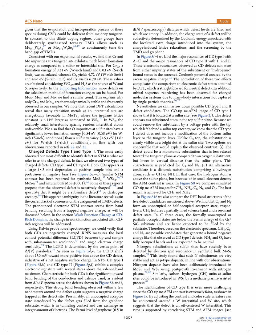
observed but most difficult to identify defect in STM is what werefer to as the charged defect. In fact, we observed two types ofcharged defects, CD type I and CD type II. Both CDs appears asa large (∼3 nm) depression at positive sample bias and aprotrusion at negative bias (see Figure 5a−c). Similar STMcontrast has been reported for synthetic MoS2,
52 WSe2,54,71
MoSe271 and natural bulk MoS2(0001).
72 Some of these reportspropose that the observed defect is negatively charged71,72 andspeculate that it might be a subsurface defect52 or chalcogenvacancy.54 This apparent ambiguity in the literature reveals againthe current lack of consensus on the assignment of TMDdefects.The pronounced electronic STM contrast stems from bandbending resulting from a trapped negative charge, as will bediscussed below. In the section Work Function Change at CD-Rich Domains, the change in work function associated with CD-rich regions will be addressed.Using Kelvin probe force spectroscopy, we could verify that
both CDs are negatively charged. KPFS measures the localcontact potential difference (LCPD) between tip and samplewith sub-nanometer resolution73 and single electron chargesensitivity.74 The LCPD is determined by the vertex point ofΔf(V) parabolas.74 As seen in Figure 5d,e, the LCPD shiftsabout 150 mV toward more positive bias above the CD defect,indicative of a net negative surface charge. In STS, CD type I(Figure 5f,h) and CD type II (Figure 5g,i) exhibit a complexelectronic signature with several states above the valence bandmaximum. Characteristic for both CDs is the significant upwardband bending of the conduction and valence band, as evidentfrom dI/dV spectra across the defects shown in Figure 5h and i,respectively. This strong band bending observed within a fewnanometers around the defect again suggests a negative chargetrapped at the defect site. Presumably, an unoccupied acceptorstate introduced by the defect gets filled from the graphenesubstrate, which is in tunneling contact and can exchange aninteger amount of electrons. The Fermi level of graphene (0 V in
dI/dV spectroscopy) dictates which defect levels are filled andwhich are empty. In addition, the charge state of a defect will becollectively determined by the Coulomb energy associated withthe localized extra charge introduced into the system, thecharge-induced lattice relaxations, and the screening by theTMD and graphene.In Figure 5f−i we label themajor resonances of CD type I with
A−C and the major resonances of CD type II with D and E.These electronic resonances observed at CD defects can stemfrom either impurity states of the substituent or “hydrogenic”bound states in the screened Coulomb potential created by theexcess negative charge.75 The convolution of these two effectscomplicates the comparison to electronic defect states obtainedby DFT, which is straightforward for neutral defects. In addition,orbital sequence reordering has been observed for chargedmolecular systems due to many-body interactions not capturedby single-particle theories.76,77
Nevertheless we can narrow down possible CD type I and IIdefect candidates. The CO-tip nc-AFM image of CD type Ishows that it is located at a sulfur site (see Figure 2l). The defectappears as a substituted atom in the top sulfur plane. Because wecould remove the substituent by a voltage pulse with the tip,which left behind a sulfur top vacancy, we know that the CD typeI defect does not include a modification of the bottom sulfurlayer or the tungsten layer. Unlike OS top, the substitution isclearly visible as a bright dot at the sulfur site. Two options areconceivable that would explain the observed contrast: (i) Thedefect could be a monatomic substitution that is less relaxedtoward the tungsten plane as compared to an oxygen substituent,but lower in vertical distance than the sulfur plane. Thischaracteristic is predicted for CS and NS. (ii) An alternativecandidate is a diatomic substitution comprising a hydrogenatom, such as CH or NH. In that case, the hydrogen atom isabove the sulfur plane, but because of its small electron densitythe AFM contrast is weak. In Figure S8 we compare simulatedCO-tip nc-AFM images for CHS, NHS, CS, NS, and OS. The bestmatch is achieved for CHS and NHS.In Figure S16 we also compare the DFT band structures of the
five defect candidates mentioned above. We find that CS and NSform an unoccupied or half-occupied acceptor state, respec-tively. CHS features a partially filled valence band and a resonantdefect state. In all three cases, the formally unoccupied orpartially occupied states are below the Fermi energy of the Gr/SiC substrate and are hence expected to be filled by thesubstrate. Therefore, based on the electronic spectrum, CHS, CS,and NS are possible candidates that generate a bound negativecharge like that observed at CD type I defects. NHS and OS havefully occupied bands and are expected to be neutral.Nitrogen substitutions at sulfur sites have recently been
detected by electron spin resonance in synthetic bulk MoS2samples.78 This study found that such N substituents are verystable and act as p-type dopants, in line with our observations.Nitrogen dopants have also been deliberately introduced inMoS2 and WS2 using postgrowth treatment with nitrogenplasma.79,80 Similarly, carbon−hydrogen (CH) units at sulfursites could be introduced in WS2 by a methane plasma-assistedprocess.81
The identification of CD type II is even more challengingsince the CO-tip nc-AFM contrast is extremely faint, as shown inFigure 2k. By adjusting the contrast and color scale, a feature canbe conjectured around a W interstitial and W site, whichsuggests that the defect is an off-centered W interstitial. Thisview is supported by correlating STM and AFM images (see
ACS Nano Article
DOI: 10.1021/acsnano.9b04611ACS Nano 2019, 13, 10520−10534
10527
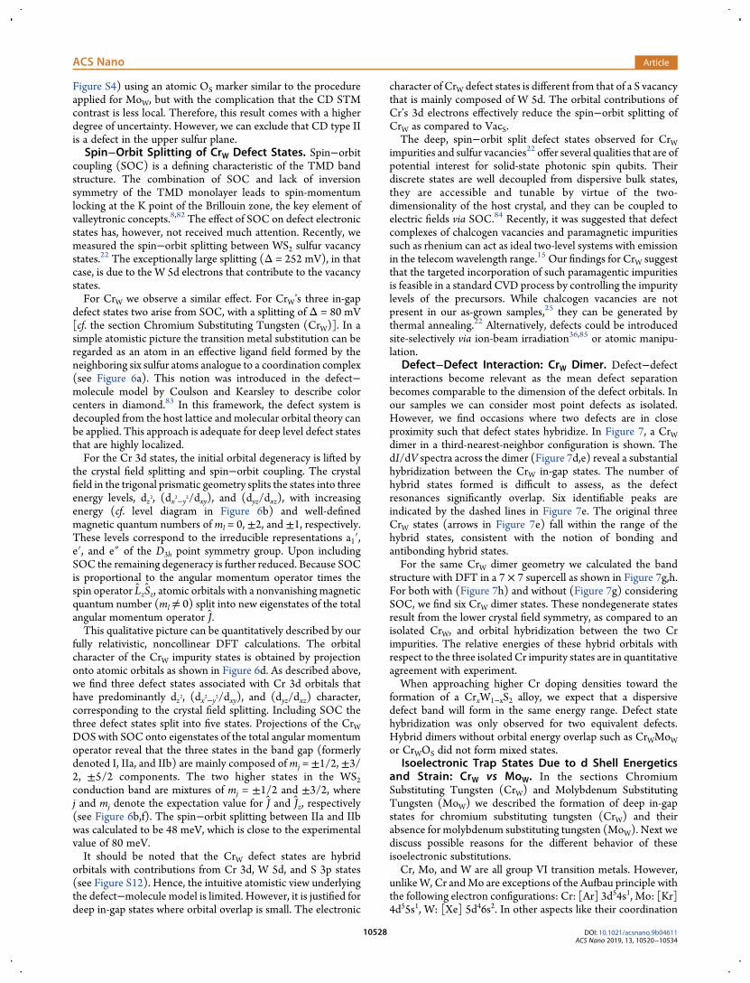
Figure S4) using an atomic OS marker similar to the procedureapplied for MoW, but with the complication that the CD STMcontrast is less local. Therefore, this result comes with a higherdegree of uncertainty. However, we can exclude that CD type IIis a defect in the upper sulfur plane.Spin−Orbit Splitting of CrW Defect States. Spin−orbit
coupling (SOC) is a defining characteristic of the TMD bandstructure. The combination of SOC and lack of inversionsymmetry of the TMD monolayer leads to spin-momentumlocking at the K point of the Brillouin zone, the key element ofvalleytronic concepts.8,82 The effect of SOC on defect electronicstates has, however, not received much attention. Recently, wemeasured the spin−orbit splitting between WS2 sulfur vacancystates.22 The exceptionally large splitting (Δ = 252 mV), in thatcase, is due to the W 5d electrons that contribute to the vacancystates.For CrW we observe a similar effect. For CrW’s three in-gap
defect states two arise from SOC, with a splitting of Δ = 80 mV[cf. the section Chromium Substituting Tungsten (CrW)]. In asimple atomistic picture the transition metal substitution can beregarded as an atom in an effective ligand field formed by theneighboring six sulfur atoms analogue to a coordination complex(see Figure 6a). This notion was introduced in the defect−molecule model by Coulson and Kearsley to describe colorcenters in diamond.83 In this framework, the defect system isdecoupled from the host lattice and molecular orbital theory canbe applied. This approach is adequate for deep level defect statesthat are highly localized.For the Cr 3d states, the initial orbital degeneracy is lifted by
the crystal field splitting and spin−orbit coupling. The crystalfield in the trigonal prismatic geometry splits the states into threeenergy levels, dz2, (dx2−y2/dxy), and (dyz/dxz), with increasingenergy (cf. level diagram in Figure 6b) and well-definedmagnetic quantum numbers of ml = 0, ±2, and ±1, respectively.These levels correspond to the irreducible representations a1′,e′, and e″ of the D3h point symmetry group. Upon includingSOC the remaining degeneracy is further reduced. Because SOCis proportional to the angular momentum operator times thespin operator LzSz, atomic orbitals with a nonvanishingmagneticquantum number (ml ≠ 0) split into new eigenstates of the totalangular momentum operator J.This qualitative picture can be quantitatively described by our
fully relativistic, noncollinear DFT calculations. The orbitalcharacter of the CrW impurity states is obtained by projectiononto atomic orbitals as shown in Figure 6d. As described above,we find three defect states associated with Cr 3d orbitals thathave predominantly dz2, (dx2−y2/dxy), and (dyz/dxz) character,corresponding to the crystal field splitting. Including SOC thethree defect states split into five states. Projections of the CrWDOSwith SOC onto eigenstates of the total angular momentumoperator reveal that the three states in the band gap (formerlydenoted I, IIa, and IIb) are mainly composed ofmj = ±1/2, ±3/2, ±5/2 components. The two higher states in the WS2conduction band are mixtures of mj = ±1/2 and ±3/2, wherej and mj denote the expectation value for J and Jz, respectively(see Figure 6b,f). The spin−orbit splitting between IIa and IIbwas calculated to be 48 meV, which is close to the experimentalvalue of 80 meV.It should be noted that the CrW defect states are hybrid
orbitals with contributions from Cr 3d, W 5d, and S 3p states(see Figure S12). Hence, the intuitive atomistic view underlyingthe defect−molecule model is limited. However, it is justified fordeep in-gap states where orbital overlap is small. The electronic
character of CrW defect states is different from that of a S vacancythat is mainly composed of W 5d. The orbital contributions ofCr’s 3d electrons effectively reduce the spin−orbit splitting ofCrW as compared to VacS.The deep, spin−orbit split defect states observed for CrW
impurities and sulfur vacancies22 offer several qualities that are ofpotential interest for solid-state photonic spin qubits. Theirdiscrete states are well decoupled from dispersive bulk states,they are accessible and tunable by virtue of the two-dimensionality of the host crystal, and they can be coupled toelectric fields via SOC.84 Recently, it was suggested that defectcomplexes of chalcogen vacancies and paramagnetic impuritiessuch as rhenium can act as ideal two-level systems with emissionin the telecom wavelength range.15 Our findings for CrW suggestthat the targeted incorporation of such paramagentic impuritiesis feasible in a standard CVD process by controlling the impuritylevels of the precursors. While chalcogen vacancies are notpresent in our as-grown samples,25 they can be generated bythermal annealing.22 Alternatively, defects could be introducedsite-selectively via ion-beam irradiation36,85 or atomic manipu-lation.
Defect−Defect Interaction: CrW Dimer. Defect−defectinteractions become relevant as the mean defect separationbecomes comparable to the dimension of the defect orbitals. Inour samples we can consider most point defects as isolated.However, we find occasions where two defects are in closeproximity such that defect states hybridize. In Figure 7, a CrWdimer in a third-nearest-neighbor configuration is shown. ThedI/dV spectra across the dimer (Figure 7d,e) reveal a substantialhybridization between the CrW in-gap states. The number ofhybrid states formed is difficult to assess, as the defectresonances significantly overlap. Six identifiable peaks areindicated by the dashed lines in Figure 7e. The original threeCrW states (arrows in Figure 7e) fall within the range of thehybrid states, consistent with the notion of bonding andantibonding hybrid states.For the same CrW dimer geometry we calculated the band
structure with DFT in a 7 × 7 supercell as shown in Figure 7g,h.For both with (Figure 7h) and without (Figure 7g) consideringSOC, we find six CrW dimer states. These nondegenerate statesresult from the lower crystal field symmetry, as compared to anisolated CrW, and orbital hybridization between the two Crimpurities. The relative energies of these hybrid orbitals withrespect to the three isolated Cr impurity states are in quantitativeagreement with experiment.When approaching higher Cr doping densities toward the
formation of a CrxW1−xS2 alloy, we expect that a dispersivedefect band will form in the same energy range. Defect statehybridization was only observed for two equivalent defects.Hybrid dimers without orbital energy overlap such as CrWMoWor CrWOS did not form mixed states.
Isoelectronic Trap States Due to d Shell Energeticsand Strain: CrW vs MoW. In the sections ChromiumSubstituting Tungsten (CrW) and Molybdenum SubstitutingTungsten (MoW) we described the formation of deep in-gapstates for chromium substituting tungsten (CrW) and theirabsence for molybdenum substituting tungsten (MoW). Next wediscuss possible reasons for the different behavior of theseisoelectronic substitutions.Cr, Mo, and W are all group VI transition metals. However,
unlikeW, Cr andMo are exceptions of the Aufbau principle withthe following electron configurations: Cr: [Ar] 3d54s1, Mo: [Kr]4d55s1, W: [Xe] 5d46s2. In other aspects like their coordination
ACS Nano Article
DOI: 10.1021/acsnano.9b04611ACS Nano 2019, 13, 10520−10534
10528
chemistry Mo and W are more alike than Cr. This is reflected inthe abundance of certain oxidation states. ForMo andW, the +6oxidation state prevails, whereas for Cr the lower +3 oxidationstate is most abundant. For instance, the most stable W and Mooxides are WO3 and MO3, whereas Cr forms Cr2O3.
86
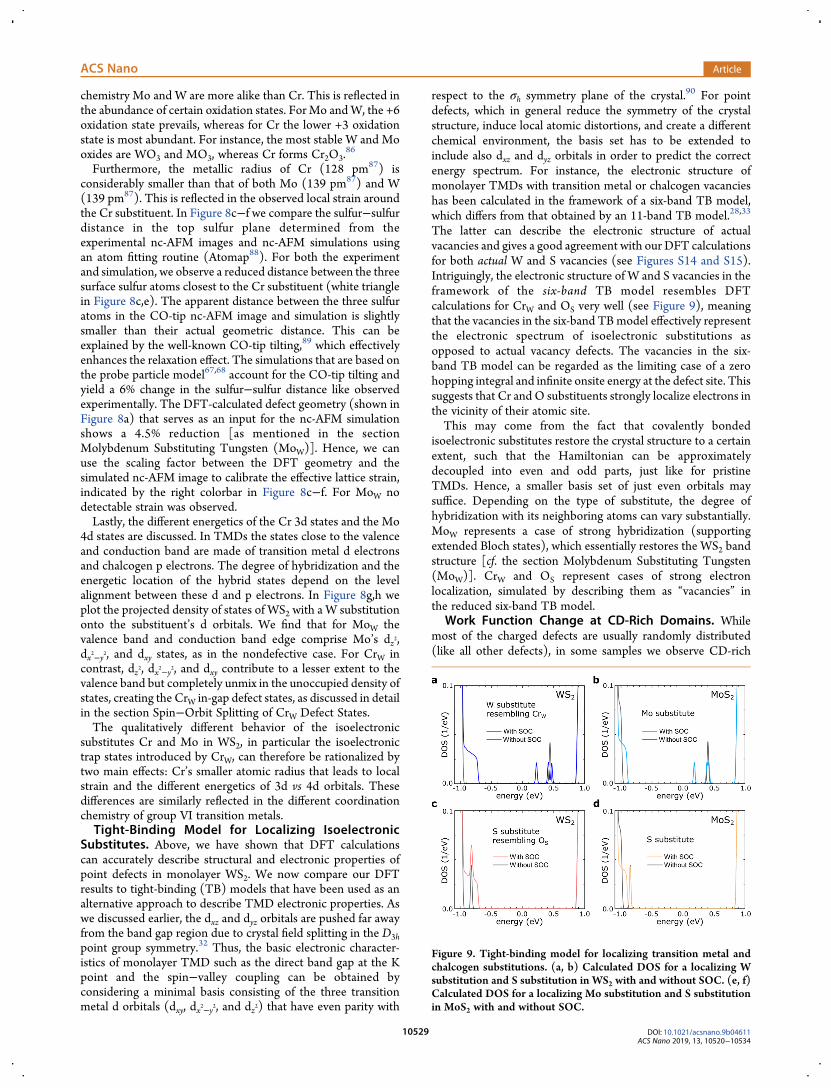
Furthermore, the metallic radius of Cr (128 pm87) isconsiderably smaller than that of both Mo (139 pm87) and W(139 pm87). This is reflected in the observed local strain aroundthe Cr substituent. In Figure 8c−f we compare the sulfur−sulfurdistance in the top sulfur plane determined from theexperimental nc-AFM images and nc-AFM simulations usingan atom fitting routine (Atomap88). For both the experimentand simulation, we observe a reduced distance between the threesurface sulfur atoms closest to the Cr substituent (white trianglein Figure 8c,e). The apparent distance between the three sulfuratoms in the CO-tip nc-AFM image and simulation is slightlysmaller than their actual geometric distance. This can beexplained by the well-known CO-tip tilting,89 which effectivelyenhances the relaxation effect. The simulations that are based onthe probe particle model67,68 account for the CO-tip tilting andyield a 6% change in the sulfur−sulfur distance like observedexperimentally. The DFT-calculated defect geometry (shown inFigure 8a) that serves as an input for the nc-AFM simulationshows a 4.5% reduction [as mentioned in the sectionMolybdenum Substituting Tungsten (MoW)]. Hence, we canuse the scaling factor between the DFT geometry and thesimulated nc-AFM image to calibrate the effective lattice strain,indicated by the right colorbar in Figure 8c−f. For MoW nodetectable strain was observed.Lastly, the different energetics of the Cr 3d states and the Mo
4d states are discussed. In TMDs the states close to the valenceand conduction band are made of transition metal d electronsand chalcogen p electrons. The degree of hybridization and theenergetic location of the hybrid states depend on the levelalignment between these d and p electrons. In Figure 8g,h weplot the projected density of states of WS2 with a W substitutiononto the substituent’s d orbitals. We find that for MoW thevalence band and conduction band edge comprise Mo’s dz2,dx2−y2, and dxy states, as in the nondefective case. For CrW incontrast, dz2, dx2−y2, and dxy contribute to a lesser extent to thevalence band but completely unmix in the unoccupied density ofstates, creating the CrW in-gap defect states, as discussed in detailin the section Spin−Orbit Splitting of CrW Defect States.The qualitatively different behavior of the isoelectronic
substitutes Cr and Mo in WS2, in particular the isoelectronictrap states introduced by CrW, can therefore be rationalized bytwo main effects: Cr’s smaller atomic radius that leads to localstrain and the different energetics of 3d vs 4d orbitals. Thesedifferences are similarly reflected in the different coordinationchemistry of group VI transition metals.Tight-Binding Model for Localizing Isoelectronic
Substitutes. Above, we have shown that DFT calculationscan accurately describe structural and electronic properties ofpoint defects in monolayer WS2. We now compare our DFTresults to tight-binding (TB) models that have been used as analternative approach to describe TMD electronic properties. Aswe discussed earlier, the dxz and dyz orbitals are pushed far awayfrom the band gap region due to crystal field splitting in the D3hpoint group symmetry.32 Thus, the basic electronic character-istics of monolayer TMD such as the direct band gap at the Kpoint and the spin−valley coupling can be obtained byconsidering a minimal basis consisting of the three transitionmetal d orbitals (dxy, dx2−y2, and dz2) that have even parity with
respect to the σh symmetry plane of the crystal.90 For pointdefects, which in general reduce the symmetry of the crystalstructure, induce local atomic distortions, and create a differentchemical environment, the basis set has to be extended toinclude also dxz and dyz orbitals in order to predict the correctenergy spectrum. For instance, the electronic structure ofmonolayer TMDs with transition metal or chalcogen vacancieshas been calculated in the framework of a six-band TB model,which differs from that obtained by an 11-band TB model.28,33
The latter can describe the electronic structure of actualvacancies and gives a good agreement with our DFT calculationsfor both actual W and S vacancies (see Figures S14 and S15).Intriguingly, the electronic structure of W and S vacancies in theframework of the six-band TB model resembles DFTcalculations for CrW and OS very well (see Figure 9), meaningthat the vacancies in the six-band TBmodel effectively representthe electronic spectrum of isoelectronic substitutions asopposed to actual vacancy defects. The vacancies in the six-band TB model can be regarded as the limiting case of a zerohopping integral and infinite onsite energy at the defect site. Thissuggests that Cr and O substituents strongly localize electrons inthe vicinity of their atomic site.This may come from the fact that covalently bonded
isoelectronic substitutes restore the crystal structure to a certainextent, such that the Hamiltonian can be approximatelydecoupled into even and odd parts, just like for pristineTMDs. Hence, a smaller basis set of just even orbitals maysuffice. Depending on the type of substitute, the degree ofhybridization with its neighboring atoms can vary substantially.MoW represents a case of strong hybridization (supportingextended Bloch states), which essentially restores the WS2 bandstructure [cf. the section Molybdenum Substituting Tungsten(MoW)]. CrW and OS represent cases of strong electronlocalization, simulated by describing them as “vacancies” inthe reduced six-band TB model.
Work Function Change at CD-Rich Domains. Whilemost of the charged defects are usually randomly distributed(like all other defects), in some samples we observe CD-rich
Figure 9. Tight-binding model for localizing transition metal andchalcogen substitutions. (a, b) Calculated DOS for a localizing Wsubstitution and S substitution in WS2 with and without SOC. (e, f)Calculated DOS for a localizing Mo substitution and S substitutionin MoS2 with and without SOC.
ACS Nano Article
DOI: 10.1021/acsnano.9b04611ACS Nano 2019, 13, 10520−10534
10529
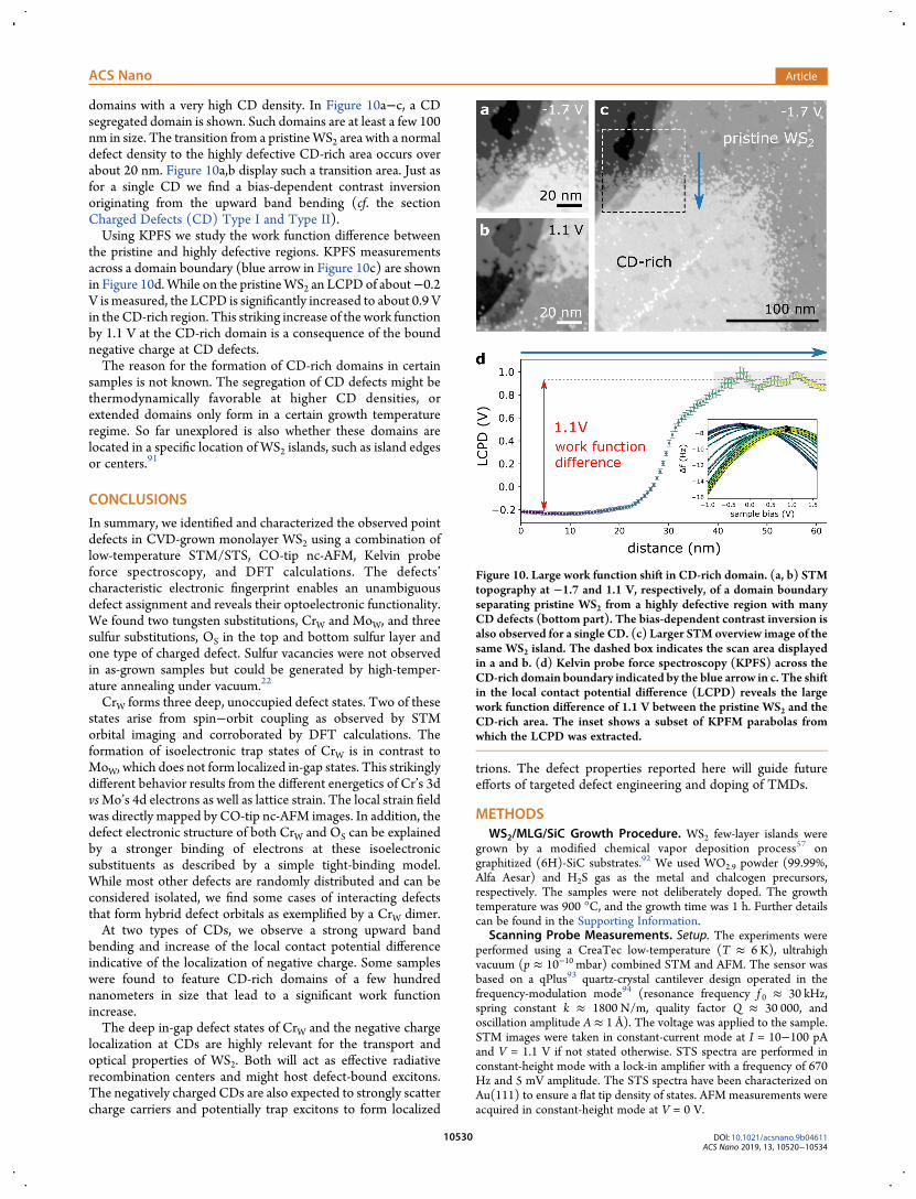
domains with a very high CD density. In Figure 10a−c, a CDsegregated domain is shown. Such domains are at least a few 100nm in size. The transition from a pristineWS2 area with a normaldefect density to the highly defective CD-rich area occurs overabout 20 nm. Figure 10a,b display such a transition area. Just asfor a single CD we find a bias-dependent contrast inversionoriginating from the upward band bending (cf. the sectionCharged Defects (CD) Type I and Type II).Using KPFS we study the work function difference between
the pristine and highly defective regions. KPFS measurementsacross a domain boundary (blue arrow in Figure 10c) are shownin Figure 10d.While on the pristineWS2 an LCPD of about−0.2V ismeasured, the LCPD is significantly increased to about 0.9 Vin the CD-rich region. This striking increase of the work functionby 1.1 V at the CD-rich domain is a consequence of the boundnegative charge at CD defects.The reason for the formation of CD-rich domains in certain
samples is not known. The segregation of CD defects might bethermodynamically favorable at higher CD densities, orextended domains only form in a certain growth temperatureregime. So far unexplored is also whether these domains arelocated in a specific location of WS2 islands, such as island edgesor centers.91
CONCLUSIONS
In summary, we identified and characterized the observed pointdefects in CVD-grown monolayer WS2 using a combination oflow-temperature STM/STS, CO-tip nc-AFM, Kelvin probeforce spectroscopy, and DFT calculations. The defects’characteristic electronic fingerprint enables an unambiguousdefect assignment and reveals their optoelectronic functionality.We found two tungsten substitutions, CrW and MoW, and threesulfur substitutions, OS in the top and bottom sulfur layer andone type of charged defect. Sulfur vacancies were not observedin as-grown samples but could be generated by high-temper-ature annealing under vacuum.22
CrW forms three deep, unoccupied defect states. Two of thesestates arise from spin−orbit coupling as observed by STMorbital imaging and corroborated by DFT calculations. Theformation of isoelectronic trap states of CrW is in contrast toMoW, which does not form localized in-gap states. This strikinglydifferent behavior results from the different energetics of Cr’s 3dvsMo’s 4d electrons as well as lattice strain. The local strain fieldwas directly mapped by CO-tip nc-AFM images. In addition, thedefect electronic structure of both CrW and OS can be explainedby a stronger binding of electrons at these isoelectronicsubstituents as described by a simple tight-binding model.While most other defects are randomly distributed and can beconsidered isolated, we find some cases of interacting defectsthat form hybrid defect orbitals as exemplified by a CrW dimer.At two types of CDs, we observe a strong upward band
bending and increase of the local contact potential differenceindicative of the localization of negative charge. Some sampleswere found to feature CD-rich domains of a few hundrednanometers in size that lead to a significant work functionincrease.The deep in-gap defect states of CrW and the negative charge
localization at CDs are highly relevant for the transport andoptical properties of WS2. Both will act as effective radiativerecombination centers and might host defect-bound excitons.The negatively charged CDs are also expected to strongly scattercharge carriers and potentially trap excitons to form localized
trions. The defect properties reported here will guide futureefforts of targeted defect engineering and doping of TMDs.
METHODSWS2/MLG/SiC Growth Procedure. WS2 few-layer islands were
grown by a modified chemical vapor deposition process57 ongraphitized (6H)-SiC substrates.92 We used WO2.9 powder (99.99%,Alfa Aesar) and H2S gas as the metal and chalcogen precursors,respectively. The samples were not deliberately doped. The growthtemperature was 900 °C, and the growth time was 1 h. Further detailscan be found in the Supporting Information.
Scanning Probe Measurements. Setup. The experiments wereperformed using a CreaTec low-temperature (T ≈ 6 K), ultrahighvacuum (p ≈ 10−10 mbar) combined STM and AFM. The sensor wasbased on a qPlus93 quartz-crystal cantilever design operated in thefrequency-modulation mode94 (resonance frequency f 0 ≈ 30 kHz,spring constant k ≈ 1800 N/m, quality factor Q ≈ 30 000, andoscillation amplitude A ≈ 1 Å). The voltage was applied to the sample.STM images were taken in constant-current mode at I = 10−100 pAand V = 1.1 V if not stated otherwise. STS spectra are performed inconstant-height mode with a lock-in amplifier with a frequency of 670Hz and 5 mV amplitude. The STS spectra have been characterized onAu(111) to ensure a flat tip density of states. AFMmeasurements wereacquired in constant-height mode at V = 0 V.
Figure 10. Large work function shift in CD-rich domain. (a, b) STMtopography at −1.7 and 1.1 V, respectively, of a domain boundaryseparating pristine WS2 from a highly defective region with manyCD defects (bottom part). The bias-dependent contrast inversion isalso observed for a single CD. (c) Larger STMoverview image of thesame WS2 island. The dashed box indicates the scan area displayedin a and b. (d) Kelvin probe force spectroscopy (KPFS) across theCD-rich domain boundary indicated by the blue arrow in c. The shiftin the local contact potential difference (LCPD) reveals the largework function difference of 1.1 V between the pristine WS2 and theCD-rich area. The inset shows a subset of KPFM parabolas fromwhich the LCPD was extracted.
ACS Nano Article
DOI: 10.1021/acsnano.9b04611ACS Nano 2019, 13, 10520−10534
10530
Sample and Tip Preparation. The CVD-grown WS2/Gr/SiC wasannealed in vacuo at about 250 °C for 30 min. We used focused ionbeam cut PtIr tips or chemically etched W tips that were sharpened byrepeated indentations into a Au substrate. A CO tip was created bypicking up a single CO molecule from the Au(111) surface.62,63 Boththe Au(111) and the WS2/Gr/SiC were mounted on the same sampleholder.Density-Functional Theory Calculations. We performed first-
principles DFT calculations using Quantum-Espresso.95,96 We used thePBE generalized gradient approximation97 for the exchange−correlation functional with scalar and fully relativistic optimizednorm-conserving Vanderbilt (ONCV) pseudopotentials from Pseudo-Dojo library.98 We used the experimental lattice parameter of 3.15 Å99
and a 5 × 5 or 7 × 7 WS2 supercell with a ∼15 Å vacuum region. Weapplied a plane wave cutoff energy of 100 Ry and 4 × 4 × 1 (3 × 3) k-point sampling for a 5 × 5 (7 × 7) supercell. We simulated the orbitalcharacter by means of integrated local density of states. More details onthe effect of the DFT functional and lattice constant can be found in theSupporting Information.Tight-Binding Model. The tight-binding calculations are imple-
mented following ref 28. We consider single layers of WS2 containing2400 × 2400 atoms, with periodic boundary conditions. The electronicband structure is considered from a tight-binding model that containssix-bands: three W 5d orbitals (dxy, dx2−y2, and dz2) and three S 3porbitals (px, py, and pz).
100 Intra-atomic spin−orbit coupling is includedin the model. The density of states and quasi-eigenstates are obtainednumerically from the tight-binding propagation method.101 In thesimulations, localizing substitutions are mimicked by randomlyremoving sulfur or tungsten atoms without lattice relaxation. Moredetails on the tight-binding model can be found in the SupportingInformation.
ASSOCIATED CONTENT*S Supporting InformationThe Supporting Information is available free of charge on theACS Publications website at DOI: 10.1021/acsnano.9b04611.
CVD growth details of WS2 on Gr/SiC, lattice siteidentification for MoW and CD type II, CO-tip nc-AFMsimulations of WS2 defects, DFT calculations of othersubstitutional defects considered, details on the tight-binding calculations (PDF)
AUTHOR INFORMATIONCorresponding Authors*E-mail: [email protected].*E-mail: [email protected].*E-mail: [email protected] Schuler: 0000-0002-9641-0340Christoph Kastl: 0000-0001-5309-618XKatherine A. Cochrane: 0000-0001-8268-2938Sivan Refaely-Abramson: 0000-0002-7031-8327Nicholas J. Borys: 0000-0001-5434-1191Roland J. Koch: 0000-0001-5748-8463Adam M. Schwartzberg: 0000-0001-6335-0719NotesThe authors declare no competing financial interest.
ACKNOWLEDGMENTSWe would like to thank Thomas Seyller for help preparing thegraphene on SiC substrates and Prokop Hapala for support withsetting up the AFM simulations. This work was performed at theMolecular Foundry supported by the Office of Science, Office ofBasic Energy Sciences, of the U.S. Department of Energy under
Contract No. DE-AC02-05CH11231. B.S. appreciates supportfrom the Swiss National Science Foundation under projectnumber P2SKP2_171770. J.-H.L. and J.B.N. were supported bythe Theory FWP, which is funded by the Department of Energy,Office of Science, Basic Energy Sciences, Materials Sciences andEngineering Division, under Contract No. DE-AC02-05CH11231. C.K. gratefully acknowledges support by theBavaria California Technology Center (BaCaTeC) and theInternational Graduate School of Science and Engineering(IGSSE) through project “CommOnChip”. A.W.-B. wassupported by the U.S. Department of Energy Early CareerAward. S.Y. acknowledges the financial support by the NationalKey R&D Program of China (Grant No. 2018FYA0305800)and computational resources provided by the SupercomputingCenter of Wuhan University.
REFERENCES(1) Lin, Z.; Carvalho, B. R.; Kahn, E.; Lv, R.; Rao, R.; Terrones, H.;Pimenta, M. A.; Terrones, M. Defect Engineering of Two-DimensionalTransition Metal Dichalcogenides. 2D Mater. 2016, 3, 022002.(2) Novoselov, K.; Mishchenko, A.; Carvalho, A.; Neto, A. C. 2DMaterials and Van Der Waals Heterostructures. Science 2016, 353,aac9439.(3) Manzeli, S.; Ovchinnikov, D.; Pasquier, D.; Yazyev, O. V.; Kis, A.2D Transition Metal Dichalcogenides.Nat. Rev. Mater. 2017, 2, 17033.(4) Mak, K. F.; Shan, J. Photonics and Optoelectronics of 2DSemiconductor Transition Metal Dichalcogenides. Nat. Photonics2016, 10, 216.(5) Das, S.; Robinson, J. A.; Dubey, M.; Terrones, H.; Terrones, M.Beyond Graphene: Progress in Novel Two-Dimensional Materials andVan Der Waals Solids. Annu. Rev. Mater. Res. 2015, 45, 1−27.(6) Li, Y.; Chernikov, A.; Zhang, X.; Rigosi, A.; Hill, H. M.; van derZande, A. M.; Chenet, D. A.; Shih, E.-M.; Hone, J.; Heinz, T. F.Measurement of the Optical Dielectric Function of MonolayerTransition-Metal Dichalcogenides: MoS2, MoSe2, WS2, and WSe2.Phys. Rev. B: Condens. Matter Mater. Phys. 2014, 90, 205422.(7) Xu, X.; Yao, W.; Xiao, D.; Heinz, T. F. Spin and Pseudospins inLayered Transition Metal Dichalcogenides. Nat. Phys. 2014, 10, 343.(8) Schaibley, J. R.; Yu, H.; Clark, G.; Rivera, P.; Ross, J. S.; Seyler, K.L.; Yao,W.; Xu, X. Valleytronics in 2DMaterials.Nat. Rev. Mater. 2016,1, 16055.(9) Zhu, Z.; Cheng, Y.; Schwingenschlogl, U. Giant Spin-Orbit-Induced Spin Splitting in Two-Dimensional Transition-MetalDichalcogenide Semiconductors. Phys. Rev. B: Condens. Matter Mater.Phys. 2011, 84, 153402.(10) Ugeda,M.M.; Bradley, A. J.; Shi, S.-F.; Felipe, H.; Zhang, Y.; Qiu,D. Y.; Ruan, W.; Mo, S.-K.; Hussain, Z.; Shen, Z.-X.; et al. GiantBandgap Renormalization and Excitonic Effects in a MonolayerTransition Metal Dichalcogenide Semiconductor. Nat. Mater. 2014,13, 1091−1095.(11) Yao, K.; Yan, A.; Kahn, S.; Suslu, A.; Liang, Y.; Barnard, E. S.;Tongay, S.; Zettl, A.; Borys, N. J.; Schuck, P. J. Optically DiscriminatingCarrier-Induced Quasiparticle Band Gap and Exciton EnergyRenormalization in Monolayer MoS2. Phys. Rev. Lett. 2017, 119,087401.(12) Qiu, D. Y.; da Jornada, F. H.; Louie, S. G. Optical Spectrum ofMoS2: Many-body Effects and Diversity of Exciton States. Phys. Rev.Lett. 2013, 111, 216805.(13) Yang, J.-H.; Yakobson, B. Dimensionality-Suppressed ChemicalDoping in 2D Semiconductors: The Cases of Phosphorene, MoS2, andReS2 from First-Principles. arXiv:1711.05094, 2017.(14) Aharonovich, I.; Englund, D.; Toth, M. Solid-State Single-Photon Emitters. Nat. Photonics 2016, 10, 631.(15) Gupta, S.; Yang, J.-H.; Yakobson, B. I. Two-Level QuantumSystems in Two-Dimensional Materials for Single Photon Emission.Nano Lett. 2019, 19, 408.
ACS Nano Article
DOI: 10.1021/acsnano.9b04611ACS Nano 2019, 13, 10520−10534
10531
(16) Zhou, W.; Zou, X.; Najmaei, S.; Liu, Z.; Shi, Y.; Kong, J.; Lou, J.;Ajayan, P. M.; Yakobson, B. I.; Idrobo, J.-C. Intrinsic Structural 16.Defects in Monolayer Molybdenum Disulfide. Nano Lett. 2013, 13,2615−2622.(17) Barja, S.; Wickenburg, S.; Liu, Z.-F.; Zhang, Y.; Ryu, H.; Ugeda,M. M.; Hussain, Z.; Shen, Z.-X.; Mo, S.-K.; Wong, E.; et al. ChargeDensity Wave Order in 1D Mirror Twin Boundaries of Single-LayerMoSe2. Nat. Phys. 2016, 12, 751−756.(18) Wang, S.; Robertson, A.; Warner, J. H. Atomic Structure ofDefects and Dopants in 2D Layered Transition Metal Dichalcogenides.Chem. Soc. Rev. 2018, 47, 6764−6794.(19) Lin, Y.-C.; Bjorkman, T.; Komsa, H.-P.; Teng, P.-Y.; Yeh, C.-H.;Huang, F.-S.; Lin, K.-H.; Jadczak, J.; Huang, Y.-S.; Chiu, P.-W.; et al.Three-Fold Rotational Defects in Two-Dimensional Transition MetalDichalcogenides. Nat. Commun. 2015, 6, 6736.(20) Komsa, H.-P.; Kotakoski, J.; Kurasch, S.; Lehtinen, O.; Kaiser, U.;Krasheninnikov, A. V. Two-Dimensional Transition Metal Dichalco-genides Under Electron Irradiation: Defect Production and Doping.Phys. Rev. Lett. 2012, 109, 035503.(21) Klein, J.; Kuc, A.; Nolinder, A.; Altzschner, M.; Wierzbowski, J.;Sigger, F.; Kreupl, F.; Finley, J.; Wurstbauer, U.; Holleitner, A.; et al.Robust Valley Polarization of Helium Ion Modified Atomically ThinMoS2. 2D Mater. 2018, 5, 011007.(22) Schuler, B.; Qiu, D. Y.; Refaely-Abramson, S.; Kastl, C.; Chen, C.T.; Barja, S.; Koch, R. J.; Ogletree, D. F.; Aloni, S.; Schwartzberg, A. M.;et al. Large Spin-Orbit Splitting of Deep In-Gap Defect States ofEngineered Sulfur Vacancies in Monolayer WS2. Phys. Rev. Lett. 2019,123, 076801.(23) Hildebrand, B.; Didiot, C.; Novello, A. M.; Monney, G.; Scarfato,A.; Ubaldini, A.; Berger, H.; Bowler, D.; Renner, C.; Aebi, P. DopingNature of Native Defects in 1T-TiSe2. Phys. Rev. Lett. 2014, 112,197001.(24) Gao, J.; Kim, Y. D.; Liang, L.; Idrobo, J. C.; Chow, P.; Tan, J.; Li,B.; Li, L.; Sumpter, B. G.; Lu, T.-M.; et al. Transition-Metal SubstitutionDoping in Synthetic Atomically Thin Semiconductors. Adv. Mater.2016, 28, 9735−9743.(25) Barja, S.; Refaely-Abramson, S.; Schuler, B.; Qiu, D. Y.; Pulkin,A.; Wickenburg, S.; Ryu, H.; Ugeda, M. M.; Kastl, C.; Chen, C.; et al.Identifying Substitutional Oxygen as a Prolific Point Defect inMonolayer Transition Metal Dichalcogenides with Experiment andTheory. Nat. Commun. 2019, 10, 3382.(26) Van Der Zande, A. M.; Huang, P. Y.; Chenet, D. A.; Berkelbach,T. C.; You, Y.; Lee, G.-H.; Heinz, T. F.; Reichman, D. R.; Muller, D. A.;Hone, J. C. Grains and Grain Boundaries in Highly CrystallineMonolayer Molybdenum Disulphide. Nat. Mater. 2013, 12, 554−561.(27) Le, D.; Rahman, T. S. Joined Edges in MoS2: Metallic and Half-Metallic Wires. J. Phys.: Condens. Matter 2013, 25, 312201.(28) Yuan, S.; Roldan, R.; Katsnelson, M.; Guinea, F. Effect of PointDefects on the Optical and Transport Properties of MoS2 and WS2.Phys. Rev. B: Condens. Matter Mater. Phys. 2014, 90, 041402.(29) Lehtinen, O.; Komsa, H.-P.; Pulkin, A.; Whitwick, M. B.; Chen,M.-W.; Lehnert, T.; Mohn, M. J.; Yazyev, O. V.; Kis, A.; Kaiser, U.; et al.Atomic Scale Microstructure and Properties of Se-Deficient Two-Dimensional MoSe2. ACS Nano 2015, 9, 3274−3283.(30) Komsa, H.-P.; Krasheninnikov, A. V. Native Defects in Bulk andMonolayer MoS2 from First Principles. Phys. Rev. B: Condens. MatterMater. Phys. 2015, 91, 125304.(31) Haldar, S.; Vovusha, H.; Yadav, M. K.; Eriksson, O.; Sanyal, B.Systematic Study of Structural, Electronic, and Optical Properties ofAtomic-Scale Defects in the Two-Dimensional Transition MetalDichalcogenides MX2 (M= Mo, W; X= S, Se, Te). Phys. Rev. B:Condens. Matter Mater. Phys. 2015, 92, 235408.(32) Li, W.-F.; Fang, C.; van Huis, M. A. Strong Spin-Orbit Splittingand Magnetism of Point Defect States in Monolayer WS2. Phys. Rev. B:Condens. Matter Mater. Phys. 2016, 94, 195425.(33) Khan, M.; Erementchouk, M.; Hendrickson, J.; Leuenberger, M.N. Electronic andOptical Properties of VacancyDefects in Single-LayerTransition Metal Dichalcogenides. Phys. Rev. B: Condens. Matter Mater.Phys. 2017, 95, 245435.
(34) Naik, M. H.; Jain, M. Substrate Screening Effects on theQuasiparticle Band Gap and Defect Charge Transition Levels in MoS2.Phys. Rev. Materials 2018, 2, 084002.(35) Qiu, H.; Xu, T.; Wang, Z.; Ren, W.; Nan, H.; Ni, Z.; Chen, Q.;Yuan, S.; Miao, F.; Song, F.; et al. Hopping Transport Through Defect-Induced Localized States in Molybdenum Disulphide. Nat. Commun.2013, 4, 2642.(36) Tongay, S.; Suh, J.; Ataca, C.; Fan, W.; Luce, A.; Kang, J. S.; Liu,J.; Ko, C.; Raghunathanan, R.; Zhou, J.; et al. Defects ActivatedPhotoluminescence in Two-Dimensional Semiconductors: InterplayBetween Bound, Charged, and Free Excitons. Sci. Rep. 2013, 3, 2657.(37) Chow, P. K.; Jacobs-Gedrim, R. B.; Gao, J.; Lu, T.-M.; Yu, B.;Terrones, H.; Koratkar, N. Defect-Induced Photoluminescence inMonolayer Semiconducting Transition Metal Dichalcogenides. ACSNano 2015, 9, 1520−1527.(38) Carozo, V.; Wang, Y.; Fujisawa, K.; Carvalho, B. R.; McCreary,A.; Feng, S.; Lin, Z.; Zhou, C.; Perea-Lopez, N.; Elías, A. L.; et al.Optical Identification of Sulfur Vacancies: Bound Excitons at the Edgesof Monolayer Tungsten Disulfide. Sci. Adv. 2017, 3, No. e1602813.(39) Saigal, N.; Ghosh, S. Evidence for Two Distinct Defect RelatedLuminescence Features in Monolayer MoS2. Appl. Phys. Lett. 2016,109, 122105.(40) He, Y.-M.; Clark, G.; Schaibley, J. R.; He, Y.; Chen, M.-C.; Wei,Y.-J.; Ding, X.; Zhang, Q.; Yao, W.; Xu, X.; et al. Single QuantumEmitters in Monolayer Semiconductors. Nat. Nanotechnol. 2015, 10,497−502.(41) Chakraborty, C.; Kinnischtzke, L.; Goodfellow, K.M.; Beams, R.;Vamivakas, A. N. Voltage-Controlled Quantum Light from anAtomically Thin Semiconductor.Nat. Nanotechnol. 2015, 10, 507−511.(42) Koperski, M.; Nogajewski, K.; Arora, A.; Cherkez, V.; Mallet, P.;Veuillen, J.-Y.; Marcus, J.; Kossacki, P.; Potemski, M. Single PhotonEmitters in Exfoliated WSe2 Structures. Nat. Nanotechnol. 2015, 10,503−506.(43) Srivastava, A.; Sidler, M.; Allain, A. V.; Lembke, D. S.; Kis, A.;Imamoglu, A. Optically Active QuantumDots inMonolayerWSe2.Nat.Nanotechnol. 2015, 10, 491−496.(44) Li, G.; Zhang, D.; Qiao, Q.; Yu, Y.; Peterson, D.; Zafar, A.;Kumar, R.; Curtarolo, S.; Hunte, F.; Shannon, S.; et al. All the CatalyticActive Sites of MoS2 for Hydrogen Evolution. J. Am. Chem. Soc. 2016,138, 16632−16638.(45) Li, H.; Tsai, C.; Koh, A. L.; Cai, L.; Contryman, A.W.; Fragapane,A. H.; Zhao, J.; Han, H. S.; Manoharan, H. C.; Abild-Pedersen, F.; et al.Activating and Optimizing MoS2 Basal Planes for Hydrogen EvolutionThrough the Formation of Strained Sulphur Vacancies. Nat. Mater.2016, 15, 48.(46) Hong, J.; Jin, C.; Yuan, J.; Zhang, Z. Atomic Defects in Two-Dimensional Materials: From Single-Atom Spectroscopy to Function-alities in Opto-/Electronics, Nanomagnetism, and Catalysis. Adv.Mater. 2017, 29, 1606434(47) Zhang, W.; Li, X.; Jiang, T.; Song, J.; Lin, Y.; Zhu, L.; Xu, X. CVDSynthesis of Mo1−xWxS2 andMoS2(1−x)Se2x Alloy Monolayers Aimed atTuning the Bandgap of Molybdenum Disulfide. Nanoscale 2015, 7,13554−13560.(48) Zhang, M.; Wu, J.; Zhu, Y.; Dumcenco, D. O.; Hong, J.; Mao, N.;Deng, S.; Chen, Y.; Yang, Y.; Jin, C.; et al. Two-DimensionalMolybdenum Tungsten Diselenide Alloys: Photoluminescence,Raman Scattering, and Electrical Transport. ACS Nano 2014, 8,7130−7137.(49) Tongay, S.; Narang, D. S.; Kang, J.; Fan, W.; Ko, C.; Luce, A. V.;Wang, K. X.; Suh, J.; Patel, K.; Pathak, V.; et al. Two-DimensionalSemiconductor Alloys: Monolayer Mo1−xWxSe2. Appl. Phys. Lett. 2014,104, 012101.(50) Suh, J.; Tan, T. L.; Zhao,W.; Park, J.; Lin, D.-Y.; Park, T.-E.; Kim,J.; Jin, C.; Saigal, N.; Ghosh, S.; et al. Reconfiguring Crystal andElectronic Structures of MoS2 by Substitutional Doping.Nat. Commun.2018, 9, 199.(51) Hong, J.; Hu, Z.; Probert, M.; Li, K.; Lv, D.; Yang, X.; Gu, L.;Mao, N.; Feng, Q.; Xie, L.; et al. Exploring Atomic Defects inMolybdenum Disulphide Monolayers. Nat. Commun. 2015, 6, 6293.
ACS Nano Article
DOI: 10.1021/acsnano.9b04611ACS Nano 2019, 13, 10520−10534
10532
(52) Liu, X.; Balla, I.; Bergeron, H.; Hersam, M. C. Point Defects andGrain Boundaries in Rotationally Commensurate MoS2 on EpitaxialGraphene. J. Phys. Chem. C 2016, 120, 20798−20805.(53) Zhang, S.;Wang, C.-G.; Li, M.-Y.; Huang, D.; Li, L.-J.; Ji, W.;Wu,S. Defect Structure of Localized Excitons in a WSe2 Monolayer. Phys.Rev. Lett. 2017, 119, 046101.(54) Lin, Y.-C.; Jariwala, B.; Bersch, B. M.; Xu, K.; Nie, Y.; Wang, B.;Eichfeld, S. M.; Zhang, X.; Choudhury, T. H.; Pan, Y.; et al. RealizingLarge-Scale, Electronic-Grade Two-Dimensional Semiconductors.ACSNano 2018, 12, 965−975.(55) Kobayashi, Y.; Sasaki, S.; Mori, S.; Hibino, H.; Liu, Z.; Watanabe,K.; Taniguchi, T.; Suenaga, K.; Maniwa, Y.; Miyata, Y. Growth andOptical Properties of High-Quality Monolayer WS2 on Graphite. ACSNano 2015, 9, 4056−4063.(56) Forti, S.; Rossi, A.; Buch, H.; Cavallucci, T.; Bisio, F.; Sala, A.;Mentes, T. O.; Locatelli, A.; Magnozzi, M.; Canepa, M.; et al. ElectronicProperties of Single-Layer Tungsten Disulfide on Epitaxial Grapheneon Silicon Carbide. Nanoscale 2017, 9, 16412.(57) Kastl, C.; Chen, C.; Koch, R. J.; Schuler, B.; Kuykendall, T.;Bostwick, A.; Jozwiak, C.; Seyller, T.; Rotenberg, E.; Weber-Bargioni,A.; et al. Multimodal Spectromicroscopy of MonolayerWS2 Enabled byUltra-Clean van der Waals Epitaxy. 2D Mater. 2018, 5, 045010.(58) Kastl, C.; Chen, C. T.; Kuykendall, T.; Shevitski, B.; Darlington,T. P.; Borys, N. J.; Krayev, A.; Schuck, P. J.; Aloni, S.; Schwartzberg, A.M. The Important Role of Water in Growth of Monolayer TransitionMetal Dichalcogenides. 2D Mater. 2017, 4, 021024.(59) Ulstrup, S.; Giusca, C. E.; Miwa, J. A.; Sanders, C. E.; Browning,A.; Dudin, P.; Cacho, C.; Kazakova, O.; Gaskill, D. K.; Myers-Ward, R.L.; et al. Nanoscale Mapping of Quasiparticle Band Alignment. Nat.Commun. 2019, 10, 3283.(60) Riedl, C.; Coletti, C.; Iwasaki, T.; Zakharov, A.; Starke, U. Quasi-Free-Standing Epitaxial Graphene on SiC Obtained by HydrogenIntercalation. Phys. Rev. Lett. 2009, 103, 246804.(61) Park, J. H.; Vishwanath, S.; Liu, X.; Zhou, H.; Eichfeld, S. M.;Fullerton-Shirey, S. K.; Robinson, J. A.; Feenstra, R. M.; Furdyna, J.;Jena, D.; et al. Scanning TunnelingMicroscopy and Spectroscopy of AirExposure Effects onMolecular Beam Epitaxy GrownWSe2 Monolayersand Bilayers. ACS Nano 2016, 10, 4258−4267.(62) Gross, L.; Mohn, F.; Moll, N.; Liljeroth, P.; Meyer, G. TheChemical Structure of a Molecule Resolved by Atomic ForceMicroscopy. Science 2009, 325, 1110.(63) Mohn, F.; Schuler, B.; Gross, L.; Meyer, G. Different Tips forHigh-Resolution AFM and STM Imaging of Single Molecules. Appl.Phys. Lett. 2013, 102, 073109.(64) Sanchez-Sanchez, C.; Gonzalez, C.; Jelinek, P.; Mendez, J.; DeAndres, P.; Martín-Gago, J. A.; Lopez, M. F. Understanding Atomic-Resolved STM Images on TiO2(110)-(1× 1) Surface by DFTCalculations. Nanotechnology 2010, 21, 405702.(65) Tumino, F.; Casari, C. S.; Passoni, M.; Russo, V.; Bassi, A. L.Pulsed Laser Deposition of Single-Layer MoS2 on Au(111): FromNanosized Crystals to Large-Area Films. Nanoscale Adv.. 2019, 1, 643.(66) Moll, N.; Gross, L.; Mohn, F.; Curioni, A.; Meyer, G. TheMechanisms Underlying the Enhanced Resolution of Atomic ForceMicroscopy with Functionalized Tips. New J. Phys. 2010, 12, 125020.(67) Hapala, P.; Kichin, G.; Wagner, C.; Tautz, F. S.; Temirov, R.;Jelínek, P. Mechanism of High-Resolution STM/AFM Imaging withFunctionalized Tips. Phys. Rev. B: Condens. Matter Mater. Phys. 2014,90, 085421.(68) Hapala, P.; Temirov, R.; Tautz, F. S.; Jelínek, P. Origin of High-Resolution IETS-STM Images of Organic Molecules with Function-alized Tips. Phys. Rev. Lett. 2014, 113, 226101.(69) Robertson, A. W.; Lin, Y.-C.; Wang, S.; Sawada, H.; Allen, C. S.;Chen, Q.; Lee, S.; Lee, G.-D.; Lee, J.; Han, S.; et al. Atomic Structureand Spectroscopy of Single Metal (Cr, V) Substitutional Dopants inMonolayer MoS2. ACS Nano 2016, 10, 10227−10236.(70) Karthikeyan, J.; Komsa, H.-P.; Batzill, M.; Krasheninnikov, A. V.Which Transition Metal Atoms Can Be Embedded Into Two-Dimensional Molybdenum Dichalcogenides and Add Magnetism?Nano Lett. 2019, 19, 4581.
(71) Le Quang, T.; Nogajewski, K.; Potemski, M.; Dau, M. T.; Jamet,M.; Mallet, P.; Veuillen, J. Band-Bending Induced by Charged Defectsand Edges of Atomically Thin Transition Metal Dichalcogenide Films.2D Mater. 2018, 5, 035034.(72) Addou, R.; Colombo, L.; Wallace, R. M. Surface Defects onNatural MoS2. ACS Appl. Mater. Interfaces 2015, 7, 11921−11929.(73) Mohn, F.; Gross, L.; Moll, N.; Meyer, G. Imaging the ChargeDistribution Within a Single Molecule. Nat. Nanotechnol. 2012, 7, 227.(74) Gross, L.; Mohn, F.; Liljeroth, P.; Repp, J.; Giessibl, F. J.; Meyer,G. Measuring the Charge State of an Adatom with Noncontact AtomicForce Microscopy. Science 2009, 324, 1428.(75) Aghajanian, M.; Mostofi, A. A.; Lischner, J. Tuning ElectronicProperties of Transition-Metal Dichalcogenides via Defect Charge. Sci.Rep. 2018, 8, 13611.(76) Schulz, F.; Ijas, M.; Drost, R.; Hamalainen, S. K.; Harju, A.;Seitsonen, A. P.; Liljeroth, P. Many-Body Transitions in a SingleMolecule Visualized by Scanning Tunnelling Microscopy. Nat. Phys.2015, 11, 229.(77) Yu, P.; Kocic, N.; Repp, J.; Siegert, B.; Donarini, A. ApparentReversal of Molecular Orbitals Reveals Entanglement. Phys. Rev. Lett.2017, 119, 056801.(78) Schoenaers, B.; Stesmans, A.; Afanas’ev, V. V. Nitrogen Acceptorin 2H-Polytype Synthetic MoS2 Assessed by Multifrequency ElectronSpin Resonance. J. Vac. Sci. Technol., A 2018, 36, 05G503.(79) Azcatl, A.; Qin, X.; Prakash, A.; Zhang, C.; Cheng, L.; Wang, Q.;Lu, N.; Kim, M. J.; Kim, J.; Cho, K.; et al. Covalent Nitrogen Dopingand Compressive Strain inMoS2 by Remote N2 Plasma Exposure.NanoLett. 2016, 16, 5437−5443.(80) Tang, B.; Yu, Z. G.; Huang, L.; Chai, J.; Wong, S. L.; Deng, J.;Yang, W.; Gong, H.; Wang, S.; Ang, K.-W.; et al. Direct n- to p-TypeChannel Conversion in Monolayer/Few-Layer WS2 Field-EffectTransistors by Atomic Nitrogen Treatment. ACS Nano 2018, 12,2506−2513.(81) Zhang, F.; Lu, Y.; Schulman, D. S.; Zhang, T.; Fujisawa, K.; Lin,Z.; Lei, Y.; Elias, A. L.; Das, S.; Sinnott, S. B.; et al. Carbon Doping ofWS2 Monolayers: Bandgap Reduction and p-Type Doping Transport.Sci. Adv. 2019, 5, No. eaav5003.(82) Mak, K. F.; He, K.; Shan, J.; Heinz, T. F. Control of ValleyPolarization in Monolayer MoS2 by Optical Helicity. Nat. Nanotechnol.2012, 7, 494.(83) Coulson, C. A.; Kearsley, M. J. Colour Centres in IrradiatedDiamonds. I. Proc. R. Soc. London A 1957, 241, 433−454.(84) van der Heijden, J.; Kobayashi, T.; House, M. G.; Salfi, J.;Barraud, S.; Lavieville, R.; Simmons, M. Y.; Rogge, S. Readout andControl of the Spin-Orbit States of Two Coupled Acceptor Atoms in aSilicon Transistor. Sci. Adv. 2018, 4, No. eaat9199.(85) Klein, J.; Lorke, M.; Florian, M.; Sigger, F.; Sigl, L.; Rey, S.;Wierzbowski, J.; Cerne, J.; Muller, K.; Mitterreiter, E.; et al. Site-Selectively Generated Photon Emitters in Monolayer MoS2 Via LocalHelium Ion Irradiation. Nat. Commun. 2019, 10, 2755.(86) Fierro, J., Ed. Metal Oxides, 1st ed.; CRC Press, 2005.(87) Greenwood, N. N.; Earnshaw, A. Chemistry of the Elements, 2nded.; Elsevier, 2012.(88) Nord, M.; Vullum, P. E.; MacLaren, I.; Tybell, T.; Holmestad, R.Atomap: A New Software Tool for the Automated Analysis of AtomicResolution Images Using Two-Dimensional Gaussian Fitting. Adv.Struct. Chem. Imaging 2017, 3, 9.(89) Gross, L.; Mohn, F.; Moll, N.; Schuler, B.; Criado, A.; Guitian, E.;Pena, D.; Gourdon, A.; Meyer, G. Bond-Order Discrimination byAtomic Force Microscopy. Science 2012, 337, 1326.(90) Xiao, D.; Liu, G.-B.; Feng, W.; Xu, X.; Yao, W. Coupled Spin andValley Physics in Monolayers of MoS2 and Other Group-VIDichalcogenides. Phys. Rev. Lett. 2012, 108, 196802.(91) Bao, W.; Borys, N. J.; Ko, C.; Suh, J.; Fan, W.; Thron, A.; Zhang,Y.; Buyanin, A.; Zhang, J.; Cabrini, S.; et al. Visualizing NanoscaleExcitonic Relaxation Properties of Disordered Edges and GrainBoundaries in Monolayer Molybdenum Disulfide. Nat. Commun.2015, 6, 7993.
ACS Nano Article
DOI: 10.1021/acsnano.9b04611ACS Nano 2019, 13, 10520−10534
10533
(92) Emtsev, K. V.; Bostwick, A.; Horn, K.; Jobst, J.; Kellogg, G. L.;Ley, L.; McChesney, J. L.; Ohta, T.; Reshanov, S. A.; Rohrl, J.; et al.Towards Wafer-Size Graphene Layers by Atmospheric PressureGraphitization of Silicon Carbide. Nat. Mater. 2009, 8, 203.(93) Giessibl, F. J. High-Speed Force Sensor for Force Microscopyand Profilometry Utilizing aQuartz Tuning Fork.Appl. Phys. Lett. 1998,73, 3956.(94) Albrecht, T. R.; Grutter, P.; Horne, D.; Rugar, D. FrequencyModulation Detection Using High-Q Cantilevers for Enhanced ForceMicroscope Sensitivity. J. Appl. Phys. 1991, 69, 668−673.(95) Giannozzi, P.; Baroni, S.; Bonini, N.; Calandra, M.; Car, R.;Cavazzoni, C.; Ceresoli, D.; Chiarotti, G. L.; Cococcioni, M.; Dabo, I.;et al. QUANTUM ESPRESSO: A Modular and Open-Source SoftwareProject for Quantum Simulations of Materials. J. Phys.: Condens. Matter2009, 21, 395502.(96) Giannozzi, P.; Andreussi, O.; Brumme, T.; Bunau, O.; Nardelli,M. B.; Calandra, M.; Car, R.; Cavazzoni, C.; Ceresoli, D.; Cococcioni,M.; et al. Advanced Capabilities for Materials Modelling with QuantumESPRESSO. J. Phys.: Condens. Matter 2017, 29, 465901.(97) Perdew, J. P.; Burke, K.; Ernzerhof, M. Generalized GradientApproximation Made Simple. Phys. Rev. Lett. 1996, 77, 3865−3868.(98) Hamann, D. R. Optimized Norm-Conserving VanderbiltPseudopotentials. Phys. Rev. B: Condens. Matter Mater. Phys. 2013,88, 085117.(99) Schutte, W.; De Boer, J.; Jellinek, F. Crystal Structures ofTungsten Disulfide and Diselenide. J. Solid State Chem. 1987, 70, 207−209.(100) Cappelluti, E.; Roldan, R.; Silva-Guillen, J. A.; Ordejon, P.;Guinea, F. Tight-Binding Model and Direct-Gap/Indirect-GapTransition in Single-Layer and Multilayer MoS2. Phys. Rev. B: Condens.Matter Mater. Phys. 2013, 88, 075409.(101) Yuan, S.; De Raedt, H.; Katsnelson, M. I. Modeling ElectronicStructure and Transport Properties of Graphene with ResonantScattering Centers. Phys. Rev. B: Condens. Matter Mater. Phys. 2010,82, 115448.
ACS Nano Article
DOI: 10.1021/acsnano.9b04611ACS Nano 2019, 13, 10520−10534
10534