
Hot Test Experiment Design Considerations for a Backward ...
22
Hot Test Experiment Design Considerations for a Backward Wave Oscillator based on a Novel Slow Wave Structure Ushe Chipengo, Niru Nahar & John Volakis MURI Teleconference October 7 2016
Transcript of Hot Test Experiment Design Considerations for a Backward ...

Hot Test Experiment Design Considerations for a Backward Wave Oscillator based on a
Novel Slow Wave Structure
Ushe Chipengo, Niru Nahar & John Volakis
MURI Teleconference
October 7 2016
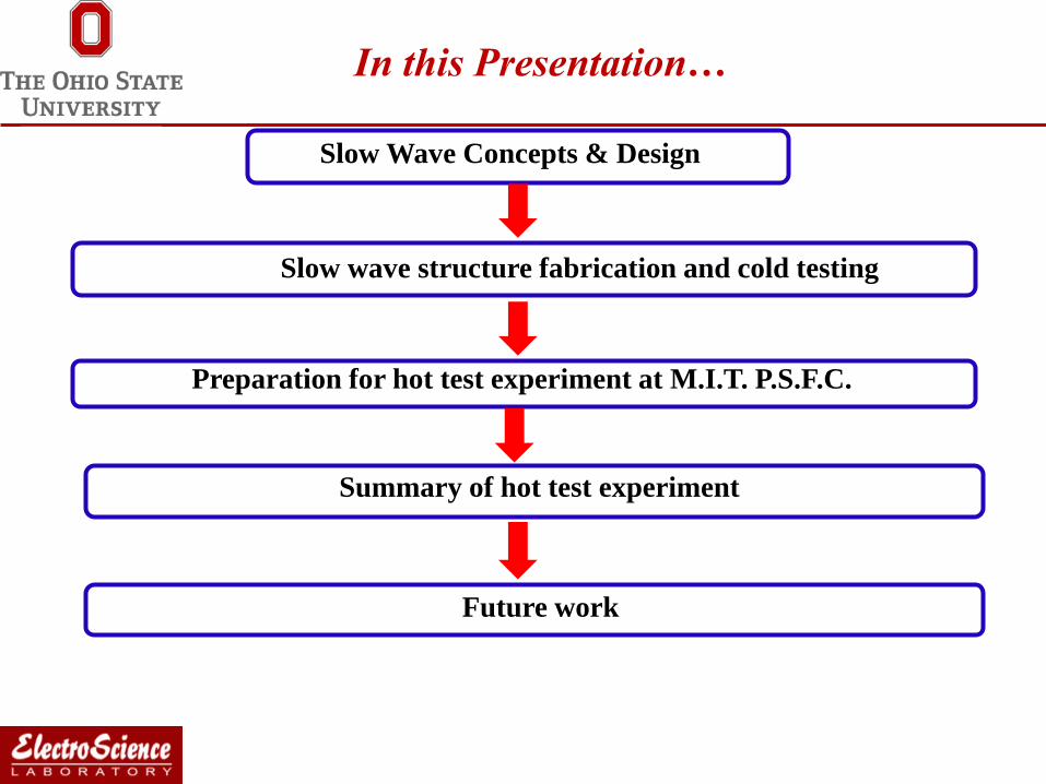
In this Presentation…
Slow Wave Concepts & Design
Slow wave structure fabrication and cold testing
Preparation for hot test experiment at M.I.T. P.S.F.C.
Summary of hot test experiment
Future work
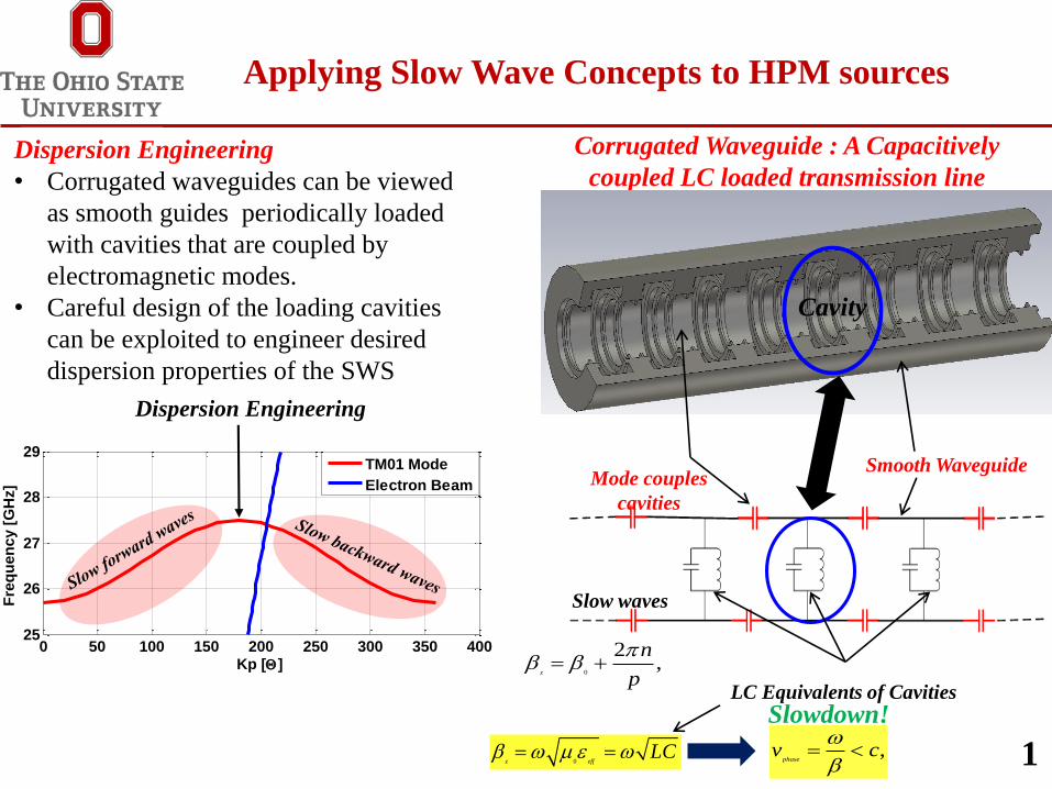
Applying Slow Wave Concepts to HPM sources
LC Equivalents of Cavities
0
2,
z
n
p
0z effLC ,
phasev c
Slowdown!
Smooth Waveguide
Corrugated Waveguide : A Capacitively
coupled LC loaded transmission line
Slow waves
Cavity
Dispersion Engineering
• Corrugated waveguides can be viewed
as smooth guides periodically loaded
with cavities that are coupled by
electromagnetic modes.
• Careful design of the loading cavities
can be exploited to engineer desired
dispersion properties of the SWS
0 50 100 150 200 250 300 350 40025
26
27
28
29
Kp []
Fre
qu
en
cy [
GH
z]
TM01 Mode
Electron Beam
Dispersion Engineering
Mode couples
cavities
1
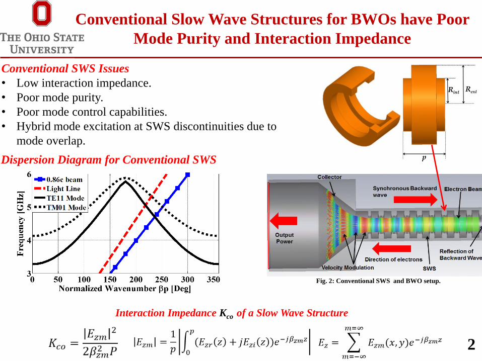
Conventional SWS Issues
• Low interaction impedance.
• Poor mode purity.
• Poor mode control capabilities.
• Hybrid mode excitation at SWS discontinuities due to
mode overlap.
Fig. 1: Dispersion Diagram for conventional SWS’s Fig. 2: Conventional SWS and BWO setup.
Conventional Slow Wave Structures for BWOs have Poor
Mode Purity and Interaction Impedance
Interaction Impedance Kco of a Slow Wave Structure
Dispersion Diagram for Conventional SWS
2
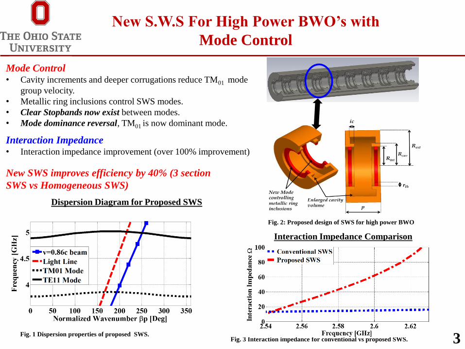
New S.W.S For High Power BWO’s with
Mode Control
Fig. 2: Proposed design of SWS for high power BWO
Fig. 3 Interaction impedance for conventional vs proposed SWS.Fig. 1 Dispersion properties of proposed SWS.
Dispersion Diagram for Proposed SWS
Interaction Impedance Comparison
Mode Control• Cavity increments and deeper corrugations reduce TM01 mode
group velocity.
• Metallic ring inclusions control SWS modes.
• Clear Stopbands now exist between modes.
• Mode dominance reversal, TM01 is now dominant mode.
Interaction Impedance• Interaction impedance improvement (over 100% improvement)
New SWS improves efficiency by 40% (3 section
SWS vs Homogeneous SWS)
3

Novel SWS Design leads to Excellent Mode Purity
Mode Purity
• Strong Ez fields increase interaction
impedance which improves BWO efficiency.
• Hybrid TE11-TM01 modes have weak Ez fields
(see fig. below).
• Hybrid modes can exist in a SWS if it is
excited at a frequency in the overlapping
passband region (a).
• Excellent mode purity is achieved through
passband overlap elimination and mode
dominance reversal (b).
4

Slow Wave Structure Fabrication
Fabricated Components
1) 2)
3) 4)
End Caps
Smooth
waveguide
section
6 SWS unit
cells
End Caps
Smooth
waveguide
section
Smooth
waveguide
Section
SWS Unit Cell
to be placed
inside
waveguide
Enlarged cavity
recessions
Metallic
ring
inclusions
Novel SWS Design
1) Entire SWS components include:
end caps, waveguide section and
unit cells.
2) Metallic ring insertion and cavity
recessions realization is achieved in
fabricated SWS unit cell.
3) End caps on both ends of the
waveguide create resonant cavity.
4) SWS unit cell is to be loaded into
smooth waveguide section
5

S11 Response of TM01 Mode
• 7 resonances corresponding to TM01 mode were observed
and their locations agree with simulated results .
• Resonances can be used to derive the dispersion curve of
the TM01 mode in SWS.
Excitation
probe
Loaded
waveguide
section
Vector
Network
Analyzer
6

0 60 120 180 240 300 360
2.55
2.6
2.65
2.7
2.75
Normalized Wave Number p [Deg]
Fre
qu
ency
[G
Hz]
Measured+ Synthetic Technique
HFSS
CST
0 pi/6 2pi/6 3pi/6 4pi/6 5pi/6 pi2.5
2.55
2.6
2.65
2.7
p [rad]F
req
uen
cy [
GH
z]
Measured
CST
HFSS
GHz Measured CST HFSS
2.551 2.552 2.567
2.566 2.561 2.574
2.588 2.583 2.594
2.618 2.614 2.622
2.651 2.644 2.649
2.674 2.666 2.668
2.684 2.674 2.675
𝒇𝟎𝒇𝝅𝟔
𝒇𝟐𝝅𝟔𝒇𝟑𝝅𝟔𝒇𝟒𝝅𝟔
𝒇𝟓𝝅𝟔
𝒇𝝅
TM01 Response : Measurements vs
Simulated Resonant Frequencies Location
• Results from measured resonances show
excellent agreement with commercial
software packages CST and HFSS.
Dispersion Curve
• Derived dispersion curve is in excellent
agreement with CST and HFSS
simulation results.
Resonance location:
Simulation vs
Measurement
TM01 Dispersion
Curve:
Simulation vs
Measurement
𝒇 =
𝒎=𝟎
∞
𝒂𝒎𝒄𝒐𝒔(𝒎𝜷𝑳)
7

Mode Dominance Reversal Validation(Complete Dispersion Curve )
Validation Process• S11 data confirm TM01 mode
dominance reversal.
• TM01 mode is the first mode to be
excited followed by a weaker TE11
mode.
• Bandgap between modes is also
observed clearly as expected.
• Excellent agreement between S11 data
and simulated dispersion curves is
observed.
Dispersion Curve of First 2 modes in
SWS
8

Preparations For Hot Test Experiment at M.I.T. PSFC:
Description and Challenges
Output
Couplers
OSU SWS
Placed HereElectron
Beam
Vacuum
Chamber Output RF Load
Collector
Fig. 1: Proposed experimental setup. OSU’s components will replace
the Metamaterial SWS used by MIT in previous experiments (CAD
drawing courtesy of Jason Hummelt (MIT))
Objective:
Experimentally validate the SWS design
properties and generate high power microwaves
at 30-40% efficiency.
Design Challenge:Adopt OSU’s novel SWS design to MIT’s existing
hot test infrastructure and test bed.
Specifically:
• Couple SWS mode to 490 kV, 84 A beam guided
by 0.15 T. (SWS was designed for 341 kV, 50 A &
1T).
• Adopt original endfire output power system to the
MIT dual rectangular waveguide system.
• Design mode converter for coupling generated
power to measurement waveguides.
• Fit the whole design in a 14 inch by 6 inch
vacuum space.
• Measured output power in TE01 mode using a
TE10 mode measurement system.
9

Preparations For Hot Test Experiment at M.I.T. PSFC:
Interaction Concept
Challenges
• Intense bunching permits transverse electron
trajectories that are permitted by available
magnetic field (0.18T).
• Electron beam starts to diverge due to intense
bunching.
• Transverse electron beam trajectories reduce
efficiency of energy exchange with TM01 mode
(symmetric mode).
Proposed Interaction Concept
• Interaction is Cerenkov type interaction with
backward waves of TM01 and hybrid TE11
modes.
• Hybrid TE11 mode has strong Ez fields near the
corrugations allowing interaction with electron
beam once it diverges.
• Initial beam velocity modulation is done by
TM01 mode. Final interaction is with hybrid
TE11 mode.
Fig. 1: Dispersion curves for TM01 and hybrid TE11 modes within the
novel SWS. Dispersion line of 490 kV electron beam intersects with
the backward waves of both modes p=36mm, rth=ic, Rint=20mm,
Rcav=24mm, Rext=30mm.
Fig. 2: Ez fields for TM01 and hybrid TE11 modes across the diameter of
SWS. Fields go to zero on actual SWS surface 10

Preparations For Hot Test Experiment at M.I.T. PSFC:
Interaction Concept
Higher efficiency is obtained with hybrid TE11
mode (non-symmetric) than with TM01 mode
(symmetric).
Fig. 1: Two-stage beam-mode interaction. a) Electron beam first interacts with the axially symmetric TM01 mode to establish significant bunches at the center.
b) Final beam –mode interaction occurs with hybrid TE11 mode near corrugations.
11
Stage 1: Premodulation with TM01 Mode Stage 2: Final Interaction with Hybrid TE11
Mode

Preparations For Hot Test Experiment at M.I.T. PSFC:
Design
Main interaction is with TM01 mode, NO
transverse electron beam trajectories
permitted
Fig. 1: Original SWS design a) Section view of original full SWS with output
horn port b) 3-D view of full SWS and output horn c) PIC simulation
demonstration of symmetric beam coupling and velocity modulation under strong
magnetic field.
Fig. 2: MIT specific SWS design a) Section view of full SWS with output
coupler and mode converter, b) 3-D view of full SWS, output coupler and mode
converter, c) PIC simulation demonstration of asymmetric beam coupling and
velocity modulation.
12
Main interaction is with hybrid TE11
mode, transverse electron beam
trajectories permitted
MIT specific design for rectangular
waveguide output system. OSU original design for endfire output
system.

Preparations For Hot Test Experiment at M.I.T. P.S.F.C.:
Design
224 mm
8.81 inches
318 mm
12.52 inches
Waveguide Port
Waveguide Port
Beam Exit
72.1 mm
2.84 inches
34 mm
1.34 inches
30 mm
1.18 inches
Waveguide Port
Waveguide Port
Beam Exit
Design features:• 6 SWS cells as main interaction region.
• Mode converter.
• Beam exit hole.
• Dual WR284 waveguides for coupling output power.
Mode
converter
Scaled
O.S.U. Slow Wave
Structure and
output coupler
Scaled
M.I.T. Solenoid
357.6 mm
14.08 inches
148.33 mm
5.84 inches
13

Preparations For Hot Test Experiment at M.I.T. PSFC:
Mode Converter
• Conversion from endfire to dual rectangular
waveguide output system requires a mode
converter.
• Current BWO design operates in hybrid TE11
mode.
• Mode converter design is restricted by strict space
constraints to allow SWS to fit in provided
vacuum space.
• Design converts hybrid TE11 mode to TE10 and
TE01 modes
Port 2
Port 1
Mode conversion
happens here
224 mm
8.81 inches
318 mm
12.52 inches
Waveguide Port
Waveguide Port
Beam Exit
Fig. 2: HFSS simulation setup and S21 [dB] at 5 GHz.
Mode at port 1 is the TE11 mode which propagates SWS as
a hybrid TE11 mode
Fig. 1: SWS design showing the mode converter design for converting
hybrid TE11 mode to TE10 and TE01 modes.
Mode
converter
14

Preparations For Hot Test Experiment at M.I.T. PSFC:
P.I.C Simulation Setup 1. Excitation
490 kV (0.86c), 84 A DC electron beam. 2mm radius
Fig.1: CST modelling of the electron beam excitation. a) Cylinder geometry b)
Discretization of the electron beam c) Electron beam parameters
2. Beam TransportElectron beam is guided by a uniform 0.15 T magnetic field
Fig. 2: Magnetic field profile used in CST simulation.
3. Output Power Ports• Output power is measured at two ports
with WR284 waveguide dimensions.
• Ports are symmetric and therefore
predicted to give the same output power.
• Power is measured before the 90°waveguide bends.
Fig. 3: Output ports for CST PIC simulation setup .
15
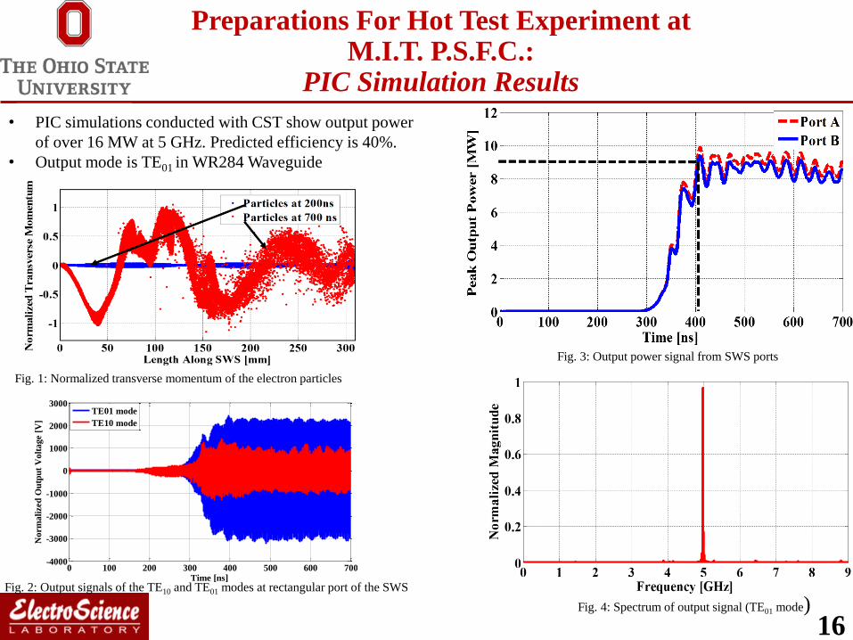
Preparations For Hot Test Experiment at M.I.T. P.S.F.C.:
PIC Simulation Results
• PIC simulations conducted with CST show output power
of over 16 MW at 5 GHz. Predicted efficiency is 40%.
• Output mode is TE01 in WR284 Waveguide
0 100 200 300 400 500 600 700-4000
-3000
-2000
-1000
0
1000
2000
3000
Time [ns]
Norm
ali
zed
Ou
tpu
t V
olt
age [
V]
TE01 mode
TE10 mode
Fig. 2: Output signals of the TE10 and TE01 modes at rectangular port of the SWS
Fig. 1: Normalized transverse momentum of the electron particles
Fig. 3: Output power signal from SWS ports
Fig. 4: Spectrum of output signal (TE01 mode)16

Preparations For Hot Test Experiment at M.I.T. P.S.F.C.:
Side Coupling and Propagation of TE01 mode
4.6 4.7 4.8 4.9 5 5.1 5.2 5.3 5.4 5.5 5.6-110
-100
-90
-80
-70
-60
-50
-40
Frequency [GHz]
S2
1 [
dB
] C
ou
pli
ng
fro
m T
E0
1 M
od
e
TE01 to TE10
TE01 to TE20
TE01 to TE01
4.5 4.6 4.7 4.8 4.9 5 5.1 5.2 5.3 5.4 5.5-3.5
-3
-2.5
-2
-1.5
-1
-0.5
0
Frequency [GHz]
S2
1 [
dB
]
TE01 mode
Fig. 2: S21 [dB] of TE01 mode propagating in WR284
waveguide with two 90 degree bends at 5GHz.
Fig. 1: Propagation of TE01 mode along 2 waveguide bends in a
WR284 waveguide.
Fig. 3: Proposed narrow wall hole coupling in WR284 waveguide
technique used to measure the output power from a TE01 mode at 5GHz.
Fig. 4: Coupling of TE10, TE20 and TE01 modes to the measurement
waveguide when the starting mode at the input port is TE0117

Preparations For Hot Test Experiment at M.I.T. P.S.F.C.:
Modal Power Content Analysis with CST
Mode Output power carried by
mode [MW]
Coupling factor at 5 GHz [dB]
(calculated by MIT)
TE10 2 -180
TE20 0.49 -180
TE01 8 -51
TE11 0.016 -52
TM11 0.25 -45
Fig. 1: Simulated geometry of SWS with output waveguides and the electric field intensity.
Table 1: Output power carried by first 5 modes and corresponding coupling factors at 5GHz
18

Preparations For Hot Test Experiment at M.I.T. P.S.F.C.:
Summary
19

Preparations For Hot Test Experiment at M.I.T. P.S.F.C.:
Future Work
• Resolve output power differences between full SWS with output and SWS
without output waveguides
• Develop CAD drawings for proposed SWS design.
• Fabrication of full SWS, mode converter and output coupler.
• Cold testing of SWS and output coupling system.
• Fabrication and cold testing of a TE01-mode based measurement system.
• SWS excitation and power measurements.
Hot Test Experiment
Novel Concepts for BWO SWSs
• Multi-section, inhomogeneous SWS study.
• Fabrication and cold testing of inhomogeneous SWSs.
• Exploitation of higher order dispersion for efficiency enhancement in BWOs.
• High frequency (W band SWS) design.
• Efficiency enhancements for W band BWOs.
• SWS fabrication and cold testing.
20