Hitachi HD61203 Controller Datasheet - Crystalfontz
30
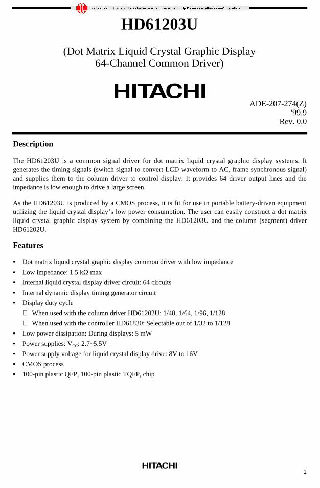
1 HD61203U (Dot Matrix Liquid Crystal Graphic Display 64-Channel Common Driver) ADE-207-274(Z) '99.9 Rev. 0.0 Description The HD61203U is a common signal driver for dot matrix liquid crystal graphic display systems. It generates the timing signals (switch signal to convert LCD waveform to AC, frame synchronous signal) and supplies them to the column driver to control display. It provides 64 driver output lines and the impedance is low enough to drive a large screen. As the HD61203U is produced by a CMOS process, it is fit for use in portable battery-driven equipment utilizing the liquid crystal display’s low power consumption. The user can easily construct a dot matrix liquid crystal graphic display system by combining the HD61203U and the column (segment) driver HD61202U. Features • Dot matrix liquid crystal graphic display common driver with low impedance • Low impedance: 1.5 kΩ max • Internal liquid crystal display driver circuit: 64 circuits • Internal dynamic display timing generator circuit • Display duty cycle When used with the column driver HD61202U: 1/48, 1/64, 1/96, 1/128 When used with the controller HD61830: Selectable out of 1/32 to 1/128 • Low power dissipation: During displays: 5 mW • Power supplies: V CC : 2.7~5.5V • Power supply voltage for liquid crystal display drive: 8V to 16V • CMOS process • 100-pin plastic QFP, 100-pin plastic TQFP, chip
Transcript of Hitachi HD61203 Controller Datasheet - Crystalfontz
1
HD61203U
(Dot Matrix Liquid Crystal Graphic Display64-Channel Common Driver)
ADE-207-274(Z)'99.9
Rev. 0.0
Description
The HD61203U is a common signal driver for dot matrix liquid crystal graphic display systems. Itgenerates the timing signals (switch signal to convert LCD waveform to AC, frame synchronous signal)and supplies them to the column driver to control display. It provides 64 driver output lines and theimpedance is low enough to drive a large screen.
As the HD61203U is produced by a CMOS process, it is fit for use in portable battery-driven equipmentutilizing the liquid crystal display’s low power consumption. The user can easily construct a dot matrixliquid crystal graphic display system by combining the HD61203U and the column (segment) driverHD61202U.
Features
• Dot matrix liquid crystal graphic display common driver with low impedance
• Low impedance: 1.5 kΩ max
• Internal liquid crystal display driver circuit: 64 circuits
• Internal dynamic display timing generator circuit
• Display duty cycle
When used with the column driver HD61202U: 1/48, 1/64, 1/96, 1/128
When used with the controller HD61830: Selectable out of 1/32 to 1/128
• Low power dissipation: During displays: 5 mW
• Power supplies: VCC: 2.7~5.5V
• Power supply voltage for liquid crystal display drive: 8V to 16V
• CMOS process
• 100-pin plastic QFP, 100-pin plastic TQFP, chip
HD61203U
2
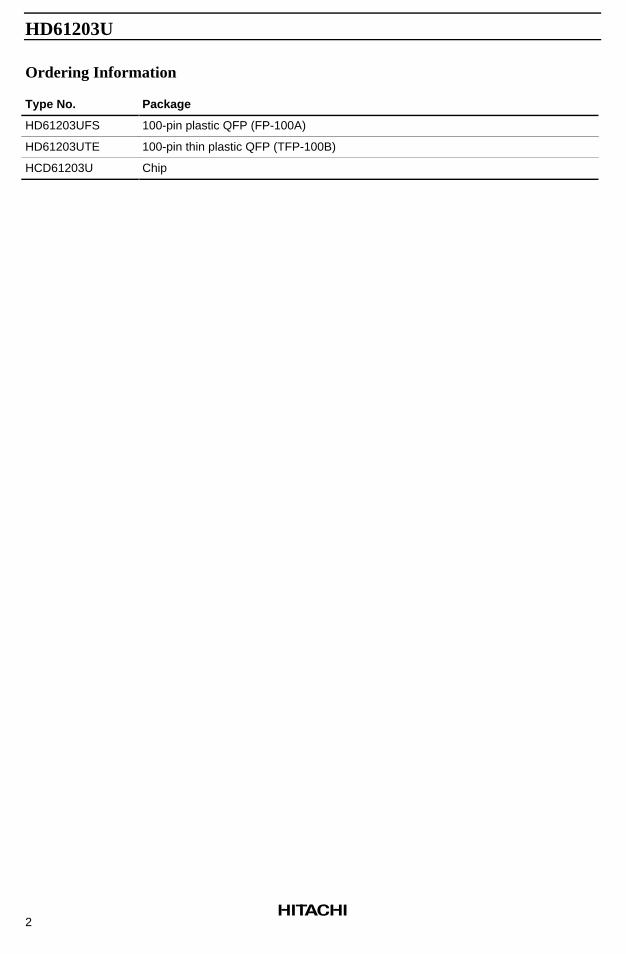
Ordering Information
Type No. Package
HD61203UFS 100-pin plastic QFP (FP-100A)
HD61203UTE 100-pin thin plastic QFP (TFP-100B)
HCD61203U Chip
HD61203U
3
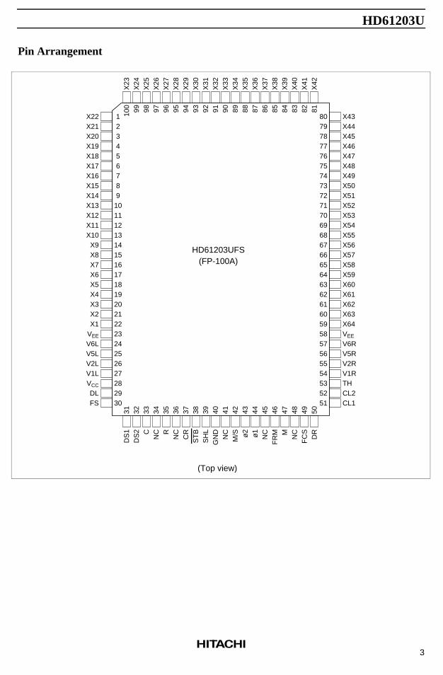
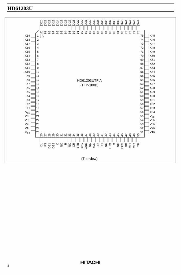
Pin Arrangement
807978777675747372717069686766656463626160595857565554535251
123456789
101112131415161718192021222324252627282930
100 99 98 97 96 95 94 93 92 91 90 89 88 87 86 85 84 83 82 81
31 32 33 34 35 36 37 38 39 40 41 42 43 44 45 46 47 48 49 50
X43X44X45X46X47X48X49X50X51X52X53X54X55X56X57X58X59X60X61X62X63X64VEE
V6RV5RV2RV1RTHCL2CL1
X23
X24
X25
X26
X27
X28
X29
X30
X31
X32
X33
X34
X35
X36
X37
X38
X39
X40
X41
X42
X22X21X20X19X18X17X16X15X14X13X12X11X10X9X8X7X6X5X4X3X2X1
VEE
V6LV5LV2LV1LVCC
DLFS
DS
1D
S2 C
NC R
NC
CR
ST
BS
HL
GN
DN
CM
/S ø2
ø1
NC
FR
M MN
CF
CS
DR
(Top view)
HD61203UFS(FP-100A)
HD61203U
4
75747372717069686766656463626160595857565554535251
123456789
10111213141516171819202122232425
100
99 98 97 96 95 94 93 92 91 90 89 88 87 86 85 84 83 82 81 80 79 78 77 76
26 27 28 29 30 31 32 33 34 35 36 37 38 39 40 41 42 43 44 45 46 47 48 49 50
X45X46X47X48X49X50X51X52X53X54X55X56X57X58X59X60X61X62X63X64VEE
V6RV5RV2RV1R
X20
X21
X22
X23
X24
X25
X26
X27
X28
X29
X30
X31
X32
X33
X34
X35
X36
X37
X38
X39
X40
X41
X42
X43
X44
X19X18X17X16X15X14X13X12X11X10
X9X8X7X6X5X4X3X2X1
VEE
V6LV5LV2LV1LVCC
DL
FS
DS
1D
S2 C
NC R
NC
CR
ST
BS
HL
GN
DN
CM
/S ø2
ø1
NC
FR
M MN
CF
CS
DR
CL1
CL2 TH
(Top view)
HD61203UTFIA(TFP-100B)
HD61203U
5
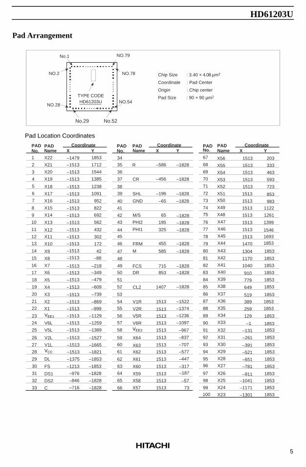
Pad Arrangement
Chip Size : 3.40 × 4.08 µm2
Coordinate : Pad Center
Origin : Chip center
Pad Size : 90 × 90 µm2
No.1
No.29
NO.28
TYPE CODEHD61203U
NO.2
No.52
NO.79
NO.54
NO.78
PADName
CoordinateX Y
CoordinateX Y
CoordinateX Y
PADName
PADName
2
3
4
5
6
7
8
9
10
11
12
13
14
15
16
17
18
19
20
21
22
23
24
25
50
49
48
47
46
45
44
43
42
41
40
39
38
37
36
35
34
33
32
31
30
29
28
27
26
51
52
53
54
55
56
57
58
59
60
76
77
78
79
80
81
82
83
84
85
61
62
63
64
65
66
67
68
69
70
86
87
88
89
90
91
92
93
94
95
71
72
73
74
75
96
97
98
99
100
1
X21
X20
X19
X18
X17
X16
X15
X14
X50
X49
X48
X47
X22
X23
X24
X25
X26
X27
X28
X29
X30
X31
X32
X33
X34
X35
X36
X37
X38
X39
X40
X41
X42
X43
X44
X45
X46
–1513 1712
1544
1385
1238
1091
952
822
692
562
432
302
172
42
–88
–218–349
–479
–609
–739
–869
–999
–1129
–1259
–1389
–1527
–1665
–1821
–1853
–1853
–1828
–1213
–976
–846
–716
–586
–456
–196
–65
65
195
325
455
585
715853
1407 –1828
–1522
–1374
–1236
–1097
–967
–837
–707
–577
–447
–317–187
–57
73
203
333
463
593
723
853
983
1122
1261
1399
1513
1513
1513
1513
1513 154616931853
1853
1470
1304
1170
1040
910
779
649
519
–1
–131
–261
–391
–521
–651
–781
–911–1041
–1171
–1301
–1479
1513
1853
1853
1853
1853
1853
1853
18531853
1853
1853
1853
1853
1853
1853
1853
1853
1853
1853
1513
1513
1513
1513
1513
1513
1513
1513
1513
1513
1513
1513
1513
1513
1513
1513
1513
1513
1513
–1513
–1513
–1375
–1828
–1828
–1828
–1828
–1828
–1828
–1828
–1828
–1828
–1828
–1828
–1828–1828
–1513
–1513
–1513
–1513
–1513
–1513
–1513
–1513
–1513
–1513
–1513
–1513
–1513
–1513
–1513
–1513
–1513
–1513
–1513
–1513
–1513
–1513
–1513
–1513
PADNo.
PADNo.
PADNo.
X13
X12
X11
X10
X9
X8
X7
X6
X5
X4
X3
X2
X1
V6L
V5L
V2L
V1L
DL
FS
DS1
DS2
C
R
CR
SHL
GND
M/S
PHI2
PHI1
FRM
M
FCSDR
CL2
V1R
V2R
V5R
V6R
X64
X63X62
X61
X60
X59
X58
X57
X56
X55
X54
X53
X52
X51
389
259
129
1853
1853
1853VEE1
VCC
VEE2
Pad Location Coordinates
HD61203U
6
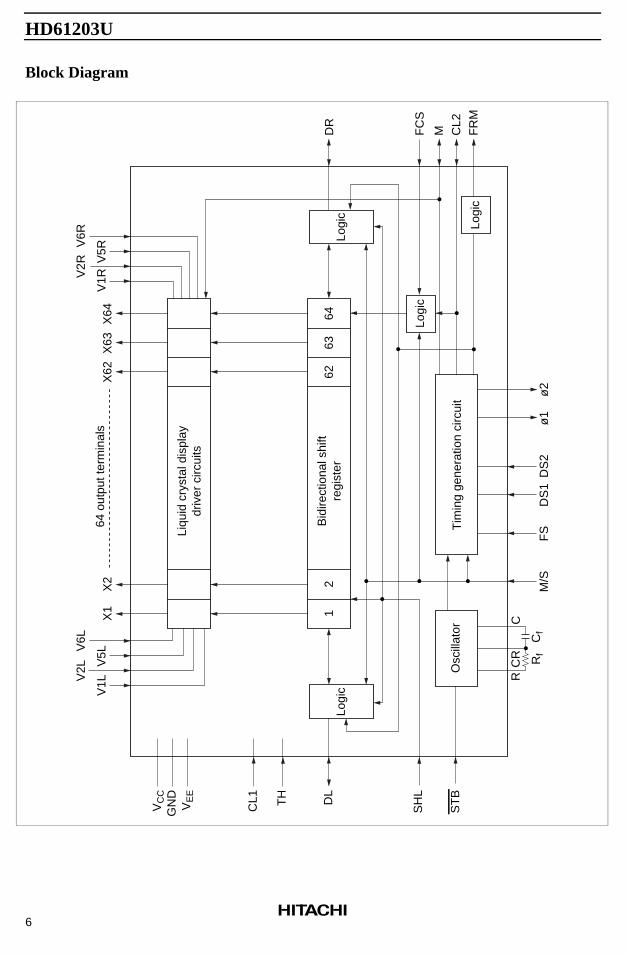
Block Diagram
Logi
cLo
gic
Logi
c
Logi
c
6463
621
2
64 o
utpu
t ter
min
als
Liqu
id c
ryst
al d
ispl
aydr
iver
circ
uits
Bid
irect
iona
l shi
ftre
gist
er
Tim
ing
gene
ratio
n ci
rcui
tO
scill
ator
DR
FC
S
M CL2
FR
M
VC
CG
ND
VE
E
CL1 TH DL
SH
L
ST
B
RC
R Rf
Cf
C
M/S
FS
DS
1D
S2
ø1
ø2
V1L
V5L
X1
X2
V2L
V6L
X62
X63
X64
V1RV
2R V5R
V6R
HD61203U
7
Block Functions
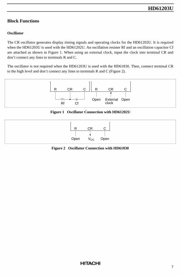
Oscillator
The CR oscillator generates display timing signals and operating clocks for the HD61202U. It is requiredwhen the HD61203U is used with the HD61202U. An oscillation resister Rf and an oscillation capacitor Cfare attached as shown in Figure 1. When using an external clock, input the clock into terminal CR anddon’t connect any lines to terminals R and C.
The oscillator is not required when the HD61203U is used with the HD61830. Then, connect terminal CRto the high level and don’t connect any lines to terminals R and C (Figure 2).
R CR C R CR C
Rf CfOpen OpenExternal
clock
Figure 1 Oscillator Connection with HD61202U
R CR C
Open OpenVCC
Figure 2 Oscillator Connection with HD61830
HD61203U
8
Timing Generator Circuit
The timing generator circuit generates display timing and operating clock for the HD61202U. This circuitis required when the HD61203U is used with the HD61202U. Connect terminal M/S to high level (mastermode). It is not necessary when the display timing signal is supplied from other circuits, for example, fromHD61830. In this case connect the terminals FS, DS1, and DS2 to high level and M/S to low level (slavemode).
Bidirectional Shift Register
A 64-bit bidirectional shift register. The data is shifted from DL to DR when SHL is at high level and fromDR to DL when SHL is at low level. In this case, CL2 is used as shift clock. The lowest order bit of thebidirectional shift register, which is on the DL side, corresponds to X1 and the highest order bit on the DRside corresponds to X64.
Liquid Crystal Display Driver Circuit
The combination of the data from the shift register with the M signal allows one of the four liquid crystaldisplay driver levels V1, V2, V5 and V6 to be transferred to the output terminals (Table 1).
Table 1 Output Levels
Data from the ShiftRegister M Output Level
1 1 V2
0 1 V6
1 0 V1
0 0 V5
HD61203U
9
HD61203U Terminal Functions
TerminalName
Number ofTerminals I/O Connected to Functions
VCC
GNDVEE
112
Power supply VCC–GND: Power supply for internal logic.
VCC–VEE: Power supply for driver circuit logic.
V1L, V2LV5L, V6LV1R, V2RV5R, V6R
8 Power supply Liquid crystal display driver level power supply.
V1L (V1R), V2L (V2R): Selected levelV5L (V5R), V6L (V6R): Non-selected level
Voltages of the level power supplies connectedto V1L and V1R should be the same. (Thisapplies to the combination of V2L & V2R, V5L &V5R and V6L & V6R respectively.)
M/S 1 I VCC or GND Selects master/slave.
• M/S = VCC: Master modeWhen the HD61203U is used with theHD61202U, timing generation circuitoperates to supply display timing signals andoperation clock to the HD61202U. Each ofI/O common terminals DL, DR, CL2, and Mis in the output state.
• M/S = GND: Slave modeThe timing operation circuit stops operating.The HD61203U is used in this mode whencombined with the HD61830. Even ifcombined with the HD61202U, this mode isused when display timing signals (M, data,CL2, etc.) are supplied by anotherHD61203U in the master mode. Terminals Mand CL2 are in the input state.
When SHL is VCC, DL is in the input state andDR is in the output state.
When SHL is GND, DL is in the output state andDR is in the input state.
FCS 1 I VCC or GND Selects shift clock phase.
• FCS = VCC
Shift register operates at the rising edge ofCL2. Select this condition when HD61203Uis used with HD61202U or when MA of theHD61830 connects to CL2 in combinationwith the HD61830.
• FCS = GNDShift register operates at the fall of CL2.Select this condition when CL1 of HD61830connects to CL2 in combination with theHD61830.
HD61203U
10
TerminalName
Number ofTerminals I/O Connected to Functions
FS 1 I VCC or GND Selects frequency.
When the frame frequency is 70 Hz, the oscillationfrequency should be:
fOSC = 430 kHz at FCS = VCC
fOSC = 215 kHz at FCS = GND
This terminal is active only in the master mode.Connect it to VCC in the slave mode.
DS1, DS2 2 I VCC or GND Selects display duty factor.
Display Duty Factor 1/48 1/64 1/96 1/128
DS1 GND GND VCC VCC
DS2 GND VCC GND VCC
These terminals are valid only in the master mode.Connect them to VCC in the slave mode.
STBTHCL1
111
I VCC or GND Input terminal for testing
Connect to STB VCC.Connect TH and CL1 to GND.
CR, R, C 3 Oscillator
In the master mode, use these terminals as shownbelow:
R CR C R CR C
Rf Cf Open OpenExternal
clock
Internal oscillation External clock
In the slave mode, stop the oscillator as shownbelow:
R CR C
Open OpenVCC
ø1, ø2 2 O HD61202U Operating clock output terminals for the HD61202U
• Master modeConnect these terminals to terminals ø1 and ø2of the HD61202U respectively.
• Slave modeDon’t connect any lines to these terminals.
HD61203U
11
TerminalName
Number ofTerminals I/O Connected to Functions
FRM 1 O HD61202U Frame signal
• Master modeConnect this terminal to terminal FRM of theHD61202U.
• Slave modeDon’t connect any lines to this terminal.
M 1 I/O MB ofHD61830 or Mof HD61202U
Signal to convert LCD driver signal into AC
• Master mode: Output terminalConnect this terminal to terminal M of theHD61202U.
• Slave mode: Input terminalConnect this terminal to terminal MB of theHD61830.
CL2 1 I/O CL1 or MA ofHD61830 orCL ofHD61202U
Shift clock
• Master mode: Output terminalConnect this terminal to terminal CL of theHD61202U.
• Slave mode: Input terminalConnect this terminal to terminal CL1 or MA ofthe HD61830.
DL, DR 2 I/O Open or FLMof HD61830
Data I/O terminals of bidirectional shift register
DL corresponds to X1’s side and DR to X64’s side.
• Master modeOutput common scanning signal. Don’t connectany lines to these terminals normally.
• Slave modeConnect terminal FLM of the HD61830 to DL(when SHL = VCC) or DR (when SHL = GND).
M/S VCC GND
SHL VCC GND VCC GND
DL Output Output Input Output
DR Output Output Output Input
NC 5 Open Not used.
Don’t connect any lines to this terminal.
SHL 1 I VCC or GND Selects shift direction of bidirectional shift register.
SHL Shift DirectionCommonScanning Direction
VCC DL → DR X1 → X64
GND DL ← DR X1 ← X64
HD61203U
12
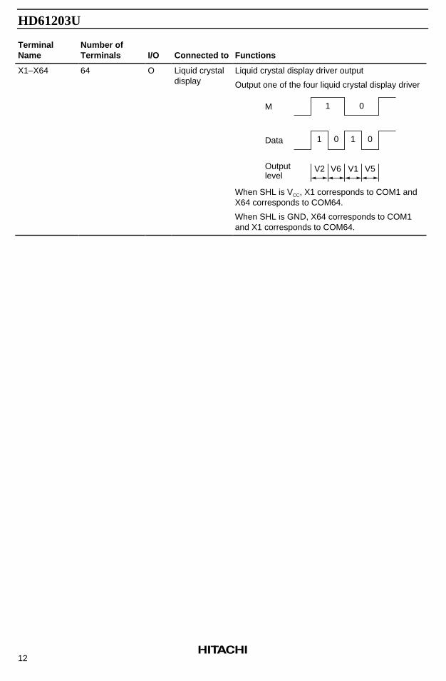
TerminalName
Number ofTerminals I/O Connected to Functions
X1–X64 64 O Liquid crystaldisplay
Liquid crystal display driver output
Output one of the four liquid crystal display driver
M
Data
Outputlevel
1 0
1 0 1 0
V2 V6 V1 V5
When SHL is VCC, X1 corresponds to COM1 andX64 corresponds to COM64.
When SHL is GND, X64 corresponds to COM1and X1 corresponds to COM64.
HD61203U
13
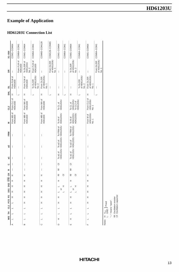
Example of Application
HD61203U Connection List
M/S
TH
CL
1F
CS
FS
DS
1D
S2
ST
BC
RR
Cø
1ø
2F
RM
MC
L2
SH
LD
LD
RX
1–X
64
AL
LL
LH
HH
HH
——
——
—Fr
om M
B o
fFr
om C
L1 o
fH
From
FLM
of
—C
OM
1–C
OM
64H
D61
830
HD
6183
0H
D61
830
L—
From
FLM
of
CO
M64
–CO
M1
HD
6183
0
BL
LL
HH
HH
HH
——
——
—Fr
om M
B o
fFr
om M
A o
fH
From
FLM
of
To D
L/D
R o
fC
OM
1–C
OM
64H
D61
830
HD
6183
0H
D61
830
HD
6120
3UN
o. 2
LTo
DL/
DR
From
FLM
of
CO
M64
–CO
M1
of H
D61
203U
HD
6183
0N
o. 2
CL
LL
HH
HH
HH
——
——
—Fr
om M
B o
fFr
om M
A o
fH
From
DL/
DR
—C
OM
65–C
OM
128
HD
6183
0H
D61
830
of H
D61
203U
No.
1
L—
From
DL/
DR
CO
M12
8–C
OM
65of
HD
6120
3UN
o. 1
DH
LL
HH
LL
HR
fR
fC
fTo
ø1
ofTo
ø2
ofTo
FR
M o
fTo
M o
fTo
CL
ofH
——
CO
M1–
CO
M64
orH
D61
202U
HD
6120
2UH
D61
202U
HD
6120
2UH
D61
202U
LH
Cf
L—
—C
OM
64–C
OM
1
EH
LL
HH
LL
HR
fR
fC
fTo
ø1
ofTo
ø2
ofTo
FR
M o
fTo
M o
fTo
CL
ofH
—To
DL/
DR
C
OM
1–C
OM
64or
HD
6120
2UH
D61
202U
HD
6120
2UH
D61
202U
HD
6120
2Uof
HD
6120
3UL
HC
fH
D61
203U
To C
L2 o
fN
o. 2
HD
6120
3UL
To D
L/D
R—
CO
M64
–CO
M1
of H
D61
203U
No.
2
FL
LL
HH
HH
HH
——
——
—Fr
om M
of
From
CL2
of
HFr
om D
L/D
R—
CO
M1–
CO
M64
HD
6120
3UH
D61
203U
of H
D61
203U
No.
1N
o. 1
No.
1
L—
From
DL/
DR
C
OM
64–C
OM
1of
HD
6120
3UN
o. 1
Not
es:
H:
VC
CF
ixed
L:G
ND
“—”
mea
ns “
open
”.
Rf:
Osc
illat
ion
resi
ster
Cf:
Osc
illat
ion
capa
cito
r
HD61203U
14
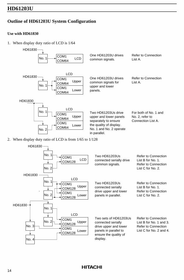
Outline of HD61203U System Configuration
Use with HD61830
1. When display duty ratio of LCD is 1/64
No. 1COM1COM64
LCD
No. 1
HD61830
HD61830LCD
No. 1
HD61830
No. 2
COM1COM64
COM1COM64
Upper
Lower
COM1COM64
COM1COM64
Lower
Upper
LCD
One HD61203U drivescommon signals.
Refer to Connection List A.
One HD61203U drives common signals for upper and lower panels.
Refer to Connection List A.
Two HD61203Us driveupper and lower panelsseparately to ensure the quality of display.No. 1 and No. 2 operatein parallel.
For both of No. 1 andNo. 2, refer to Connection List A.
2. When display duty ratio of LCD is from 1/65 to 1/128
No. 1COM1COM128
LCD
HD61830
No. 2
No. 1
HD61830
COM1COM128
COM1COM128
Upper
Lower
LCD
No. 2
COM1COM128
COM1COM128
Upper
Lower
LCD
No. 1
No. 2No. 3
No. 4
HD61830
Two HD61203Us connected serially drivecommon signals.
Refer to ConnectionList B for No. 1.Refer to Connection List C for No. 2.
Two HD61203Usconnected seriallydrive upper and lowerpanels in parallel.
Refer to Connection List B for No. 1.Refer to ConnectionList C for No. 2.
Two sets of HD61203Usconnected serially drive upper and lowerpanels in parallel toensure the quality ofdisplay.
Refer to ConnectionList B for No. 1 and 3.Refer to ConnectionList C for No. 2 and 4.
HD61203U
15
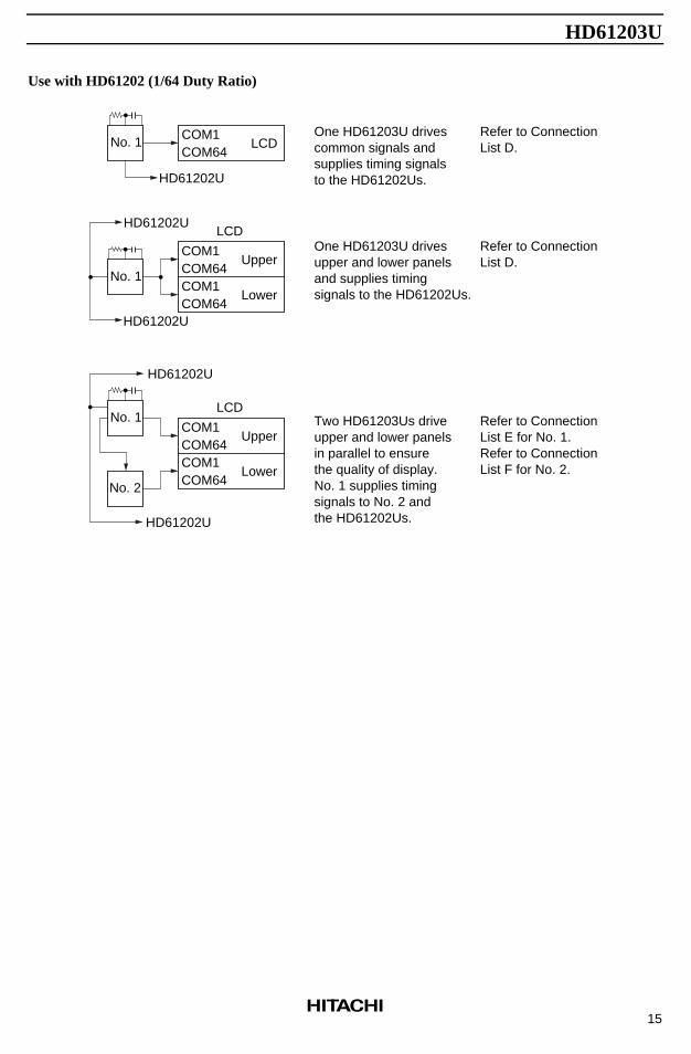
Use with HD61202 (1/64 Duty Ratio)
No. 1COM1COM64
LCD
HD61202U
LCD
COM1COM64
COM1COM64
Upper
Lower
COM1COM64
COM1COM64
Lower
Upper
LCD
One HD61203U drivescommon signals andsupplies timing signalsto the HD61202Us.
Refer to ConnectionList D.
One HD61203U drives upper and lower panelsand supplies timingsignals to the HD61202Us.
Refer to ConnectionList D.
Two HD61203Us driveupper and lower panelsin parallel to ensurethe quality of display.No. 1 supplies timingsignals to No. 2 and the HD61202Us.
Refer to ConnectionList E for No. 1.Refer to ConnectionList F for No. 2.
No. 1
HD61202U
HD61202U
No. 1
HD61202U
HD61202U
No. 2
HD61203U
16
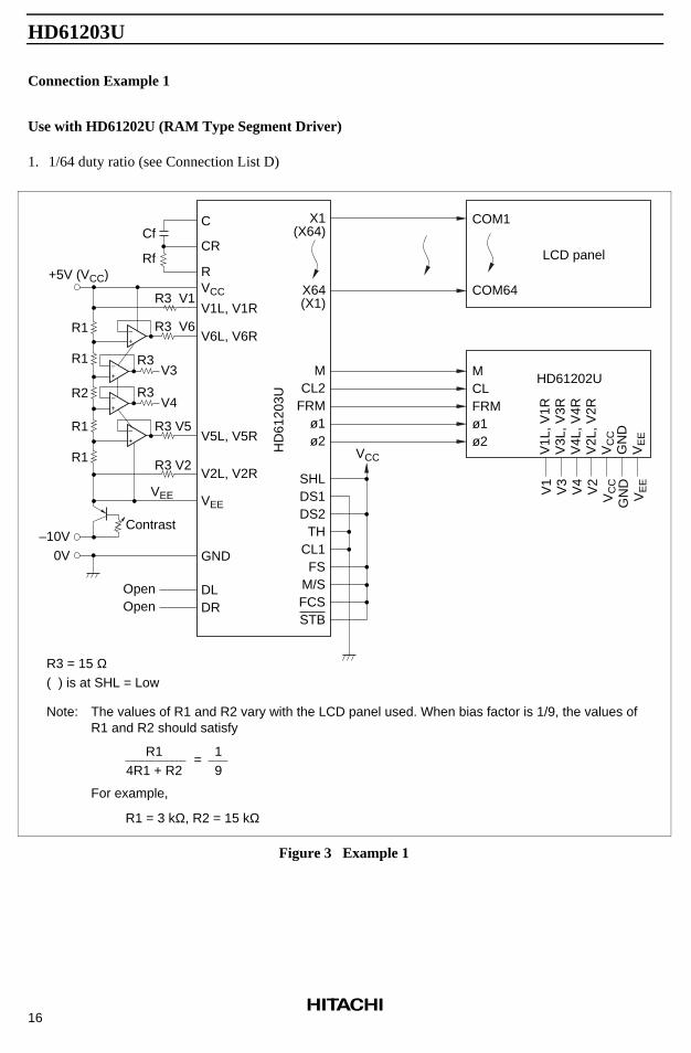
Connection Example 1
Use with HD61202U (RAM Type Segment Driver)
1. 1/64 duty ratio (see Connection List D)
–+
–+
R3 V1
R3 V6
R3V3
R3V4
R3 V5
R3 V2
VEE
Contrast
OpenOpen
VCC
–+
–+
+5V (VCC)
R1
R1
R2
R1
R1
–10V
0V
X1(X64)
MCL2
FRMø1ø2
X64(X1)
SHLDS1DS2
THCL1FS
M/SFCSSTB
C
CR
R
Cf
Rf
VCC
V1L, V1R
V6L, V6R
V5L, V5R
V2L, V2R
VEE
GND
DLDR
R3 = 15 Ω( ) is at SHL = Low
COM1
COM64
LCD panel
HD
6120
3U
MCLFRMø1ø2
HD61202U
V1L
, V1R
V3L
, V3R
V4L
, V4R
V2L
, V2R
VC
CG
ND
VE
E
V1
V3
V4
V2
VC
CG
ND
VE
E
Note: The values of R1 and R2 vary with the LCD panel used. When bias factor is 1/9, the values of R1 and R2 should satisfy
R14R1 + R2
=19
For example,
R1 = 3 kΩ, R2 = 15 kΩ
Figure 3 Example 1
HD61203U
17
ø2
CL2
DL
(DR
)
C ø1
ø2
CL2
FR
M
DL
(DR
)
DR
(DL)
M X1
(X64
)
X2
(X63
)
12
363
641
23
6364
1
**
**
**
1 fr
ame
1 fr
ame
V6
V6
V5
V1
V1
V5
V5
V2
V6
V6
V2
V6
V5
V1
12
3
4748
49
( )
: at S
HL
= L
owN
ote:
*
Pha
se d
iffer
ence
bet
wee
n D
L (D
R)
and
CL2
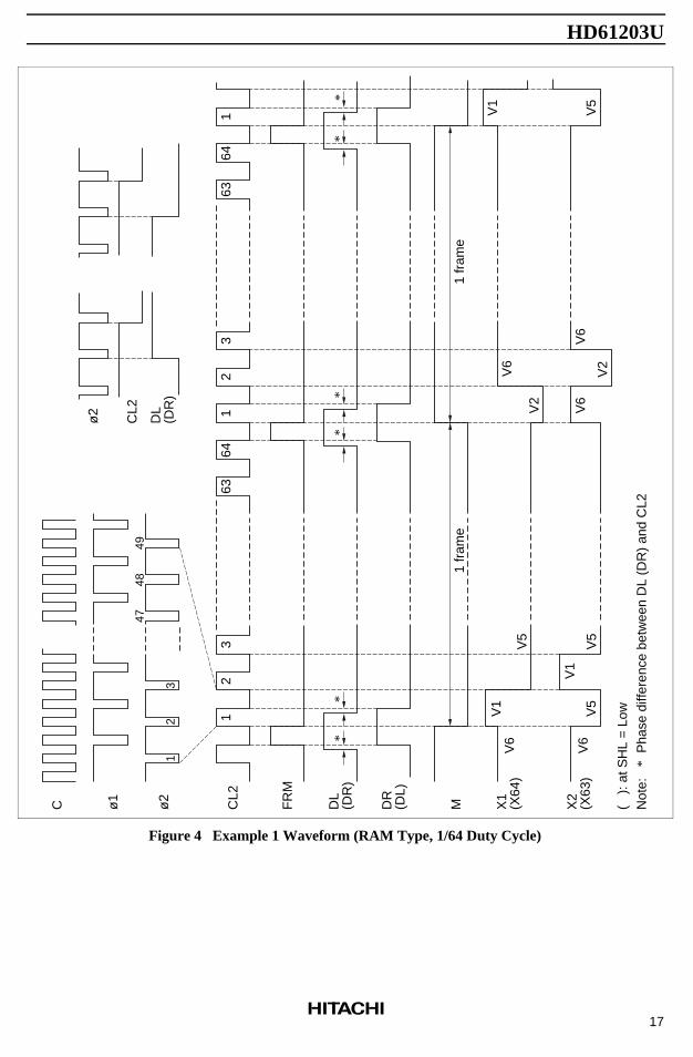
Figure 4 Example 1 Waveform (RAM Type, 1/64 Duty Cycle)
HD61203U
18
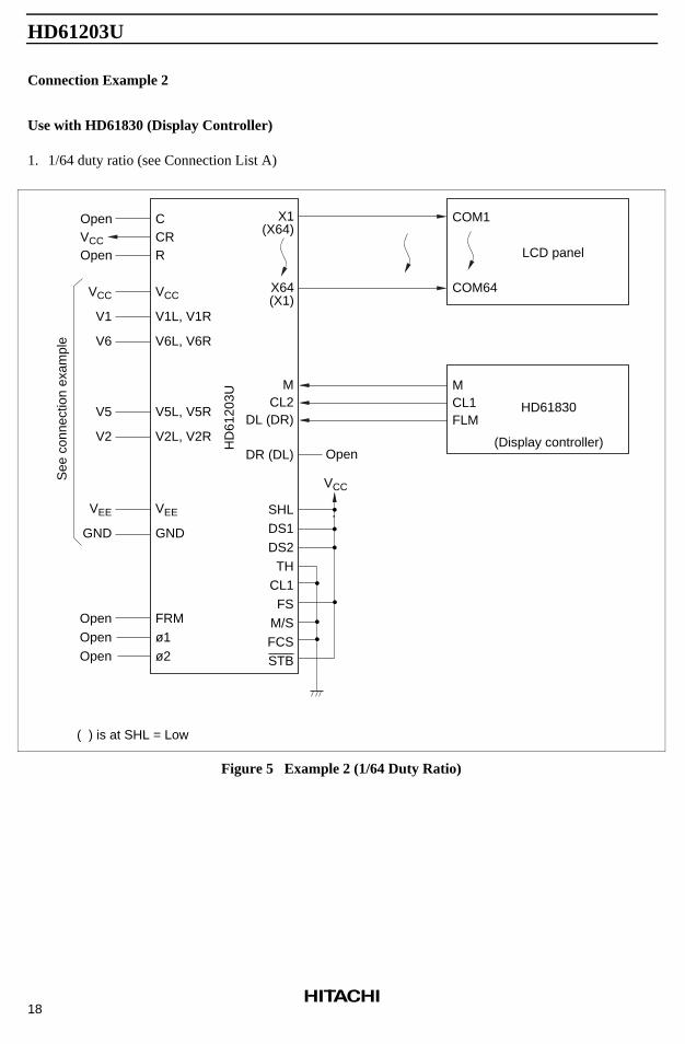
Connection Example 2
Use with HD61830 (Display Controller)
1. 1/64 duty ratio (see Connection List A)
OpenVCC
Open
VCC
V1
V6
V5
V2
VEE
GND
OpenOpenOpen
See
con
nect
ion
exam
ple
VCC
Open
X1(X64)
MCL2
DL (DR)
DR (DL)
X64(X1)
SHLDS1DS2
THCL1FS
M/SFCSSTB
COM1
COM64
LCD panel
HD
6120
3U
MCL1FLM
HD61830
(Display controller)
CCRR
VCC
V1L, V1R
V6L, V6R
V5L, V5R
V2L, V2R
VEE
GND
FRMø1ø2
( ) is at SHL = Low
Figure 5 Example 2 (1/64 Duty Ratio)
HD61203U
19
1 fr
ame
1 fr
ame
12
34
641
23
641
V6
V1
V5
V1
V6
V5
V5
V6
V6
V2
V6
V2
V1
V5
V5
V2
V6
V1
V5
V2
( )
: at S
HL
= L
ow
MB
FLM
CL1 X
1(X
64)
X2
(X63
)
X64
(X1)
V6
From HD61830
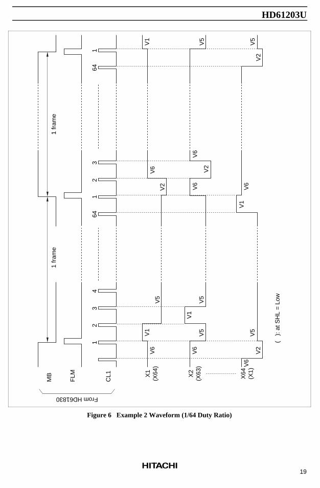
Figure 6 Example 2 Waveform (1/64 Duty Ratio)
HD61203U
20
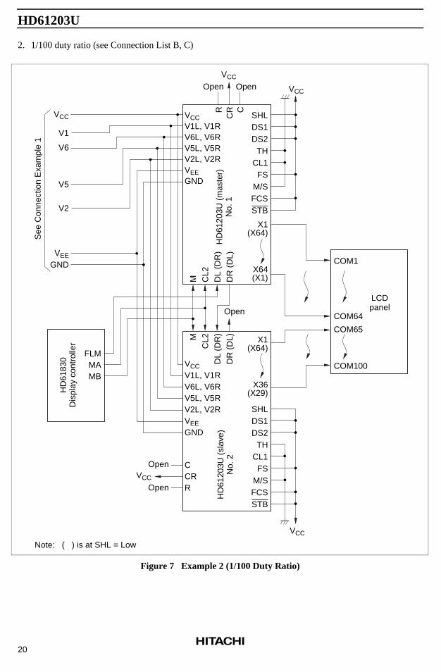
2. 1/100 duty ratio (see Connection List B, C)
VCC
VCC
COM1
COM64
COM65
COM100
LCDpanel
SHLDS1DS2
THCL1FS
M/SFCSSTB
X1(X64)
X64(X1)
X1(X64)
X36(X29)
SHLDS1DS2
THCL1FS
M/SFCSSTB
VCCV1L, V1RV6L, V6RV5L, V5RV2L, V2RVEEGND
VCC
OpenOpen
RC
R C
M CL2
DL
(DR
)D
R (
DL)
HD
6120
3U (
mas
ter)
No.
1
MC
L2D
L (D
R)
DR
(D
L)
Open
HD
6120
3U (
slav
e)N
o. 2
VCC
V1L, V1RV6L, V6RV5L, V5RV2L, V2RVEE
GND
CCRR
Open
Open
VCC
FLMMAMB
HD
6183
0D
ispl
ay c
ontr
olle
r
See
Con
nect
ion
Exa
mpl
e 1
VCC
V1
V6
V5
V2
VEE
GND
Note: ( ) is at SHL = Low
Figure 7 Example 2 (1/100 Duty Ratio)
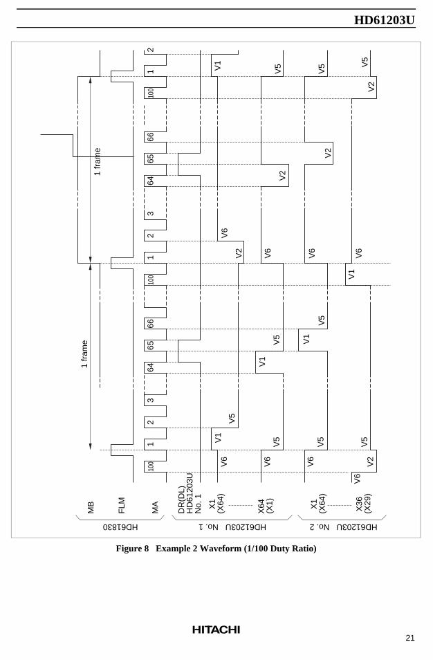
HD61203U
21
1 fr
ame
1 fr
ame
12
100
364
6566
100
12
364
6566
100
12
V6
V1
V5
V6
V6
V2
V5
V5
V5
V6
V1
V5
V1
V5
V1
V6
V6
V6
V2
V6
V2
V2
V1
V5
V5 V
5V
2
MB
FLM
MA
DR
(DL)
HD
6120
3UN
o. 1
X1
(X64
)
X64
(X1)
X1
(X64
)
X36
(X29
)
HD61830 HD61203U No. 1 HD61203U No. 2
Figure 8 Example 2 Waveform (1/100 Duty Ratio)
HD61203U
22
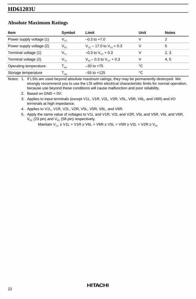
Absolute Maximum Ratings
Item Symbol Limit Unit Notes
Power supply voltage (1) VCC –0.3 to +7.0 V 2
Power supply voltage (2) VEE VCC – 17.0 to VCC + 0.3 V 5
Terminal voltage (1) VT1 –0.3 to VCC + 0.3 V 2, 3
Terminal voltage (2) VT2 VEE – 0.3 to VCC + 0.3 V 4, 5
Operating temperature Topr –30 to +75 °C
Storage temperature Tstg –55 to +125 °C
Notes: 1. If LSIs are used beyond absolute maximum ratings, they may be permanently destroyed. Westrongly recommend you to use the LSI within electrical characteristic limits for normal operation,because use beyond these conditions will cause malfunction and poor reliability.
2. Based on GND = 0V.3. Applies to input terminals (except V1L, V1R, V2L, V2R, V5L, V5R, V6L, and V6R) and I/O
terminals at high impedance.4. Applies to V1L, V1R, V2L, V2R, V5L, V5R, V6L, and V6R.5. Apply the same value of voltages to V1L and V1R, V2L and V2R, V5L and V5R, V6L and V6R,
VEE (23 pin) and VEE (58 pin) respectively.Maintain VCC ≥ V1L = V1R ≥ V6L = V6R ≥ V5L = V5R ≥ V2L = V2R ≥ VEE
HD61203U
23
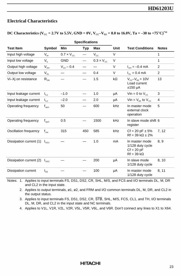
Electrical Characteristics
DC Characteristics (VCC = 2.7V to 5.5V, GND = 0V, VCC–VEE = 8.0 to 16.0V, Ta = –30 to +75°C)*14
Specifications
Test Item Symbol Min Typ Max Unit Test Conditions Notes
Input high voltage VIH 0.7 × VCC — VCC V 1
Input low voltage VIL GND — 0.3 × VCC V 1
Output high voltage VOH VCC – 0.4 — — V IOH = –0.4 mA 2
Output low voltage VOL — — 0.4 V IOL = 0.4 mA 2
Vi–Xj on resistance RON — — 1.5 kΩ VCC–VEE = 10VLoad current±150 µA
13
Input leakage current IIL1 –1.0 — 1.0 µA Vin = 0 to VCC 3
Input leakage current IIL2 –2.0 — 2.0 µA Vin = VEE to VCC 4
Operating frequency fopr1 50 — 600 kHz In master modeexternal clockoperation
5
Operating frequency fopr2 0.5 — 1500 kHz In slave mode shiftregister
6
Oscillation frequency fosc 315 450 585 kHz Cf = 20 pF ± 5%Rf = 39 kΩ ± 2%
7, 12
Dissipation current (1) IGG1 — — 1.0 mA In master mode1/128 duty cycleCf = 20 pFRf = 39 kΩ
8, 9
Dissipation current (2) IGG2 — — 200 µA In slave mode1/128 duty cycle
8, 10
Dissipation current IEE — — 100 µA In master mode1/128 duty cycle
8, 11
Notes: 1. Applies to input terminals FS, DS1, DS2, CR, SHL, M/S, and FCS and I/O terminals DL, M, DRand CL2 in the input state.
2. Applies to output terminals, ø1, ø2, and FRM and I/O common terminals DL, M, DR, and CL2 inthe output status.
3. Applies to input terminals FS, DS1, DS2, CR, STB, SHL, M/S, FCS, CL1, and TH, I/O terminalsDL, M, DR, and CL2 in the input state and NC terminals.
4. Applies to V1L, V1R, V2L, V2R, V5L, V5R, V6L, and V6R. Don’t connect any lines to X1 to X64.
HD61203U
24
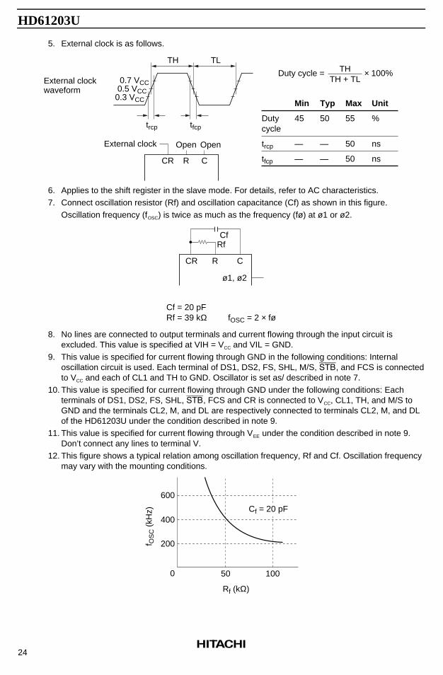
5. External clock is as follows.
TH TL
tfcptrcp
0.7 VCC 0.5 VCC0.3 VCC
Open Open
CR R C
External clock
External clockwaveform
Duty cycle
trcp
tfcp
Min
45
—
—
Typ
50
—
—
Max
55
50
50
Unit
%
ns
ns
Duty cycle = THTH + TL
× 100%
6. Applies to the shift register in the slave mode. For details, refer to AC characteristics.7. Connect oscillation resistor (Rf) and oscillation capacitance (Cf) as shown in this figure.
Oscillation frequency (fOSC) is twice as much as the frequency (fø) at ø1 or ø2.
CfRf
CR R C
ø1, ø2
Cf = 20 pFRf = 39 kΩ fOSC = 2 × fø
8. No lines are connected to output terminals and current flowing through the input circuit isexcluded. This value is specified at VIH = VCC and VIL = GND.
9. This value is specified for current flowing through GND in the following conditions: Internaloscillation circuit is used. Each terminal of DS1, DS2, FS, SHL, M/S, STB, and FCS is connectedto VCC and each of CL1 and TH to GND. Oscillator is set as/ described in note 7.
10. This value is specified for current flowing through GND under the following conditions: Eachterminals of DS1, DS2, FS, SHL, STB, FCS and CR is connected to VCC, CL1, TH, and M/S toGND and the terminals CL2, M, and DL are respectively connected to terminals CL2, M, and DLof the HD61203U under the condition described in note 9.
11. This value is specified for current flowing through VEE under the condition described in note 9.Don’t connect any lines to terminal V.
12. This figure shows a typical relation among oscillation frequency, Rf and Cf. Oscillation frequencymay vary with the mounting conditions.
Cf = 20 pF
50 100
Rf (kΩ)
600
400
200
0
f OS
C (
kHz)
HD61203U
25
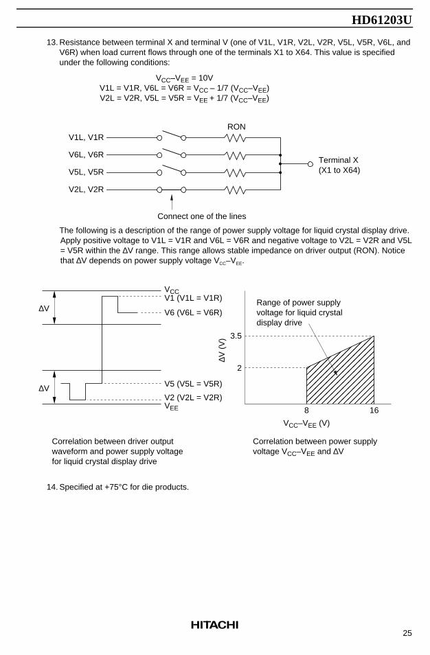
13. Resistance between terminal X and terminal V (one of V1L, V1R, V2L, V2R, V5L, V5R, V6L, andV6R) when load current flows through one of the terminals X1 to X64. This value is specifiedunder the following conditions:
Terminal X(X1 to X64)
V1L, V1R
V6L, V6R
V5L, V5R
V2L, V2R
RON
VCC–VEE = 10VV1L = V1R, V6L = V6R = VCC – 1/7 (VCC–VEE)V2L = V2R, V5L = V5R = VEE + 1/7 (VCC–VEE)
Connect one of the lines
The following is a description of the range of power supply voltage for liquid crystal display drive.Apply positive voltage to V1L = V1R and V6L = V6R and negative voltage to V2L = V2R and V5L= V5R within the ∆V range. This range allows stable impedance on driver output (RON). Noticethat ∆V depends on power supply voltage VCC–VEE.
∆V
∆V
VCCV1 (V1L = V1R)
V6 (V6L = V6R)
V5 (V5L = V5R)
V2 (V2L = V2R)VEE
3.5
2
∆V (
V)
8 16
VCC–VEE (V)
Range of power supplyvoltage for liquid crystaldisplay drive
Correlation between driver outputwaveform and power supply voltagefor liquid crystal display drive
Correlation between power supplyvoltage VCC–VEE and ∆V
14. Specified at +75°C for die products.
HD61203U
26
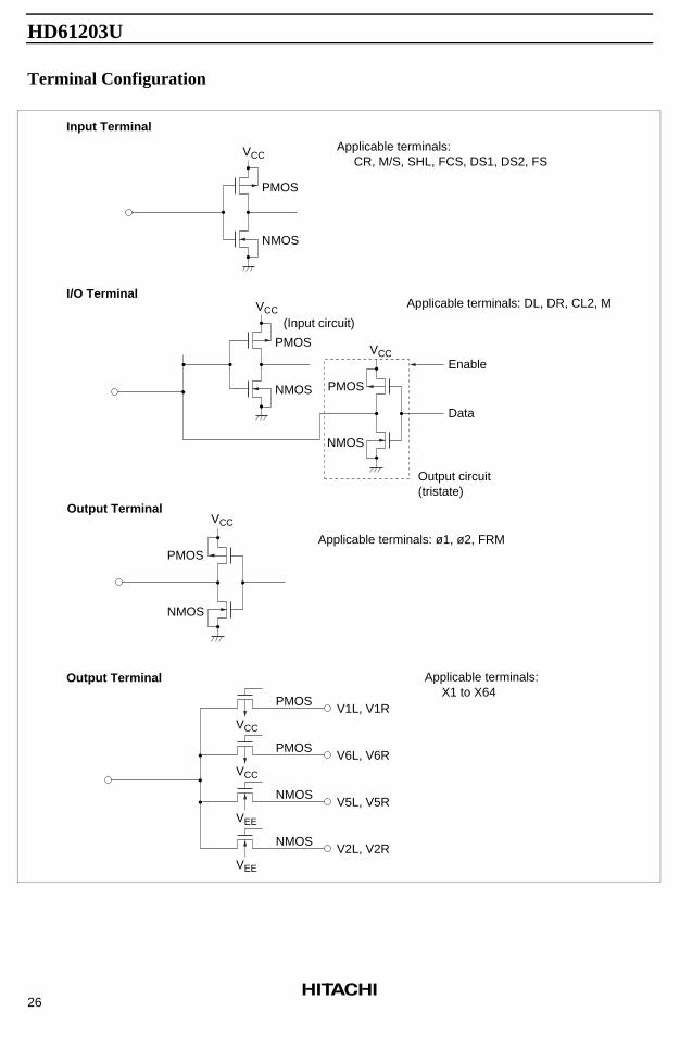
Terminal Configuration
PMOS
VCC
NMOS
Applicable terminals: CR, M/S, SHL, FCS, DS1, DS2, FS
Applicable terminals: DL, DR, CL2, MI/O Terminal
Input Terminal
PMOS
NMOS
VCC
Output Terminal
VCC
PMOSV1L, V1R
VCC
PMOSV6L, V6R
VEE
NMOSV5L, V5R
VEE
NMOSV2L, V2R
Applicable terminals: X1 to X64
PMOS
VCC
NMOS
(Input circuit)
Enable
Data
Output circuit(tristate)
Output Terminal
PMOS
NMOS
VCC
Applicable terminals: ø1, ø2, FRM
HD61203U
27
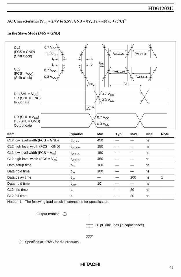
AC Characteristics (VCC = 2.7V to 5.5V, GND = 0V, Ta = –30 to +75°C)*2
In the Slave Mode (M/S = GND)
0.7 VCC
0.3 VCC
tftr
trtf
tDS
tDH
tWLCL2L
tWHCL2H
tWLCL2H
tWHCL2L
0.7 VCC
0.3 VCC
0.7 VCC
0.3 VCC
tDD
tDHW
0.7 VCC
0.3 VCC
CL2(FCS = GND)(Shift clock)
CL2(FCS = VCC)(Shift clock)
DL (SHL = VCC)DR (SHL = GND)Input data
DR (SHL = VCC)DL (SHL = GND)Output data
Item Symbol Min Typ Max Unit Note
CL2 low level width (FCS = GND) tWLCL2L 450 — — ns
CL2 high level width (FCS = GND) tWLCL2H 150 — — ns
CL2 low level width (FCS = VCC) tWHCL2L 150 — — ns
CL2 high level width (FCS = VCC) tWHCL2H 450 — — ns
Data setup time tDS 100 — — ns
Data hold time tDH 100 — — ns
Data delay time tDD — — 200 ns 1
Data hold time tDHW 10 — — ns
CL2 rise time tr — — 30 ns
CL2 fall time tf — — 30 ns
Notes: 1. The following load circuit is connected for specification.
30 pF (includes jig capacitance)
Output terminal
2. Specified at +75°C for die products.
HD61203U
28
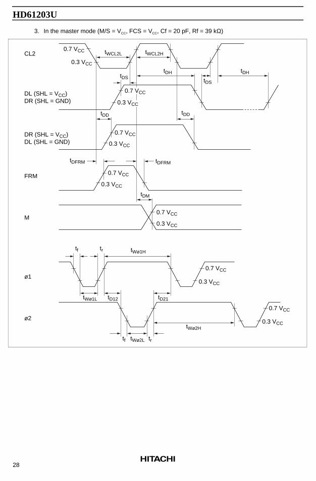
3. In the master mode (M/S = VCC, FCS = VCC, Cf = 20 pF, Rf = 39 kΩ)
0.7 VCC
0.3 VCC
tWCL2L tWCL2H
tDH
tDS
tDH
tDD
tDS
0.7 VCC
0.3 VCC
tDD
0.7 VCC
0.3 VCC
0.3 VCC
0.7 VCC
tDFRMtDFRM
tDM
0.7 VCC
0.3 VCC
tWø1Htrtf
tWø2Ltf tr
tWø2H
tD21tD12tWø1L
0.7 VCC 0.3 VCC
0.7 VCC 0.3 VCC
CL2
DL (SHL = VCC)DR (SHL = GND)
DR (SHL = VCC)DL (SHL = GND)
FRM
M
ø1
ø2
HD61203U
29
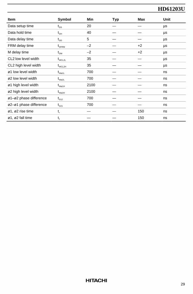
Item Symbol Min Typ Max Unit
Data setup time tDS 20 — — µs
Data hold time tDH 40 — — µs
Data delay time tDD 5 — — µs
FRM delay time tDFRM –2 — +2 µs
M delay time tDM –2 — +2 µs
CL2 low level width tWCL2L 35 — — µs
CL2 high level width tWCL2H 35 — — µs
ø1 low level width tWø1L 700 — — ns
ø2 low level width tWø2L 700 — — ns
ø1 high level width tWø1H 2100 — — ns
ø2 high level width tWø2H 2100 — — ns
ø1–ø2 phase difference tD12 700 — — ns
ø2–ø1 phase difference tD21 700 — — ns
ø1, ø2 rise time tr — — 150 ns
ø1, ø2 fall time tf — — 150 ns
HD61203U
30
Cautions
1. Hitachi neither warrants nor grants licenses of any rights of Hitachi’s or any third party’s patent,copyright, trademark, or other intellectual property rights for information contained in this document.Hitachi bears no responsibility for problems that may arise with third party’s rights, includingintellectual property rights, in connection with use of the information contained in this document.
2. Products and product specifications may be subject to change without notice. Confirm that you havereceived the latest product standards or specifications before final design, purchase or use.
3. Hitachi makes every attempt to ensure that its products are of high quality and reliability. However,contact Hitachi’s sales office before using the product in an application that demands especially highquality and reliability or where its failure or malfunction may directly threaten human life or cause riskof bodily injury, such as aerospace, aeronautics, nuclear power, combustion control, transportation,traffic, safety equipment or medical equipment for life support.
4. Design your application so that the product is used within the ranges guaranteed by Hitachi particularlyfor maximum rating, operating supply voltage range, heat radiation characteristics, installationconditions and other characteristics. Hitachi bears no responsibility for failure or damage when usedbeyond the guaranteed ranges. Even within the guaranteed ranges, consider normally foreseeablefailure rates or failure modes in semiconductor devices and employ systemic measures such as fail-safes, so that the equipment incorporating Hitachi product does not cause bodily injury, fire or otherconsequential damage due to operation of the Hitachi product.
5. This product is not designed to be radiation resistant.
6. No one is permitted to reproduce or duplicate, in any form, the whole or part of this document withoutwritten approval from Hitachi.
7. Contact Hitachi’s sales office for any questions regarding this document or Hitachi semiconductorproducts.
Hitachi, Ltd.Semiconductor & Integrated Circuits.Nippon Bldg., 2-6-2, Ohte-machi, Chiyoda-ku, Tokyo 100-0004, JapanTel: Tokyo (03) 3270-2111 Fax: (03) 3270-5109
Copyright © Hitachi, Ltd., 1998. All rights reserved. Printed in Japan.
Hitachi Asia Pte. Ltd.16 Collyer Quay #20-00Hitachi TowerSingapore 049318Tel: 535-2100Fax: 535-1533
URL NorthAmerica : http:semiconductor.hitachi.com/Europe : http://www.hitachi-eu.com/hel/ecgAsia (Singapore) : http://www.has.hitachi.com.sg/grp3/sicd/index.htmAsia (Taiwan) : http://www.hitachi.com.tw/E/Product/SICD_Frame.htmAsia (HongKong) : http://www.hitachi.com.hk/eng/bo/grp3/index.htmJapan : http://www.hitachi.co.jp/Sicd/indx.htm
Hitachi Asia Ltd.Taipei Branch Office3F, Hung Kuo Building. No.167, Tun-Hwa North Road, Taipei (105)Tel: <886> (2) 2718-3666Fax: <886> (2) 2718-8180
Hitachi Asia (Hong Kong) Ltd.Group III (Electronic Components)7/F., North Tower, World Finance Centre,Harbour City, Canton Road, Tsim Sha Tsui,Kowloon, Hong KongTel: <852> (2) 735 9218Fax: <852> (2) 730 0281 Telex: 40815 HITEC HXHitachi Europe Ltd.
Electronic Components Group.Whitebrook ParkLower Cookham RoadMaidenheadBerkshire SL6 8YA, United KingdomTel: <44> (1628) 585000Fax: <44> (1628) 778322
Hitachi Europe GmbHElectronic components GroupDornacher Straße 3D-85622 Feldkirchen, MunichGermanyTel: <49> (89) 9 9180-0Fax: <49> (89) 9 29 30 00
Hitachi Semiconductor (America) Inc.179 East Tasman Drive,San Jose,CA 95134 Tel: <1> (408) 433-1990Fax: <1>(408) 433-0223
For further information write to: