
Highly Miniaturized Multiband Bandpass Filter Design Based on a Stacked Spiral Resonator Structure
9
1278 IEEE TRANSACTIONS ON MICROWAVE THEORY AND TECHNIQUES, VOL. 60, NO. 5, MAY 2012 Highly Miniaturized Multiband Bandpass Filter Design Based on a Stacked Spiral Resonator Structure Chien-Hsun Chen, Student Member, IEEE, Chien-Hsiang Huang, Student Member, IEEE, Tzyy-Sheng Horng, Senior Member, IEEE, and Sung-Mao Wu, Member, IEEE Abstract—This paper describes a stacked spiral resonator (SSR) structure for designing very compact multiband bandpass filters. The resonant frequencies of the proposed SSR structure can be determined by designing the spiral geometry and controlling the mutual coupling in a stacked structure. The multiple passband bandwidths can then be determined by the spacing of different layer patterns between two coupled SSRs. An adequately designed geometry of the input/output resonator with a tapped-line feed can achieve matching conditions for all passbands simultaneously. Moreover, multiple transmission zeros created on both sides of each passband provide high stopband roll-off rates. Index Terms—Multiband bandpass filter, multilayer bandpass filter, stacked spiral resonator (SSR), transmission zeros. I. INTRODUCTION F OR multistandard wireless communication systems, multiband bandpass filters with a miniaturized size and high selectivity are essential components. Many efforts have been placed on developing multiband filters [1]–[18]. Imple- menting a dual-band bandpass filter design by combining two specific single-band filters [1]–[3] leads to a larger occupied area. An advanced concept for designing a multiband band- pass filter utilizes multimode resonators, such as stub loaded resonators (SLRs) [4]–[6], stepped-impedance resonators (SIRs) [7]–[11], and dual-mode resonators using a perturbation method [12]–[14]. A SLR configuration with a few open or short stubs can easily determine the resonant frequencies by properly adjusting the stub lengths for either a dual-band design [4], [5] or a triple-band design [6]. The two- and tri-section SIRs can easily achieve a dual-band response [7]–[9] and a triple-band response [10], [11], respectively, by designing the geometric parameters. Several dual-mode resonators of various Manuscript received October 21, 2011; revised January 13, 2012; accepted February 02, 2012. Date of publication March 16, 2012; date of current ver- sion April 27, 2012. This work was supported in part by the National Science Council, Taiwan, under Grant 97-2221-E-110-035-MY3 and Grant 100-2622-E- 110-001-CC1, and by the Department of Industrial Technology, Taiwan, under Grant 99-EC-17-A-01-S1-104. C.-H. Chen and T.-S. Horng are with the Department of Electrical Engi- neering, National Sun Yat-Sen University, Kaohsiung 804, Taiwan (e-mail: [email protected]; [email protected]). C.-H. Huang was with the Department of Electrical Engineering, National Sun Yat-Sen University, Kaohsiung 804, Taiwan. He is now with the Realtek Semiconductor Corporation, HsinChu 300, Taiwan (e-mail: d9131820@stu- dent.nsysu.edu.tw) S.-M. Wu is with the Department of Electrical Engineering, National Univer- sity of Kaohsiung, Kaohsiung 811, Taiwan. (e-mail: [email protected]). Color versions of one or more of the figures in this paper are available online at http://ieeexplore.ieee.org. Digital Object Identifier 10.1109/TMTT.2012.2187797 shape can result in dual- and triple-band bandpass filters with a pair of slits [12] or a number of open-circuited stubs [13], [14]. Although adopting multimode resonators for multiband filter designs can reduce the component size, simultaneously satisfying the design specifications of all passbands, such as the different external quality factors and coupling coefficients for each passband, is rather difficult. Other works have devel- oped novel structures, including two sets of resonators using a combined half-wavelength SLR [15] and defected ground structure (DGS) resonator [16] or SIR [17] for implementing a multiband response. Moreover, the resonators can be assembled as a cascaded quadruplet filter with a cross coupling path to provide two transmission zeros in order to split a dual-band response into a triple-band response [18]. Although the assem- bled two sets of resonators can increase the degrees of freedom in extracting coupling coefficients for all passbands, the two sets of resonators require more area for implementation. The authors’ previous work [19] presented a stacked LC res- onator with a single-mode resonant response for implementing single-band bandpass filters. Based on use of a stacked config- uration, this work develops multiband bandpass filters by ex- ploiting a stacked spiral resonator (SSR) with multimode reso- nant responses. The proposed SSR is embedded in a four-metal layer substrate, capable of significantly minimizing component size and providing degrees of freedom in determining coupling coefficients for each passband. Additionally, using a tapped-line feed to the input/output SSR provides a range of external quality factors for all passbands. Moreover, multiple transmission zeros are observed on both sides of individual passbands to improve the selectivity or the stopband rejection for the designed multi- band bandpass filters. II. SSRs A. Dual-Resonance Resonator Two-section transmission-line SIRs with half- or quarter- wavelength are frequently used for designing dual-band band- pass filters [7]–[9]. Fig. 1 depicts a two-section - and -type resonator structure, respectively, and the frequency ratios of the first two resonant modes are found as [20] (1) (2) where denotes the impedance ratio . The above results, as shown in Fig. 2, indicate that the second resonant frequency 0018-9480/$31.00 © 2012 IEEE
-
Upload
chien-hsun-chen -
Category
Documents
-
view
216 -
download
2
Transcript of Highly Miniaturized Multiband Bandpass Filter Design Based on a Stacked Spiral Resonator Structure
1278 IEEE TRANSACTIONS ON MICROWAVE THEORY AND TECHNIQUES, VOL. 60, NO. 5, MAY 2012
Highly Miniaturized Multiband Bandpass FilterDesign Based on a Stacked Spiral Resonator Structure
Chien-Hsun Chen, Student Member, IEEE, Chien-Hsiang Huang, Student Member, IEEE,Tzyy-Sheng Horng, Senior Member, IEEE, and Sung-Mao Wu, Member, IEEE
Abstract—This paper describes a stacked spiral resonator (SSR)structure for designing very compact multiband bandpass filters.The resonant frequencies of the proposed SSR structure can bedetermined by designing the spiral geometry and controlling themutual coupling in a stacked structure. The multiple passbandbandwidths can then be determined by the spacing of differentlayer patterns between two coupled SSRs. An adequately designedgeometry of the input/output resonator with a tapped-line feedcan achieve matching conditions for all passbands simultaneously.Moreover, multiple transmission zeros created on both sides ofeach passband provide high stopband roll-off rates.
Index Terms—Multiband bandpass filter, multilayer bandpassfilter, stacked spiral resonator (SSR), transmission zeros.
I. INTRODUCTION
F OR multistandard wireless communication systems,multiband bandpass filters with a miniaturized size and
high selectivity are essential components. Many efforts havebeen placed on developing multiband filters [1]–[18]. Imple-menting a dual-band bandpass filter design by combining twospecific single-band filters [1]–[3] leads to a larger occupiedarea. An advanced concept for designing a multiband band-pass filter utilizes multimode resonators, such as stub loadedresonators (SLRs) [4]–[6], stepped-impedance resonators(SIRs) [7]–[11], and dual-mode resonators using a perturbationmethod [12]–[14]. A SLR configuration with a few open orshort stubs can easily determine the resonant frequencies byproperly adjusting the stub lengths for either a dual-band design[4], [5] or a triple-band design [6]. The two- and tri-sectionSIRs can easily achieve a dual-band response [7]–[9] and atriple-band response [10], [11], respectively, by designing thegeometric parameters. Several dual-mode resonators of various
Manuscript received October 21, 2011; revised January 13, 2012; acceptedFebruary 02, 2012. Date of publication March 16, 2012; date of current ver-sion April 27, 2012. This work was supported in part by the National ScienceCouncil, Taiwan, under Grant 97-2221-E-110-035-MY3 andGrant 100-2622-E-110-001-CC1, and by the Department of Industrial Technology, Taiwan, underGrant 99-EC-17-A-01-S1-104.C.-H. Chen and T.-S. Horng are with the Department of Electrical Engi-
neering, National Sun Yat-Sen University, Kaohsiung 804, Taiwan (e-mail:[email protected]; [email protected]).C.-H. Huang was with the Department of Electrical Engineering, National
Sun Yat-Sen University, Kaohsiung 804, Taiwan. He is now with the RealtekSemiconductor Corporation, HsinChu 300, Taiwan (e-mail: [email protected])S.-M. Wu is with the Department of Electrical Engineering, National Univer-
sity of Kaohsiung, Kaohsiung 811, Taiwan. (e-mail: [email protected]).Color versions of one or more of the figures in this paper are available online
at http://ieeexplore.ieee.org.Digital Object Identifier 10.1109/TMTT.2012.2187797
shape can result in dual- and triple-band bandpass filters witha pair of slits [12] or a number of open-circuited stubs [13],[14]. Although adopting multimode resonators for multibandfilter designs can reduce the component size, simultaneouslysatisfying the design specifications of all passbands, such asthe different external quality factors and coupling coefficientsfor each passband, is rather difficult. Other works have devel-oped novel structures, including two sets of resonators usinga combined half-wavelength SLR [15] and defected groundstructure (DGS) resonator [16] or SIR [17] for implementing amultiband response. Moreover, the resonators can be assembledas a cascaded quadruplet filter with a cross coupling path toprovide two transmission zeros in order to split a dual-bandresponse into a triple-band response [18]. Although the assem-bled two sets of resonators can increase the degrees of freedomin extracting coupling coefficients for all passbands, the twosets of resonators require more area for implementation.The authors’ previous work [19] presented a stacked LC res-
onator with a single-mode resonant response for implementingsingle-band bandpass filters. Based on use of a stacked config-uration, this work develops multiband bandpass filters by ex-ploiting a stacked spiral resonator (SSR) with multimode reso-nant responses. The proposed SSR is embedded in a four-metallayer substrate, capable of significantly minimizing componentsize and providing degrees of freedom in determining couplingcoefficients for each passband. Additionally, using a tapped-linefeed to the input/output SSR provides a range of external qualityfactors for all passbands. Moreover, multiple transmission zerosare observed on both sides of individual passbands to improvethe selectivity or the stopband rejection for the designed multi-band bandpass filters.
II. SSRs
A. Dual-Resonance Resonator
Two-section transmission-line SIRs with half- or quarter-wavelength are frequently used for designing dual-band band-pass filters [7]–[9]. Fig. 1 depicts a two-section - and
-type resonator structure, respectively, and the frequencyratios of the first two resonant modes are found as [20]
(1)
(2)
where denotes the impedance ratio . The above results,as shown in Fig. 2, indicate that the second resonant frequency
0018-9480/$31.00 © 2012 IEEE

CHEN et al.: HIGHLY MINIATURIZED MULTIBAND BANDPASS FILTER DESIGN BASED ON SSR STRUCTURE 1279
Fig. 1. Two-section SIR configurations. (a) open (b) short.
Fig. 2. Impedance ratio versus frequency ratio for the two-sec-tion open and short SIR.
Fig. 3. Dual-resonance SSR embedded in a four-metal layer substrate. (a) 3-Dstructure. (b) Metallic patterns on metal 1 and metal 3.
can be obtained by designing the impedance ratio with apredetermined . A -type resonator saves more space, butrequires a larger impedance ratio than a -type one does fora specific frequency ratio. However, a high-impedance ratio de-sign typically requires a high-impedance microstrip line that isnormally restricted in the printed circuit board (PCB) processand is also considerably lossy due to high conductor loss. Toovercome this problem, this work develops a dual-resonanceSSR that is embedded in a four-metal layer RT/Duroid 6010substrate with a dielectric constant of 10.2 and a loss tangent of0.0025, as shown in Fig. 3(a). In manufacturing, there are twobonding films used to assemble three different substrates. Eachbonding film between two substrates is a 0.08-mm-thick prepregmaterial with a dielectric constant of 4.4 and a loss tangent of
Fig. 4. Equivalent circuit of the proposed dual-resonance SSR.
0.02, which is included in the layer structure for electromag-netic (EM) simulation. It is observed that the simulated filterresponse shifts to slightly lower frequencies with the bondingfilms than without them. The microstrip sections of and
in Fig. 1(b) can be represented by the spiral inductor ofon metal 1 and the spiral inductor on metal 3, respec-
tively, as shown in Fig. 3(a). The two spiral inductors shownin Fig. 3(b) are stacked vertically and connected to each otherwith two plated through holes (PTHs). Fig. 4 displays the equiv-alent circuit of the proposed dual-resonance SSR without con-sidering the resistive loss. In Fig. 4, denotes the inter-coilcapacitance and represents the coil-to-ground capacitanceof the spiral inductor , for and . and ac-count for the overlap capacitance and mutual inductance be-tween and , respectively. By assuming thatand , the first two resonant angular fre-quencies of the dual-resonance resonator can be derived as
(3)
(4)
where
(5)
(6)
The frequency ratio of can be expressed as
(7)
The above equation clearly indicates that the parasitic capac-itance and mutual inductance significantly impact theability to determine the frequency ratio. Notably, the spiral in-ductors and in Fig. 3 are wound clockwise and counter-clockwise, respectively, resulting in a negative mutual induc-tance ( ) to decrease the frequency ratio according to(7). Therefore, in addition to more significantly reducing thecomponent size than the conventional SIR structure, an SSRconfiguration provides parasitic capacitance and negative mu-tual inductance to reduce the frequency ratio, thus avoiding theuse of a high-impedance microstrip line.

1280 IEEE TRANSACTIONS ON MICROWAVE THEORY AND TECHNIQUES, VOL. 60, NO. 5, MAY 2012
Fig. 5. Tri-section short SIR configuration.
Fig. 6. Triple-resonance SSR embedded in a four-metal layer substrate. (a) 3-Dstructure. (b) Metallic patterns on metal 1, metal 2, and metal 3.
B. Triple-Resonance Resonator
A two-section SIR configuration can be extended to a tri-sec-tion one for triple-band bandpass filter designs [10], [11]. A pre-vious work [21] demonstrated that the total electrical length of a
-type tri-section SIR with an equal section length is shorterthan a two-section one for a given operating frequency. How-ever, the purpose of size reduction is not as obvious as in the useof a -type configuration. Fig. 5 shows a tri-section shortSIR with three microstrip sections that cause two impedanceratios and . Additionally, the twoimpedance ratios can be used to determine the frequency ratiosbetween the three resonant mode frequencies given as follows[10], [22]:
(8)
(9)
Similarly, tri-section SIR structures with a lower frequencyratio require a high-impedance microstrip line that is difficultto achieve on a PCB. Similar to the concept of a dual-res-onance SSR structure, a tri-section SIR can be representedby a three-layered SSR, as shown in Fig. 6, to avoid usinga high-impedance microstrip line. The microstrip sections of
, , and in Fig. 5 are represented by thespiral inductors , , and on metal 1, metal 2, and metal3, respectively. The three spiral inductors are connected as atriple-resonance SSR by using two PTHs. Fig. 7 illustrates theequivalent circuit of the proposed triple-resonance SSR withoutconsidering the resistive loss. In Fig. 7, and are theparasitic inter-coil capacitance and coil-to-ground capacitance,respectively. Moreover, and represent the overlapcapacitance and the mutual inductance, respectively, betweenthe adjacent spiral inductors and . By assuming that ,
Fig. 7. Equivalent circuit of the proposed triple-resonance SSR.
, , , and , thefirst three resonant frequencies of the proposed triple-resonanceSSR can be obtained as
(10)
(11)
(12)
where
(13)
(14)
The first resonant frequency depends on , , ,and . After is known from specifying the values ofthese three elements, the second resonant frequency can besubsequently determined by . The spiral inductance thendetermines the third resonant frequency with knowledgeof and . Finally, the frequency ratios of and
for the proposed triple-resonance SSR can be repre-sented as
(15)
(16)
Notably, the parasitic capacitance and the mutual induc-tance and of the stacked resonator substantially influ-ence the two frequency ratios. Similar to the above mentionedtreatment, the spiral inductors and were wound clock-wise, while the spiral inductor was wound counterclockwise.In doing so, the negative mutual inductances ( and
) were obtained to reduce the two frequency ratioswithout adjusting the geometry of spiral inductors.
III. DUAL-BAND BANDPASS FILTER DESIGN
To demonstrate the feasibility of the proposed design concept,this work designs a second-order 0.2-dB equal-ripple Cheby-

CHEN et al.: HIGHLY MINIATURIZED MULTIBAND BANDPASS FILTER DESIGN BASED ON SSR STRUCTURE 1281
Fig. 8. External quality factors versus the tapped feed position for the dual-resonance SSR. (a) Band 1. (b) Band 2.
shev dual-band bandpass filter with the passband center fre-quencies at GHz and GHz. This design isachieved by using the dual-resonance SSR shown in Fig. 3 forwireless local area network (WLAN) applications. The adoptedfilter prototype element values are , , and
. The fractional bandwidths of the first and secondpassbands are set as and , respectively.The external quality factor and coupling coefficient canbe found in terms of the filter prototype elements as
(17)
(18)
The above design parameters are evaluated as andfor the first passband and and
for the second passband. To obtain the physical dimension ofthe proposed dual-band bandpass filter, the external quality fac-tors and coupling coefficients are related to the tapped positionand the coupling spacing on different metal layers , forand , respectively [23], with the assistance of EM sim-
ulation by Ansys-Ansoft HFSS. Fig. 8(a) and (b) illustrates theexternal quality factors and , respectively, with respectto the tapped position of for different values of the specifiedwidth on metal 1. According to these figures, varyingobviously changes , yet only a slight change in for thesame tapped feed position. Therefore, and can be in-dividually determined by controlling and , respectively.Notably, slightly tuning the width makes the resonant
frequencies almost unchanged. If a tuning of significantly
Fig. 9. Coupling coefficients versus the coupling spacing on different metallayers for the coupled dual-resonance SSRs. (a) Metal 1 (b) Metal 3.
changes the designed resonant frequencies, compensationcan be made by simply varying the length or inductance ofspiral patterns on different metal layers. It is also noted that
for the results shown in Fig. 8. To converselyachieve , increasing the spiral turn spacing on metal3 provides the most effectiveness for a given spiral inductance.Fig. 9(a) and (b) displays the coupling coefficients with re-
spect to the spacing on metal 1 and the spacingon metal 3, respectively. According to Fig. 9(a), an increase in
decreases the coupling coefficient of the second passbandwithout altering the coupling coefficient of the first passband. The reason behind it is as follows. In this design, electric
coupling dominates the coupling of the SSRs. It has been furtherfound from HFSS simulation that the electric coupling betweentwo metal-1 spiral patterns is weak at the frequencies of band 1,but gets much stronger at the frequencies of band 2, which pro-vides evidence for the dependence of and on the spacingof , as shown in Fig. 9(a). Consequently, and canalso be individually determined by controlling and ,respectively. A detailed design procedure is summarized in thefollowing steps.Step 1) Choose the tapped feed position that is located at
mm with mm, as shown inFig. 8, to fulfill the design requirements of
and ;Step 2) Fig. 9(b) shows the relation of and versus the
spacing on metal 3 when is equal to 0.1mm. Also select mm to obtain the cou-pling coefficient for the first passband.
Step 3) Fig. 9(a) shows the relation of and versus thespacing when equals 0.17 mm since the
1282 IEEE TRANSACTIONS ON MICROWAVE THEORY AND TECHNIQUES, VOL. 60, NO. 5, MAY 2012
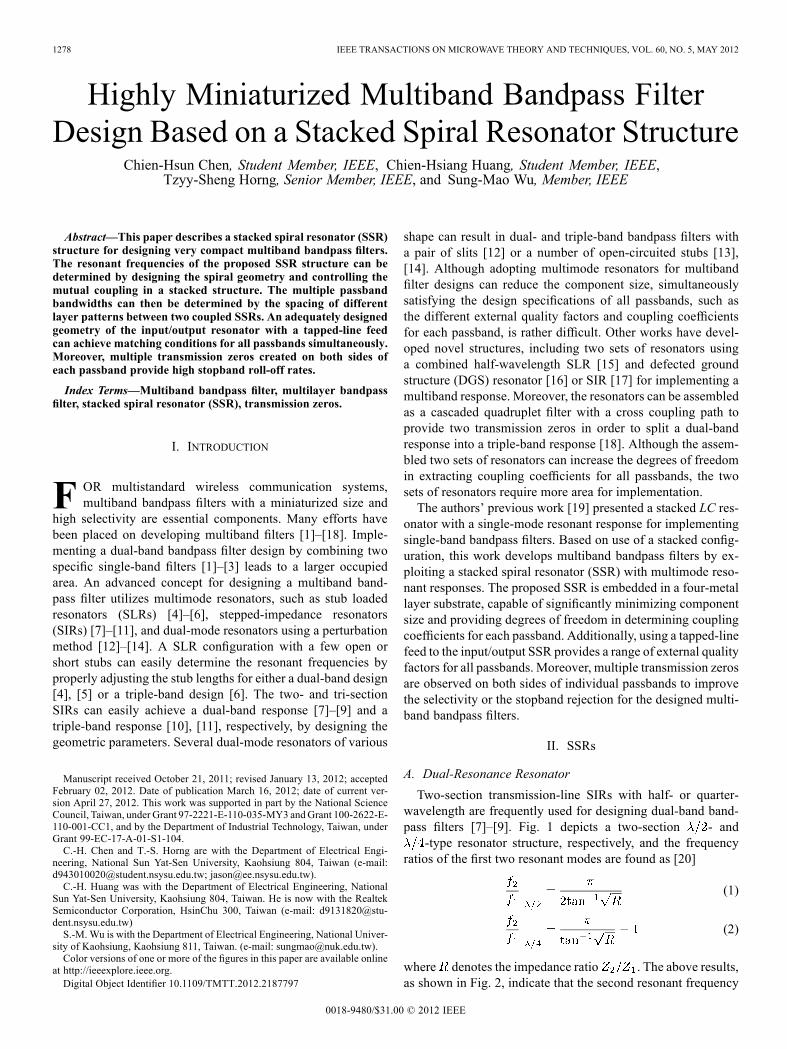
Fig. 10. Proposed dual-band bandpass filter design using two coupled dual-resonance SSRs. (a) 3-D geometrical configuration. (b) Top view layout andphotograph.
Fig. 11. Comparison of the magnitude of and between EM simulationand measurement for the proposed dual-band bandpass filter design.
change of only slightly impacts . Also, se-lect mm to obtain and pre-serve .
Fig. 10 shows the 3-D geometrical configuration, top viewlayout, and photograph of the designed second-order dual-bandbandpass filter. The occupied area, excluding the tapped line, is2.5 mm 1.8 mm, revealing an ultra-compact component sizecompared with conventional microstrip dual-band filters.Fig. 11 compares the magnitudes of and between
HFSS simulation and measurement, indicating a good agree-ment over a frequency range up to 8 GHz. The measured returnlosses in the two passbands exceed 19 dB. The insertion lossesare less than 1.2 and 1.7 dB in the first and second passband, re-spectively. The four transmission zeros located at 1.2, 3.2, 4.4,and 6.2 GHz enhance the rolloff rates on both sides of the twopassbands. These transmission zeros come from coexistence ofelectric and magnetic coupling [24] and depend on the spacing
and . For this case, and are given as 0.1and 0.18 mm, respectively. The four transmission-zero frequen-cies denoted as , for and , are discussed in detailas follows.A change in the spacing or the spacing causes a
frequency shift in the transmission-zero frequency .As , the transmission-zero frequency movestoward a higher frequency. In contrast, as , the
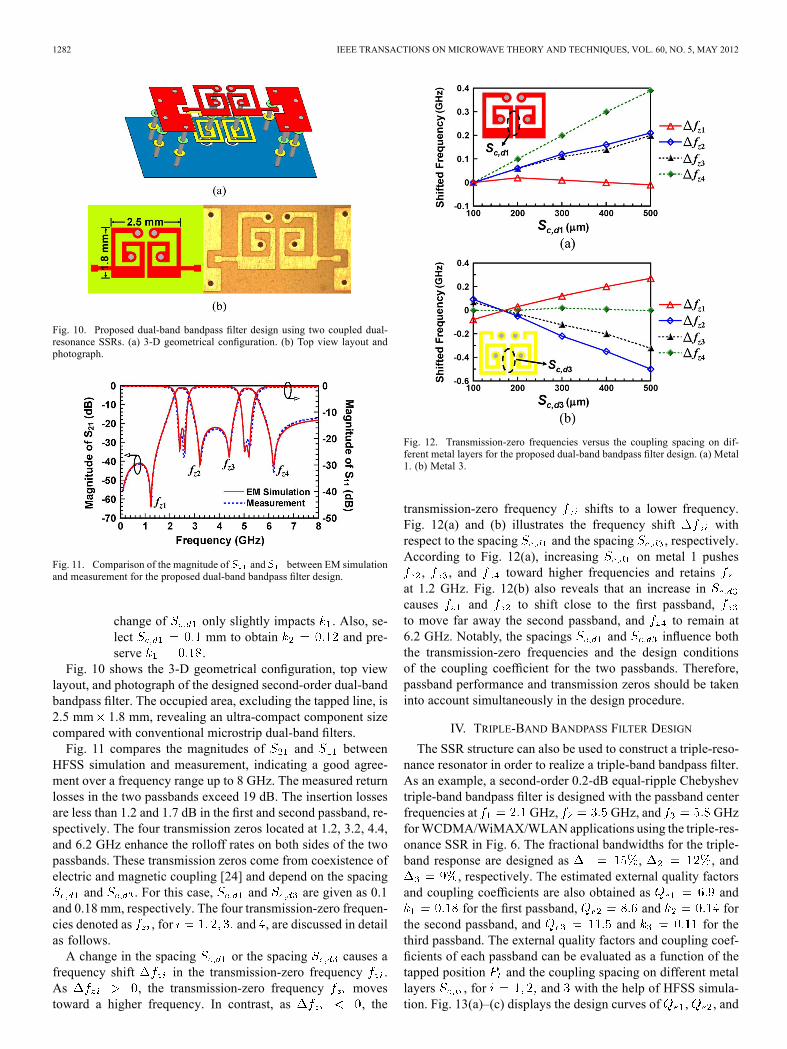
Fig. 12. Transmission-zero frequencies versus the coupling spacing on dif-ferent metal layers for the proposed dual-band bandpass filter design. (a) Metal1. (b) Metal 3.
transmission-zero frequency shifts to a lower frequency.Fig. 12(a) and (b) illustrates the frequency shift withrespect to the spacing and the spacing , respectively.According to Fig. 12(a), increasing on metal 1 pushes, , and toward higher frequencies and retains
at 1.2 GHz. Fig. 12(b) also reveals that an increase incauses and to shift close to the first passband,to move far away the second passband, and to remain at6.2 GHz. Notably, the spacings and influence boththe transmission-zero frequencies and the design conditionsof the coupling coefficient for the two passbands. Therefore,passband performance and transmission zeros should be takeninto account simultaneously in the design procedure.
IV. TRIPLE-BAND BANDPASS FILTER DESIGN
The SSR structure can also be used to construct a triple-reso-nance resonator in order to realize a triple-band bandpass filter.As an example, a second-order 0.2-dB equal-ripple Chebyshevtriple-band bandpass filter is designed with the passband centerfrequencies at GHz, GHz, and GHzforWCDMA/WiMAX/WLAN applications using the triple-res-onance SSR in Fig. 6. The fractional bandwidths for the triple-band response are designed as , , and
, respectively. The estimated external quality factorsand coupling coefficients are also obtained as and
for the first passband, and forthe second passband, and and for thethird passband. The external quality factors and coupling coef-ficients of each passband can be evaluated as a function of thetapped position and the coupling spacing on different metallayers , for and with the help of HFSS simula-tion. Fig. 13(a)–(c) displays the design curves of , , and

CHEN et al.: HIGHLY MINIATURIZED MULTIBAND BANDPASS FILTER DESIGN BASED ON SSR STRUCTURE 1283
Fig. 13. External quality factors versus the tapped feed position for the triple-resonance SSR. (a) Band 1. (b) Band 2. (c) Band3.
, respectively, with respect to for different combinationof the specified widths and on metal 1. According toFig. 13(a) and (c), an increase in increases the value of ,yet hardly changes the value of . Conversely, an increase in
enlarges the value of , yet barely affects the value of. Moreover, the change of or negligibly influences, as shown in Fig. 13(b). Therefore, can bemade smaller
or larger than and by increasing or decreasing bothand .To further explain Fig. 13 with an EM point of view, Fig. 14
shows the simulated current distribution on the triple-reso-nance SSR at the three main resonant frequencies. As shownin Fig. 14(a) and (c), the current distribution concentrateson the different portion of the metal-1 spiral pattern withdifferent width of and at the first and third resonantfrequency, respectively. It is therefore reasonable to observethat increasing enlarges rather than , whereasincreasing has the converse effect. Moreover, it can be seenfrom Fig. 14(b) that the currents mainly concentrate on metal 2and 3 and weaken on metal 1 at the second resonant frequency.
Fig. 14. Simulated current distribution on the triple-resonance SSR. (a) At thefirst resonant frequency. (b) At the second resonant frequency. (c) At the thirdresonant frequency.
This can explain why the change of the width and onthe metal-1 spiral pattern hardly influences .As a matter of fact, all of the external quality factors for a
triple-band response can be individually determined by the fol-lowing procedure: First, determine the tapped feed positionat the input/output resonator based on the calculated value of
; Second, determine the width from the design value of; Finally, determine the width from the estimated value
of . The next step determines the spacing in each layer toobtain the calculated coupling coefficients for each passband.Fig. 15(a)–(c) shows the design curves of the coupling coeffi-cients with respect to the spacing of onmetal 1, the spacing
on metal 2, and the spacing on metal 3, respectively.As mentioned earlier in the dual-band BPF design, the couplingcoefficients , , and corresponding to the first, second,and third passband, respectively, can also be individually deter-mined by adequately controlling the spacings , , and
. Moreover, an extra metallic stub on the right edge of theSSR on metal 1, as shown in Fig. 13, can be used to enhancethese coupling coefficients. The design procedure for the pro-posed triple-band bandpass filter is summarized as follows.1) Under the condition of mm and
mm in Fig. 13, choose the tapped feed position atmm to correspond to the external quality fac-
tors , , and forachieving the design requirement.
2) Fig. 15(c) shows the coupling coefficients versus thespacing on metal 3, while mm and
mm. Also, choose mm to ob-tain the coupling coefficient for the first pass-band.
3) Fig. 15(a) shows the coupling coefficients versus thespacing on metal 1, while mm and
mm since reveals a weak dependenceon . Also, choose mm to provide
for the third passband and preserve .4) Fig. 15(b) shows the coupling coefficients versus thespacing on metal 2 since and vary slightly

1284 IEEE TRANSACTIONS ON MICROWAVE THEORY AND TECHNIQUES, VOL. 60, NO. 5, MAY 2012
Fig. 15. Coupling coefficients versus the coupling spacing on differentmetal layers for the coupled triple-resonance SSRs. (a) Metal 1. (b) Metal 2.(c) Metal 3.
Fig. 16. Proposed triple-band bandpass filter design using two coupled triple-resonance SSRs. (a) 3-D geometrical configuration. (b) Top view layout andphotograph.
over a range of from 0.3 to 1 mm. Also, choosemm to obtain and retain
and simultaneously.
Fig. 17. Comparison of the magnitude of and between EM simulationand measurement for the proposed triple-band bandpass filter design.
Fig. 18. Transmission-zero frequencies versus the coupling spacing on dif-ferent metal layers for the proposed triple-band bandpass filter design. (a) Metal1. (b) Metal 2. (c) Metal 3.
Fig. 16 illustrates the 3-D geometrical configuration, top viewlayout, and photograph of the designed second-order triple-bandbandpass filter. The occupied area, excluding the tapped line, is2.9 mm 2.4 mm.Fig. 17 compares the magnitudes of and between
HFSS simulation and measurement for the proposed triple-bandbandpass filter design, indicating a good agreement over a fre-quency range up to 8 GHz. The measured insertion losses arelower than 1.4, 1.7, and 2 dB in the first, second, and third pass-band, respectively, while the measured return losses are all ex-ceed 15 dB. According to Fig. 17, each passband has a pair of
CHEN et al.: HIGHLY MINIATURIZED MULTIBAND BANDPASS FILTER DESIGN BASED ON SSR STRUCTURE 1285
transmission zeros on both sides. They are due to coexistence ofmagnetic and electric coupling and located at 0.9 and 2.4 GHzwith respect to the first passband, at 3 and 4.2 GHz with respectto the second passband, and at 5.2 and 7.2 GHz with respect tothe third passband.Similarly, varying the spacing , , and causes
a frequency shift in the transmission-zero frequency .The transmission-zero frequency also shifts to the higherand lower frequency for and , respectively.Fig. 18 illustrates the frequency shift versus the spacing
, , and . According to Fig. 18(a), increasingmoves the transmission-zero frequencies and close tothe third passband without altering the other transmission-zerofrequencies. Fig. 18(b) reveals that an increase in shiftsthe two transmission-zero frequencies and to lower fre-quencies, while the other ones only exhibit a slight change. Ac-cording to Fig. 18(c), an increase in shifts the transmis-sion-zero frequencies and that are on both sides of thefirst passband to higher frequencies. Meanwhile, the transmis-sion-zero frequencies and near the second passband arenearly unchanged, and the transmission-zero frequenciesand near the third passband are shifted toward lower fre-quencies. Notably, although adjusting , , or canflexibly move the transmission-zero frequencies, special care isnecessary to deal with the effects on coupling coefficients.
V. CONCLUSION
This paper has described very compact dual- and triple-bandbandpass filters based on SSRs. The resonant frequencies of theproposed SSRs depend on both the geometry of spiral patternsin different metal layers and the spacing between the adjacentspiral patterns in the same layer. The tapped-feed structure ap-plied to the proposed SSR with a spiral pattern of nonuniformwidth on metal 1 can flexibly provide an appropriate externalquality factor to achieve the impedancematching condition. Ad-ditionally, controlling the spacing between two spiral patternsin different metal layers offer superior degrees of freedom toindividually determine the bandwidth of each passband for amultiband bandpass filter design. Moreover, multiple transmis-sion zeros are created on both sides of each passband to signifi-cantly improve the roll-off rate and attenuation in the stopband.
REFERENCES
[1] X. Y. Zhang and Q. Xue, “Novel dual-mode dual-band filters usingcoplanar-waveguide-fed ring resonators,” IEEE Trans.Microw. TheoryTech., vol. 55, no. 10, pp. 2183–2190, Oct. 2007.
[2] E. E. Djoumessi and K. Wu, “Multilayer dual-mode dual-bandpassfilter,” IEEEMicrow. Wireless Compon. Lett., vol. 19, no. 1, pp. 21–23,Jan. 2009.
[3] X. Luo, H. Qian, J.-G. Ma, K. Ma, and K. S. Yeo, “Compact dual-band bandpass filters using novel embedded spiral resonator (ESR),”IEEE Microw. Wireless Compon. Lett., vol. 20, no. 8, pp. 435–437,Aug. 2010.
[4] P. Mondal and M. K. Mandal, “Design of dual-band bandpass filtersusing stub-loaded open-loop resonators,” IEEE Trans. Microw. TheoryTech., vol. 56, no. 1, pp. 150–155, Jan. 2008.
[5] Z. Zhang, Y.-C. Jiao, X.-M.Wang, and S.-F. Cao, “Design of a compactdual-band bandpass filter using opposite hook-shaped resonator,” IEEEMicrow. Wireless Compon. Lett., vol. 21, no. 7, pp. 359–361, Jul. 2011.
[6] Q.-X. Chu, F.-C. Chen, Z.-H. Tu, and H. Wang, “A novel crossed res-onator and its applications to bandpass filters,” IEEE Trans. Microw.Theory Tech., vol. 57, no. 7, pp. 1753–1759, Jul. 2009.
[7] P. K. Singh, S. Basu, and Y.-H. Wang, “Miniature dual-band filterusing quarter wavelength stepped impedance resonators,” IEEE Mi-crow. Wireless Compon. Lett., vol. 18, no. 2, pp. 88–90, Feb. 2008.
[8] Y.-C. Chang, C.-H. Kao, M.-H. Weng, and R.-Y. Yang, “Design of thecompact dual-band bandpass filter with high isolation for GPS/WLANapplications,” IEEE Microw. Wireless Compon. Lett., vol. 19, no. 12,pp. 780–782, Dec. 2009.
[9] C.-H. Tseng and H.-Y. Shao, “A new dual-band microstrip bandpassfilter using net-type resonators,” IEEE Microw. Wireless Compon.Lett., vol. 20, no. 4, pp. 196–198, Apr. 2010.
[10] C.-I. G. Hsu, C.-H. Lee, and Y.-H. Hsieh, “Tri-band bandpass filterwith sharp passband skirts designed using tri-section SIRs,” IEEE Mi-crow. Wireless Compon. Lett., vol. 18, no. 1, pp. 19–21, Jan. 2008.
[11] Q.-X. Chu and X.-M. Lin, “Advanced triple-band bandpass filter usingtri-section SIR,” Electron. Lett., vol. 44, no. 4, pp. 295–296, Feb. 2008.
[12] Y. Sung, “Dual-mode dual-band filter with band notch structures,”IEEE Microw. Wireless Compon. Lett., vol. 20, no. 2, pp. 73–75, Feb.2010.
[13] S. Luo, L. Zhu, and S. Sun, “A dual-band ring-resonator bandpass filterbased on two pairs of degenerate modes,” IEEE Trans. Microw. TheoryTech., vol. 58, no. 12, pp. 3427–3432, Dec. 2010.
[14] S. Luo, L. Zhu, and S. Sun, “Compact dual-mode triple-band bandpassfilters using three pairs of degenerate modes in a ring resonator,” IEEETrans. Microw. Theory Tech., vol. 59, no. 5, pp. 1222–1229, May 2011.
[15] X. Y. Zhang, Q. Xue, and B. J. Hu, “Planar tri-band bandpass filter withcompact size,” IEEE Microw. Wireless Compon. Lett., vol. 20, no. 5,pp. 262–264, May 2010.
[16] X. Lai, C.-H. Liang, H. Di, and B. Wu, “Design of tri-band filter basedon stub loaded resonator and DGS resonator,” IEEE Microw. WirelessCompon. Lett., vol. 20, no. 5, pp. 265–267, May 2010.
[17] M. Zhou, X. Tang, and F. Xiao, “Compact dual band transversalbandpass filter with multiple transmission zeros and controllablebandwidths,” IEEE Microw. Wireless Compon. Lett., vol. 19, no. 6,pp. 347–349, Jun. 2009.
[18] B.-J. Chen, T.-M. Shen, and R.-B. Wu, “Design of tri-band filters withimproved band allocation,” IEEE Trans. Microw. Theory Tech., vol.57, no. 7, pp. 1790–1797, Jul. 2009.
[19] C.-H. Chen, C.-H. Huang, T.-S. Horng, S.-M. Wu, J.-Y. Li, C.-C.Chen, C.-T. Chiu, and C.-P. Hung, “Very compact stackedresonator-based bandpass filters with a novel approach to tune thetransmission zeros,” IEEE Microw. Wireless Compon. Lett., vol. 19,no. 5, pp. 293–295, May 2009.
[20] M. Sagawa, M. Makimoto, and S. Yamashita, “Geometrical structuresand fundamental characteristics of microwave stepped-impedanceresonators,” IEEE Trans. Microw. Theory Tech., vol. 45, no. 7, pp.1078–1085, Jul. 1997.
[21] D. Packiaraj, M. Ramesh, and A.-T. Kalghatgi, “Design of a tri-sectionfolded SIR filter,” IEEE Microw. Wireless Compon. Lett., vol. 16, no.5, pp. 317–319, May 2006.
[22] C.-H. Lee, C.-I. G. Hsu, and L.-Y. Chen, “Band-notched ultra-wide-band bandpass filter design using combined modified quarter-wave-length tri-section stepped-impedance resonator,” IET Microw.Antennas Propag., vol. 3, no. 8, pp. 1232–1236, Dec. 2009.
[23] J.-S. Hong and M. J. Lancaster, Microstrip Filters for RF/MicrowaveApplications. New York: Wiley, 2001, pp. 109–272.
[24] Q.-X. Chu and H. Wang, “A compact open-loop filter with mixed elec-tric and magnetic coupling,” IEEE Trans. Microw. Theory Tech., vol.56, no. 2, pp. 431–439, Feb. 2008.
Chien-Hsun Chen (S’08) was born January 30,1981, in Kaohsiung, Taiwan. He received theB.S.E.E degree from the Yuan-Ze University,Taoyuan, Taiwan, in 2003, the M.S.E.E. degree fromI-Shou University, Kaohsiung, Taiwan, in 2005,and is currently working toward the Ph.D. degreein electrical engineering at National Sun Yet-SenUniversity, Kaohsiung, Taiwan.His research interests are the design and analysis
of embedded and integrated passive components forwireless communications.

1286 IEEE TRANSACTIONS ON MICROWAVE THEORY AND TECHNIQUES, VOL. 60, NO. 5, MAY 2012
Chien-Hsiang Huang (S’08) was born August24, 1978, in Kaohsiung, Taiwan. He received theB.S.E.E., M.S.E.E., and Ph D. degrees from NationalSun Yat-Sen University, Kaohsiung, Taiwan, in2000, 2002, and 2011, respectively.He is currently a Research and Development En-
gineer with the Realtek Semiconductor Corporation,HsinChu, Taiwan. His main research interests are de-sign and modeling of RF/microwave integrated pas-sive devices.
Tzyy-Sheng Horng (S’88–M’92–SM’05) wasborn in Taichung, Taiwan, on December 7, 1963.He received the B.S.E.E. degree from NationalTaiwan University, Taipei, Taiwan, in 1985, and theM.S.E.E. and Ph.D. degrees from the Universityof California at Los Angeles (UCLA), in 1990 and1992, respectively.Since August 1992, he has been with the Depart-
ment of Electrical Engineering, National SunYat-SenUniversity, Kaohsiung, Taiwan, where he was the Di-rector of the Telecommunication Research and De-
velopment Center (2003–2008) and Director of the Institute of Communica-tions Engineering (2004–2007), and where he is currently a Professor and theAdvanced Semiconductor Engineering Inc. (ASE Inc.) Chair Professor. He hasauthored or coauthored over 100 technical publications published in IEEE jour-nals and conferences proceedings. He holds over ten patents. His research inter-ests include RF and microwave integrated circuits and components, RF signalintegrity for wireless system-in-package, digitally assisted RF technologies, andgreen radios for cognitive sensors and Doppler radars.
Dr. Horng has served on several Technical Program Committees of interna-tional conferences including the International Association of Science and Tech-nology for Development (IASTED), International Conference on Wireless andOptical Communications, the IEEE Region 10 International Technical Confer-ence, the IEEE International Workshop on Electrical Design of Advanced Pack-aging and Systems, the Asia–Pacific Microwave Conference, the IEEE RadioandWireless Symposium, and the Electronic Components and Technology Con-ference. He was the recipient of the 1996 Young Scientist Award presented bythe International Union of Radio Science, the 1998 Industry–Education Coop-eration Award presented by the Ministry of Education, Taiwan, and the 2010Distinguished Electrical Engineer Award presented by the Chinese Institute ofElectrical Engineering, Taiwan.
Sung-Mao Wu (M’96) was born in Kaohsiung,Taiwan, on January 29, 1971. He received theM.S.E.E. degree from the Yulin University ofScience and Technology, Yulin, Taiwan, in 1996,and the Ph.D. degree from National Sun Yet-SenUniversity, Kaohsiung, Taiwan, in 2001.From July 2000 to March 2006, he was with the
Research and Development Electrical Laboratory,Advance Semiconductor Engineering (ASE), incharge of system-in-package (SiP) circuit designand analysis. Since April 2006, he has been with
the Department of Electrical Engineering, National University of Kaohsiung,Kaohsiung, Taiwan, initially as an Assistant Professor, and currently as anassociate Professor. His research fields are in the 3-D SiP (3-D-SiP) and RFintegrated circuit (RFIC) design and testing technologies.


![+1cm[width=30mm]logo.pdf +1cm Bandpass Sampling ... · i Bandpass Sampling Methodology for Uniformly Spaced, Multiband, Energy-Sparse Spectrum By Tauqeer Ahmed (PE113003) Prof. Dr.](https://static.fdocuments.us/doc/165x107/5f8d86f4da047a6a023e45e4/1cmwidth30mmlogopdf-1cm-bandpass-sampling-i-bandpass-sampling-methodology.jpg)


