High Temp Ceramic.pdf
28
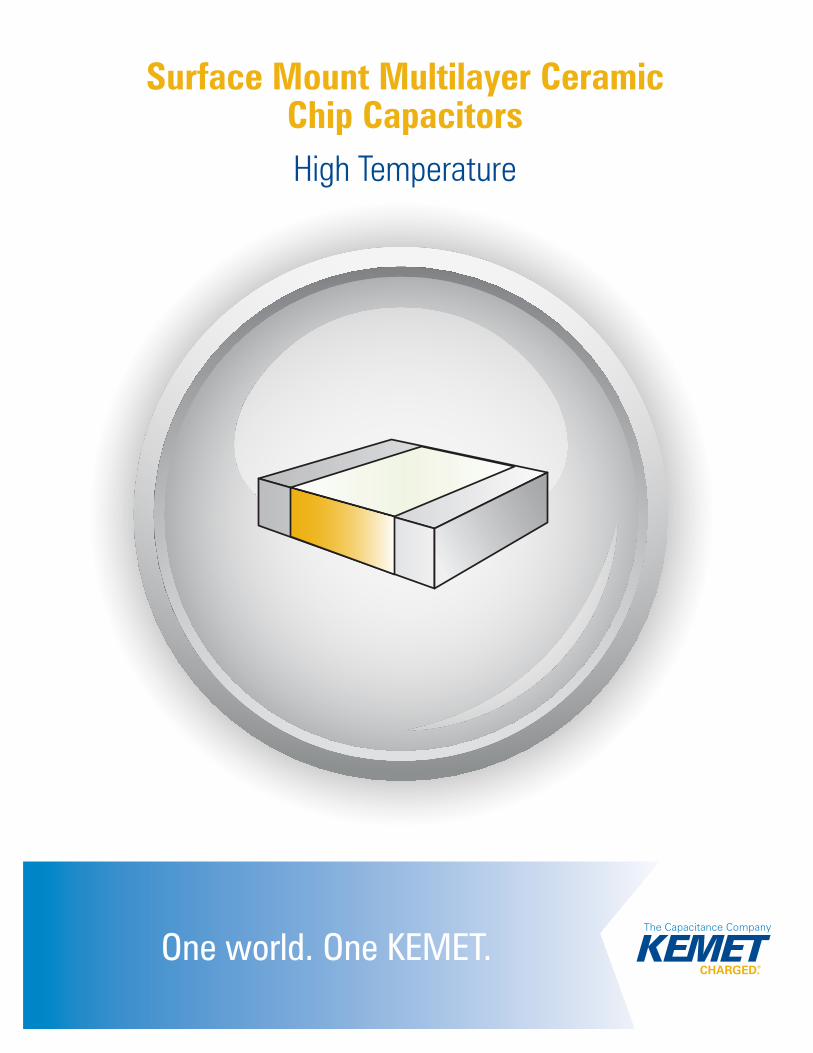
One world. One KEMET. Surface Mount Multilayer Ceramic Chip Capacitors High Temperature
-
Upload
dovesnestin -
Category
Documents
-
view
38 -
download
0
description
capacitors
Transcript of High Temp Ceramic.pdf
One world. One KEMET. Ceramic Through-holeCeramic surface mount
Tantalum surface mount
Tantalum Through-holeTantalum Through-hole
Aluminum Electrolytic
Aluminum surface mount
Aluminum Electrolytic Capacitors Snap IN
Film & ElectPoly Pulse High Freq
Power and AC Film CapMotor Run
Surface Mount Film Cap
Surface Mount Multilayer Ceramic Chip CapacitorsHigh Temperature
© KEMET Electronics Corporation • P.O. Box 5928 • Greenville, SC 29606 (864) 963-6300 • www.kemet.com CC105-1 • 10/16/2010 1One WORLD One Brand One Strategy One Focus One Team One KEMET
Surface Mount Multilayer Ceramic Chip Capacitors
High Temperature
Table of Contents ___________________________________________________ Page
• High Temperature (150°C) X8L Dielectric, 10VDC-50VDC (Commercial & Automotive Grade) ___2 • Performance & Reliability: Test Methods and Conditions __________________________5 • High Temperature (150°C) Ultra-Stable X8R Dielectric, 25VDC-100VDC (Commercial & Automotive Grade) ____________________________________________6 • Performance & Reliability: Test Methods and Conditions __________________________10 • High Temperature (200°C), C0G Dielectric, 10VDC-200VDC (Commercial Grade) _____________11 • Performance & Reliability: Test Methods and Conditions __________________________16
• Chip Thickness / Packaging Quantities ______________________________________________17 • Soldering Process _______________________________________________________________18 • Land Pattern Design Recommendations _____________________________________________18 • Packaging _____________________________________________________________________19 • Marking _______________________________________________________________________25 • Other KEMET Resources _________________________________________________________26 • KEMET Addresses ______________________________________________________________27
© KEMET Electronics Corporation • P.O. Box 5928 • Greenville, SC 29606 (864) 963-6300 • www.kemet.com CC105-1 • 10/16/2010 2© KEMET Electronics Corporation • P.O. Box 5928 • Greenville, SC 29606 (864) 963-6300 • www.kemet.com C1008-1 • 10/19/2010 1One WORLD One Brand One Strategy One Focus One Team One KEMET
Benefi ts• -55°C to +150°C operating temperature range• Pb-Free and RoHS compliant (excluding SnPb end metallization
option)• EIA 0402, 0603, 0805, 1206 and 1210 case sizes• DC voltage ratings of 10V, 25V and 50V• Capacitance offerings ranging from .012μF to 10μF• Available capacitance tolerances of ±5%, ±10% and ±20%• Commercial and automotive grades available• Non-polar device, minimizing installation concerns• 100% pure matte tin-plated end metallization allowing for
excellent solderability• SnPb plated end metallization option available upon request
(5% min)
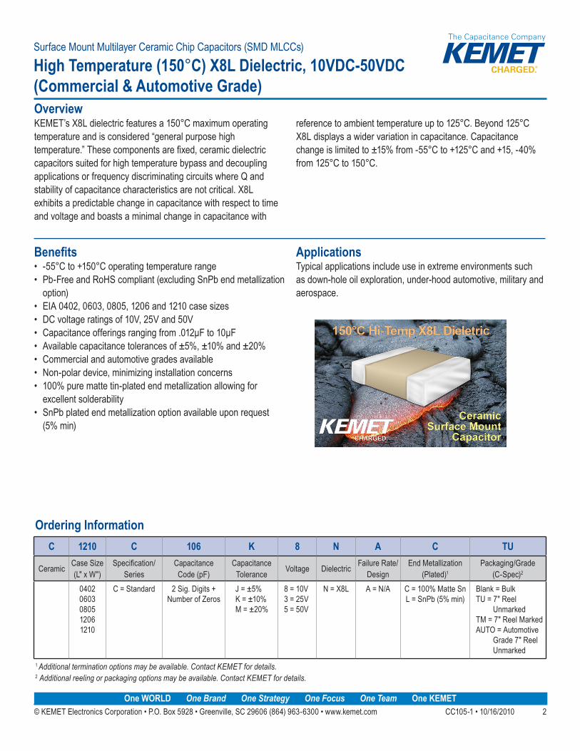
ApplicationsTypical applications include use in extreme environments such as down-hole oil exploration, under-hood automotive, military and aerospace.
OverviewKEMET’s X8L dielectric features a 150°C maximum operating temperature and is considered “general purpose high temperature.” These components are fi xed, ceramic dielectric capacitors suited for high temperature bypass and decoupling applications or frequency discriminating circuits where Q and stability of capacitance characteristics are not critical. X8L exhibits a predictable change in capacitance with respect to time and voltage and boasts a minimal change in capacitance with
reference to ambient temperature up to 125°C. Beyond 125°C X8L displays a wider variation in capacitance. Capacitance change is limited to ±15% from -55°C to +125°C and +15, -40% from 125°C to 150°C.
Surface Mount Multilayer Ceramic Chip Capacitors (SMD MLCCs)
High Temperature (150°C) X8L Dielectric, 10VDC-50VDC(Commercial & Automotive Grade)
1 Additional termination options may be available. Contact KEMET for details. 2 Additional reeling or packaging options may be available. Contact KEMET for details.
Ordering InformationC 1210 C 106 K 8 N A C TU
Ceramic Case Size (L" x W")
Specifi cation/Series
Capacitance Code (pF)
Capacitance Tolerance Voltage Dielectric Failure Rate/
DesignEnd Metallization
(Plated)1Packaging/Grade
(C-Spec)2
04020603080512061210
C = Standard 2 Sig. Digits + Number of Zeros
J = ±5%K = ±10%M = ±20%
8 = 10V3 = 25V5 = 50V
N = X8L A = N/A C = 100% Matte SnL = SnPb (5% min)
Blank = BulkTU = 7" Reel
UnmarkedTM = 7" Reel MarkedAUTO = Automotive
Grade 7" Reel Unmarked
© KEMET Electronics Corporation • P.O. Box 5928 • Greenville, SC 29606 (864) 963-6300 • www.kemet.com CC105-1 • 10/16/2010 3
Surface Mount Multilayer Ceramic Chip Capacitors – High Temperature
© KEMET Electronics Corporation • P.O. Box 5928 • Greenville, SC 29606 (864) 963-6300 • www.kemet.com C1008-1 • 10/19/2010 2
SMD MLCCs – High Temperature (150°C) X8L Dielectric, 10VDC-50VDC (Commercial & Automotive Grade)
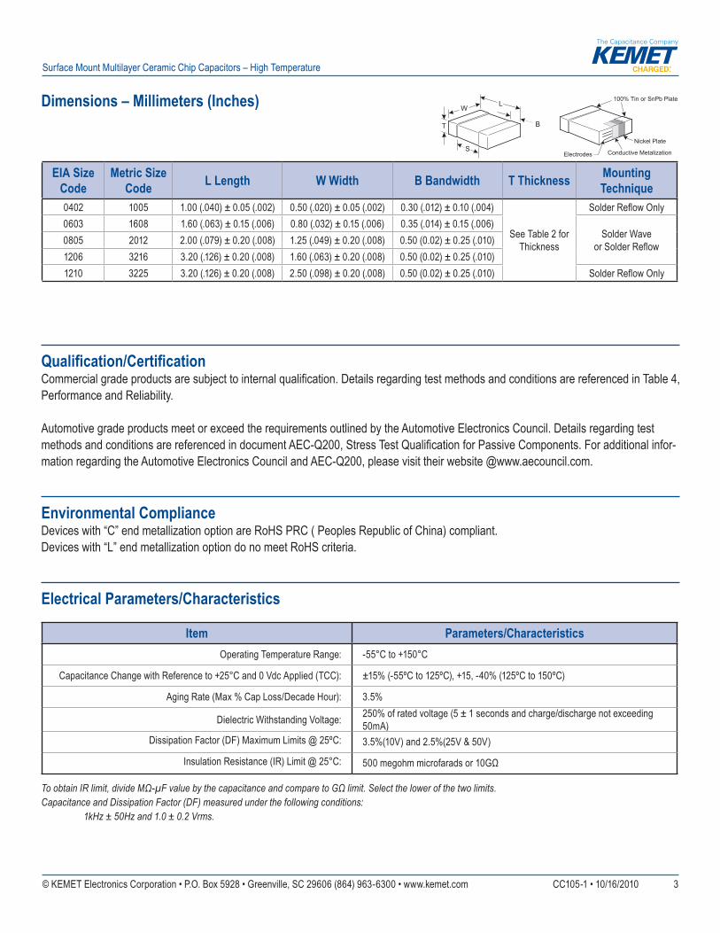
Dimensions – Millimeters (Inches)
Qualifi cation/Certifi cationCommercial grade products are subject to internal qualifi cation. Details regarding test methods and conditions are referenced in Table 4, Performance and Reliability.
Automotive grade products meet or exceed the requirements outlined by the Automotive Electronics Council. Details regarding test methods and conditions are referenced in document AEC-Q200, Stress Test Qualifi cation for Passive Components. For additional infor-mation regarding the Automotive Electronics Council and AEC-Q200, please visit their website @www.aecouncil.com.
Environmental ComplianceDevices with “C” end metallization option are RoHS PRC ( Peoples Republic of China) compliant. Devices with “L” end metallization option do no meet RoHS criteria.
Electrical Parameters/Characteristics
Item Parameters/CharacteristicsOperating Temperature Range: -55°C to +150°C
Capacitance Change with Reference to +25°C and 0 Vdc Applied (TCC): ±15% (-55ºC to 125ºC), +15, -40% (125ºC to 150ºC)
Aging Rate (Max % Cap Loss/Decade Hour): 3.5%
Dielectric Withstanding Voltage: 250% of rated voltage (5 ± 1 seconds and charge/discharge not exceeding 50mA)
Dissipation Factor (DF) Maximum Limits @ 25ºC: 3.5%(10V) and 2.5%(25V & 50V)
Insulation Resistance (IR) Limit @ 25°C: 500 megohm microfarads or 10GΩ
To obtain IR limit, divide MΩ-µF value by the capacitance and compare to GΩ limit. Select the lower of the two limits.Capacitance and Dissipation Factor (DF) measured under the following conditions: 1kHz ± 50Hz and 1.0 ± 0.2 Vrms.
EIA Size Code
Metric Size Code L Length W Width B Bandwidth T Thickness Mounting
Technique0402 1005 1.00 (.040) ± 0.05 (.002) 0.50 (.020) ± 0.05 (.002) 0.30 (.012) ± 0.10 (.004)
See Table 2 for Thickness
Solder Refl ow Only0603 1608 1.60 (.063) ± 0.15 (.006) 0.80 (.032) ± 0.15 (.006) 0.35 (.014) ± 0.15 (.006)
Solder Waveor Solder Refl ow0805 2012 2.00 (.079) ± 0.20 (.008) 1.25 (.049) ± 0.20 (.008) 0.50 (0.02) ± 0.25 (.010)
1206 3216 3.20 (.126) ± 0.20 (.008) 1.60 (.063) ± 0.20 (.008) 0.50 (0.02) ± 0.25 (.010)1210 3225 3.20 (.126) ± 0.20 (.008) 2.50 (.098) ± 0.20 (.008) 0.50 (0.02) ± 0.25 (.010) Solder Refl ow Only
Cer
amic
Su
rfac
e M
ou
nt
W L
T B
S
100% Tin or SnPb Plate
Nickel Plate
Conductive MetalizationElectrodes

© KEMET Electronics Corporation • P.O. Box 5928 • Greenville, SC 29606 (864) 963-6300 • www.kemet.com CC105-1 • 10/16/2010 4
Surface Mount Multilayer Ceramic Chip Capacitors – High Temperature
Table 1 – X8L Dielectric, (0201 - 1206 Case Sizes)
UD = Under Development, xx¹ Available only in K,M tolerance, xx² Available only in M tolerance.
© KEMET Electronics Corporation • P.O. Box 5928 • Greenville, SC 29606 (864) 963-6300 • www.kemet.com C1008-1 • 10/19/2010 3
SMD MLCCs – High Temperature (150°C) X8L Dielectric, 10VDC-50VDC (Commercial & Automotive Grade)
Table 1 – (0402 - 1210 Case Sizes)
Cap Cap Code
Series C0402 C0603 C0805 C1206 C1210Voltage Code 8 3 8 3 5 8 3 5 8 3 5 8 3 5
Voltage DC 10 25 10 25 50 10 25 50 10 25 50 10 25 50
Cap Tolerance Product Availability and Chip Thickness Codes See Table 2 for Chip Thickness Dimensions12,000 pF 123 J K M BB BB15,000 pF 153 J K M BB BB18,000 pF 183 J K M BB BB22,000 pF 223 J K M BB BB27,000 pF 273 J K M BB33,000 pF 333 J K M BB39,000 pF 393 J K M BB47,000 pF 473 J K M BB CB CB CB56,000 pF 563 J K M68,000 pF 683 J K M82,000 pF 823 J K M
0.10 uF 104 J K M0.12 uF 124 J K M CB CB0.15 uF 154 J K M CB CB DG DG DG0.18 uF 184 J K M CB DG DG DG0.22 uF 224 J K M CB DD DD DG0.27 uF 274 J K M DD DD0.33 uF 334 J K M DD DD0.39 uF 394 J K M DE DE FD FD FD0.47 uF 474 J K M DE DE EG EG EG FD FD FD0.56 uF 564 J K M DG DH FF FF FF0.68 uF 684 J K M DG DH FG FG FG0.82 uF 824 J K M DG FL FL FL1.0 uF 105 J K M DG ED ED FM FM FM1.2 uF 125 J K M EH EH FG FG1.5 uF 155 J K M EH EH FG FG1.8 uF 185 J K M EF EH FG FG2.2 uF 225 J K M EF EH FG FG2.7 uF 275 J K M EH FG FH3.3 uF 335 J K M EH FM FM3.9 uF 395 J K M EH FG FK4.7 uF 475 J K M EH FG FS5.6 uF 565 J K M FH6.8 uF 685 J K M FM8.2 uF 825 J K M FK10 uF 106 J K M FS
Cap Cap Code
Voltage DC 10 25 10 25 50 10 25 50 10 25 50 10 25 50
Voltage Code 8 3 8 3 5 8 3 5 8 3 5 8 3 5
Series C0402 C0603 C0805 C1206 C1210
Roll Over forOrder Info.
C 1210 C 106 K 8 N A C TU
Ceramic Case Size (L" x W")
Specifi cation/Series
Capacitance Code (pF)
Capacitance Tolerance Voltage Dielectric Failure Rate/
DesignEnd Metallization
(Plated)1Packaging/Grade
(C-Spec)2
04020603080512061210
C = Standard 2 Sig. Digits + Number of Zeros
J = ±5%K = ±10%M = ±20%
8 = 10V3 = 25V5 = 50V
N = X8L A = N/A C = 100% Matte SnL = SnPb (5% min)
Blank = BulkTU = 7" Reel
UnmarkedTM = 7" Reel MarkedAUTO = Automotive
Grade 7" Reel Unmarked

© KEMET Electronics Corporation • P.O. Box 5928 • Greenville, SC 29606 (864) 963-6300 • www.kemet.com CC105-1 • 10/16/2010 5
Surface Mount Multilayer Ceramic Chip Capacitors – High Temperature
© KEMET Electronics Corporation • P.O. Box 5928 • Greenville, SC 29606 (864) 963-6300 • www.kemet.com C1008-1 • 10/19/2010 6
SMD MLCCs – High Temperature (150°C) X8L Dielectric, 10VDC-50VDC (Commercial & Automotive Grade)
Table 4 – Performance & Reliability: Test Methods and ConditionsStress Reference Test or Inspection Method
Ripple Current Heat Generation∆T : 20ºC max.
Refl ow solder the capacitor onto a PC board and apply voltage with 10kHz~1Mhz sine curve. (Ripple voltage must be < rated voltage)
Terminal Strength JIS-C-6429 Appendix 1, Note: Force of 1.8kg for 60 seconds.
Board Flex JIS-C-6429 Appendix 2, Note: 2mm (min) for all except 3mm for C0G.
Solderability J-STD-002
Magnifi cation 50X. Conditions:
a) Method B, 4 hrs @ 155°C, dry heat @ 235°C
b) Method B @ 215°C category 3
c) Method D, category 3 @ 260°C
Temperature Cycling JESD22 Method JA-104 1000 Cycles (-55°C to +150°C), Measurement at 24 hrs. +/- 2 hrs after test conclusion.
Biased Humidity MIL-STD-202 Method 103
Load Humidity: 1000 hours 85°C/85%RH and Rated Voltage. Add 100K ohm resistor. Measurement at 24 hrs. +/- 2 hrs after test conclusion.Low Volt Humidity: 1000 hours 85C°/85%RH and 1.5V. Add 100K ohm resistor. Measurement at 24 hrs. +/- 2 hrs after test conclusion.
Moisture Resistance MIL-STD-202 Method 106 t = 24 hours/cycle. Steps 7a & 7b not required. Unpowered. Measurement at 24 hrs. +/- 2 hrs after test conclusion.
Thermal Shock MIL-STD-202 Method 107 -55°C/+150. Note: Number of cycles required-300, Maximum transfer time-20 seconds, Dwell time-15 minutes. Air-Air.
High Temperature Life MIL-STD-202 Method 108 1000 hours at 150°C with 1.5X rated voltage applied.
Storage Life MIL-STD-202 Method 108 150°C, 0VDC, for 1000 Hours.
Mechanical Shock MIL-STD-202 Method 213 Figure 1 of Method 213, Condition F.
Resistance to Solvents MIL-STD-202 Method 215 Add Aqueous wash chemical - OKEM Clean or equivalent.
Performance & Reliability: Test Methods and Conditions – X8L Dielectric

© KEMET Electronics Corporation • P.O. Box 5928 • Greenville, SC 29606 (864) 963-6300 • www.kemet.com CC105-1 • 10/16/2010 6© KEMET Electronics Corporation • P.O. Box 5928 • Greenville, SC 29606 (864) 963-6300 • www.kemet.com C1007-1 • 10/19/2010 7One WORLD One Brand One Strategy One Focus One Team One KEMET
Benefi ts• -55°C to +150°C operating temperature range• Pb-Free and RoHS compliant (excluding SnPb end metallization
option)• EIA 0402, 0603, 0805, 1206, 1210 & 1812 case sizes• DC voltage ratings of 25V, 50V and 100V• Capacitance offerings ranging from 100pF to 0.22μF• Available capacitance tolerances of ±1%, ±2%, ±5%, ±10% & ±20%• Extremely low ESR and ESL• High thermal stability• High ripple current capability• No capacitance change with respect to applied rated DC voltage• Non-polar device, minimizing installation concerns• Offered in both commercial and automotive grades • 100% pure matte tin-plated end metallization that allowing for
excellent solderability.• SnPb plated end metallization option available upon request (5% min)
ApplicationsTypical applications include decoupling, bypass and fi ltering in extreme environments such as down-hole oil exploration, under-hood automotive, military and aerospace.
OverviewKEMET’s Ultra-Stable X8R dielectric features a 150°C maximum operating temperature, offering the latest in high temperature dielectric technology and reliability for extreme temperature applications. It offers the same temperature capability as conventional X8R, but without the capacitance loss due to applied DC voltage. Ultra-Stable X8R exhibits no change in capacitance with respect to voltage and boasts a minimal change in capacitance with reference to ambient temperature. It is a suitable
replacement for higher capacitance and larger footprint devices that fail to offer capacitance stability. Capacitance change with respect to temperature is limited to ±15% from -55°C to +150°C.
Surface Mount Multilayer Ceramic Chip Capacitors (SMD MLCCs)
High Temperature (150°C) Ultra-Stable X8R Dielectric,25VDC-100VDC (Commercial & Automotive Grade)
1 Additional termination options may be available. Contact KEMET for details.2 Additional reeling or packaging options may be available. Contact KEMET for details.
Ordering Information
C 1210 C 184 K 3 H A C AUTO
Ceramic Case Size (L" x W")
Specifi cation/Series
Capacitance Code (pF)
Capacitance Tolerance Voltage Dielectric Failure Rate/
DesignEnd Metallization
(Plated)1
Packaging/Grade (C-Spec)2
040206030805120612101812
C = Standard 2 Sig. Digits + Number of Zeros
F = ±1%G = ±2%J = ±5%K = ±10%M = ±20%
3 = 25V5 = 50V1 = 100V
H = Ultra Stable X8R
A = N/A C = 100% Matte SnL = SnPb (5% min)
Blank = BulkTU = 7" Reel
UnmarkedTM = 7" Reel
MarkedAUTO = Automotive
Grade 7"Reel Unmarked

© KEMET Electronics Corporation • P.O. Box 5928 • Greenville, SC 29606 (864) 963-6300 • www.kemet.com CC105-1 • 10/16/2010 7
Surface Mount Multilayer Ceramic Chip Capacitors – High Temperature
© KEMET Electronics Corporation • P.O. Box 5928 • Greenville, SC 29606 (864) 963-6300 • www.kemet.com C1007-1 • 10/19/2010 8
SMD MLCCs – High Temperature (150°C) Ultra-Stable X8R Dielectric, 25VDC-100VDC (Commercial & Automotive Grade)
Dimensions – Millimeters (Inches)
Qualifi cation/Certifi cationCommercial grade products are subject to internal qualifi cation. Details regarding test methods and conditions are referenced in Table 4, Performance and Reliability.
Automotive grade products meet or exceed the requirements outlined by the Automotive Electronics Council. Details regarding test methods and conditions are referenced in document AEC-Q200, Stress Test Qualifi cation for Passive Components. For additional infor-mation regarding the Automotive Electronics Council and AEC-Q200, please visit their website @www.aecouncil.com.
Environmental ComplianceDevices with “C” end metallization option are RoHS PRC ( Peoples Republic of China) compliant. Devices with “L” end metallization option do no meet RoHS criteria.
Electrical Parameters/Characteristics
Item Parameters/CharacteristicsOperating Temperature Range: -55°C to +150°C
Capacitance Change with Reference to +25°C and 0 Vdc Applied (TCC): ±15%
Aging Rate (Max % Cap Loss/Decade Hour): 0%
Dielectric Withstanding Voltage: 250% of rated voltage (5 ± 1 seconds and charge/discharge not exceeding 50mA)
Dissipation Factor (DF) Maximum Limits @ 25ºC: 2.5%
Insulation Resistance (IR) Limit @ 25°C: 1000 megohm microfarads or 100GΩ
To obtain IR limit, divide MΩ-µF value by the capacitance and compare to GΩ limit. Select the lower of the two limits.Capacitance and Dissipation Factor (DF) measured under the following conditions: 1kHz ± 50Hz and 1.0 ± 0.2 Vrms.
Cer
amic
Su
rfac
e M
ou
nt
W L
T B
S
100% Tin or SnPb Plate
Nickel Plate
Conductive MetalizationElectrodes
EIA Size Code
Metric Size Code L Length W Width B Bandwidth T Thickness Mounting
Technique0402 1005 1.00 (.040) ± 0.05 (.002) 0.50 (.020) ± 0.05 (.002) 0.30 (.012) ± 0.10 (.004)
See Table 2 for Thickness
Solder Refl ow Only0603 1608 1.60 (.063) ± 0.15 (.006) 0.80 (.032) ± 0.15 (.006) 0.35 (.014) ± 0.15 (.006)
Solder Wave or Solder Refl ow0805 2012 2.00 (.079) ± 0.20 (.008) 1.25 (.049) ± 0.20 (.008) 0.50 (0.02) ± 0.25 (.010)
1206 3216 3.20 (.126) ± 0.20 (.008) 1.60 (.063) ± 0.20 (.008) 0.50 (0.02) ± 0.25 (.010)1210 3225 3.20 (.126) ± 0.20 (.008) 2.50 (.098) ± 0.20 (.008) 0.50 (0.02) ± 0.25 (.010)
Solder Refl ow Only1812 4532 4.50 (.177) ± 0.30 (.012) 3.20 (.126) ± 0.30 (.012) 0.60 (.024) ± 0.35 (.014)

© KEMET Electronics Corporation • P.O. Box 5928 • Greenville, SC 29606 (864) 963-6300 • www.kemet.com CC105-1 • 10/16/2010 8
Surface Mount Multilayer Ceramic Chip Capacitors – High Temperature
Table 1 – X8R Dielectric, (0402 - 1812 Case Sizes)
Cap Cap Code
Series C0402 C0603 C0805 C1206 C1210 C1812Voltage Code 3 5 1 3 5 1 3 5 1 3 5 1 3 5 1 5 1
Voltage DC 25 50 100 25 50 100 25 50 100 25 50 100 25 50 100
50 100
Cap Tolerance Product Availability and Chip Thickness Codes See Table 2 for Chip Thickness Dimensions100 pF 101 F G J K M BB BB BB110 pF 111 F G J K M BB BB BB120 pF 121 F G J K M BB BB BB130 pF 131 F G J K M BB BB BB150 pF 151 F G J K M BB BB BB160 pF 161 F G J K M BB BB BB180 pF 181 F G J K M BB BB BB200 pF 201 F G J K M BB BB BB220 pF 221 F G J K M BB BB BB240 pF 241 F G J K M BB BB BB270 pF 271 F G J K M BB BB BB300 pF 301 F G J K M BB BB BB330 pF 331 F G J K M BB BB BB360 pF 361 F G J K M BB BB BB390 pF 391 F G J K M BB BB BB430 pF 431 F G J K M BB BB BB CB CB CB470 pF 471 F G J K M BB BB BB CB CB CB510 pF 511 F G J K M BB BB BB CB CB CB560 pF 561 F G J K M BB BB BB CB CB CB620 pF 621 F G J K M BB BB BB CB CB CB680 pF 681 F G J K M BB BB BB CB CB CB750 pF 751 F G J K M BB BB BB CB CB CB820 pF 821 F G J K M BB BB BB CB CB CB910 pF 911 F G J K M BB BB BB CB CB CB
1,000 pF 102 F G J K M BB BB BB CB CB CB1,100 pF 112 F G J K M BB BB CB CB CB1,200 pF 122 F G J K M BB BB CB CB CB1,300 pF 132 F G J K M BB BB CB CB CB1,500 pF 152 F G J K M BB BB CB CB CB1,600 pF 162 F G J K M CB CB CB1,800 pF 182 F G J K M CB CB CB2,000 pF 202 F G J K M CB CB CB2,200 pF 222 F G J K M CB CB CB DC DC DC2,400 pF 242 F G J K M CB CB CB DC DC DC2,700 pF 272 F G J K M CB CB CB DC DC DC3,000 pF 302 F G J K M CB CB CB DC DC DC3,300 pF 332 F G J K M CB CB CB DC DC DC3,600 pF 362 F G J K M CB CB CB DC DC DC3,900 pF 392 F G J K M CB CB CB DC DC DC4,300 pF 432 F G J K M CB CB CB DC DC DC4,700 pF 472 F G J K M CB CB CB DC DC DC5,100 pF 512 F G J K M CB CB DC DC DC5,600 pF 562 F G J K M CB CB DC DC DC6,200 pF 622 F G J K M CB CB DC DC DC6,800 pF 682 F G J K M CB CB DC DC DC EB EB EB7,500 pF 752 F G J K M CB DC DC DC EB EB EB8,200 pF 822 F G J K M CB DC DC DC EB EB EB9,100 pF 912 F G J K M CB DC DC DC EB EB EB
10,000 pF 103 F G J K M CB DC DC DD EB EB EB12,000 pF 123 F G J K M DC DC DE EB EB EB FB FB FB15,000 pF 153 F G J K M DC DD DG EB EB EB FB FB FB GB GB18,000 pF 183 F G J K M DC DD EB EB EB FB FB FB GB GB22,000 pF 223 F G J K M DD DF EB EB EC FB FB FB GB GB27,000 pF 273 F G J K M DF EB EB EE FB FB FB GB GB33,000 pF 333 F G J K M DG EB EB EE FB FB FB GB GB47,000 pF 473 F G J K M EC EE EH FB FB FE GB GB56,000 pF 563 F G J K M ED EF EH FB FB FF GB GB
Cap Cap Code
Voltage DC 25 50 100 25 50 100 25 50 100 25 50 100 25 50 100
50 100
Voltage Code 3 5 1 3 5 1 3 5 1 3 5 1 3 5 1 5 1
Series C0402 C0603 C0805 C1206 C1210 C1812

© KEMET Electronics Corporation • P.O. Box 5928 • Greenville, SC 29606 (864) 963-6300 • www.kemet.com CC105-1 • 10/16/2010 9
Surface Mount Multilayer Ceramic Chip Capacitors – High Temperature
© KEMET Electronics Corporation • P.O. Box 5928 • Greenville, SC 29606 (864) 963-6300 • www.kemet.com C1007-1 • 10/19/2010 10
SMD MLCCs – High Temperature (150°C) Ultra-Stable X8R Dielectric, 25VDC-100VDC (Commercial & Automotive Grade)
Cap Cap Code
Series C0402 C0603 C0805 C1206 C1210 C1812Voltage Code 3 5 1 3 5 1 3 5 1 3 5 1 3 5 1 5 1
Voltage DC 25 50 100 25 50 100 25 50 100 25 50 100 25 50 100
50 100
Cap Tolerance Product Availability and Chip Thickness Codes See Table 2 for Chip Thickness Dimensions68,000 pF 683 F G J K M EF EH FB FC FG GB GB82,000 pF 823 F G J K M EH EH FC FF FH GB GB
100,000 pF 104 F G J K M EH FE FG FM GB GD120,000 pF 124 F G J K M FG FH GB GH150,000 pF 154 F G J K M FH FM GD GN180,000 pF 184 F G J K M FJ GH220,000 pF 224 F G J K M GK
Cap Cap Code
Voltage DC 25 50 100 25 50 100 25 50 100 25 50 100 25 50 100
50 100
Voltage Code 3 5 1 3 5 1 3 5 1 3 5 1 3 5 1 5 1
Series C0402 C0603 C0805 C1206 C1210 C1812
Table 1 con't – (0402 - 1812 Case Sizes)
Roll Over forOrder Info.
C 1210 C 184 J 5 H A C AUTO
Ceramic Case Size (L" x W")
Specifi cation/Series
Capacitance Code (pF)
Capacitance Tolerance Voltage Dielectric Failure Rate/
DesignEnd Metallization
(Plated)1
Packaging/Grade (C-Spec)2
040206030805120612101812
C = Standard 2 Sig. Digits + Number of Zeros
F = ±1%G = ±2%J = ±5%K = ±10%M = ±20%
3 = 25V5 = 50V1 = 100V
H = Ultra Stable X8R
A = N/A C = 100% Matte SnL = SnPb (5% min)
Blank = BulkTU = 7" Reel
UnmarkedTM = 7" Reel
MarkedAUTO = Automotive
Grade 7"Reel Unmarked
Table 1 – X8L Dielectric, (0402 - 1812 Case Sizes) con't

© KEMET Electronics Corporation • P.O. Box 5928 • Greenville, SC 29606 (864) 963-6300 • www.kemet.com CC105-1 • 10/16/2010 10
Surface Mount Multilayer Ceramic Chip Capacitors – High Temperature
© KEMET Electronics Corporation • P.O. Box 5928 • Greenville, SC 29606 (864) 963-6300 • www.kemet.com C1007-1 • 10/19/2010 13
SMD MLCCs – High Temperature (150°C) Ultra-Stable X8R Dielectric, 25VDC-100VDC (Commercial & Automotive Grade)
Table 4 – Performance & Reliability: Test Methods and ConditionsStress Reference Test or Inspection Method
Ripple Current Heat Generation∆T : 20ºC max.
Refl ow solder the capacitor onto a PC board and apply voltage with 10kHz~1Mhz sine curve. (Ripple voltage must be < rated voltage)
Terminal Strength JIS-C-6429 Appendix 1, Note: Force of 1.8kg for 60 seconds.
Board Flex JIS-C-6429 Appendix 2, Note: 2mm (min) for all except 3mm for C0G.
Solderability J-STD-002
Magnifi cation 50X. Conditions:
a) Method B, 4 hrs @ 155°C, dry heat @ 235°C
b) Method B @ 215°C category 3
c) Method D, category 3 @ 260°C
Temperature Cycling JESD22 Method JA-104 1000 Cycles (-55°C to +150°C), Measurement at 24 hrs. +/- 2 hrs after test conclusion.
Biased Humidity MIL-STD-202 Method 103
Load Humidity: 1000 hours 85°C/85%RH and Rated Voltage. Add 100K ohm resistor. Measurement at 24 hrs. +/- 2 hrs after test conclusion.Low Volt Humidity: 1000 hours 85C°/85%RH and 1.5V. Add 100K ohm resistor. Measurement at 24 hrs. +/- 2 hrs after test conclusion.
Moisture Resistance MIL-STD-202 Method 106 t = 24 hours/cycle. Steps 7a & 7b not required. Unpowered. Measurement at 24 hrs. +/- 2 hrs after test conclusion.
Thermal Shock MIL-STD-202 Method 107 -55°C/+150. Note: Number of cycles required-300, Maximum transfer time-20 seconds, Dwell time-15 minutes. Air-Air.
High Temperature Life MIL-STD-202 Method 108 1000 hours at 150°C with 1.5X rated voltage applied.
Storage Life MIL-STD-202 Method 108 150°C, 0VDC, for 1000 Hours.
Mechanical Shock MIL-STD-202 Method 213 Figure 1 of Method 213, Condition F.
Resistance to Solvents MIL-STD-202 Method 215 Add Aqueous wash chemical - OKEM Clean or equivalent.
Performance & Reliability: Test Methods and Conditions – X8R Dielectric
© KEMET Electronics Corporation • P.O. Box 5928 • Greenville, SC 29606 (864) 963-6300 • www.kemet.com CC105-1 • 10/16/2010 11© KEMET Electronics Corporation • P.O. Box 5928 • Greenville, SC 29606 (864) 963-6300 • www.kemet.com C1001-1 • 10/19/2010 17One WORLD One Brand One Strategy One Focus One Team One KEMET
Benefi ts• -55°C to +200°C operating temperature range• Pb-Free and RoHS compliant (excluding SnPb end metallization
option)• EIA 0603, 0805, 1206, 1210, 1812 & 2220 case sizes• DC voltage ratings of 10V, 16V, 25V, 50V, 100V & 200V• Capacitance offerings ranging from 0.5pF up to 0.47μF • Available capacitance tolerances of ±0.25pF, ±0.5pF, ±1%,
±2%, ±5%, ±10% or ±20% • No piezoelectric noise• Extremely low ESR and ESL• High thermal stability• High ripple current capability• Preferred capacitance solution at line frequencies and into the
MHz range• No capacitance change with respect to applied rated DC voltage• Negligible capacitance change with respect to temperature
• No capacitance decay with time• Non-polar device, minimizing installation concerns• 100% pure matte tin-plated end metallization allowing for
excellent solderabilityApplicationsTypical applications include critical timing, tuning, circuits requiring low loss, circuits with pulse, high current, decoupling, bypass, fi ltering, transient voltage suppression, blocking and energy storage for use in extreme environments such as down-hole exploration, aerospace engine compartments and geophysical probes.
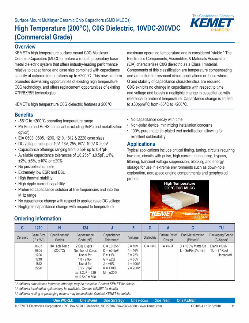
OverviewKEMET’s high temperature surface mount C0G Multilayer Ceramic Capacitors (MLCCs) feature a robust, proprietary base metal dielectric system that offers industry-leading performance relative to capacitance and case size combined with capacitance stability at extreme temperatures up to +200°C. This new platform promotes downsizing opportunities of existing high temperature C0G technology, and offers replacement opportunities of existing X7R/BX/BR technologies.
KEMET’s high temperature C0G dielectric features a 200°C
maximum operating temperature and is considered “stable.” The Electronics Components, Assemblies & Materials Association (EIA) characterizes C0G dielectric as a Class I material. Components of this classifi cation are temperature compensating and are suited for resonant circuit applications or those where Q and stability of capacitance characteristics are required. C0G exhibits no change in capacitance with respect to time and voltage and boasts a negligible change in capacitance with reference to ambient temperature. Capacitance change is limited to ±30ppm/ºC from -55°C to +200°C.
Surface Mount Multilayer Ceramic Chip Capacitors (SMD MLCCs)
High Temperature (200°C), C0G Dielectric, 10VDC-200VDC(Commercial Grade)
1 Additional capacitance tolerance offerings may be available. Contact KEMET for details. 2 Additional termination options may be available. Contact KEMET for details.3 Additional reeling or packaging options may be available. Contact KEMET for details.
Ordering InformationC 1210 H 124 J 5 G A C TU
Ceramic Case Size (L" x W")
Specifi cation/Series
Capacitance Code (pF)
Capacitance Tolerance1 Voltage Dielectric Failure Rate/
DesignEnd Metallization
(Plated)2
Packaging/Grade (C-Spec)3
060308051206121018122220
H= High Temp (200°C)
2 Sig. Digits + Number of Zeros
Use 9 for 1.0 - 9.9pFUse 8 for
0.5 - .99pFex. 2.2pF = 229ex. 0.5pF = 508
C = ±0.25pFD = ±0.5pFF = ±1%G = ±2%J = ±5%K = ±10%M = ±20%
8 = 10V4 = 16V3 = 25V5 = 50V1 = 100V2 = 200V
G = C0G A = N/A C = 100% Matte SnL = SnPb (5% min)
Blank = BulkTU = 7" Reel
Unmarked

© KEMET Electronics Corporation • P.O. Box 5928 • Greenville, SC 29606 (864) 963-6300 • www.kemet.com CC105-1 • 10/16/2010 12
Surface Mount Multilayer Ceramic Chip Capacitors – High Temperature
© KEMET Electronics Corporation • P.O. Box 5928 • Greenville, SC 29606 (864) 963-6300 • www.kemet.com C1001-1 • 10/19/2010 18
Surface Mount Multilayer Ceramic Chip Capacitors – High Temperature (200°C), C0G Dielectric, 10VDC-200VDC (Commercial Grade)
EIA Size Code
MetricSize Code L Length W Width B Bandwidth T Thickness Mounting
Technique0603 1608 1.60 (.063) ± 0.15 (.006) 0.80 (.032) ± 0.15 (.006) 0.35 (.014) ± 0.15 (.006)
See Table 2 for Thickness
Solder Wave or Solder Refl ow0805 2012 2.00 (.079) ± 0.20 (.008) 1.25 (.049) ± 0.20 (.008) 0.50 (0.02) ± 0.25 (.010)
1206 3216 3.20 (.126) ± 0.20 (.008) 1.60 (.063) ± 0.20 (.008) 0.50 (0.02) ± 0.25 (.010)1210 3225 3.20 (.126) ± 0.20 (.008) 2.50 (.098) ± 0.20 (.008) 0.50 (0.02) ± 0.25 (.010)
Solder Refl ow Only1812 4532 4.50 (.177) ± 0.30 (.012) 3.20 (.126) ± 0.30 (.012) 0.60 (.024) ± 0.35 (.014)
2220 5650 5.70 (.224) ± 0.40 (.016) 5.00 (.197) ± 0.40 (.016) 0.60 (.024) ± 0.35 (.014)
Dimensions – Millimeters (Inches)
Qualifi cation/Certifi cationCommercial grade products are subject to internal qualifi cation. Details regarding test methods and conditions are referenced in Table 4, Performance and Reliability.
Environmental ComplianceDevices with “C” end metallization option are RoHS PRC ( Peoples Republic of China) compliant. Devices with “L” end metallization option do no meet RoHS criteria.
Electrical Parameters/Characteristics
Item Parameters/CharacteristicsOperating Temperature Range: -55°C to +200°C
Capacitance Change with Reference to +25°C and 0 Vdc Applied (TCC): ±30PPM/ºC (up to 200ºC)
Aging Rate (Max % Cap Loss/Decade Hour): 0%
Dielectric Withstanding Voltage: 250% of rated voltage (5 ± 1 seconds and charge/discharge not exceeding 50mA)
Dissipation Factor (DF) Maximum Limits @ 25ºC: 0.1%
Insulation Resistance (IR) Limit @ 25°C: 1000 megohm microfarads or 100GΩ
Insulation Resistance (IR) Limit @ 200°C: 10 megohm microfarads or 1GΩ
To obtain IR limit, divide MΩ-µF value by the capacitance and compare to GΩ limit. Select the lower of the two limits.Capacitance and Dissipation Factor (DF) measured under the following conditions: 1kHz ± 50Hz and 1.0 ± 0.2 Vrms if capacitance ≤10µF 120Hz ± 10Hz and 0.5 ± 0.1 Vrms if capacitance >10µF
Cer
amic
Su
rfac
e M
ou
nt
W L
T B
S
100% Tin or SnPb Plate
Nickel Plate
Conductive MetalizationElectrodes

© KEMET Electronics Corporation • P.O. Box 5928 • Greenville, SC 29606 (864) 963-6300 • www.kemet.com CC105-1 • 10/16/2010 13
Surface Mount Multilayer Ceramic Chip Capacitors – High Temperature
© KEMET Electronics Corporation • P.O. Box 5928 • Greenville, SC 29606 (864) 963-6300 • www.kemet.com C1001-1 • 10/19/2010 19
Surface Mount Multilayer Ceramic Chip Capacitors – High Temperature (200°C), C0G Dielectric, 10VDC-200VDC (Commercial Grade)
Electrical Characteristics
Capacitance vs. Temperature with 25V DC Bias (Rated Voltage)
BME vs. PME/IR vs. Temperature with 25V DC Bias (Rated Voltage)IR vs. Temperature with 25V DC Bias (Rated Voltage)
DF vs. Temperature without DC Bias.
Delta Cap vs. Temperature (Typical) C1210H104J1GAC - Life Test IR Distribution (Lognormal)
0
50
100
150
200
-60
-40
-20
0 20 40 60 80 100
120
140
160
180
200
Cap
acita
nce
(nF)
Temperature (°C)
200ºC C0G 100nF no DC
200ºC C0G 100nF 25V DC
-1.00
-0.50
0.00
0.50
1.00
-60
-40
-20
0 20 40 60 80 100
120
140
160
180
200
DF
(%)
Temperature (°C)
200ºC C0G MLCC 100nF
-20
-15
-10
-5
0
5
10
15
20
-60
-40
-20
0 20 40 60 80 100
120
140
160
180
200
Del
ta C
ap (%
)
Temperature (ºC)
0 Vr
100% Vr
100.010.01.00.1
99
95908070605040302010
5
1
25°C IR (GOhms)
Per
cen
t
0 hrs2000 hrs
1.E+01
1.E+02
1.E+03
1.E+04
1.E+05
1.E+06
1.E+07
1.E+08
-60
-40
-20
0 20 40 60 80 100
120
140
160
180
200
IR (M
Ohm
s)
Temperature (°C)
PME C0G MLCC 1206/10nF
BME C0G MLCC 1206/10nF
1.E+00
1.E+01
1.E+02
1.E+03
1.E+04
1.E+05
1.E+06
1.E+07
1.E+08
-60
-40
-20
0 20 40 60 80 100
120
140
160
180
200
IR (M
Ohm
s)
Temperature (°C)
200ºC C0G MLCC 100nF
Electrical Characteristics – C0G Dielectric

© KEMET Electronics Corporation • P.O. Box 5928 • Greenville, SC 29606 (864) 963-6300 • www.kemet.com CC105-1 • 10/16/2010 14
Surface Mount Multilayer Ceramic Chip Capacitors – High Temperature
Cap Cap Code
Series C0603 C0805 C1206 C1210Voltage Code 8 4 3 5 1 2 8 4 3 5 1 2 8 4 3 5 1 2 8 4 3 5 1 2
Voltage DC 10 16 25 50 100
200 10 16 25 50 100
200 10 16 25 50 100
200 10 16 25 50 100
200
Cap Tolerance Product Availability and Chip Thickness Codes - See Table 2 for Chip Thickness Dimensions0.5-0.75 pF 508-759 C D CB CB CB CB CB CB DC DC DC DC DC DC1.0-2.4 pF 109-249 C D CB CB CB CB CB CB DC DC DC DC DC DC EB EB EB EB EB EB FB FB FB FB FB FB2.7-5.1 pF 279-519 C D K M CB CB CB CB CB CB DC DC DC DC DC DC EB EB EB EB EB EB FB FB FB FB FB FB5.6-9.1 pF 569-919 C D J K M CB CB CB CB CB CB DC DC DC DC DC DC EB EB EB EB EB EB FB FB FB FB FB FB10-13 pF 100-130 C D J K M CB CB CB CB CB CB DC DC DC DC DC DC EB EB EB EB EB EB FB FB FB FB FB FB15-24 pF 150-240 C D G J K M CB CB CB CB CB CB DC DC DC DC DC DC EB EB EB EB EB EB FB FB FB FB FB FB27-36 pF 270-360 D G J K M CB CB CB CB CB CB DC DC DC DC DC DC EB EB EB EB EB EB FB FB FB FB FB FB39-51 pF 390-510 D F G J K M CB CB CB CB CB CB DC DC DC DC DC DC EB EB EB EB EB EB FB FB FB FB FB FB56-91 pF 560-910 F G J K M CB CB CB CB CB CB DC DC DC DC DC DC EB EB EB EB EB EB FB FB FB FB FB FB
100-180 pF 101-181 F G J K M CB CB CB CB CB CB DC DC DC DC DC DC EB EB EB EB EB EB FB FB FB FB FB FB200 pF 201 F G J K M CB CB CB CB CB DC DC DC DC DC DC EB EB EB EB EB EB FB FB FB FB FB FB220 pF 221 F G J K M CB CB CB CB CB DC DC DC DC DC DC EB EB EB EB EB EB FB FB FB FB FB FB240 pF 241 F G J K M CB CB CB CB CB DC DC DC DC DC DC EB EB EB EB EB EB FB FB FB FB FB FB270 pF 271 F G J K M CB CB CB CB CB DC DC DC DC DC DC EB EB EB EB EB EB FB FB FB FB FB FB300 pF 301 F G J K M CB CB CB CB CB DC DC DC DC DC DC EB EB EB EB EB EB FB FB FB FB FB FB330 pF 331 F G J K M CB CB CB CB CB DC DC DC DC DC DC EB EB EB EB EB EB FB FB FB FB FB FB360 pF 361 F G J K M CB CB CB CB CB DC DC DC DC DC DC EB EB EB EB EB EB FB FB FB FB FB FB390 pF 391 F G J K M CB CB CB CB CB DC DC DC DC DC DC EB EB EB EB EB EB FB FB FB FB FB FB430 pF 431 F G J K M CB CB CB CB CB DC DC DC DC DC DC EB EB EB EB EB EB FB FB FB FB FB FB470 pF 471 F G J K M CB CB CB CB CB DC DC DC DC DC DD EB EB EB EB EB EB FB FB FB FB FB FB510 pF 511 F G J K M CB CB CB CB CB DC DC DC DC DC DC EB EB EB EB EB EB FB FB FB FB FB FB560 pF 561 F G J K M CB CB CB CB CB DC DC DC DC DC DC EB EB EB EB EB EB FB FB FB FB FB FB620 pF 621 F G J K M CB CB CB CB CB DC DC DC DC DC DC EB EB EB EB EB EC FB FB FB FB FB FB680 pF 681 F G J K M CB CB CB CB CB DC DC DC DC DC DC EB EB EB EB EB EC FB FB FB FB FB FB750 pF 751 F G J K M CB CB CB CB CB DC DC DC DC DC DC EB EB EB EB EB EC FB FB FB FB FB FB820 pF 821 F G J K M CB CB CB CB CB DC DC DC DC DC DC EB EB EB EB EB EC FB FB FB FB FB FB910 pF 911 F G J K M CB CB CB CB CB DC DC DC DC DD DD EB EB EB EB EB ED FB FB FB FB FB FB
1,000 pF 102 F G J K M CB CB CB CB CB DC DC DC DC DD DD EB EB EB EB EB EE FB FB FB FB FB FB1,100 pF 112 F G J K M CB CB CB CB CB DC DC DC DC DC EB EB EB EB EB EB FB FB FB FB FB FB1,200 pF 122 F G J K M CB CB CB CB CB DC DC DC DC DC EB EB EB EB EB EB FB FB FB FB FB FB1,300 pF 132 F G J K M CB CB CB CB CB DD DD DD DD DD EB EB EB EB EC EC FB FB FB FB FB FC1,500 pF 152 F G J K M CB CB CB CB CB DD DD DD DD DD EB EB EB EB ED EC FB FB FB FB FB FE1,600 pF 162 F G J K M CB CB CB CB CB DD DD DD DD DD EB EB EB EB ED ED FB FB FB FB FB FE1,800 pF 182 F G J K M CB CB CB CB CB DD DD DD DD DD EB EB EB EB ED ED FB FB FB FB FB FE2,000 pF 202 F G J K M CB CB CB CB CB DC DC DC DC DC EB EB EB EB ED ED FB FB FB FB FC FE2,200 pF 222 F G J K M CB CB CB CB CB DC DC DC DC DC EB EB EB EB EE EE FB FB FB FB FC FG2,400 pF 242 F G J K M CB CB CB CB CB DC DC DC DC DC EB EB EB EB EC EC FB FB FB FB FC FC2,700 pF 272 F G J K M CB CB CB CB CB DC DC DC DC DC EB EB EB EB EC EC FB FB FB FB FC FC3,000 pF 302 F G J K M CB CB CB CB CB DD DD DD DD DC EC EC EC EC EC FB FB FB FB FC FF3,300 pF 332 F G J K M CB CB CB CB CB DD DD DD DD DC EC EC EC EC EE FB FB FB FB FF FF3,600 pF 362 F G J K M CB CB CB CB CB DD DD DD DD DC EC EC EC EC EE FB FB FB FB FF FF3,900 pF 392 F G J K M CB CB CB CB CB DE DE DE DE DC EC EC EC EC EF FB FB FB FB FF FF4,300 pF 432 F G J K M CB CB CB CB CB DE DE DE DE DC EC EC EC EC EC FB FB FB FB FF FF4,700 pF 472 F G J K M CB CB CB CB CB DE DE DE DE DC EC EC EC EC EC FF FF FF FF FG FG5,100 pF 512 F G J K M CB CB CB CB DE DE DE DE DC ED ED ED ED ED FB FB FB FB FG FG5,600 pF 562 F G J K M CB CB CB CB DC DC DC DC DC ED ED ED ED ED FB FB FB FB FG FG6,200 pF 622 F G J K M CB CB CB CB DC DC DC DC DC EB EB EB EB EB FB FB FB FB FG6,800 pF 682 F G J K M CB CB CB CB DC DC DC DC DC EB EB EB EB EB FB FB FB FB FG7,500 pF 752 F G J K M CB CB CB DC DC DC DC DC EB EB EB EB EB FC FC FC FC FC8,200 pF 822 F G J K M CB CB CB DC DC DC DC DC EC EC EC EC EB FC FC FC FC FC9,100 pF 912 F G J K M CB CB CB DC DC DC DC DC EC EC EC EC EB FE FE FE FE FE
10,000 pF 103 F G J K M CB CB CB DC DC DC DC DD ED ED ED ED EB FF FF FF FF FF12,000 pF 123 F G J K M DC DC DC DC DE EB EB EB EB EB FG FG FG FG FB15,000 pF 153 F G J K M DC DC DC DD DG EB EB EB EB EB FG FG FG FG FB18,000 pF 183 F G J K M DC DC DC DD EB EB EB EB EB FB FB FB FB FB22,000 pF 223 F G J K M DD DD DD DF EB EB EB EB EC FB FB FB FB FB27,000 pF 273 F G J K M DF DF DF EB EB EB EB EE FB FB FB FB FB
Cap Cap Code
Voltage DC 10 16 25 50 100
200 10 16 25 50 100
200 10 16 25 50 100
200 10 16 25 50 100
200
Voltage Code 8 4 3 5 1 2 8 4 3 5 1 2 8 4 3 5 1 2 8 4 3 5 1 2
Series C0603 C0805 C1206 C1210
Table 1A – C0G Dielectric (0603 - 1210 Case Sizes)
UD = Under Developement

© KEMET Electronics Corporation • P.O. Box 5928 • Greenville, SC 29606 (864) 963-6300 • www.kemet.com CC105-1 • 10/16/2010 15
Surface Mount Multilayer Ceramic Chip Capacitors – High Temperature
Cap Cap Code
Series C1812 C2220Voltage Code 1 2 5 1
Voltage DC 100 200 50 100Cap Tolerance See Table 2 for Chip Thickness Dimensions
15,000 pF 153 F G J K M GB GB18,000 pF 183 F G J K M GB GB22,000 pF 223 F G J K M GB GB27,000 pF 273 F G J K M GB GB33,000 pF 333 F G J K M GB GB47,000 pF 473 F G J K M GB GB56,000 pF 563 F G J K M GB GB68,000 pF 683 F G J K M GB GB82,000 pF 823 F G J K M GB GB
0.10 uF 104 F G J K M GB GD0.12 uF 124 F G J K M GB GH0.15 uF 154 F G J K M GD GN0.18 uF 184 F G J K M GH0.22 uF 224 F G J K M GK0.27 uF 274 F G J K M0.33 uF 334 F G J K M0.47 uF 474 F G J K M JO0.56 uF 564 F G J K M0.68 uF 684 F G J K M0.82 uF 824 F G J K M
Cap CapCode
Voltage DC 100 200 50 100Voltage Code 1 2 5 1
Series C1812 C2220
Table 1A – C0G Dielectric (0603 - 1210 Case Sizes) con't
Table 1B – (1812 - 2220 Case Sizes)
Cap Cap Code
Series C0603 C0805 C1206 C1210Voltage Code 8 4 3 5 1 2 8 4 3 5 1 2 8 4 3 5 1 2 8 4 3 5 1 2
Voltage DC 10 16 25 50 100
200 10 16 25 50 100
200 10 16 25 50 100
200 10 16 25 50 100
200
Cap Tolerance Product Availability and Chip Thickness Codes - See Table 2 for Chip Thickness Dimensions33,000 pF 333 F G J K M DG DG DG EB EB EB EB EE FB FB FB FB FB47,000 pF 473 F G J K M UD UD UD EC EC EC EE EH FB FB FB FB FE56,000 pF 563 F G J K M ED ED ED EF FB FB FB FB FF68,000 pF 683 F G J K M EF EF EF EH FB FB FB FC FG82,000 pF 823 F G J K M EH EH EH EH FC FC FC FF FH
0.10 uF 104 F G J K M EH EH EH FE FE FE FG FM0.12 uF 124 F G J K M FG FG FG FH0.15 uF 154 F G J K M FH FH FH FM0.18 uF 184 F G J K M UD UD UD0.22 uF 224 F G J K M UD UD UD
Cap Cap Code
Voltage DC 10 16 25 50 100
200 10 16 25 50 100
200 10 16 25 50 100
200 10 16 25 50 100
200
Voltage Code 8 4 3 5 1 2 8 4 3 5 1 2 8 4 3 5 1 2 8 4 3 5 1 2
Series C0603 C0805 C1206 C1210
UD = Under Developement
© KEMET Electronics Corporation • P.O. Box 5928 • Greenville, SC 29606 (864) 963-6300 • www.kemet.com CC105-1 • 10/16/2010 16
Surface Mount Multilayer Ceramic Chip Capacitors – High Temperature
© KEMET Electronics Corporation • P.O. Box 5928 • Greenville, SC 29606 (864) 963-6300 • www.kemet.com C1001-1 • 10/19/2010 24
Surface Mount Multilayer Ceramic Chip Capacitors – High Temperature (200°C), C0G Dielectric, 10VDC-200VDC (Commercial Grade)
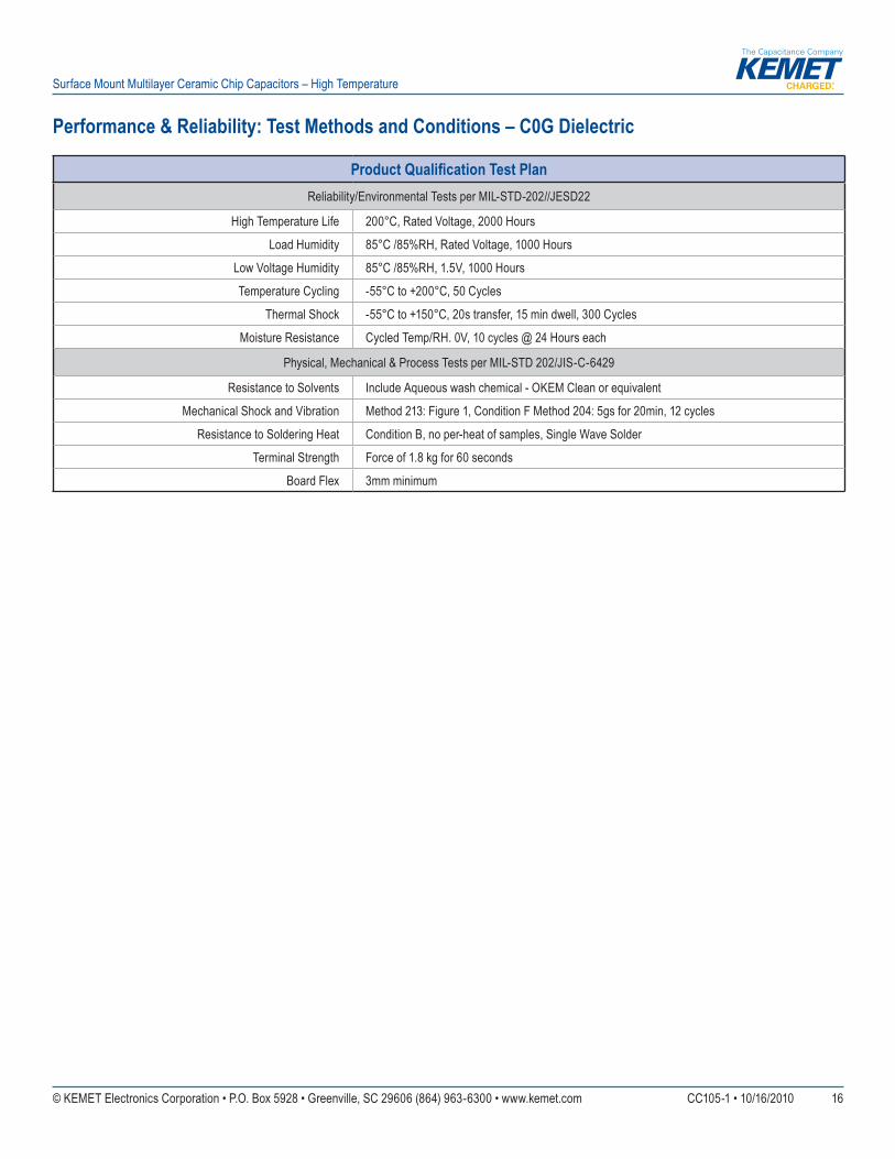
Table 4 – Performance & Reliability: Test Methods and Conditions
Product Qualifi cation Test PlanReliability/Environmental Tests per MIL-STD-202//JESD22
High Temperature Life 200°C, Rated Voltage, 2000 Hours
Load Humidity 85°C /85%RH, Rated Voltage, 1000 Hours
Low Voltage Humidity 85°C /85%RH, 1.5V, 1000 Hours
Temperature Cycling -55°C to +200°C, 50 Cycles
Thermal Shock -55°C to +150°C, 20s transfer, 15 min dwell, 300 Cycles
Moisture Resistance Cycled Temp/RH. 0V, 10 cycles @ 24 Hours each
Physical, Mechanical & Process Tests per MIL-STD 202/JIS-C-6429
Resistance to Solvents Include Aqueous wash chemical - OKEM Clean or equivalent
Mechanical Shock and Vibration Method 213: Figure 1, Condition F Method 204: 5gs for 20min, 12 cycles
Resistance to Soldering Heat Condition B, no per-heat of samples, Single Wave Solder
Terminal Strength Force of 1.8 kg for 60 seconds
Board Flex 3mm minimum
Performance & Reliability: Test Methods and Conditions – C0G Dielectric

© KEMET Electronics Corporation • P.O. Box 5928 • Greenville, SC 29606 (864) 963-6300 • www.kemet.com CC105-1 • 10/16/2010 17
Surface Mount Multilayer Ceramic Chip Capacitors – High Temperature
Table 2 – Chip Thickness / Packaging QuantitiesThickness
Code Chip Size
Thickness ± Range (mm)
Qty per Reel 7" Plastic
Qty per Reel 13" Plastic
Qty per Reel 7" Paper
Qty per Reel 13" Paper
Qty per Bulk Cassette
AA 01005 0.20 ± 0.02 15000AB 0201 0.30 ± 0.03 15000BB 0402 0.50 ± 0.05 10000 50000 50000CB 0603 0.80 ± 0.07 4000 10000 15000CC 0603 0.80 ± 0.10 4000 10000CD 0603 0.80 ± 0.15 4000 10000DC 0805 0.78 ± 0.10 4000 10000DD 0805 0.90 ± 0.10 4000 10000DL 0805 0.95 ± 0.10 4000 10000DE 0805 1.00 ± 0.10 2500 10000DF 0805 1.10 ± 0.10 2500 10000DG 0805 1.25 ± 0.15 2500 10000DH 0805 1.25 ± 0.20 2500 10000EB 1206 0.78 ± 0.10 4000 10000 4000 10000EK 1206 0.80 ± 0.10 2000 8000EC 1206 0.90 ± 0.10 4000 10000EN 1206 0.95 ± 0.10 4000 10000ED 1206 1.00 ± 0.10 2500 10000EE 1206 1.10 ± 0.10 2500 10000EF 1206 1.20 ± 0.15 2500 10000EM 1206 1.25 ± 0.15 2500 10000EG 1206 1.60 ± 0.15 2000 8000EH 1206 1.60 ± 0.20 2000 8000EJ 1206 1.70 ± 0.20 2000 8000FB 1210 0.78 ± 0.10 4000 10000FC 1210 0.90 ± 0.10 4000 10000FD 1210 0.95 ± 0.10 4000 10000FE 1210 1.00 ± 0.10 2500 10000FF 1210 1.10 ± 0.10 2500 10000FG 1210 1.25 ± 0.15 2500 10000FL 1210 1.40 ± 0.15 2000 8000FO 1210 1.50 ± 0.20 2000 8000FH 1210 1.55 ± 0.15 2000 8000FP 1210 1.60 ± 0.20 2000 8000FM 1210 1.70 ± 0.20 2000 8000FJ 1210 1.85 ± 0.20 2000 8000FN 1210 1.85 ± 0.20 2000 8000FT 1210 1.90 ± 0.20 1500 4000FK 1210 2.10 ± 0.20 2000 8000FR 1210 2.25 ± 0.20 2000 8000FS 1210 2.50 ± 0.20 1000 4000PA 1220 0.80 ± 0.10 4000 10000MA 1632 0.80 ± 0.10 4000 10000NA 1706 0.90 ± 0.10 4000 10000NA 1706 0.90 ± 0.10 4000 10000LD 1808 0.90 ± 0.10 2500 10000LA 1808 1.40 ± 0.15 1000 4000LB 1808 1.60 ± 0.15 1000 4000LC 1808 2.00 ± 0.15 1000 4000GB 1812 1.00 ± 0.10 1000 4000GC 1812 1.10 ± 0.10 1000 4000GD 1812 1.25 ± 0.15 1000 4000GE 1812 1.30 ± 0.10 1000 4000GH 1812 1.40 ± 0.15 1000 4000GF 1812 1.50 ± 0.10 1000 4000GG 1812 1.55 ± 0.10 1000 4000GK 1812 1.60 ± 0.20 1000 4000GJ 1812 1.70 ± 0.15 1000 4000GN 1812 1.70 ± 0.20 1000 4000GL 1812 1.90 ± 0.20 1000 4000GM 1812 2.00 ± 0.20 1000 4000GO 1812 2.50 ± 0.20 500 2000HB 1825 1.10 ± 0.15 1000 4000HC 1825 1.15 ± 0.15 1000 4000HD 1825 1.30 ± 0.15 1000 4000HE 1825 1.40 ± 0.15 1000 4000HF 1825 1.50 ± 0.15 1000 4000HG 1825 1.60 ± 0.20 1000 4000JB 2220 1.00 ± 0.15 1000 4000JC 2220 1.10 ± 0.15 1000 4000JD 2220 1.30 ± 0.15 1000 4000JE 2220 1.40 ± 0.15 1000 4000JF 2220 1.50 ± 0.15 1000 4000JP 2220 1.60 ± 0.20 1000 4000JG 2220 1.70 ± 0.15 1000 4000JH 2220 1.80 ± 0.15 1000 4000JO 2220 2.40 ± 0.15 500 2000KB 2225 1.00 ± 0.15 1000 4000KC 2225 1.10 ± 0.15 1000 4000KD 2225 1.30 ± 0.15 1000 4000KE 2225 1.40 ± 0.15 1000 4000KF 2225 1.60 ± 0.20 1000 4000
Package Quantity Based on Finished Chip Thickness Specifications
© KEMET Electronics Corporation • P.O. Box 5928 • Greenville, SC 29606 (864) 963-6300 • www.kemet.com CC105-1 • 10/16/2010 18
Surface Mount Multilayer Ceramic Chip Capacitors – High Temperature
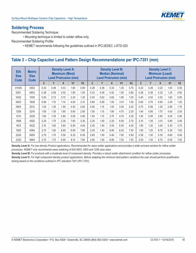
Soldering Process Recommended Soldering Technique: • Mounting technique is limited to solder reflow only.Recommended Soldering Profile: • KEMET recommends following the guidelines outlined in IPC/JEDEC J-STD-020
Table 3 – Chip Capacitor Land Pattern Design Recommendations per IPC-7351 (mm)
EIA Size Code
Metric Size Code
Density Level A: Maximum (Most)
Land Protrusion (mm)
Density Level B: Median (Nominal)
Land Protrusion (mm)
Density Level C: Minimum (Least)
Land Protrusion (mm)C Y X V1 V2 C Y X V1 V2 C Y X V1 V2
01005 0402 0.33 0.46 0.43 1.60 0.90 0.28 0.36 0.33 1.30 0.70 0.23 0.26 0.23 1.00 0.500201 0603 0.38 0.56 0.52 1.80 1.00 0.33 0.46 0.42 1.50 0.80 0.28 0.36 0.32 1.20 0.600402 1005 0.50 0.72 0.72 2.20 1.20 0.45 0.62 0.62 1.90 1.00 0.40 0.52 0.52 1.60 0.800603 1608 0.90 1.15 1.10 4.00 2.10 0.80 0.95 1.00 3.10 1.50 0.60 0.75 0.90 2.40 1.200805 2012 1.00 1.35 1.55 4.40 2.60 0.90 1.15 1.45 3.50 2.00 0.75 0.95 1.35 2.80 1.701206 3216 1.60 1.35 1.90 5.60 2.90 1.50 1.15 1.80 4.70 2.30 1.40 0.95 1.70 4.00 2.001210 3225 1.60 1.35 2.80 5.65 3.80 1.50 1.15 2.70 4.70 3.20 1.40 0.95 2.60 4.00 2.901808 4520 2.30 1.75 2.30 7.40 3.30 2.20 1.55 2.20 6.50 2.70 2.10 1.35 2.10 5.80 2.401812 4532 2.15 1.60 3.60 6.90 4.60 2.05 1.40 3.50 6.00 4.00 1.95 1.20 3.40 5.30 3.701825 4564 2.15 1.60 6.90 6.90 7.90 2.05 1.40 6.80 6.00 7.30 1.95 1.20 6.70 5.30 7.002220 5650 2.75 1.70 5.50 8.20 6.50 2.65 1.50 5.40 7.30 5.90 2.55 1.30 5.30 6.60 5.602225 5664 2.70 1.70 6.90 8.10 7.90 2.60 1.50 6.80 7.20 7.30 2.50 1.30 6.70 6.50 7.00
Density Level A: For low-density Product applications. Recommended for wave solder applications and provides a wider process window for reflow solder processes. KEMET only recommends wave soldering of EIA 0603, 0805 and 1206 case sizes.Density Level B: For products with a moderate level of component density. Provides a robust solder attachment condition for reflow solder processes.Density Level C: For high component density product applications. Before adapting the minimum land pattern variations the user should perform qualification testing based on the conditions outlined in IPC standard 7351 (IPC-7351).
© KEMET Electronics Corporation • P.O. Box 5928 • Greenville, SC 29606 (864) 963-6300 • www.kemet.com CC105-1 • 10/16/2010 19
Surface Mount Multilayer Ceramic Chip Capacitors – High Temperature
Tape & Reel Packaging InformationKEMET offers Multilayer Ceramic Chip Capacitors packaged in 8mm, 12mm and 16mm tape on 7" and 13" reels in accordance with EIA standard 481. This packaging system is compatible with all tape fed automatic pick and place systems. See Table 2 for details on reeling quantities for commercial chips.
Table 5 – Carrier Tape Confi guration (mm)
EIA Case Size Tape size (W)* Pitch (P1)*
01005 - 0402 8 2
0603 - 1210 8 4
1805 - 1808 12 4
≥ 1812 12 8
KPS 1210 12 8
KPS 1812 & 2220 16 12
Array 0508 & 0612 8 4
*Refer to Figure 1 for W and P1 carrier tape reference locations.*Refer to Table 6 for tolerance specifi cations.
8mm, 12mmor 16mm Carrier Tape
178mm (7.00")or
330mm (13.00")
Anti-Static Reel
Embossed Plastic* or Punched Paper Carrier.
Embossment or Punched Cavity
Anti-Static Cover Tape(.10mm (.004") Max Thickness)
Chip and KPS Orientation in Pocket(except 1825 Commercial, and 1825 & 2225 Military)
*EIA 01005, 0201, 0402 and 0603 case sizes available on punched paper carrier only.
KEMET®
Bar Code Label
Sprocket Holes

© KEMET Electronics Corporation • P.O. Box 5928 • Greenville, SC 29606 (864) 963-6300 • www.kemet.com CC105-1 • 10/16/2010 20
Surface Mount Multilayer Ceramic Chip Capacitors – High Temperature
Figure 1 – Embossed (Plastic) Carrier Tape Dimensions
Table 6 – Embossed (Plastic) Carrier Tape DimensionsMetric will govern
Constant Dimensions — Millimeters (Inches)
Tape Size D0 D1 Min. Note 1 E1 P0 P2
R Ref. Note 2
S1 Min.Note 3 T Max. T1 Max.
8mm
1.5 +0.10/-0.0 (0.059 +0.004/-0.0)
1.0 (0.039)
1.75 ± 0.10 (0.069 ± 0.004)
4.0 ± 0.10 (0.157 ± 0.004)
2.0 ± 0.05 (0.079 ± 0.002)
25.0 (0.984)
0.600 (0.024)
0.600 (0.024)
0.100 (0.004)12mm 1.5
(0.059)30
(1.181)16mm
Variable Dimensions — Millimeters (Inches)
Tape Size Pitch B1 Max. Note 4 E2 Min. F P1 T2 Max W Max A0,B0 & K0
8mm Single (4mm) 4.35 (0.171)
6.25 (0.246)
3.5 ± 0.05 (0.138 ± 0.002)
4.0 ± 0.10 (0.157 ± 0.004)
2.5 (0.098)
8.3 (0.327)
Note 512mm Single (4mm) & Double (8mm)
8.2 (0.323)
10.25 (0.404)
5.5 ± 0.05 (0.217 ± 0.002)
8.0 ± 0.10 (0.315 ± 0.004)
4.6 (0.181)
12.3 (0.484)
16mm Triple (12mm) 12.1 (0.476)
14.25 (0.561)
5.5 ± 0.05 (0.217 ± 0.002)
8.0 ± 0.10 (0.315 ± 0.004)
4.6 (0.181)
16.3 (0.642)
1. The embossment hole location shall be measured from the sprocket hole controlling the location of the embossment. Dimensions of embossment location and hole location shall be applied independent of each other.
2. The tape with or without components shall pass around R without damage (see Figure 5).3. If S1<1.0 mm, there may not be enough area for cover tape to be properly applied (see EIA Document 481 paragraph 4.3 (b)).4. B1 dimension is a reference dimension for tape feeder clearance only.5. The cavity defi ned by A0, B0 and K0 shall surround the component with suffi cient clearance that: (a) the component does not protrude above the top surface of the carrier tape. (b) the component can be removed from the cavity in a vertical direction without mechanical restriction, after the top cover tape has been removed. (c) rotation of the component is limited to 20° maximum for 8 and 12mm tapes and 10° maximum for 16mm tapes (see Figure 3). (d) lateral movement of the component is restricted to 0.5 mm maximum for 8mm and 12mm wide tape and to 1.0mm maximum for 16mm tape (see Figure 4). (e) for KPS Series product A0 and B0 are measured on a plane 0.3mm above the bottom of the pocket. (f) see Addendum in EIA Document 481 for standards relating to more precise taping requirements.
PoT
F
W
Center Lines of Cavity
Ao
Bo
User Direction of Unreeling
Cover Tape
Ko
B1 is for tape feeder reference only, including draft concentric about B o.
T2
ØD1
ØDo
B1
S1
T1
E1
E2
P1
P2
EmbossmentFor cavity size,see Note 1 Table 5
[10 pitches cumulativetolerance on tape ±0.2 mm]

© KEMET Electronics Corporation • P.O. Box 5928 • Greenville, SC 29606 (864) 963-6300 • www.kemet.com CC105-1 • 10/16/2010 21
Surface Mount Multilayer Ceramic Chip Capacitors – High Temperature
Figure 2 – Punched (Paper) Carrier Tape Dimensions
User Direction of Unreeling
Top Cover Tape
T
Center Lines of Cavity
P1
ØDo PoP2
E1
F
E2W
G
A0
B0
Cavity Size,SeeNote 1, Table 7
Bottom Cover Tape
T1
T1
Bottom Cover Tape
[10 pitches cumulativetolerance on tape ±0.2 mm]
Table 7 – Punched (Paper) Carrier Tape Dimensions Metric will govern
Constant Dimensions — Millimeters (Inches)Tape Size D0 E1 P0 P2 T1Max G Min R Ref.
Note 2
8mm 1.5 +0.10-0.0 (0.059 +0.004, -0.0)
1.75 ±0.10 (0.069 ±0.004)
4.0 ±0.10 (0.157 ±0.004)
2.0 ±0.05 (0.079 ±0.002)
0.10 (.004) Max.
0.75 (.030)
25 (.984)
Variable Dimensions — Millimeters (Inches)Tape Size Pitch E2 Min F P1 T Max W Max A0 B0
8mm Half (2mm) 6.25 (0.246)
3.5 ± 0.05 (0.138 ± 0.002)
2.0 ± 0.05 (0.079 ± 0.002) 1.1
(0.098)
8.3 (0.327) Note 5
8mm Single (4mm) 4.0 ± 0.10 (0.157 ± 0.004)
8.3 (0.327)
1. The cavity defi ned by A0, B0 and T shall surround the component with suffi cient clearance that: a) the component does not protrude beyond either surface of the carrier tape. b) the component can be removed from the cavity in a vertical direction without mechanical restriction, after the top cover tape has been removed. d) lateral movement of the component is restricted to 0.5 mm maximum (see Figure 4). e) see Addendum in EIA Document 481 for standards relating to more precise taping requirements.2. The tape with or without components shall pass around R without damage (see Figure 5).

© KEMET Electronics Corporation • P.O. Box 5928 • Greenville, SC 29606 (864) 963-6300 • www.kemet.com CC105-1 • 10/16/2010 22
Surface Mount Multilayer Ceramic Chip Capacitors – High Temperature
Packaging Information Performance Notes1. Cover Tape Break Force: 1.0 Kg Minimum.2. Cover Tape Peel Strength: The total peel strength of the cover tape from the carrier tape shall be:
The direction of the pull shall be opposite the direction of the carrier tape travel. The pull angle of the carrier tape shall be 165° to 180° from the plane of the carrier tape. During peeling, the carrier and/or cover tape shall be pulled at a velocity of 300±10 mm/minute.
3. Labeling: Bar code labeling (standard or custom) shall be on the side of the reel opposite the sprocket holes. Refer to EIA-556 and EIA-624.
Figure 3 – Maximum Component Rotation
Ao
Bo
°T
°s
Maximum Component RotationTop View
Maximum Component RotationSide View
Tape MaximumWidth (mm) Rotation ( °
T)8,12 20 16-200 10 Tape Maximum
Width (mm) Rotation ( °S)
8,12 20 16-56 1072-200 5
Typical Pocket Centerline
Typical Component Centerline
Figure 4 – Maximum Lateral Movement
0.5 mm maximum0.5 mm maximum
8mm & 12mm Tape
1.0 mm maximum1.0 mm maximum
16mm Tape
Figure 5 – Bending Radius
RRBending
Radius
EmbossedCarrier
PunchedCarrier
Tape Width Peel Strength8mm 0.1 Newton to 1.0 Newton (10gf to 100gf)
12mm & 16mm 0.1 Newton to 1.3 Newton (10gf to 130gf)

© KEMET Electronics Corporation • P.O. Box 5928 • Greenville, SC 29606 (864) 963-6300 • www.kemet.com CC105-1 • 10/16/2010 23
Surface Mount Multilayer Ceramic Chip Capacitors – High Temperature
Figure 6 – Reel Dimensions
Table 8 – Reel DimensionsMetric will govern
Constant Dimensions — Millimeters (Inches)
Tape Size A B Min C D Min
8mm 178 ± 0.20 (7.008 ± 0.008)
or330 ± 0.20
(13.000 ± 0.008)
1.5 (0.059)
13.0 +0.5/-0.2 (0.521 +0.02/-0.008)
20.2 (0.795)12mm
16mm
Variable Dimensions — Millimeters (Inches)
Tape Size N Min W1 W2 Max W3
8mm 50
(1.969)
8.4 +1.5/-0.0(0.331 +0.059/-0.0)
14.4 (0.567)
Shall accommodate tape width without interference12mm 12.4 +2.0/-0.0
(0.488 +0.078/-0.0) 18.4
(0.724)16mm 16.4 +2.0/-0.0
(0.646 +0.078/-0.0)22.4
(0.882)
A D (See Note)
Full Radius,See Note
B (see Note)
Access Hole atSlot Location(Ø 40 mm min.)
If present,tape slot in corefor tape start:2.5 mm min. width x10.0 mm min. depth
W3 (Includes flange distortion at outer edge)
W2 (Measured at hub)
W1 (Measured at hub)
C(Arbor holediameter)
Note: Drive spokes optional; if used, dimensions B and D shall apply.
N

© KEMET Electronics Corporation • P.O. Box 5928 • Greenville, SC 29606 (864) 963-6300 • www.kemet.com CC105-1 • 10/16/2010 24
Surface Mount Multilayer Ceramic Chip Capacitors – High Temperature
Figure 7 – Tape Leader & Trailer Dimensions
Trailer160 mm minimum,
Carrier Tape
END STARTRound Sprocket Holes
Elongated Sprocket Holes(32 mm tape and wider)
Top Cover Tape
Top Cover Tape
Punched Carrier8 mm & 12 mm only
Embossed Carrier
Components
100 mm Min.Leader
400 mm Minimum,
Figure 8 – Maximum CamberCarrier Tape
Round Sprocket Holes
1 mm maximum, either direction
Straight Edge
250 mm
Elongated sprocket holes(32 mm & wider tapes)
© KEMET Electronics Corporation • P.O. Box 5928 • Greenville, SC 29606 (864) 963-6300 • www.kemet.com CC105-1 • 10/16/2010 25
Surface Mount Multilayer Ceramic Chip Capacitors – High Temperature
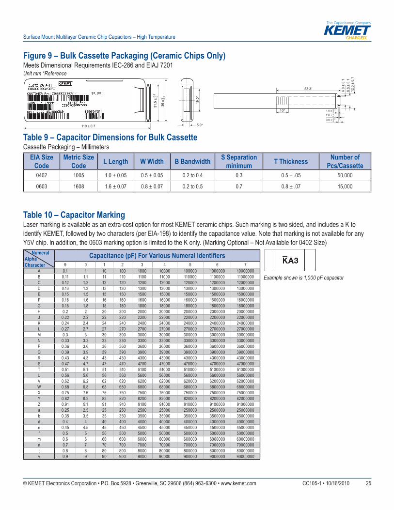
Figure 9 – Bulk Cassette Packaging (Ceramic Chips Only)Meets Dimensional Requirements IEC-286 and EIAJ 7201Unit mm *Reference
Table 9 – Capacitor Dimensions for Bulk CassetteCassette Packaging – Millimeters
Table 10 – Capacitor MarkingLaser marking is available as an extra-cost option for most KEMET ceramic chips. Such marking is two sided, and includes a K to identify KEMET, followed by two characters (per EIA-198) to identify the capacitance value. Note that marking is not available for any Y5V chip. ln addition, the 0603 marking option is limited to the K only. (Marking Optional – Not Available for 0402 Size)
Example shown is 1,000 pF capacitor
EIA Size Code
Metric Size Code L Length W Width B Bandwidth S Separation
minimum T Thickness Number of Pcs/Cassette
0402 1005 1.0 ± 0.05 0.5 ± 0.05 0.2 to 0.4 0.3 0.5 ± .05 50,000
0603 1608 1.6 ± 0.07 0.8 ± 0.07 0.2 to 0.5 0.7 0.8 ± .07 15,000
110 ± 0.7
31.5
± 00.
2
36 ±
0 0.2
19.0
*
5 0*
10*
53 3* 68
± 0.
18
8 ±
0.1
12.0
± 0
.1
3.0 ± 00.2
2.0 ± 0.10
1.5 ± 00.1
Numeral Alpha Character
Capacitance (pF) For Various Numeral Identifiers9 0 1 2 3 4 5 6 7
A 0.1 1 10 100 1000 10000 100000 1000000 10000000B 0.11 1.1 11 110 1100 11000 110000 1100000 11000000C 0.12 1.2 12 120 1200 12000 120000 1200000 12000000D 0.13 1.3 13 130 1300 13000 130000 1300000 13000000E 0.15 1.5 15 150 1500 15000 150000 1500000 15000000F 0.16 1.6 16 160 1600 16000 160000 1600000 16000000G 0.18 1.8 18 180 1800 18000 180000 1800000 18000000H 0.2 2 20 200 2000 20000 200000 2000000 20000000J 0.22 2.2 22 220 2200 22000 220000 2200000 22000000K 0.24 2.4 24 240 2400 24000 240000 2400000 24000000L 0.27 2.7 27 270 2700 27000 270000 2700000 27000000M 0.3 3 30 300 3000 30000 300000 3000000 30000000N 0.33 3.3 33 330 3300 33000 330000 3300000 33000000P 0.36 3.6 36 360 3600 36000 360000 3600000 36000000Q 0.39 3.9 39 390 3900 39000 390000 3900000 39000000R 0.43 4.3 43 430 4300 43000 430000 4300000 43000000S 0.47 4.7 47 470 4700 47000 470000 4700000 47000000T 0.51 5.1 51 510 5100 51000 510000 5100000 51000000U 0.56 5.6 56 560 5600 56000 560000 5600000 56000000V 0.62 6.2 62 620 6200 62000 620000 6200000 62000000W 0.68 6.8 68 680 6800 68000 680000 6800000 68000000X 0.75 7.5 75 750 7500 75000 750000 7500000 75000000Y 0.82 8.2 82 820 8200 82000 820000 8200000 82000000Z 0.91 9.1 91 910 9100 91000 910000 9100000 91000000a 0.25 2.5 25 250 2500 25000 250000 2500000 25000000b 0.35 3.5 35 350 3500 35000 350000 3500000 35000000d 0.4 4 40 400 4000 40000 400000 4000000 40000000e 0.45 4.5 45 450 4500 45000 450000 4500000 45000000f 0.5 5 50 500 5000 50000 500000 5000000 50000000m 0.6 6 60 600 6000 60000 600000 6000000 60000000n 0.7 7 70 700 7000 70000 700000 7000000 70000000t 0.8 8 80 800 8000 80000 800000 8000000 80000000y 0.9 9 90 900 9000 90000 900000 9000000 90000000

© KEMET Electronics Corporation • P.O. Box 5928 • Greenville, SC 29606 (864) 963-6300 • www.kemet.com CC105-1 • 10/16/2010 26
Surface Mount Multilayer Ceramic Chip Capacitors – High Temperature
Other KEMET Resources
DisclaimerAll product specifi cations, statements, information and data (collectively, the “Information”) are subject to change without notice.
All Information given herein is believed to be accurate and reliable, but is presented without guarantee, warranty, or responsibility of any kind, expressed or implied.
Statements of suitability for certain applications are based on our knowledge of typical operating conditions for such applications, but are not intended to constitute – and we specifi cally disclaim – any warranty concerning suitability for a specifi c customer application or use. This Information is intended for use only by customers who have the requisite experience and capability to determine the correct products for their application. Any technical advice inferred from this Information or otherwise provided by us with reference to the use of our products is given gratis, and we assume no obligation or liability for the advice given or results obtained.
Although we design and manufacture our products to the most stringent quality and safety standards, given the current state of the art, isolated component failures may still occur. Accordingly, customer applications which require a high degree of reliability or safety should employ suitable designs or other safeguards (such as installation of protective circuitry or redundancies) in order to ensure that the failure of an electrical component does not result in a risk of personal injury or property damage.
Although all product-related warnings, cautions and notes must be observed, the customer should not assume that all safety measures are indicated or that other measures may not be required.
ToolsResource Location
Confi gure A Part: CapEdge http://capacitoredge.kemet.comSPICE & FIT Software http://www.kemet.com/spice
Search Our FAQs: KnowledgeEdge http://www.kemet.com/keask
Product InformationResource Location
Products http://www.kemet.com/productsTechnical Resources (Including Soldering
Techniques) http://www.kemet.com/technicalpapers
RoHS Statement http://www.kemet.com/rohsQuality Documents http://www.kemet.com/qualitydocuments
Product RequestResource Location
Sample Request http://www.kemet.com/sampleEngineering Kit Request http://www.kemet.com/kits
ContactResource Location
Website www.kemet.comContact Us http://www.kemet.com/contact
Investor Relations http://www.kemet.com/irCall Us 1-877-MyKEMETTwitter http://twitter.com/kemetcapacitors

© KEMET Electronics Corporation • P.O. Box 5928 • Greenville, SC 29606 (864) 963-6300 • www.kemet.com CC105-1 • 10/16/2010 27
Surface Mount Multilayer Ceramic Chip Capacitors – High Temperature
KEMET Corporation World Headquarters2835 KEMET WaySimpsonville, SC 29681
Mailing Address:P.O. Box 5928 Greenville, SC 29606
www.kemet.com Tel: 864-963-6300 Fax: 864-963-6521
Corporate Offi cesFort Lauderdale, FLTel: 954-766-2800
North America SoutheastLake Mary, FLTel: 407-855-8886
NortheastWilmington, MATel: 978-658-1663
West Chester, PATel: 610-692-4642
CentralSchaumburg, IL Tel: 847-882-3590
Carmel, INTel: 317-706-6742
WestMilpitas, CATel: 408-433-9950
Mexico Zapopan, Jalisco Tel: 52-33-3123-2141
Europe
Southern EuropeGeneva, SwitzerlandTel: 41-22-715-0100
Paris, FranceTel: 33-1-4646-1009
Sasso Marconi, ItalyTel: 39-051-939111
Milan, ItalyTel: 39-02-57518176
Rome, ItalyTel: 39-06-23231718
Madrid, SpainTel: 34-91-804-4303
Central EuropeLandsberg, Germany Tel: 49-8191-3350800
Dortmund, GermanyTel: 49-2307-3619672
Kwidzyn, PolandTel: 48-55-279-7025
Northern EuropeBishop’s Stortford, United Kingdom Tel: 44-1279-757201
Weymouth, United KingdomTel: 44-1305-830747
Coatbridge, ScotlandTel: 44-1236-434455
Färjestaden, SwedenTel: 46-485-563934
Espoo, FinlandTel: 358-9-5406-5000
Asia
Northeast AsiaHong KongTel: 852-2305-1168
Shenzhen, ChinaTel: 86-755-2518-1306
Beijing, ChinaTel: 86-10-5829-1711
Shanghai, ChinaTel: 86-21-6447-0707
Taipei, TaiwanTel: 886-2-27528585
Southeast AsiaSingaporeTel: 65-6586-1900
Penang, MalaysiaTel: 60-4-6430200
Bangalore, IndiaTel: 91-806-53-76817
Note: KEMET reserves the right to modify minor details of internal and external construction at any time in the interest of product improvement. KEMET does not assume any responsibility for infringement that might result from the use of KEMET Capacitors in potential circuit designs. KEMET is a registered trademark of KEMET Electronics Corporation.