
The Neuroscience of Language. on Brain Circuits of Words and Serial Order by Friedemann Pulvermüller

High Speed Serial Data Transmission Integrated Circuits
with Half-Rate Clock and Quarter-Rate Clock in SiGe BiCMOS Technology
by
Young Uk Yim
An Abstract of a Thesis Submitted to the Graduate
Faculty of Rensselaer Polytechnic Institute
in Partial Fulfillment of the
Requirements for the degree of
DOCTOR OF PHILOSOPHY
Major Subject: Electrical Engineering
The original of the complete thesis is on file In the Rensselaer Polytechnic Institute Library
Examining Committee:
John F. McDonald, Thesis Adviser
Michael J. Wozny, Member
Tong Zhang, Member
Christopher D. Carothers, Member
Rensselaer Polytechnic Institute Troy, New York
November 2006 (For Graduation December 2006)

High Speed Serial Data Transmission Integrated Circuits
with Half-Rate Clock and Quarter-Rate Clock in SiGe BiCMOS Technology
by
Young Uk Yim
A Thesis Submitted to the Graduate
Faculty of Rensselaer Polytechnic Institute
in Partial Fulfillment of the
Requirements for the degree of
DOCTOR OF PHILOSOPHY
Major Subject: Electrical Engineering
Approved by the Examining Committee:
_________________________________________ John F. McDonald, Thesis Adviser
_________________________________________ Michael J. Wozny, Member
_________________________________________ Tong Zhang, Member
_________________________________________ Christopher D. Carothers, Member
Rensselaer Polytechnic Institute
Troy, New York
November 2006 (For Graduation December 2006)

© Copyright 2006
by
Young Uk Yim
All Rights Reserved
ii

CONTENTS
LIST OF FIGURES .......................................................................................................... vi
ABSTRACT ................................................................................................................... xiii
Part I. INTRODUCTION ................................................................................................. 1
1. Introduction.................................................................................................................. 2
1.1 Introduction to SERDES.................................................................................... 2
1.2 Applications ....................................................................................................... 5
1.3 State of the Art ................................................................................................... 9
1.4 Goals and Design History ................................................................................ 12
2. Architecture Overview............................................................................................... 14
2.1 Clocking Schemes............................................................................................ 14
2.2 16:1 Quarter-rate Transmitter Architecture ..................................................... 16
2.3 4:1 Half-rate Transmitter Architecture............................................................. 21
Part II. QUARTER-RATE TRANSMITTER................................................................. 25
3. Hybrid Control VCO ................................................................................................. 26
3.1 Introduction to VCO ........................................................................................ 26
3.2 VCO Architecture and Hybrid Control Schemes............................................. 27
3.3 VCO Measurement Results.............................................................................. 32
4. Phase-Locked Loop ................................................................................................... 37
4.1 Phase-Frequency Detector ............................................................................... 38
4.2 Low-Pass Filter ................................................................................................ 42
4.3 PLL Analysis and Simulation .......................................................................... 43
iii
4.4 PLL Measurement Results ............................................................................... 50
5. 16:1 Quarter-rate Transmitter .................................................................................... 56
5.1 16:4 MUX ........................................................................................................ 57
5.2 Edge-Channeling 4:1 MUX ............................................................................. 67
5.3 Final Output Thresholding ............................................................................... 72
6. Implementation and Results of 16:1 Quarter-rate Transmitter.................................. 75
6.1 Implementation and Fabrication ...................................................................... 75
6.2 Power Consumption......................................................................................... 76
6.3 Simulation and Measurement Results.............................................................. 78
Part III. HALF-RATE TRANSMITTER........................................................................ 88
7. LC VCO..................................................................................................................... 89
7.1 Cross-coupled LC VCO ................................................................................... 89
7.2 Inductor Design................................................................................................ 92
7.3 Symmetric Inductor Design ............................................................................. 98
8. High Speed Latch .................................................................................................... 103
8.1 High-speed Latching Operation Flip-Flop (HLO F/F)................................... 103
8.2 Performance Comparison............................................................................... 106
8.3 Symmetrical Layout Design........................................................................... 108
9. 4:1 Half-rate Transmitter ......................................................................................... 113
9.1 High-speed Retiming Operation 2:1 MUX (HRO-MUX) ............................. 114
9.2 Tree Architecture 4:1 MUX........................................................................... 117
9.3 Built-in Testing Circuit .................................................................................. 121
9.4 Doubly-terminated Output Amplifier ............................................................ 126
10. Implementation and Results of the 4:1 Half-rate Transmitter ................................. 128
10.1 Implementation and Fabrication .................................................................... 128
iv

10.2 Power Consumption....................................................................................... 130
10.3 Transmitter Simulation .................................................................................. 131
10.4 Transmitter with Cables and Probes Simulation............................................ 134
10.5 Measurement Results ..................................................................................... 140
Part IV. CONCLUSION............................................................................................... 145
11. Conclusions.............................................................................................................. 146
11.1 Comparison and Discussion........................................................................... 146
11.2 Conclusion and Future Work ......................................................................... 149
LITERATURE CITED.................................................................................................. 150
v

LIST OF FIGURES
Figure 1.1 Skew across a high-speed parallel bus limits the bandwidth of the bus. ... 3
Figure 1.2 Typical block diagram of a serial data communication system................. 4
Figure 1.3 Synchronous optical network (SONET) ring architecture based on a high-
speed optical serial communication........................................................... 6
Figure 1.4 A parallel supercomputer grouping many computers linked by high-speed
serial interconnections. .............................................................................. 7
Figure 1.5 Various applications of the short-haul serial communication. .................. 8
Figure 2.1 Block diagram of the 4:1 full-rate clocking transmitter. ......................... 14
Figure 2.2 Block diagram of the 4:1 half-rate clocking transmitter.......................... 15
Figure 2.3 Block diagram of the 16:1 quarter-rate clocking transmitter................... 15
Figure 2.4 Block diagram of the 16:1 quarter-rate transmitter. ................................ 17
Figure 2.5 Block diagram of the PLL. ...................................................................... 18
Figure 2.6 Block diagram of the 16:4 multiplexer.................................................... 20
Figure 2.7 Block diagram of the 4:1 half-rate transmitter. ....................................... 21
Figure 2.8 Schematic diagram of differential cross-coupled LC oscillator. ............. 23
Figure 3.1 Block diagram of the feedforward interpolated VCO with hybrid
controls... ................................................................................................. 27
Figure 3.2 Schematic diagram for the delay buffer of the VCO............................... 29
Figure 3.3 Simulated output waveforms of the VCO. .............................................. 30
Figure 3.4 Simulated frequency-voltage characteristics of the VCO. ...................... 30
Figure 3.5 Layout plot of the feedforward interpolated VCO. ................................. 31
Figure 3.6 Chip microphotograph of the VCO. ........................................................ 31
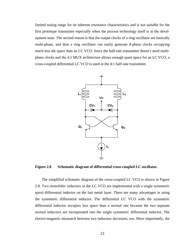
Figure 3.7 Measured VCO output waveform at (a) 11.7 GHz and (b) 18.1 GHz..... 32
Figure 3.8 Measured frequency-voltage characteristics varying the differential
control voltage with a fixed varactor control voltage. ............................. 33
Figure 3.9 Measured frequency-voltage characteristics varying the varactor control
voltage with a fixed differential control voltage...................................... 33
Figure 3.10 Measured VCO output spectrum when the VCO is tuned at 19.7 GHz. . 34
Figure 3.11 Phase noise measurement when the VCO is tuned at 16.0 GHz. ............ 35
vi

Figure 3.12 Phase noise measurement when the VCO is tuned at 20.0 GHz. ............ 35
Figure 3.13 Ring VCO Performance summary........................................................... 36
Figure 4.1 Continuous linear model of the PLL. ...................................................... 37
Figure 4.2 PFD block diagram. ................................................................................. 38
Figure 4.3 Input-output timing diagram of the PFD. ................................................ 38
Figure 4.4 Block diagram of the Master-Slave flip-flop in the PFD. ....................... 39
Figure 4.5 Schematic diagram of the resettable latch in the PFD............................. 40
Figure 4.6 Input-output characteristics of the PFD................................................... 41
Figure 4.7 Simulated input-output waveforms of PFD............................................. 41
Figure 4.8 Schematic diagram of the RC ladder LPF. .............................................. 42
Figure 4.9 Layout plot of the RC ladder LPF. .......................................................... 43
Figure 4.10 Pole-locations of the PLL model. ............................................................ 44
Figure 4.11 Bode plot of the PLL model. ................................................................... 45
Figure 4.12 Nyquist plot of the PLL model. ............................................................... 46
Figure 4.13 Step response of the continuous linear model of the PLL. ...................... 48
Figure 4.14 Step response of the schematic design of the PLL. ................................. 48
Figure 4.15 Simulated PLL locking acquisition process. ........................................... 49
Figure 4.16 PLL tracking performance simulation. .................................................... 50
Figure 4.17 Measured PLL feedback signal waveforms at (a) 350 MHz (VCO at 11.2
GHz) and (b) 630 MHz (VCO at 20.16 GHz). ........................................ 51
Figure 4.18 Measured 350-MHz PLL feedback output spectrum when VCO is locked
at 11.2 GHz.............................................................................................. 52
Figure 4.19 Measured 625-MHz PLL feedback output spectrum when VCO is locked
at 20 GHz................................................................................................. 52
Figure 4.20 PLL phase noise measurement when VCO is locked at 20 GHz. ........... 53
Figure 4.21 Phase noise comparison between the VCO and the PLL at 20 GHz. ...... 54
Figure 4.22 PLL performance summary. .................................................................... 54
Figure 5.1 Simplified block diagram of the 16:1 MUX circuit................................. 56
Figure 5.2 Output bit stream of the MUX Output D1 of the 16:4 MUX (D2, D6, D10
and D14 are the 16-bit data input from the LFSR).................................. 58
vii

Figure 5.3 Block diagram of the internal 4:1 MUX of the 16:4 MUX in SERDES III
Tx............................................................................................................. 59
Figure 5.4 Timing diagram of the internal 4:1 MUX of the 16:4 MUX in SERDES
III Tx........................................................................................................ 60
Figure 5.5 Block diagram of the internal 4:1 MUX of the 16:4 MUX in the quarter-
rate transmitter. ........................................................................................ 61
Figure 5.6 Timing diagram of the internal 4:1 MUX of the 16:4 MUX in the quarter-
rate transmitter. ........................................................................................ 62
Figure 5.7 Schematic of the MUX-Latch in the internal 4:1 MUX. ......................... 63
Figure 5.8 Simulated timing diagram of the proposed internal 4:1 MUX of the 16:4
MUX in the quarter-rate transmitter. ....................................................... 64
Figure 5.9 Simulated waveforms of the LFSR outputs and the 16:4 MUX sampled
input at 6.625 Gb/s for the final serial data bit rate of 106 Gb/s. ............ 65
Figure 5.10 Simulated waveforms of the internal 4:1 MUX of the 16:4 MUX
operating at 26.5 Gb/s for the final serial data bit rate of 106 Gb/s. ....... 66
Figure 5.11 Block diagram of the Edge-Channeling 4:1 MUX and the 8-phase
clocks…... ................................................................................................ 67
Figure 5.12 Timing diagram of the Edge-Channeling 4:1 MUX................................ 68
Figure 5.13 Schematic block diagram of the Edge-Channeling 4:1 MUX. ................ 70
Figure 5.14 Layout plot of the Edge-Channeling 4:1 MUX. ...................................... 71
Figure 5.15 Output of the Edge-Channeling 4:1 MUX contains severe switching noise
in its (a) waveform and (b) eye diagram.................................................. 72
Figure 5.16 The final output of the quarter-rate transmitter after thresholding shows
its (a) waveform and (b) eye diagram free from the switching noise
problem. ................................................................................................... 72
Figure 5.17 Schematic of the final 2:1 MUX and the cascode open-collector output
buffer for thresholding............................................................................. 73
Figure 6.1 (a) The layout plot and (b) the chip microphotograph of the 16:1 quarter-
rate transmitter. ........................................................................................ 75
Figure 6.2 Power distribution of the 16:1 quarter-rate transmitter with built-in testing
circuits...................................................................................................... 77
viii

Figure 6.3 Power distribution of the pure 16:1 quarter-rate transmitter without the
testing circuits. ......................................................................................... 77
Figure 6.4 VCO frequency tuning in the post-layout simulation of the 16:1 quarter-
rate transmitter. ........................................................................................ 78
Figure 6.5 Input-output waveforms of the 16:1 quarter-rate transmitter operating at
54 Gb/s in a parasitic post-layout simulation. ......................................... 79
Figure 6.6 54-Gb/s output eye diagrams of the 16:1 quarter-rate transmitter in a
parasitic post-layout simulation............................................................... 80
Figure 6.7 67.5-Gb/s output eye diagrams of the 16:1 quarter-rate transmitter in a
parasitic post-layout simulation............................................................... 81
Figure 6.8 On-die measurement setup with multi-contact wedge probes. ................ 82
Figure 6.9 Waveforms of VCO/16 signal when the PLL is locked (a) at 10.64 GHz
and (b) at 16 GHz. ................................................................................... 83
Figure 6.10 Eye diagrams of the LFSR output when the VCO is tuned (a) at 10.64
GHz and (b) at 16 GHz............................................................................ 83
Figure 6.11 Output eye diagrams of the 16:1 quarter-rate transmitter operating (a) at
45 Gb/s and (b) at 52 Gb/s....................................................................... 84
Figure 6.12 The layout plot of the 16:1 MUX only chip incorporating pads and power
rails. ......................................................................................................... 85
Figure 6.13 80-Gb/s eye diagram of the 16:1 MUX only chip in a parasitic post-layout
simulation with an ideal clock source...................................................... 86
Figure 7.1 Schematic diagram of a cross-coupled LC VCO..................................... 90
Figure 7.2 The small-signal model of the cross-coupled LC oscillator showing
negative input resistance.......................................................................... 91
Figure 7.3 Physical shape of a monolithic inductor. ................................................. 92
Figure 7.4 Peak Q frequency vs. inductance for various outer dimensions in the IBM
0.13-µm SiGe process.............................................................................. 93
Figure 7.5 Dependence of inductance and peak Q frequency on line width............. 95
Figure 7.6 Layout plot of the 40-GHz cross-coupled LC VCO................................ 96
ix

Figure 7.7 Comparison between a DT groundplane inductor and a M1 groundplane
inductor with the Lw of 10µm, the Ls of 5µm, and the outer dimension of
200µm...................................................................................................... 97
Figure 7.8 DT groundplane inductors and substrate contacts placements. ............... 98
Figure 7.9 Layout plot of the 40-GHz symmetric cross-coupled LC VCO. ............. 99
Figure 7.10 Single-ended excitation model of a monolithic spiral inductor............. 100
Figure 7.11 Differential excitation model of a monolithic symmetric inductor. ...... 100
Figure 7.12 Schematic diagram of the 40-GHz symmetric cross-coupled LC VCO.101
Figure 8.1 Schematic diagram of an asymmetric latch. .......................................... 104
Figure 8.2 fT characteristics vs. emitter size for high-fT NPN devices in the IBM 8HP
process (from the IBM BiCMOS 8HP Model Guide). .......................... 105
Figure 8.3 Schematic diagram of a high-speed latching operation flip-flop (HLO
F/F). ....................................................................................................... 106
Figure 8.4 Flipflop-based frequency divide-by-two circuit. ................................... 107
Figure 8.5 Frequency dividers performance comparison........................................ 108
Figure 8.6 Nonsymmetrical layout plot of an asymmetric D-latch......................... 109
Figure 8.7 Symmetrical layout plot of an asymmetric D-latch. .............................. 110
Figure 8.8 Nonsymmetrical layout plot of a HLO F/F............................................ 111
Figure 8.9 Symmetrical layout plot of a HLO F/F.................................................. 112
Figure 9.1 Simplified block diagram of the 4:1 half-rate transmitter. .................... 113
Figure 9.2 Simplified block diagram of the 2:1 five-latch MUX. .......................... 114
Figure 9.3 Simplified block diagram of the HRO-MUX. ....................................... 115
Figure 9.4 Timing diagram of the HRO-MUX. ...................................................... 115
Figure 9.5 Schematic diagram of the HRO-MUX. ................................................. 116
Figure 9.6 Layout plot of the HRO-MUX. ............................................................. 117
Figure 9.7 Schematic diagram of the tree architecture 4:1 MUX. .......................... 118
Figure 9.8 Layout plot of the tree architecture 4:1 MUX. ...................................... 118
Figure 9.9 Simulated waveforms of the tree architecture 4:1 MUX operating at 100-
Gb/s........................................................................................................ 119
Figure 9.10 Simulated eye diagram of the tree architecture 4:1 MUX operating at 100-
Gb/s........................................................................................................ 120
x

Figure 9.11 Simplified block diagram of Galois 27-1 LFSR. ................................... 121
Figure 9.12 Simplified block diagram of the 27-1 LFSR with a 4-bit output. .......... 122
Figure 9.13 The layout plot of the 27-1 LFSR with 4-bit output............................... 123
Figure 9.14 Block diagram of the Johnson ring counter for a simple BER test. ...... 124
Figure 9.15 The output data pattern of the Johnson ring counter. ............................ 124
Figure 9.16 The layout plot of the Johnson ring counter for simple BER test. ........ 125
Figure 9.17 Schematic diagram of the doubly-terminated output amplifier. ............ 126
Figure 10.1 (a) The layout plot and (b) the chip microphotograph of the 4:1 half-rate
transmitter with the PLL and the LC VCO............................................ 128
Figure 10.2 (a) The layout plot and (b) the chip microphotograph of the 4:1 half-rate
transmitter with the ring counter and the external clock input pad. ...... 129
Figure 10.3 Power distribution in the 4:1 half-rate transmitter with the built-in testing
circuits.................................................................................................... 130
Figure 10.4 Power distribution of the pure 4:1 half-rate transmitter without the testing
circuits.................................................................................................... 130
Figure 10.5 Eye diagrams of the 4:1 half-rate transmitter driven by an external clock
at various frequencies in post-layout simulations.................................. 132
Figure 10.6 81-Gb/s eye diagrams of the 4:1 half-rate transmitter with the built-in LC
VCO in a post-layout simulation. .......................................................... 133
Figure 10.7 80-Gb/s half-eye diagram of the 4:1 half-rate transmitter with the Johnson
ring counter input pattern in a post-layout simulation........................... 133
Figure 10.8 Cable attenuation. .................................................................................. 134
Figure 10.9 50-GHz probe circuit model. ................................................................. 135
Figure 10.10 Probe AC frequency response. .............................................................. 136
Figure 10.11 80-Gb/s eye diagram with a 8 inches cable. .......................................... 136
Figure 10.12 80-Gb/s eye diagram with a 12 inches cable. ........................................ 137
Figure 10.13 80-Gb/s eye diagram with a 20 inches cable. ........................................ 137
Figure 10.14 80-Gb/s eye diagram with a 30 inches cable. ........................................ 137
Figure 10.15 60-Gb/s eye diagram with 12 inches cable. ........................................... 138
Figure 10.16 70-Gb/s eye diagram with 12 inches cable. ........................................... 138
Figure 10.17 85-Gb/s eye diagram with 12 inches cable. ........................................... 138
xi

Figure 10.18 Eye opening summary according to cable lengths and data rates. ........ 139
Figure 10.19 Comparison of the data sequences in the simulation and the
measurement... ....................................................................................... 140
Figure 10.20 40-Gb/s waveform of the 4:1 half-rate transmitter. ............................... 141
Figure 10.21 50-Gb/s waveform of the 4:1 half-rate transmitter. ............................... 141
Figure 10.22 60-Gb/s waveform of the 4:1 half-rate transmitter. ............................... 142
Figure 10.23 66-Gb/s waveform of the 4:1 half-rate transmitter. ............................... 142
Figure 10.24 Measured RMS jitter of 831-fs on the 4:1 half-rate transmitter operating
at 60-Gb/s............................................................................................... 143
Figure 11.1 A comparison of measured key performance parameters...................... 146
Figure 11.2 Comparison of power distributions between a pure 4:1 quarter-rate
transmitter and a pure 4:1 half-rate transmitter. .................................... 147
Figure 11.3 Comparison with the state of the art designs. ........................................ 148
xii

ABSTRACT
High-speed serial communication technology is in great demand to keep pace with the
explosive increase of the data rate in digital data communication. The goal of this work
is to design a leading edge high-speed serial data transmission circuitry utilizing a 0.13-
µm SiGe BiCMOS technology. Two different clocking approaches are made to investi-
gate possibilities. A 52-Gb/s 16:1 quarter-rate transmitter and a 66-Gb/s 4:1 half-rate
transmitter are designed, fabricated, tested, and then compared. Both the transmitters
achieve higher data rates than the state of the art with less power consumption.
The 16:1 quarter-rate transmitter consists of a 16:1 multiplexer (MUX), a voltage-
controlled ring oscillator, a phase-locked loop (PLL), a pseudo-random data generator,
and an output amplifier. The voltage-controlled ring oscillator shows a wide tuning
range from 12 to 23 GHz with hybrid control schemes and a low phase noise of –104.8
dBc/Hz at 1 MHz offset. The VCO phase noise is stabilized as –124.6 dBc/Hz at 1 MHz
offset by a third-order PLL. A continuous model of the third-order PLL is developed and
used to optimize loop filter parameters and to estimate the PLL performance in a simula-
tion. The 16:1 MUX features quarter-rate clock multiplexing with the multi-phase output
VCO. In the design of a 16:4 MUX, total transition delay is reduced with fewer transis-
tors used. Edge-Channeling 4:1 multiplexer is used to alleviate a duty cycle problem.
The 4:1 half-rate transmitter consists of a 4:1 MUX, an LC VCO, a PLL, and a
built-in testing circuit. A 40-GHz cross-coupled LC VCO is designed with a single
symmetric high-Q inductor. A novel high-speed F/F, HLO F/F, is designed and com-
pared with conventional designs. A symmetric high-speed 4:1 MUX is designed with
newly proposed 2:1 high-speed retiming MUXs (HRO-MUXs). The HRO-MUX
achieves bandwidth improvement due to high-speed data retiming. The 4:1 half-rate
transmitter shows an output data rate of 66 Gb/s with a data duty cycle of 53% due to the
HRO-MUXs. A simple bit-error rate (BER) testing is performed with a built-in ring-
counter. Power consumption of the 4:1 half-rate transmitter even with a built-in testing
data generator is no more than 1.57 W, which is less than that of state of the art.
xiii

Part I. INTRODUCTION
1

1. Introduction
1.1 Introduction to SERDES
For a long time, parallel communication or parallel bus has been mainly used in com-
puter systems because serial communication has been considered to be slower than
parallel communication. Serial communication has been used only in some applications
with a long-distance connection to save costs for wires. The representative application is
the telephone network and the computer network. However, as the IC speed increases
and the bus bandwidth rapidly grows, the parallel communication reaches its limits.
During the past decade, serial communication has evolved quickly and its use becomes
widespread. At the present time, serial communication has higher bandwidth and costs
much less than a standard parallel communication, and thus most high-speed interfaces
have switched to serial communications. Therefore, serial communication has come to
dominate all around from some centimeter applications to some thousand kilometer
applications.
In telecommunication network, the increasing demand for higher digital data trans-
mission has been expediting the development of a high-speed serial communication
[1][2]. The increasing data bit width such as 32 or 64 bits in computer systems has also
necessitated the development of the high-speed serial communication. Above all, the
widespread nature of the Internet made an explosive increase in demand for the high-
speed serial communication. An optical serial communication transmits and receives
point-to-point non-return-to-zero (NRZ) data through hundreds of kilometers over fiber
for long-haul transport of synchronous optical network (SONET) [1].
In short-haul applications like a computer system bus or a hard-disk interface, a par-
allel bus has been used for a long time. However, as a transmission bandwidth grows
rapidly, timing becomes the fundamental reason to prevent the speedup of a parallel bus.
In a parallel communication, all the parallel data should be arrived almost at the same
time to synchronize with a bus clock [3]. However, each bit channel tends to delay by
each different amount of skew that is caused by line or load impedance. As the fre-
2

quency of a transmitted signal increases, the skew becomes more critical with the growth
of parasitic impedances. Figure 1.1 shows the skew in a parallel bus.
Figure 1.1 Skew across a high-speed parallel bus limits the bandwidth of the bus.
In Figure 1.1, because of a skew in the Bit 2 channel, the setup-hold time should be
adjusted, and it narrows a timing window when a clock edge can occur. Consequently,
the skew limits the parallel bus speed. A serial bus structure can solve this critical skew
problem because a serial bus is self-clocking, and there is no skew between data and
clock; precisely a clock signal is not transmitted. The other advantage of a serial bus is
the reduced number of IC pins. Although a serial bus structure could demand more
complex circuitries than a parallel bus structure, transistors are cheap and pins are
expensive in modern IC chips [3].
For the reasons mentioned above, serial communications are dominant in modern
high-speed interfaces. As a processor speed broke through GHz barrier in computer
systems, computer systems became one of the highest-speed application areas. In
computer systems, most interfaces become serial. For example, old parallel PCI periph-
3

eral bus is superseded by new serial PCI-Express peripheral bus. Old parallel ATA
(PATA) bus for a hard-disk interface is being replaced by new serial ATA (SATA) bus.
Figure 1.2 Typical block diagram of a serial data communication system.
A general serial data communication system consists of a serializer, a linkage me-
dium, and a deserializer. Figure 1.2 shows a typical block diagram of a serial data
communication system. A serializer is also called a transmitter (Tx), and a deserializer is
called a receiver (Rx). A serializer/deserializer is simply called SERDES.
A transmitter receives parallel input data from a sender. A sender can be a backbone
router, a computer, a CPU, an I/O chip, or something else according to each application.
The multi-channel parallel input data are multiplexed by the transmitter and become a
high-speed serial data stream. For example, if a sender transmits 2-Gb/s 16-bit inputs
through a 16:1 transmitter, the serial data stream from the transmitter will have 32-Gb/s
data rate. The task of parallel-to-serial conversion is performed by a multiplexer (MUX)
in the transmitter. The MUX should be synchronized with a system clock generated by a
clock multiplication unit (CMU) that incorporates a VCO, a PLL and a clockpath.
A deserializer receives a serial data stream and converts the serial data to the origi-
nal parallel data using an incorporated demultiplexer (DMUX). A clock for the
demultiplexer should be synchronized with the system clock in the transmitter to recover
the correct data sequence, but any additional clocking information is generally not
transmitted from the transmitter. Consequently, the receiver should recover from the
4

incoming data signals an internal clock of which frequency is matched with that in the
transmitter. The overall recovery operation is called “clock and data recovery” (CDR).
A serial data stream is generally a non-return-to-zero (NRZ) digital to increase the
data rate of a serial communication. If a transmitted data stream has too long runs of one
or zero pattern, clock recovery becomes very difficult to achieve for the increase in
intersymbol interference (ISI). In order to prevent such a problem, transmitted data are
generally encoded to be “dc-balanced” having equal numbers of one or zero pattern. A
typical encoding method is 8B/10B coding mapping an 8-bit word to a 10-bit word.
Most modern high-speed serial communications use this coding.
1.2 Applications
As mentioned, a serial communication comes to dominate in most high-speed applica-
tions. The physical length of the communication linkage medium usually classifies serial
communications. For example, the linkage medium could be a few tens of centimeters
for chip-to-chip data transmission on a printed circuit board (PCB) or hundreds of
kilometers over fiber for long-haul transport in the synchronous optical network
(SONET) frames [1].
The representative examples of long-haul serial communications are SONET and
Gigabit Ethernet. The SONET is a standard for optical telecommunications formulated
by the Exchange Carriers Standards Association (ECSA) for the American National
Standards Institute (ANSI). The SONET defines the standard for communicating digital
information optically using lasers or light emitting diodes (LEDs) over optical fiber. The
SONET was developed to replace the Plesiochronous Digital Hierarchy (PDH) system
for transporting large amounts of telephone and data traffic. The SONET differs from
the previous PDH in that the exact data rates are tightly synchronized by atomic clocks
across the entire network [4] while the SONET is self-clocking utilizing a clock and data
recovery (CDR). As shown in its name, the SONET is point-to-point synchronous
network, greatly reducing the amount of buffering that is required between each element
in the network.
5

Figure 1.3 Synchronous optical network (SONET) ring architecture based on a high-speed optical serial communication.
Figure 1.3 shows a common ring architecture of the SONET. The SONET is basi-
cally a point-to-point serial communication. The SONET add/drop multiplexer (ADM) is
a unique element designed to enable point-to-multipoint networking in the SONET.
Among the SONET standards, 10-Gb/s OC-192 and 40-Gb/s OC-768 are recently more
of interest for high demand [5]. The commercial state of the art for the SONET is the
OC-192 for 10-Gb/s serial links.
The Gigabit Ethernet is another example of the high-speed long-haul serial commu-
nication, and it is designed for the broadband local area networks (LAN). The Gigabit
Ethernet defines the standard of various technologies for transmitting Ethernet packets at
a rate of 1 Gb/s. “10 gigabit Ethernet” or “10GbE” is the most recent and fastest of the
Ethernet standards until 2006. The 10GbE defines a version of Ethernet with a nominal
data rate of 10 Gb/s. The 10GbE can transmit 10-Gb/s data through fibre or even through
copper.
6
Examples of the short-haul serial communications are numerous. A parallel
supercomputer uses a high-speed serial communication to link hundred of parallel
processors and thousand of I/Os. One of the most widely used standards is InfiniBand

and thousand of I/Os. One of the most widely used standards is InfiniBand that has high
bandwidth of 2.5 Gb/s. The InfiniBand is primarily used in a computer cluster. A com-
puter cluster is a modern parallel supercomputer structure grouping loosely coupled
computers as shown in Figure 1.4. A computer cluster becomes dominant for its higher
speed, better reliability, and most importantly lower cost. The InfiniBand standard
defines connections between processor nodes and I/O nodes such as storage devices in a
computer cluster.
Figure 1.4 A parallel supercomputer grouping many computers linked by high-speed serial interconnections.
Flat panel display (FPD) interface is also a good example of the short-haul serial
communication. A FPD interface connects a digital display panel with a computer, a set-
top box or any digital image source. The most dominant standard is DVI and its succes-
sor HDMI. As the resolution of a FPD increases, the demanded bandwidth grows rapidly.
For example, in NEC Co., Japan, an ultra-high-resolution (3200 × 2400 pixels) FPD
needed to have an interface link with a bandwidth of 16 Gb/s [6]. So, they designed 20-
Gb/s multichannel transmitter and receiver chipset for the ultra-high-resolution digital
display. On the other hand, as the resolution of digital image sources increases, the
bandwidth of a FPD interface grows. High-definition videos on Blu-ray or HD DVD
format demand the very high bandwidth of serial communication.
7

Figure 1.5 Various applications of the short-haul serial communication.
The most popular application area of the short-haul serial communication is the
computer. In a computer, there is a general trend from a parallel communication to a
serial communication, for example, PCI Express, Serial ATA, HyperTransport, USB, or
IEEE 1394. PCI Express supersedes the old PCI standard as the peripheral bus in a
computer. The old PCI has a parallel bus with the maximum data rate of 133 MB/s. The
new PCI Express has multi-channel serial links with maximum combined data rate of 4
GB/s. Serial ATA is a new storage interface standard to supersede the old parallel ATA.
Serial ATA provides a high-speed serial communication link between a computer system
board and a hard-disk drive or an optical drive.
As mentioned before, the linkage medium of a high-speed serial communication
could be a few tens of centimeters for chip-to-chip data transmission on a printed circuit
board (PCB). HyperTransport or RapidIO technology provides a point-to-point high-
speed serial communication link between ICs on a PCB. Both of them are packet-based
serial links, and thus they are very scalable and flexible. Packets are routed by a crossbar
switches, and a high-speed crossbar switch design is highly demanded, too.
8

1.3 State of the Art
In order to assemble a high-speed serial transmitter, three basic components should be
designed. They are a multiplexer (MUX), a voltage-controlled oscillator (VCO), and a
phase-locked loop (PLL). Most recent research is focused on optical serial communica-
tion, the SONET, since it is most challenging and demands the highest data rate. To the
best of our knowledge, until recently, the highest data rate of a serial IC transmitter is 43
Gb/s [7][8][9][11], and naturally higher data rate has been reported in each independent
component design. Unless restricted to a fully IC transmitter, 107-Gb/s NRZ signal
transmission is demonstrated over 400 km with various high-speed digital module
packages [17]. Those high-speed digital modules are designed in SiGe or III-V com-
pounds technology such as GaAs, InP and InGaAs. However, a fully combined IC
transmitter is highly demanded for smaller dimensions, less power consumption, and
most importantly less cost.
A fully integrated 43-Gb/s 16:1 transmitter is designed in 0.18-µm SiGe BiCMOS
technology [7] at Hitachi Ltd., Japan. The Hitachi transmitter uses full-rate clocking with
integrated 43-GHz VCO. Full-rate, half-rate, or quarter-rate clocking concepts are
described in Chapter 2.1. The Hitachi transmitter has an advanced PLL design with dual
loops to lower MUX output jitter to 630 fs rms. Another feature of the Hitachi transmit-
ter is that the 43-GHz clock is generated by a frequency doubler with a 21.50-GHz LC
oscillator. A half-rate clocking 43-Gb/s OC-768 16:1 transmitter is designed in 0.18-µm
SiGe BiCMOS technology at Big Bear Networks, CA [9]. The Big Bear Networks
transmitter has two copackaged ICs, 16:4 MUX and 4:1 MUX/CMU [8]. The transmitter
has 20-GHz quadrature-coupled LC-type VCO for an advanced quadrature clocking
final MUX circuitry. A full-rate and half-rate clocking 4:1 transmitter is designed in
0.18-µm SiGe BiCMOS technology at IBM, NY [10][11]. The IBM half-rate transmitter
shows a low data jitter of 540 fs rms while the IBM full-rate transmitter shows a data
jitter of 600 fs rms. The IBM half-rate transmitter consumes less power by 30% than the
IBM full-rate transmitter. They show that a carefully designed half-rate transmitter can
achieve better performance even at lower power consumption than an equal-speed full-
rate transmitter. All of the above latest transmitters are designed in 0.18-µm SiGe
9

BiCMOS technology. Although not a single lane, a 20-lane 62.5-Gb/s SERDES with a
single lane data rate of 3.125 Gb/s is designed in 0.13-µm CMOS technology [12]. The
CMOS SERDES incorporates a 4:1 MUX and a 1:4 DEMUX. Even though CMOS
technology has been improved quickly, still all the very high-speed circuits are imple-
mented in a SiGe BiCMOS technology for the much higher fT and fmax.
A VCO is a critical component in order to realize a fully integrated transmitter.
VCOs themselves have achieved very high oscillation frequency such as 122 GHz [13].
However, their performances degenerate greatly when connected with practical loads
due to back-propagated impedance loads. A ring oscillator VCO design is very attractive
due to wide tuning range and small on-chip size. Since a ring oscillator passes through
multiple buffer stages, the maximum oscillation frequency of a ring oscillator is gener-
ally limited to approximately fmax/10 of the device [21]. Although of the limited
oscillation frequency, a ring oscillator has a unique intrinsic advantage of precise multi-
phase clocking generation. Multi-phase clocking enables to design a quarter-rate clock-
ing transmitter with low frequency clocks. An 8-phase 2.5-GHz VCO is used to
sequentially latch incoming data bits in a receiver chip for 10-Gb/s serial data transmis-
sion [23]. An 8-phase 5-GHz feedforward interpolated VCO is used to transmit data in
excess of 20-Gb/s in a serial transmitter [24].
An LC VCO is fundamentally based on passive resonant circuits, and thus an LC
VCO does not achieve a wide tuning range when compared with a ring oscillator.
However, an LC VCO has been more frequently used to design a high-speed serial
transmitter with fixed transmission data rate due to its significantly low phase noise.
Separated LC VCOs with little driving loads show outstanding performances of high
oscillation frequency and low phase noise. A 120-GHz push-push LC-Varactor VCO
with the tuning range of 8.5% is designed in a SiGe BiCMOS technology with 155-GHz
fT [13]. A 21.5/43-GHz dual frequency LC VCO is designed in a 0.25-µm SiGe tech-
nology [15]. The dual frequency LC VCO has the peculiar characteristics of a push-push
VCO such that the differential output has 21.5-GHz frequency while the single-ended
output has 43-GHz frequency at the same time. Even in a 0.25-µm CMOS technology, a
63-GHz LC VCO is reported [14]. However, the CMOS LC VCO shows a high phase
noise of –85 dBc/Hz at 1 MHz offset even without an output amplifier load. A lower
10

phase noise 44-GHz CMOS LC VCO is designed in a 0.12-µm SOI CMOS [16]. The
44-GHz VCO achieves wider tuning range of 9.8% with a differential tuning method and
low phase noise of –101.8 dBc/Hz at 1 MHz.
We next survey practical usages of LC VCOs with a PLL and driving loads. A 12.5-
GHz differential LC VCO with cross-coupled topology is used with a PLL to provide a
full-rate system clock with 0.4ps rms jitter for a 12.5-Gb/s serial transmitter [2]. A 20-
GHz CMOS LC VCO with quadrature phase outputs is used with a PLL to provide a
half-rate system clock for a 40-Gb/s CMU operation [5]. A quadrature-coupled 20-GHz
LC VCO with a PLL provides quadrature clocks to a 40-Gb/s multiplexer in a 16:1
transmitter [9]. As pointed out earlier, performance of a VCO and a PLL degenerates
significantly in a practical application for large load impedance. Therefore, the driving
capability is a practically important measure to estimate the performance of a VCO and a
PLL.
There are many high-speed multiplexers reported. A 54-Gb/s 4:1 MUX is designed
in a 0.2-µm SiGe technology [40]. The 54-Gb/s MUX is driven by an external full-rate
clock from a signal generator, and thus the MUX can perform output data retiming to
reduce output jitter. An 80-Gb/s 4:1 MUX is designed in a 0.13-µm SiGe BiCMOS
technology [39]. The 80-Gb/s MUX uses many inductively peaked latches and selectors,
which requires a big chip size of 3.5 mm by 3.5 mm and a large power consumption of
9.8 W. Notably, adjustable delay cells are inserted into clock paths to match timing and
those cells are manually tuned when tested. The reported highest data rate of a MUX is
132-Gb/s from a half-rate clocking 4:1 MUX in a 0.13-µm SiGe Technology [43].
Inductive peaking is used in the clockpath. The input data and the system clock are
provided by an external PRBS generator and an external signal generator. Most high
performances are demonstrated only with a 4:1 MUX. A conventional architecture of
high-speed 4:1 MUX is a tree architecture consists of three 2:1 MUX. A five-latch MUX
is one of the most widely used 2:1 MUX design [39][40][43]. In order to save power or
space, the number of latches can be reduced to three from five[41]. All the above MUXs
are operating at very high data rate, but their great performances are achieved with
strong and clean external clock signals besides external input data. When combined with
11

an on-chip CMU, their practical performances degenerate severely as VCOs degenerate
in practical usages.
1.4 Goals and Design History
The goal of this research is to design a leading edge high-speed serial data transmission
circuitry utilizing the latest SiGe BiCMOS technology, IBM 0.13-µm SiGe process. In
order to overcome many challenging problems occurred in two-digit number GHz world,
all the integrated circuits should be designed to operate at the edge of the limit. In this
research, all the ICs are designed, developed, and tested only by the author. For the
shortage of manpower, the research is focused on the design of a transmitter system.
Two approaches are made to design transmitters with two clocking schemes, a quarter-
rate clocking scheme and a half-rate clocking scheme.
Although the two proposed SiGe high-speed transmitters target a short-haul distance
application such as a serial communication link in a parallel supercomputer system, the
proposed circuits could be adapted to a long-haul distance application such as optical
communication. Since this research is dedicated to exploration of a possible highest data
rate transmitter rather than to commercialization of the technology, the design does not
consider much about power consumption, which is one of the most critical considera-
tions in commercial integrated circuits. However, the designed transmitters achieve less
power consumption than that of the state of the art.
Three major IC fabrications have been done in the MOSIS service for the research.
The first IC chip, a wide tuning range VCO was submitted in September 2004, and
returned in January 2005. The VCO chip has been tested and analyzed providing much
insight into the possibility of the process technology for the next advanced designs. The
measurement results were published in IEEE Annual Symposium on VLSI in May 2005
[20]. The second fabrication was made in January 2005. The second IC chip, a quarter-
rate clocking 16:1 transmitter, is an all-in-one transmitter including a PRBS data genera-
tor, that is, a 231-1 16-bit LFSR. The quarter-rate clocking transmitter incorporates a ring
oscillator, a PLL, and a 16:1 MUX, too. The fabricated quarter-rate clocking transmitter
12

chip was tested in June 2005. After the second IC submission, a new architecture trans-
mitter design was started based on half-rate clocking scheme. The third IC chip, a half-
rate clocking 4:1 transmitter, was fabricated in December 2005. The half-rate clocking
transmitter incorporates a differential LC VCO, a PLL, a high-speed 4:1 MUX, and two
built-in testing circuits of a 27-1 4-bit LFSR and a Johnson ring counter. The fabricated
half-rate clocking transmitter was tested in May 2006. Some minor IC fabrications are
done between each major fabrication to patch and complete the designs.
13
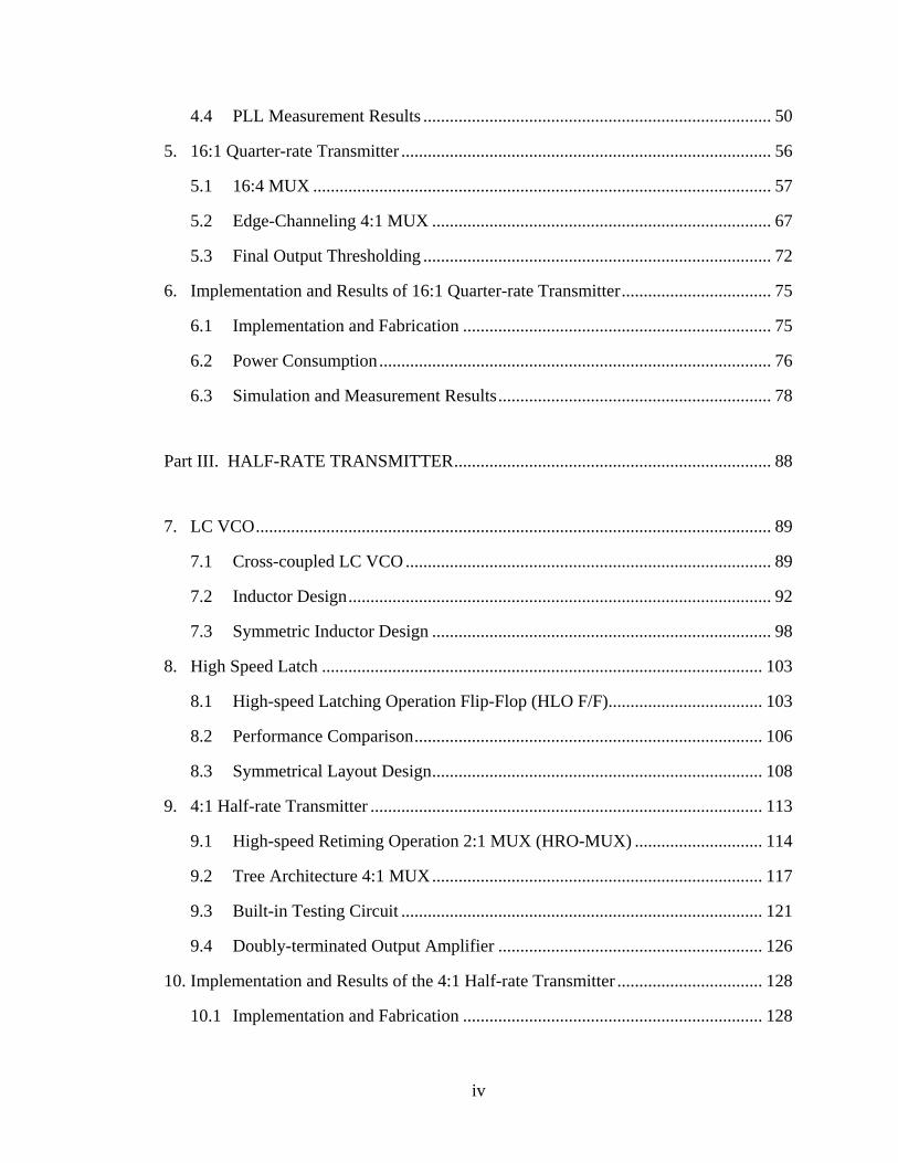
2. Architecture Overview
2.1 Clocking Schemes
Architecture of transmitters can be classified in various ways according to multiplexing
method, clocking scheme, and etc. If transmitters are classified by their clocking
schemes, there are commonly full-rate, half-rate, or quarter-rate clocking transmitters. If
a transmitter can serialize parallel data channels into N b/s serial output stream with N
Hz clock, it is a full-rate clocking transmitter. The other clocking schemes are defined in
the same way. For example, the 80-Gb/s half-rate transmitter uses 40-GHz clock. In this
work, a 66-Gb/s half-rate clocking transmitter and a 52-Gb/s quarter-rate transmitter are
designed in a 0.13-µm SiGe process. From Figure 2.1 to Figure 2.3, three architectures
of 80-Gb/s transmitters are shown in order to compare each clocking schemes.
Figure 2.1 Block diagram of the 4:1 full-rate clocking transmitter.
14

Figure 2.2 Block diagram of the 4:1 half-rate clocking transmitter
Figure 2.3 Block diagram of the 16:1 quarter-rate clocking transmitter.
Figure 2.1 shows a common architecture of a 4:1 full-rate clocking transmitter. The
80-Gb/s full-rate transmitter is driven by a 80-GHz clock from a clock multiplier unit
(CMU). A CMU conventionally incorporates a phase-locked loop, a VCO, and a clock-
path. The greatest advantage of the full-rate clocking architecture is that a retimer is
available after the last MUX. A conventional retiming circuit is flip-flop shown in
Figure 2.1. The retimer can compensate for jitter noise produced by latches, multiplexers,
and the CMU. However, the full-rate clocking scheme suffers from the necessity of
15

high-speed design components such as a full-rate 80-Gb/s flip-flop and a full-rate 80-
GHz frequency divider for 80-Gb/s transmission. In fact, the 80-GHz CMU itself is very
difficult to design. Additionally, the full-rate clocking transmitter is more power hungry
than the other clocking transmitters.
Figure 2.2 shows a common architecture of a 4:1 half-rate clocking transmitter. An
80-Gb/s half-rate transmitter is driven by a 40-GHz clock, and thus a CMU doesn’t need
to operate at very high frequency. Also, the amount of load seen by the CMU is reduced,
and the CMU can operate with less distortion. However, because a half-rate clocking
transmitter cannot use a final retimer, it is unavoidable that duty cycle distortion of the
half-rate clock is directly transferred to the final serial output of the transmitter. There-
fore, the final output jitter noise of the half-rate scheme could be higher than that of the
full-rate scheme.
Figure 2.3 shows the architecture of a 16:1 quarter-rate clocking transmitter. Be-
cause a clock has the quarter frequency of the full-rate data rate, the quarter-rate
clocking scheme needs multi-phase clocks, namely quadrature clocks. In the quarter-rate
transmitter designed in this work, a CMU is designed with current mode logic (CML),
and thus the CMU supplies differential quadrature clocks that are 8-phase. With the
increased number of clock phases, it becomes easy to expand the transmitter as a 16:1
MUX architecture. The advantage of a quarter-rate clocking scheme is the much lower
frequency of the clocks. A ring oscillator is chosen as a VCO to generate such slow
multi-phase clocks.
Half-rate clocking transmitter and quarter-rate clocking transmitter are abbreviated
as half-rate transmitter and quarter-rate transmitter in the following chapters.
2.2 16:1 Quarter-rate Transmitter Architecture
A 16:1 quarter-rate transmitter utilizing a multi-phase clocking scheme is designed in the
IBM 8HP 0.13-µm SiGe-bipolar process with 210-GHz fT.
16

Figure 2.4 Block diagram of the 16:1 quarter-rate transmitter.
Figure 2.4 shows the system block diagram of the quarter-rate transmitter. The quar-
ter-rate transmitter is an all-in-one chip including a built-in testing circuit (linear
feedback shift register) and a clocking circuitry (phase-locked loop).
The linear feedback shift register (LFSR) generates 16-bit input data for testing. The
LFSR parallel data are converted to a serial bit-stream by a 16:4 multiplexer (MUX) and
a 4:1 multiplexer. An output amplifier amplifies the final serial bit-stream enough to
drive an external 50-Ω impedance load. Global clocks are generated from a VCO
combined with a phase-locked loop (PLL). The PLL locks the VCO to be more stable
and have less jitter noise. The transmitter is basically a 16:1 multiplexer, and the data bit
rate increases gradually from the input stage to the output stage. The output bit rate of
the LFSR is N/16 Gb/s at the beginning stage. The next output bit rate of the 16:4 MUX
is N/4 Gb/s, and the final output bit rate of the 4:1 MUX is N Gb/s. The transmitter has a
quarter-rate clocking scheme. One of the advantages of the multi-phase clocking scheme
is that the global clock rate doesn’t need to be as fast as the final output bit rate. In
Figure 2.4, while the final output bit rate is N Gb/s, the VCO frequency is as slow as N/4
GHz.
Rensselaer Polytechnic Institute is not equipped with a necessary high-speed paral-
lel data generator for testing, and the transmitter must have a built-in testing data
generator on the IC chip itself. A linear feedback shift register (LFSR) can generate
17

pseudorandom bit stream (PRBS) data. The PRBS data are 16 bits wide. The LFSR is
synchronized with a 16:4 multiplexer (MUX) as shown in Figure 2.4, so that the 16:4
MUX can sample the PRBS input data with the right timing. The LFSR has 31 registers
to generate a 231-1 PRBS pattern. Such a long PRBS test sequence is required to get a
fully tested eye diagram of the transmitter output. 231-1 or 215-1 PRBS test pattern is
usually used to get an eye diagram of a digital signal. In most practical applications of
SERDES, transmitted data are encoded in a special way to be dc-balanced since a long
run of ‘1’ or ‘0’ could block clock recovery in a CDR or increase jitter noise. The most
widely used encoding scheme is 8B/10B coding that converts a 8-bit word to a 10-bit
word while guaranteeing a maximum run length of 5 bits. This encoding scheme keeps
dc-balancing with 25% overhead. The 231-1 PRBS pattern from the LFSR is dc-balanced
with a much longer maximum run length than that of 8B/10B encoding, which means the
LFSR output pattern is not so well dc-balanced as 8B/10B coding. Therefore, if the
transmitter operates correctly with the LFSR output pattern, the transmitter is going to
show better performance in practical applications.
Figure 2.5 Block diagram of the PLL.
All the global clocks are generated by the phase-locked loop (PLL). The PLL is
used in the transmitter to reduce jitter noise in the clocks. The PLL incorporates a 3-state
phase-frequency detector (PFD), an RC ladder low-pass filter (LPF), a voltage controlled
oscillator (VCO), and a feedback frequency divider. The PLL has conventional feedback
control architecture as shown in Figure 2.5. The PFD detects phase or frequency differ-
ence between a reference clock signal and a feedback clock signal. This difference is
18

equivalent to “error” in feedback control. The error signal is applied back into a VCO to
adjust the oscillation frequency, but the error signal contains an undesirable high-
frequency component that makes the VCO oscillation deviate rapidly from the reference.
In order to control the VCO oscillation, we need a LPF between the PFD and the VCO
that filters out the high-frequency component.
A reference clock from an external oscillator is usually much slower than the VCO
clock. If we can apply such a fast and stable reference clock as the VCO clock, we don’t
need to use a PLL in the transmitter. That means a frequency divider should be added in
the feedback path to convert the VCO clock signal into a correct feedback signal. The
frequency divider is a ÷32 divider. If we need a 20 GHz VCO clock, we must apply an
external 625 MHz reference clock.
The PLL incorporates a feedforward interpolated VCO with a varactor diode capaci-
tance load. The basic schematic design is based on the feedforward interpolated VCO
designed by Thomas W. Krawczyk [24]. The proposed VCO design in this work uses a
varactor diode as a capacitance load to finely tune the oscillation frequency. The VCO
has two control inputs for the hybrid control scheme. The VCO uses feedforward
interpolation topology for coarse frequency tuning, and a varactor diode load capaci-
tance variation for fine frequency tuning. A delay buffer in the four-stage ring oscillator
is designed with differential CML and has differential-pair output. The VCO, therefore,
has quadrature differential-pair (8-phase) outputs. The 8-phase outputs from the 20-GHz
VCO can be used in a novel serial transmitter design to transmit data in 80-Gb/s data
rate.
The 16:4 multiplexer consists of four internal 4:1 multiplexers as shown in Figure
2.6. The 16:4 multiplexer is driven by the quadrature clocks from the PLL. Each clock
phase is supplied to each internal 4:1 multiplexer. Each internal 4:1 multiplexer itself
generates the half-frequency clock and the quarter-frequency clock from each full-
frequency clock. For example, if the VCO generated a 20-GHz clock, the half-frequency
clock is 10 GHz, and the quarter-frequency clock is 5 GHz. The 231-1 LFSR is synchro-
nized with the 5-GHz quarter-frequency clock of the first internal 4:1 multiplexer to
generate the 16-bit PRBS input data with the right timing. Each internal 4:1 multiplexer
processes 4 bits out of the 16 bits from the LFSR. Each sequential output of the 16:4
19

multiplexer is phase-shifted by 90 degrees, so that they can be combined into a serial
data stream later in the final 4:1 multiplexer as shown in Figure 2.4. Therefore, if the
PLL generates 20-GHz clock, the output data rate of the final 4:1 multiplexer is 80 Gb/s.
The 16:4 multiplexer design in the 16:1 quarter-rate transmitter is based on the SERDES
III Tx design [19], but many new improvements are made. In the newly proposed design
of the internal 4:1 MUX, most data are sampled at the center of the valid data timing,
and the total transition delay of the multiplexer is reduced. Additionally the total number
of transistors used in the multiplexer is reduced.
Figure 2.6 Block diagram of the 16:4 multiplexer.
The final 4:1 multiplexer design in the 16:1 quarter-rate transmitter is based on the
Edge-Channeling MUX [19]. The greatest advantage of the Edge-Channeling MUX is
that only the first-tier multiplexers generate all the critical edges, and the rest of the
multiplexers are used to “channel” these edges to the output. Although the architecture
of the Edge-Channeling 4:1 multiplexer requires more 2:1 multiplexers than a general
4:1 multiplexer, it can alleviate a duty cycle problem and a jitter problem to the greatest
extent possible [19]. But, when the Edge-Channeling Multiplexer is used at very high
clock rate, it causes a critical problem of “undesirable switching noise channeling”. In
20

the newly proposed final 4:1 multiplexer, a cascode amplifier is added after the final 2:1
multiplexer to perform thresholding and remove the undesirable switching noise. A
current mirror as a constant current source for the cascode amplifier is isolated from all
the other circuits to prevent the switching noises from being transferred through the
voltage reference line. Also, constant current sources for internal 2:1 multiplexers are
separated from each other to alleviate the switching noise problem.
Details of each design block are described in each corresponding chapter. The de-
sign and the measurement results of the hybrid control VCO are described in Chapter 3.
The design and the measurement results of the PLL are described in Chapter 4. The
overall design of the quarter-rate transmitter is described in Chapter 5. Finally, the
simulation and measurement results of the quarter-rate transmitter are described in
Chapter 6.
2.3 4:1 Half-rate Transmitter Architecture
Figure 2.7 Block diagram of the 4:1 half-rate transmitter.
21

A 4:1 half-rate clocking transmitter is designed utilizing the IBM 8HP 0.13-µm SiGe-
bipolar process like the 16:1 quarter-rate clocking transmitter. The 4:1 half-rate transmit-
ter has the half-rate clocking scheme shown in Figure 2.2. In the half-rate clocking
scheme, a PLL is supposed to provide a 40-GHz clock to a 4:1 MUX if the final output
data rate of the 4:1 MUX is 80-Gb/s. The half-rate clocking scheme doesn’t require
multi-phase clocks, and thus a single-phase differential LC VCO can be used in the half-
rate transmitter. Figure 2.7 shows the simplified block diagram of the 4:1 half-rate
transmitter. The 4:1 half-rate transmitter consists of a built-in testing circuit, three 2:1
multiplexers, an output amplifier, and a clockpath. A clockpath incorporates an LC VCO,
a PLL, a frequency divider, and clocking buffers.
For the lack of a high-speed multi-channel signal generator, a testing data generator
is built on the IC chip providing 4 bits of parallel input data to the 4:1 half-rate transmit-
ter. The testing data generator is a LFSR or a ring-counter.
For output eye-diagram measurement, a LFSR is added in the half-rate transmitter
chip. The LFSR can generate a PRBS data with a 4-bit width and a 27-1 data pattern. The
proposed 27-1 LFSR uses the same number of F/Fs as a conventional Galois 27-1 LFSR.
However, the proposed 27-1 LFSR can generate four parallel PRBS data streams at the
same time while the conventional Galois LFSR can generate only one serial stream.
The other version of the half-rate transmitter chip incorporates a ring-counter. A
simple bit-error rate (BER) testing can be performed with the ring-counter. In order to
perform a full long BER test on a serial transmitter, at least a serial receiver operating at
the same data rate or equivalent testing equipment is required. However, the 4:1 half-rate
transmitter is the state-of-the-art design, and thus the matched serial receiver is not
available. Although a full BER test with a long PRBS cannot be performed, a simple
BER test can be done with a short period deterministic signal. A 3-bit Johnson ring
counter is designed to provide such a short period deterministic signal to the 4:1 half-rate
transmitter.
Generally, an LC VCO has been more frequently used in the design of high-speed
serial transmitters due to its significantly lower phase noise than a ring oscillator. In the
design of the quarter-rate transmitter, however, a four-stage ring oscillator is required to
generate 8-phase clocks for two reasons. The first reason is that an LC VCO has a very
22
limited tuning range for its inherent resonance characteristics and is not suitable for the
first prototype transmitter especially when the process technology itself is in the devel-
opment state. The second reason is that the output clocks of a ring oscillator are basically
multi-phase, and thus a ring oscillator can easily generate 8-phase clocks occupying
much less die space than an LC VCO. Since the half-rate transmitter doesn’t need multi-
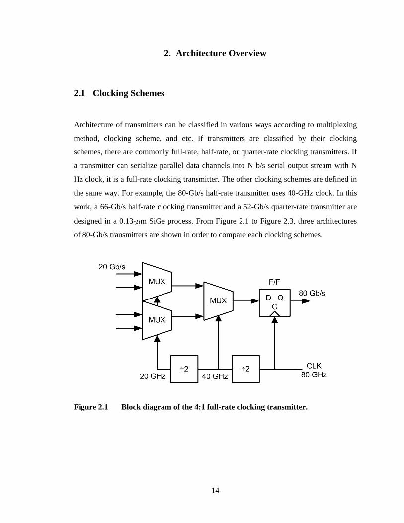
phase clocks and the 4:1 MUX architecture allows enough spare space for an LC VCO, a
cross-coupled differential LC VCO is used in the 4:1 half-rate transmitter.
Figure 2.8 Schematic diagram of differential cross-coupled LC oscillator.
The simplified schematic diagram of the cross-coupled LC VCO is shown in Figure
2.8. Two monolithic inductors in the LC VCO are implemented with a single symmetric
spiral differential inductor on the last metal layer. There are many advantages in using
the symmetric differential inductor. The differential LC VCO with the symmetric
differential inductor occupies less space than a normal one because the two separate
normal inductors are incorporated into the single symmetric differential inductor. The
electro-magnetic mismatch between two inductors decreases, too. More importantly, the
23

symmetric differential inductor has a higher Q than a conventional single-ended inductor
due to the decrease in a substrate loss effect.
The 4:1 MUX in the half-rate transmitter operates at half-rate clocking frequency.
The half-rate 4:1 MUX incorporates three 2:1 high-speed retiming MUXs (HRO-MUXs)
that are proposed in this work. The HRO-MUX incorporates High-speed Latching
Operation Flip-Flops (HLO F/Fs) for input data retiming. The HLO F/F demonstrates
25% bandwidth improvement compared with a conventional master-slave F/F. As was
pointed out earlier, the half-rate clocking scheme cannot use a final retimer, and thus it is
unavoidable that duty cycle distortions in the half-rate clock and the final 2:1 MUX are
directly transferred to the final serial output of the transmitter. In order to reduce the
duty cycle distortion, all the CML differential circuits used in the clockpath and the
datapath have symmetrical layouts. Carefully designed symmetrical layout plots are
made for the 4:1 MUX design.
Each design block is described in each corresponding chapter in much more detail.
Chapter 7 describes the cross-coupled LC VCO design, the monolithic inductor selection,
and the symmetric LC VCO design. Chapter 8 describes a high-speed latch design for
the 4:1 MUX and the comparison between the high-speed latch and a conventional latch.
Chapter 9 describes the overall design of the 4:1 half-rate transmitter. Finally, Chapter
10 shows the simulation and measurement results of the implemented 4:1 half-rate
transmitter.
24

Part II. QUARTER-RATE TRANSMITTER
25

3. Hybrid Control VCO
3.1 Introduction to VCO
A voltage-controlled oscillator (VCO) is a critical component in a communication
integrated circuit. There are various ways to design an integrated VCO. One of the
popular designs is an LC resonance circuit with a maximum frequency that could
approach the fmax of the device [21]. The LC design exhibits very good phase noise
performance due to the high quality factor Q in the resonant network. However, the LC
design requires a high quality factor Q inductor that occupies a large space on chip and
increases the cost [22]. The other problem with the LC design is that the tuning range is
usually quite limited. In contrast, a ring oscillator design is very attractive due to wide
tuning range, simplicity in design, and a small on chip die size. The ring oscillator
requires passing through multiple buffer stages, which limits the maximum frequency to
approximately fmax/10 of the device [21]. However, it provides the ring oscillator with an
intrinsic precise multi-phase clocking ability. The multi-phase clock signal generation is
important in many communication circuits such as high-speed clock recovery circuits
and binary-phase-shift-keyed (BPSK) demodulators. Multi-phase clocking is also
attractive in the design of high-speed transmitter and receiver for serial data transmission
that is in high demand with increasing high-capacity network systems such as 10-Gb/s
Ethernet and 40-Gb/s OC-768 synchronous optical network (SONET) transmission
system. An 8-phase 2.5-GHz VCO was used to sequentially latch incoming data bits in a
receiver chip for 10-Gb/s serial data transmission [23]. An 8-phase 5-GHz feedforward
interpolated VCO was used to transmit data in excess of 20-Gb/s in a serial transmitter
[24].
In this work, a VCO with an ultra wide tuning range of 12 to 23 GHz with hybrid
control schemes is presented. The VCO is a novel four-stage ring oscillator that has two
hybrid control schemes. The VCO uses feedforward interpolation topology for coarse
frequency tuning, and a varactor diode load capacitance variation for fine frequency
tuning. A buffer in the four-stage ring oscillator is designed with differential current-
26

mode logic (CML) and has differential-pair output. The VCO, therefore, has quadrature
differential-pair (8-phase) outputs. The 8-phase outputs from the 20 GHz VCO can be
used in a novel serial transmitter design to transmit data in 80 Gb/s data rate.
3.2 VCO Architecture and Hybrid Control Schemes
Figure 3.1 Block diagram of the feedforward interpolated VCO with hybrid controls.
The feedforward interpolated VCO with hybrid controls is shown in Figure 3.1. The
VCO is basically a four-stage ring oscillator with auxiliary feedforward loops to increase
the oscillation frequency. An auxiliary feedforward loop has two buffer stages while the
main loop has four buffer stages. Each buffer generates the stage n output by interpolat-
ing the L (leap) input into the P (previous) input. The L input is the stage n-2 output, and
the P input is the stage n-1 output. The feedforward interpolation topology technique is
similar to the negative skewed delay scheme [26], sub-feedback loop topology [25],
27

“leap-frog” VCO structure [23], and multiple-pass loop architecture [22]. The basic
ideas of all these methods are fundamentally same [22]. This feedforward topology in a
VCO design is popular because a simply chained ring oscillator can not achieve shorter
delay than the possible smallest delay limit. The limited minimum delay equals to the
smallest buffer delay times the number of stages. If the smallest buffer delay is τmin, the
smallest possible delay in a four-stage ring oscillator is not less than 4τmin. However, the
delay of a feedforward interpolated VCO, Tfeedforward, can be smaller than 4τmin, and
should be larger than 2τmin.
2τmin < Tfeedforward ≤ 4τmin
Therefore, the feedforward interpolation topology can achieve not only a higher
oscillation frequency but also a wider tuning range by varying the interpolation ratio.
According to Barkhausen’s criteria, an oscillator loop should have 180° phase shift
in a negative-feedback configuration. So, a conventional CMOS ring oscillator needs an
odd number of inverters, and the fastest oscillator design has a 3-stage loop. The odd
number of stages is disadvantageous because it can not generate standard quadrature
output or 8-phase output which requires even number of stages. Meanwhile, the buffer in
the feedforward interpolated VCO is designed with differential current-mode logic
(CML). In a differential logic, an even number of buffers can be used in a ring VCO
design because an inversion can be easily achieved by crossed wires without additional
delay added in the loop. The inverters in Figure 3.1 are crossed wires and don’t have any
delay except the parasitic wire delay. The phase shift of the loop in Figure 3.1 is 180°
due to the wire inversion. In this way, the ring VCO can have four stages satisfying
Barkhausen’s criteria.
The ring VCO has two hybrid schemes to control the oscillation frequency. The
VCO uses the feedforward interpolation for coarse frequency tuning, and a varactor
diode load capacitance variation for fine frequency tuning. In Figure 3.1, CV is a control
signal to vary the varactor diode load capacitance, and C31-C30 is a differential control
signal to adjust the interpolation ratio between the previous P input and the leapfrog L
input.
28

Figure 3.2 Schematic diagram for the delay buffer of the VCO.
The detailed schematic design of a delay buffer is shown in Figure 3.2. The sche-
matic design is almost identical to the FFI VCO [24] except the use of varactor diodes as
capacitance load delay. The delay buffer uses three CML levels. Top-level cascode
amplifiers are used to increase the oscillator frequency performance. The second-level
differential amplifiers take the L21-L20 input and P21-P20 input from previous stages. The
third-level differential control signals, C31−C30, changes current ratio that determines the
interpolation ratio between the L21-L20 input and the P21-P20 input. An emitter degenera-
tion resistor, Re, provides more linear frequency-voltage characteristics over a wide
tuning range.
V1 and V2 are varactor diodes which work as capacitance load affecting the oscilla-
tion frequency of the VCO. The junction capacitance of a varactor diode decreases as the
reverse voltage across it increases. Therefore, the varactor control voltage, CV, can
control the oscillation frequency by varying the capacitance in RC delay. The varactor
diode size available in the integrated circuits is limited, and the capacitance of the
varactor diode is generally in the range of a few hundred femto Farads. So, the
oscillation frequency of the VCO can be finely controlled by adjusting the CV input to
29

tion frequency of the VCO can be finely controlled by adjusting the CV input to the
varactors. Adjusting C31−C30 changes tail-current ratio in the two cascode differential
pairs, and thus the delay of the entire buffer is changed coarsely. The hybrid control
scheme can control the VCO oscillation frequency finely and coarsely with the two
control inputs, CV and C31−C30.
Figure 3.3 Simulated output waveforms of the VCO.
Figure 3.4 Simulated frequency-voltage characteristics of the VCO.
30

Figure 3.3 shows simulated waveforms of the first four phases among the eight
phases from the VCO output. Figure 3.4 shows the simulated frequency-voltage charac-
teristics of the VCO with a fixed varactor control voltage, CV, as -1 V. The simulated
frequency-voltage characteristic is very linear over the tuning range from 16.5 to 24.7 G
Hz.
Figure 3.5 Layout plot of the feedforward interpolated VCO.
Figure 3.6 Chip microphotograph of the VCO.
31
Figure 3.5 shows the layout of the VCO core with hybrid controls. The layout is
carefully designed keeping symmetry to reduce distortion in data duty cycle. The VCO
has been fabricated in a 0.13-µm SiGe-bipolar transistor technology with a 210-GHz fT.
Figure 3.6 shows the chip microphotograph of the VCO. The IC chip contains many
auxiliary circuits for testing. External control inputs, C31, C30, and CV, are internally
reduced by voltage divider circuits. D8 clock output has a frequency divide by 32 of the
VCO frequency to synchronize the VCO output, Y, with a sampling oscilloscope.
3.3 VCO Measurement Results
(a) (b)
Figure 3.7 Measured VCO output waveform at (a) 11.7 GHz and (b) 18.1 GHz.
The ring VCO IC chip is measured after fabrication in Rensselaer Polytechnic Insti-
tute. Measurements are done on die with multi-contact probes with 40-GHz bandwidth.
All testing environments are set to have 50-Ω impedance matching. Waveforms have
been measured with a digital sampling oscilloscope with 20-GHz bandwidth. Figure 3.7
shows the measured single-ended VCO output waveforms at 11.7 GHz and 18.1 GHz.
The VCO output has about 200mV peak-to-peak differential voltage swing.
32

Figure 3.8 Measured frequency-voltage characteristics varying the differential control voltage with a fixed varactor control voltage.
Figure 3.9 Measured frequency-voltage characteristics varying the varactor control voltage with a fixed differential control voltage.
33

The VCO has two hybrid control inputs, and the frequency-voltage characteristic is
measured in two ways. The external differential control input and the varactor control
input to the IC chip are internally reduced to the appropriate voltage range for the VCO
core circuit. Figure 3.8 shows the measured frequency-voltage characteristics of the
VCO varying the differential control voltage with a fixed varactor control voltage of 0
V. The coarse frequency tuning range is from 11.36 to 22.41 GHz. When a fixed varac-
tor control voltage is -3.4 V, the coarse frequency tuning range is from 11.76 to 23.26
GHz. The maximum oscillation frequency of the VCO is 23 GHz. The coarse-tuning
ratio of the VCO is about 50%. Figure 3.9 shows the measured frequency-voltage
characteristics varying the varactor control voltage with a fixed differential control
voltage set to 0 V. The fine frequency tuning range is from 17.09 to 17.41 GHz. The
fine-tuning ratio of the VCO is about 2%.
Figure 3.10 shows the power spectrum of the divide-by-32 signal of the VCO clock
when the VCO is tuned at 20 GHz. The power spectrum is measured with a FSP38
spectrum analyzer from ROHDE & SCHWARZ Co.
Figure 3.10 Measured VCO output spectrum when the VCO is tuned at 19.7 GHz.
34

Figure 3.11 Phase noise measurement when the VCO is tuned at 16.0 GHz.
Figure 3.12 Phase noise measurement when the VCO is tuned at 20.0 GHz.
35

Figure 3.11 shows the phase noise plot of the VCO tuned at 16.0 GHz. The single
sideband (SSB) phase noises at 16 GHz are –68.45 and –103.4 dBc/Hz at 100 kHz and 1
MHz offset frequency. Figure 3.12 shows the phase noise plot of the VCO tuned at 20.0
GHz. The SSB phase noises at 20 GHz are –64.73 and –104.82 dBc/Hz at 100 kHz and 1
MHz offset frequency.
Oscillation frequency 11.36 – 23.26 GHz
Coarse tuning range 50%
Fine tuning range 2%
SSB phase noise
(Center freq. 20 GHz)
-63.94 dBc/Hz @ 10kHz
-64.73 dBc/Hz @ 100kHz
-104.82 dBc/Hz @ 1MHz
Power Supply 3.4-3.8 V, 150mA
0.51 W
Chip size 1.82 mm × 0.31 mm
Technology IBM 0.13-µm SiGe BiCMOS
Figure 3.13 Ring VCO Performance summary.
Figure 3.13 shows the summary of performance for the hybrid control VCO. The
power consumption of the VCO testing chip is 0.51 W summing all additional power
consumptions in testing circuits. The 8-phase 20 GHz VCO outputs can be used as the
multi-phase clocking in the quarter-rate clocking transmitter design to transmit data up
to 80 Gb/s.
36

4. Phase-Locked Loop
A phase-locked loop (PLL) is a feedback system that compares an output phase with an
input phase, and then changes frequency of a VCO to be matched with that of a refer-
ence clock. A PLL is used in the quarter-rate transmitter to stabilize a high frequency
system clock using an external low frequency reference clock. For example, an external
625-MHz reference clock could be applied to the PLL from an external function genera-
tor to generate a 20-GHz VCO clock with a 1/32 frequency divider. The PLL for the
quarter-rate transmitter incorporates a 3-state phase-frequency detector (PFD), an RC
ladders low-pass filter (LPF), a voltage controlled oscillator (VCO), and a feedback
frequency divider. The LPF is a loop filter of the PLL.
Figure 4.1 Continuous linear model of the PLL.
Figure 4.1 shows the continuous linear model of the PLL. The PFD receives the
phase error between the reference clock and the VCO feedback clock, and produces
pulses to adjust the frequency of a VCO in response to phase errors. The PFD output
pulses should be averaged and be a slowly varying signal that is suitable for VCO
frequency control. So, a RC ladder LPF is used to filters out high-frequency components.
The VCO frequency control signal adjusts the frequency of the VCO so that the VCO
feedback frequency is matched with that of the reference clock.
37

4.1 Phase-Frequency Detector
Figure 4.2 PFD block diagram.
Figure 4.3 Input-output timing diagram of the PFD.
A phase detector (PD) has been used as a conventional method to compare phases of
two signals. The PFD is a variant of PD to improve the frequency-error detection capa-
bility. Figure 4.2 shows the schematic diagram of the PFD. The PFD is built from two
asynchronous-reset master-slave flip-flops and an AND gate. All circuits in the PFD are
current mode logic (CML) circuits. The PFD detects the phase or frequency difference
38

from the two inputs, and then produces up and down pulses to adjust the frequency of
the VCO.
The more detailed explanation for the operation of the PFD is shown in Figure 4.3.
If Vref lags Vfeed, Vdown remains high at a logical ONE. The Reset signal is generated
when both Vup and Vdown remains high. Vdown, therefore, has a pulse of which width is
linearly proportional to the phase error. Conversely, if Vref leads Vfeed, then Vup has such
a pulse. If there is no propagation delay in the circuits, the PFD has ideally three states;
only the Vup is high, only the Vdown is high, or both are low. So, this kind of PFD is
called “three-state phase detector”. But, Vup or Vdown always shows unwanted short reset
pulse due to unavoidable propagation delay. This short reset pulse could cause a small
jitter noise in the VCO clock even when the PLL is locked.
Figure 4.4 Block diagram of the Master-Slave flip-flop in the PFD.
The block diagram of the Master-Slave flip-flop (MS F/F) in the PFD is shown in
Figure 4.4. The MS F/F circuit includes two resettable latches and an intermediate buffer.
The MS F/F has a conventional design except the intermediate buffer. The intermediate
buffer is inserted to afford a timing margin between the two resettable latches. The
reference clock and the feedback clock applied to the PFD are slower by 1/32 times than
the VCO clock. This timing margin guarantees that the MS F/F will operate correctly
even with a little imprecise or slow-rising sinusoidal clock.
39

Figure 4.5 Schematic diagram of the resettable latch in the PFD.
Figure 4.5 shows the schematic diagram of the resettable latch. The resettable latch
has a differential reset input at the third CML level. The first and second CML level has
a latch configuration with a data input of ‘1’. There are two types of bipolar transistors in
the IBM 8HP SiGe-bipolar process, a high-fT bipolar transistor and a high-breakdown
transistor. A high-fT bipolar transistor is faster but less robust against breakdown, and
conversely a high-breakdown transistor is a little slower but more robust against break-
down. For higher performance, all the core circuitry in this project uses the high-fT
bipolar transistor. The collector-emitter breakdown voltage of the high-fT bipolar transis-
tor is approximately as low as double value of the base-emitter threshold voltage. To
prevent the breakdown, a diode is inserted into every high voltage CML path. A sym-
metric load resistor is adjusted to have 250-mV output voltage swing.
40

Figure 4.6 Input-output characteristics of the PFD.
Input-output characteristics of the three-state PFD is shown in Figure 4.6. The input
is the phase difference between Vref and Vfeed in Figure 4.2, and the output is the differ-
ence between the average values of Vup and Vdown in Figure 4.2. Because the PFD has
three states, the output is linear over the whole phase error range from –360° to +360°.
This input-output characteristics gives an idea of the continuous linear model of the PFD.
The continuous linear model of the PFD is a combination of a summation and a simple
linear gain KPFD as shown in Figure 4.1.
Figure 4.7 Simulated input-output waveforms of PFD.
The simulation result is shown in Figure 4.7. In the Figure, Vref is leading Vfeed, and
Vup has a pulse of which width is linearly proportional to the phase error. The PFD linear
41

gain, KPFD, is calculated to be 40m V/rad from the simulation result. The linear gain
model is used in the design of a low-pass filter transfer function, HLPF(s), so that we can
decide the low-pass filter parameters.
4.2 Low-Pass Filter
The up and down control signals shown in Figure 4.7 can not be directly applied to the
VCO because the control signal is a pulse. We need the average value of the up and
down pulses. A LPF filters out high-frequency component in the pulses and gives the
average voltage value to the VCO in order to change the VCO oscillation frequency.
Figure 4.8 Schematic diagram of the RC ladder LPF.
Figure 4.8 shows the schematic diagram of the LPF. The LPF is a two-stage RC
ladder network. A two-stage RC ladder network has two poles and has -40 dB/decade
slope in high frequency range. The two-stage RC ladder network, therefore, can have
higher high frequency signal rejection than a single-stage RC ladder network. The R and
42

C values in the LPF are decided in Matlab™ mathematical simulation described in the
following section. The continuous linear model of the LPF is HLPF.
13)(1
22 +⋅+⋅=
SRCSRCH LPF
Figure 4.9 shows the layout plot of the LPF. An emitter follower buffer follows the
LPF to match the signal voltage offset level with the VCO control input level.
Figure 4.9 Layout plot of the RC ladder LPF.
4.3 PLL Analysis and Simulation
The KPFD and KVCO in the PLL linear model shown in Figure 4.1 are generally fixed. The
KPFD is 40m [V/rad] and the KVCO is 27.5 [GHz/V]. The open-loop transfer function of
the PLL model is Hopen.
321
⋅⋅⋅= LPFVCO
PFDopen HS
KKH
13)(1
22 +⋅+⋅=
SRCSRCH LPF
43

Since the open-loop transfer function contains a pole at the origin (S = 0), the PLL
system is a type-I system that has zero steady-state error in step response. The closed-
loop transfer function of the PLL model is Hclosed.
open
openclosed H
HH
+=
1
The Hclosed is a third-order transfer function, and the pole positions should be care-
fully decided to satisfy the stability condition and to shorten the settling time that is
called “lock acquisition time” in PLL design.
Figure 4.10 Pole-locations of the PLL model.
The pole positions are decided if the R and C values in the HLPF are decided. In a
heuristic way, the R and C values are decided as 300 Ω and 3.86 pF. For the limitation in
space, the on-die capacitor should be feasibly small, and the 3.86 pF capacitor in the
44

IBM 0.13-µm SiGe process has feasible 80 µm × 48 µm size. The corresponding closed-
loop transfer function is shown below.
829318
8
102.16SS103.476 S 101.3421016.2
×++×+××
= −−closedH
The Hclosed has a unity DC gain as expected. The heuristically decided pole positions
of the PLL are plotted in Figure 4.10. All the three poles are located in the left-half s-
plane, which ensures absolute stability of the PLL system. However, it is not easy to
evaluate how stable the system is from the pole locations. Therefore, to find relative
stability, we have to do frequency analyses. Through frequency analyses, we can find
another critical parameter, loop bandwidth, too.
Figure 4.11 Bode plot of the PLL model.
45

Figure 4.12 Nyquist plot of the PLL model.
Loop bandwidth is a measure of the dynamic speed with which a PLL will lock.
Generally loops with higher loop bandwidth will lock faster, but they could be less stable.
The loop bandwidth of a PLL should be designed carefully considering many various
factors such as locking acquisition time, stability, and phase noise. Loop bandwidth is
defined in two ways, ωc and ωp. ωc is the physical loop bandwidth and is equal to be
ωn/2π, where ωn is the natural frequency of the loop. ωp is the mathematical loop band-
width and is equal to the gain-crossover frequency in which the open loop gain is equal
to 1. The natural frequency ωn of the Hclosed system is 2.647×10⁸ rad/sec, and the loop
bandwidth ωc is 42.14 MHz.
To find the mathematical loop bandwidth ωp, a Bode plot analysis is described in
Figure 4.11 with the Hopen. Bode plots are frequency-domain plots of the magnitude and
46

phase of open-loop transfer functions with s replaced by jω. The mathematical loop
bandwidth ωp is defined as the gain-crossover frequency in which the magnitude of the
open loop gain is unity. Phase margin, Φm, is the amount of margin before the closed-
loop system become unstable and is defined as the phase difference between -180° and
the phase value at ωp. ωg is the phase-crossover frequency in which the phase of the open
loop is -180°. Gain margin, Gm, is the amount of gain that is allowed to increase in the
loop before the closed-loop system become unstable and is defined to be the absolute
magnitude value at ωg. For the Hclosed system, its ωp is 29.79 MHz, and its ωg is 137.4
MHz. Its gain margin is 12, and its phase margin is 55.68°. Apparently the gain margin
and the phase margin of the Hclosed system are large enough, which confirms that the PLL
system has very good relative stability.
The Nyquist plot of the Hclosed system is shown in Figure 4.12. A Nyquist plot is
combination of the magnitude plot and the phase plot of a Bode plot, and is represented
with the magnitude and the phase in polar coordinates. A Nyquist plot is useful because
it can show the whole frequency responses in a single graph. In Figure 4.12, the phase
margin Φm and the gain-crossover frequency ωp are shown and they are identical with
the values in the Bode plot. The Nyquist locus meets the unity-circle at a point that is far
enough from the (-1, j0) point. Because the (-1, j0) point is the instability point in a
Nyquist plot, the PLL system is relatively stable enough.
The performance of the PLL can be found from the step response of the PLL linear
model. A mathematical simulation is executed in Matlab™, and shown in Figure 4.13.
The step response of the linear model has 12% overshoot at 14 n sec and 22 n sec
settling time. In order to verify the validity of the linear model and the design perform-
ance, a schematic SPICE simulation is executed and compared. Figure 4.14 shows the
step response of the PLL schematic design. The step response of the schematic design
has 19% overshoot at 13 n sec and 21 n sec settling time. Both of the simulation results
are very close. The little differences are caused in the following reasons; the PLL itself is
a discrete system, the feedback frequency divider has a temporal delay, and, above all,
all the circuits are very nonlinear. Although of the above weaknesses, the continuous
linear model of a PLL has been used for a long time due to its simplicity in design.
47

Figure 4.13 Step response of the continuous linear model of the PLL.
Figure 4.14 Step response of the schematic design of the PLL.
48

Figure 4.15 Simulated PLL locking acquisition process.
Figure 4.15 shows the process of locking acquisition in the PLL. The reference
clock is 625 MHz and applied from an external function generator. The initial feedback
clock from the VCO through the frequency divider lags far behind the 625-MHz refer-
ence clock. A corresponding large lagging phase error is detected by the PFD, and the
error signal changes rapidly the VCO frequency. The rapid change of frequency makes
an overshoot, and conversely the feedback clock leads the reference clock. This small
leading phase error slightly lowers the VCO frequency. Finally the feedback clock
frequency converges to the reference clock frequency of 625 MHz, and the PLL is
locked to make the VCO generate a stable clock output. The feedback clock has the
frequency divided by 32 from the VCO oscillation frequency, and thus the VCO fre-
quency is 20 GHz when the feedback frequency is 625 MHz.
49

Figure 4.16 PLL tracking performance simulation.
Figure 4.16 shows the frequency tracking performance of the proposed PLL. The
reference clock changes from 625 MHz to 650 MHz at 100 n sec and then to 605 MHz at
150 n sec. The feedback clock from the VCO tracks successfully the changes of the
reference clock. The corresponding VCO up and down control signal generated by the
PFD and the LPF is shown together. Whenever the PLL is locked for each step input, the
VCO control signal stays quiescent and, even better, with zero steady-state error. The
zero steady-state error in each step response is expected because the PLL system is a
type-I system. Through the PLL analyses and simulation, it is confirmed that the PLL
system is very stable and its locking ability is excellent.
4.4 PLL Measurement Results
The PLL has been fabricated in a 0.13-µm SiGe BiCMOS transistor technology with a
210-GHz fT. After fabrication, measurements are done on die with multi-contact wedge
50

probes. As shown in Figure 3.8, the frequency tuning range of the pure VCO is from 11
GHz to 22 GHz. The practical VCO tuning range in the PLL is measured from 10.2 GHz
to 20.2 GHz, which becomes a little bit slower than that of the pure VCO. It is due to the
increased driving loads in the quarter-rate transmitter because the VCO should provide
all the multi-phase clocks to the 16:1 MUX circuits.
To keep better symmetry in the layout, a direct VCO output is not connected to a
pad. Instead, the VCO feedback signal in the PLL is measured. The VCO feedback
signal has the frequency divided by 32 from the VCO frequency.
(a) (b)
Figure 4.17 Measured PLL feedback signal waveforms at (a) 350 MHz (VCO at 11.2 GHz) and (b) 630 MHz (VCO at 20.16 GHz).
The reference frequency clock to the PLL is externally supplied from a signal gen-
erator, SML01 from ROHDE & SCHWARZ Co. The PLL locking range is measured
varying the reference frequency from the signal generator. Figure 4.17 shows the meas-
ured PLL feedback signal waveform that is supplied back into the phase detector in the
PLL to compare with the reference frequency clock. The PLL has wide locking range
from 10.2 GHz to 20.2 GHz.
51

Figure 4.18 Measured 350-MHz PLL feedback output spectrum when VCO is locked at 11.2 GHz.
Figure 4.19 Measured 625-MHz PLL feedback output spectrum when VCO is locked at 20 GHz.
52

A noise performance is difficult to estimate in the time domain, and thus the power
spectrum and the phase noise of the PLL are measured with a FSP38 spectrum analyzer
from ROHDE & SCHWARZ Co. Figure 4.18 shows the output spectrum of the PLL
feedback signal when the VCO is locked at 11.2 GHz. Figure 4.19 shows the output
spectrum of the PLL feedback signal when the VCO is locked at 20 GHz. Compared
with the 20-GHz VCO output spectrum shown in Figure 3.10, the 20-GHz PLL output
spectrum shows a sharper peak at the center frequency although the span frequency
range is shorter. It means the PLL reduces much phase noise from the VCO.
Figure 4.20 PLL phase noise measurement when VCO is locked at 20 GHz.
Figure 4.20 shows the phase noise plot of the PLL output when the VCO is locked
at 20 GHz. The single sideband (SSB) phase noises are measured as –123.94 dBc/Hz at
100 kHz offset frequency and –124.64 dBc/Hz at 1 MHz offset frequency as shown in
Figure 4.20. The phase noise plot doesn’t show peaking and shows good plain linearity.
The measured phase noise incorporates the intrinsic phase noise of the signal generator
and the spectrum analyzer, however, which is hard to be separated.
53
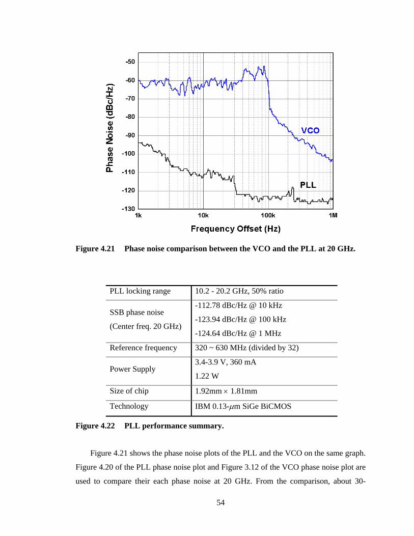
Figure 4.21 Phase noise comparison between the VCO and the PLL at 20 GHz.
PLL locking range 10.2 - 20.2 GHz, 50% ratio
SSB phase noise
(Center freq. 20 GHz)
-112.78 dBc/Hz @ 10 kHz
-123.94 dBc/Hz @ 100 kHz
-124.64 dBc/Hz @ 1 MHz
Reference frequency 320 ~ 630 MHz (divided by 32)
Power Supply 3.4-3.9 V, 360 mA
1.22 W
Size of chip 1.92mm × 1.81mm
Technology IBM 0.13-µm SiGe BiCMOS
Figure 4.22 PLL performance summary.
Figure 4.21 shows the phase noise plots of the PLL and the VCO on the same graph.
Figure 4.20 of the PLL phase noise plot and Figure 3.12 of the VCO phase noise plot are
used to compare their each phase noise at 20 GHz. From the comparison, about 30-
54

dBc/Hz phase noise is reduced by the feedback compensation in the PLL. Figure 4.22
shows the summary of performance for the PLL. The power consumption of the PLL
including the VCO is 1.22 W excluding the power consumption of testing circuits. The
multi-phase output PLL is used to drive the quarter-rate 16:1 MUX in the quarter-rate
transmitter.
55

5. 16:1 Quarter-rate Transmitter
A multiplexer is a key part in the design of a transmitter. The designed transmitter has a
16-bit parallel input and an 1-bit serial output, and thus needs a 16:1 MUX. A block
diagram of the 16:1 MUX is shown in Figure 5.1. The 16:1 MUX consists of a 16:4
MUX, Edge-Channeling 4:1 MUX, and a final cascode output amplifier.
Figure 5.1 Simplified block diagram of the 16:1 MUX circuit.
As shown in Figure 2.4, the data bit rates of the quarter-rate transmitter increase
from the beginning input stage to the final output stage. If the final serial output bit rate
is N Gb/s, the input bit rate of the 16:1 MUX is N/16 Gb/s. The output bit rate of the
16:4 MUX is N/4 Gb/s. The Edge-Channeling 4:1 MUX takes the 4-bit N/4 Gb/s data
and multiplexes them into an N Gb/s serial bit stream. The quarter-rate transmitter has a
multi-phase clocking scheme. The advantage of the multi-phase clocking scheme is that
the global clock rate doesn’t need to be as fast as the final output bit rate. As in Figure
2.4, while the final output bit rate is N Gb/s, the VCO frequency is as slow as N/4 GHz.
In practical usage, the 16 bit input data of the 16:1 MUX are provided by a chip or a
computer to transfer their data to another chip or computer through a serial transmission
56

medium. In testing, those input data should be pseudorandom bit streams (PRBS) to test
every possible data combination. The PRBS input data can be generated from an exter-
nal input data generator. But, Rensselaer Polytechnic Institute doesn’t have such
sufficiently capable and expensive equipment for testing input data generation, so the
quarter-rate transmitter needs to have a built-in on-die input data generator of a LFSR as
shown in Figure 5.1. The LFSR generates PRBS input data. The PRBS input data are 16-
bit wide. The LFSR has 31 registers to generate a 231-1 PRBS test pattern. The PRBS
test pattern is required to get the fully tested eye diagram of the quarter-rate transmitter
output. The LFSR are synchronized with a 16:4 MUX so that the 16:4 MUX can capture
the input data with the right timing. The synchronization clock between the LFSR and
the 16:4 MUX is generated from the first internal 4:1 MUX in the 16:4 MUX. Detailed
explanation of timing is described in the following section.
The 16:4 MUX has four internal 4:1 MUXs and converts the 16-bit input data into a
4-bit data streams. The Edge-Channeling 4:1 MUX takes the 4-bit data and converts
them into a serial data stream. The serial data stream contains much switching noise
ringing that is periodic and generated while passing through the Edge-Channeling 4:1
MUX. A cascode output amplifier is added to remove the ringing noise by thresholding
the serial data stream. The cascode output amplifier also provides enough gain to drive
an off-chip 50-Ω load.
5.1 16:4 MUX
The 16:4 MUX consists of four 4:1 MUXs. The 16:4 MUX is synchronized with a four
phase clock from the PLL. The four phases are 0°, 90°, 180°, and 270°. Each clock
phase is supplied to the each internal 4:1 MUX. The each internal 4:1 MUX generates a
half-frequency clock and a quarter-frequency clock of the each phase clock. For example,
if the VCO generates a 20-GHz clock, the half-frequency clock is 10 GHz, and the
quarter-frequency clock is 5 GHz. The LFSR is synchronized with the quarter-frequency
clock of the first internal 4:1 MUX to generate the 16-bit testing data pattern. The each
57

4:1 MUX processes four bits out of the sixteen bits from the LFSR. The output se-
quences of the 16:4 MUX are shown below.
MUX Output D0: D15, D11, D7, D3
MUX Output D1: D14, D10, D6, D2
MUX Output D2: D13, D9 , D5, D1
MUX Output D3: D12, D8 , D4, D0
Each sequential output stream is phase shifted by 90°, so that they will be combined
into one streaming data temporally ordered from D0 to D15 after passing through the
Edge-Channeling 4:1 MUX.
Figure 5.2 Output bit stream of the MUX Output D1 of the 16:4 MUX (D2, D6, D10 and D14 are the 16-bit data input from the LFSR).
58

Figure 5.2 shows the simulated output bit stream of the MUX Output D1 bit of the
16:4 MUX. The 4-bit input data, D2, D6, D10 and D14, from the LFSR are multiplexed
by the second internal 4:1 MUX. The VCO clock has been slowed down to 1 GHz in the
simulation to show the apparent data transition.
The 16:4 MUX design in the quarter-rate transmitter is based on that in SERDES III
Tx [19], but there are many modifications to improve its performance. In order to
describe the modifications, the timing diagram and the design of SERDES III Tx are
described ahead. Figure 5.3 shows the block diagram of an internal 4:1 MUX of the 16:4
MUX in SERDES III Tx.
Figure 5.3 Block diagram of the internal 4:1 MUX of the 16:4 MUX in SERDES III Tx.
The entire circuit design uses the CML gate logic. CML is a differential logic and
every line in the block diagram is actually a pair of differential wires. Differential gate
logic such as CML or ECL generates an inverted signal and a non-inverted signal
59

simultaneously. Therefore, the inverted clock is free from skew problems, which is the
unique advantage of differential gate logics. The main clock from the VCO is internally
divided into a half-frequency clock and then into a quarter-frequency clock. All the flip-
flops in this MUX are Master-Slave flip-flops (MS F/F). The timing diagram of this 4:1
MUX is shown in Figure 5.4.
Figure 5.4 Timing diagram of the internal 4:1 MUX of the 16:4 MUX in SERDES III Tx.
A clock signal provokes the half-frequency clock, and then the half-frequency clock
provokes the quarter-frequency clock with a short delay. All 16-bit data from the LFSR
are captured in the sixteen MS F/F of the four internal 4:1 MUXs. In each internal 4:1
MUX, the each 4 data bits are sampled by the four MS F/Fs. If the 4 data bits sampled
60

by the four MS F/Fs are Q0, Q1, Q2, and Q3 as shown in Figure 5.4, they are multi-
plexed into DA and DB using the quarter-frequency clock. The DA and DB signals are
sampled by another two MS F/Fs whose outputs are QA and QB. QA and QB are phase-
shifted by 90° of one data set period to make an interleaved serial data stream in the final
stage 2:1 MUX. The final MS F/F samples the interleaved signal DF to make the output
signal QF. In the SERDES III Tx, all the flip-flops capture their input data marginally at
the end of the valid data value. This sampling at the end could be useful in the case that a
gate delay is significantly long. In the proposed design of the internal 4:1 MUX for the
quarter-rate transmitter, most data are sampled at the center of the valid data value, and
the total transition time is shortened.
Figure 5.5 Block diagram of the internal 4:1 MUX of the 16:4 MUX in the quarter-rate transmitter.
Figure 5.5 shows the improved design of the internal 4:1 MUX in the quarter-rate
transmitter. There are two major architectural differences between the internal 4:1 MUX
61
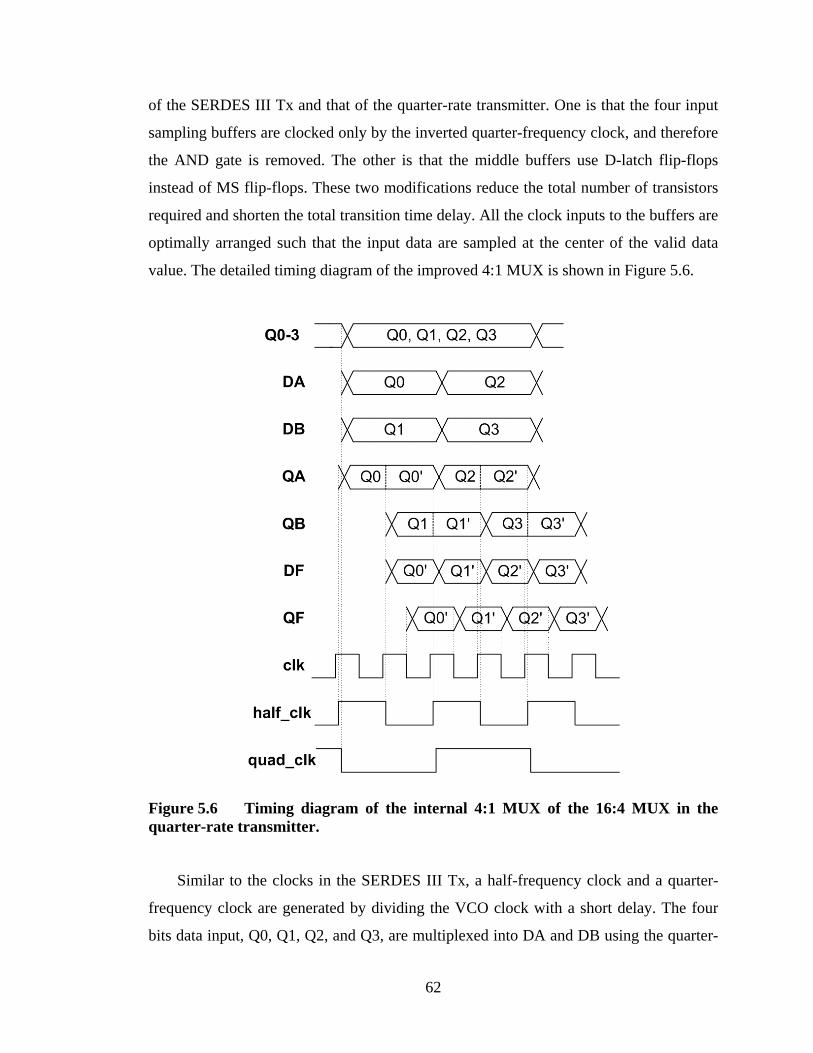
of the SERDES III Tx and that of the quarter-rate transmitter. One is that the four input
sampling buffers are clocked only by the inverted quarter-frequency clock, and therefore
the AND gate is removed. The other is that the middle buffers use D-latch flip-flops
instead of MS flip-flops. These two modifications reduce the total number of transistors
required and shorten the total transition time delay. All the clock inputs to the buffers are
optimally arranged such that the input data are sampled at the center of the valid data
value. The detailed timing diagram of the improved 4:1 MUX is shown in Figure 5.6.
Figure 5.6 Timing diagram of the internal 4:1 MUX of the 16:4 MUX in the quarter-rate transmitter.
Similar to the clocks in the SERDES III Tx, a half-frequency clock and a quarter-
frequency clock are generated by dividing the VCO clock with a short delay. The four
bits data input, Q0, Q1, Q2, and Q3, are multiplexed into DA and DB using the quarter-
62

frequency clock. Two D-latch F/Fs sample the DA and DB signals with a 90° phase-shift.
Because the middle buffers are D-latch F/Fs, Q0-Q3 indicate pass-through states, and
Q0’-Q3’ indicate latched states. The advantageous feature of the internal 4:1 MUX is
that the final 2:1 MUX takes only the stable Q0’-Q3’ latched states, and they are sam-
pled at the center of their valid data value. Therefore, the proposed internal 4:1 MUX in
the 16:4 MUX achieves better tolerance to noise and the a shorter transition time with
fewer transistors.
Figure 5.7 Schematic of the MUX-Latch in the internal 4:1 MUX.
In order to realize the timing diagram shown in Figure 5.6, the delay between the
middle 2:1 MUX and the middle D-latch F/F should be as short as possible or ideally
zero. The MUX-Latch circuit shown in Figure 5.7 is a combination of a 2:1 MUX and a
D-latch F/F. The MUX-Latch multiplexes and latches ideally at the same time, and the
proposed timing operation can be realized even at very high frequency.
63

Figure 5.8 Simulated timing diagram of the proposed internal 4:1 MUX of the 16:4 MUX in the quarter-rate transmitter.
In order to verify the performance, a simulated timing diagram is shown in Figure
5.8. The VCO clock has been slowed down to 1 GHz in this simulation to show clearly
the details of the data transitions. The middle QA D-latch F/F latches the data Q0 and Q2
bits and keeps their values as Q0(K) and Q2(K). The other middle QB D-latch F/F
latches the data Q1 and Q3 bits. The half-frequency clock switches the final 2:1 MUX,
and the falling-edge of the full-frequency clock provokes the final MS F/F to sample the
data at the center of their valid value while the middle QA and QB D-latch F/Fs are
holding their stable data states.
64

Figure 5.9 Simulated waveforms of the LFSR outputs and the 16:4 MUX sam-pled input at 6.625 Gb/s for the final serial data bit rate of 106 Gb/s.
In order to verify the high-speed operation, a full-circuit simulation including the
PLL, LFSR, and the 16:4 MUX is performed. The VCO is locked to oscillate at 26.5
GHz in the PLL. The quarter-frequency clock of the first internal 4:1 MUX is 6.625 GHz
and applied to the LFSR to generate 16-bit 6.625-Gb/s PRBS data as shown in Figure
5.9. The frequency of the quarter-frequency clock is equal to the frequency divided by
16 from the final serial data rate, and thus all the 16-bit data are generated within one
period of the quarter-rate frequency clock.
The 16-bit PRBS data generated by the LFSR are sampled in the 16:4 MUX at the
falling edge of each quarter-frequency clock as shown in Figure 5.9.
65

Figure 5.10 Simulated waveforms of the internal 4:1 MUX of the 16:4 MUX operating at 26.5 Gb/s for the final serial data bit rate of 106 Gb/s.
Figure 5.10 shows the simulated waveforms of the internal 4:1 MUX of the 16:4
MUX when the full-frequency clock from the VCO is 26.5 GHz. The internal 4:1 MUX
multiplexes the 4-bit input data successfully to generate a ‘0110’ data stream at 13.6 ns
in Figure 5.10. The output bit data rate of the internal 4:1 MUX is 26.5 Gb/s. The 4-bit
26.5-Gb/s output bit streams from the 16:4 MUX are phase-shifted by 90° with each
neighboring bit stream so that they can be multiplexed into one final serial data stream of
106-Gb/s data bit rate in the final 4:1 MUX.
66

5.2 Edge-Channeling 4:1 MUX
The final 4:1 MUX needs to use all of the 8-phase clocks from the VCO to multiplex the
4-bit input data streams that are phase-shifted by 90° with each neighboring bit stream.
The final 4:1 MUX design is based on the Edge-Channeling MUX [19]. The unique
feature of the Edge-Channeling MUX is that only the first-tier multiplexers generate all
the critical edges, and the rest of the multiplexers are used to “channel” these edges to
the output. In this way, the Edge-Channeling MUX can alleviate a duty cycle mismatch-
ing problem and have a higher bandwidth than a common 4:1 MUX architecture.
Figure 5.11 Block diagram of the Edge-Channeling 4:1 MUX and the 8-phase clocks.
67

Figure 5.11 shows the block diagram of the Edge-Channeling 4:1 MUX. W, X, Y, Z
and their complementary clocks are the 8-phase clocks from the VCO. They are phase-
shifted by 45° with each neighboring clock. All of the 8-phase clocks are used for multi-
phase multiplexing in the 4:1 MUX. X and Z clocks are delayed to match multiplexing
timing in the second-tier stage and the final stage. The Edge-Channeling 4:1 MUX
consists of seven 2:1 MUXs while a common full-rate 4:1 MUX consists of three 2:1
MUXs. The Edge-Channeling 4:1 MUX requires four more 2:1 MUXs than a common
full-rate 4:1 MUX, but the full-rate MUX needs a full-rate clock, e.g., 80 GHz for 80
Gb/s operation, while the Edge-Channeling MUX needs multi-phase 20 GHz clocks for
80 Gb/s operation.
Figure 5.12 Timing diagram of the Edge-Channeling 4:1 MUX.
68

The W, X, Y, Z and their complementary clocks appear at the top and bottom of
Figure 5.12, which show the timings when the rising edge of each clock occurs. Data
D0-D3 are the multiplexed data stream from the 16:4 MUX, and they are phase-shifted
by 90°. The 16:4 MUX uses a four-phase clock, the X, Z and their complementary
clocks, and the data D0-D3 bits have data transition at those clocks; that is, the D0
changes at the complement of the X clock, the D1 changes at the complement of the Z
clock, the D2 changes at the X clock, and the D3 changes at the Z clock.
The first-tier four MUXs generate edges in their A, B, C, and D outputs using the W
and Y clocks. Those generated edges pass through the second-tier two MUXs and the
third-tier final MUX, to be still present in the final output stream. For example, an output
signal E of a second-tier MUX has the X clock as its selection signal, but there is no data
transition at the rising edge time of the X clock. The output E signal is keeping the same
data state of the D0 without a data transition at the rising edge time of the X clock.
Although the output E signal has a data transition from D1 to D3 at the falling edge time
of the X clock, the data transition is not effective since the final 2:1 MUX with the
output G signal skips the data transition by switching and therefore this edge is not
shown in the final serial data stream. In this way, only the first-tier 2:1 MUXs generate
all the critical edges, and the other 2:1 MUXs are used to “channel” these edges to the
final serial output. Although this Edge-Channeling 4:1 MUX architecture requires more
internal 2:1 MUXs than a general 4:1 MUX design, it can alleviates a duty cycle prob-
lem and a jitter problem to the greatest extent possible [19].
However, when the Edge-Channeling MUX is used at a very high clock rate, it has a
critical drawback of “undesirable switching noise channeling”. Switching noise is
intrinsic and unavoidable in any CML multiplexer, and it is even worse in the Edge-
Channeling 4:1 MUX utilizing the no less than 8-phase clocks. Switching noise is
generated at every clock phase, transmitted intactly through “channeling”, and even
amplified through multi-layer multiplexing for the worse. This switching noise is also
transmitted through the voltage reference lines in CML circuitry. In the proposed final
4:1 multiplexer, a cascode amplifier is added after the final 2:1 multiplexer to do thresh-
olding and remove the undesirable switching noise.
69

Figure 5.13 Schematic block diagram of the Edge-Channeling 4:1 MUX.
The detailed explanation and simulation results are shown in the following sections.
The current mirror constant current source for the cascode amplifier is isolated from all
the other circuits to prevent switching noise from being transmitted through the voltage
reference line. Also, the constant current sources for the CML MUXs using different
clock phases are separated from each other to alleviate switching noise problem as
shown in Figure 5.13.
70

Figure 5.14 Layout plot of the Edge-Channeling 4:1 MUX.
Figure 5.14 shows the layout plot of the Edge-Channeling 4:1 MUX. The final 4:1
MUX must operate at the final high data rate, so its layout is designed with careful
consideration. In order to reduce an unequal duty cycle problem, all the internal 2:1
MUXs are placed symmetrically and all the differential wires have the same length. In
order to reduce undesirable parasitic effect, all the 2:1 MUXs are placed as densely as
possible and with shortest interconnection length.
71

5.3 Final Output Thresholding
The Edge-Channeling MUX shows the possibility of wider bandwidth and equal duty
cycle, but it suffers from the switching noise problem causing severe ringing at every
multi-phase clock transition as mentioned earlier.
(a) (b)
Figure 5.15 Output of the Edge-Channeling 4:1 MUX contains severe switching noise in its (a) waveform and (b) eye diagram.
(a) (b)
Figure 5.16 The final output of the quarter-rate transmitter after thresholding shows its (a) waveform and (b) eye diagram free from the switching noise problem.
Figure 5.15 (a) shows the output waveform of the Edge-Channeling 4:1 MUX at 80
Gb/s. The waveform is not flat in sequential bits with the same values, but rather it has a
periodic ringing which is caused by the multi-phase switching and channeling. The eye
diagram of Figure 5.15 (b) shows the ringing effect more clearly. An eye diagram is a
72

common tool to visualize quality of a random bit signal. An eye diagram folds so many
data bits into a certain synchronized period over a sufficiently long time, and an eye
diagram can show the accumulated data transition pattern. The wider the eye opening is,
the better quality the signal has. For example, the eye opening of Figure 5.16 (b) is wider
than that of Figure 5.15 (b), and the signal quality of Figure 5.16 (b) is better. Figure
5.16 (b) is the eye diagram of the final serial output after thresholding the output of the
Edge-Channeling 4:1 MUX. The horizontal lines at the top and bottom in Figure 5.16 (b)
are flat, which means its waveform is flat in sequential bits with the same values. In
other words, the thresholding circuit removes the periodic ringing caused by the switch-
ing noise problem. Figure 5.16 (a) shows the waveform of the final serialized output free
from the switching noise problem.
Figure 5.17 Schematic of the final 2:1 MUX and the cascode open-collector output buffer for thresholding.
Figure 5.17 shows the schematic diagram of the final 2:1 MUX in the Edge-
Channeling 4:1 MUX and the following cascode output buffer to drive off-chip 50-ohm
loads. The output buffer topology is a cascode open-collector differential pair. With the
73

off-chip 50-ohm impedances, the quarter-rate transmitter should provide a large output
current so as to produce reasonable output voltage swings. In order to get a single-ended
400-mV peak-to-peak voltage swing, the output buffer should provide 8-mA output
current for the 50-ohm impedance. Double current mirror constant current sources are
used to provide a more stable driving current. The final cascode output buffer does also
work as a thresholding circuit because a CML differential pair is basically a differential
switching circuit. The cascode configuration is a cascade of a common-emitter stage
followed by a common-base stage. The common-base stage reduces the load resistance
of the common-emitter stage, and allows the differential pair to operate at higher fre-
quencies. Another advantage of the cascode configuration is a highly increased output
resistance. The high output resistance is useful in desensitizing bias references from
variations in power-supply voltage [27]. The switching noise in the Edge-Channeling 4:1
MUX is also transmitted through a voltage reference line in a current mirror constant
current source. Therefore, the current source for the cascode buffer is isolated from all
the other circuits to prevent the ringing from being transmitted through the voltage
reference line.
74

6. Implementation and Results of 16:1 Quarter-rate Transmitter
All the IC design circuits described from Chapter 3 to Chapter 5 are integrated into the
16:1 quarter-rate transmitter. The floor plan of the complete chip is designed carefully to
place all parts as densely as possible and to keep all interconnections as symmetrical as
possible. Although it is impossible to achieve perfect symmetry for the complicated 8-
phase clockpath, best efforts are made to approach this goal. The submitted layout
design is verified with a post-layout simulation considering the resistive and capacitive
parasitic components obtained by layout parasitic extraction (LPE). Also, the submitted
layout design passes all the required design-rule checking (DRC). The fabricated chip is
tested on die with multi-contact probes. The corresponding simulation and measurement
results are described.
6.1 Implementation and Fabrication
(a) (b)
Figure 6.1 (a) The layout plot and (b) the chip microphotograph of the 16:1 quarter-rate transmitter.
75

The 16:1 quarter-rate transmitter circuit is designed utilizing the latest SiGe
BiCMOS technology, the IBM 8HP 0.13-µm SiGe process with fT 210 GHz. The de-
signed IC has a seven-level metal-layer structure. The first quarter-rate transmitter was
submitted on January 2005 for fabrication, and tested at Rensselaer Polytechnic Institute
in June 2005. The first quarter-rate transmitter is not equipped with a phase-locked loop
(PLL) due to a shortage of design time. A PLL was added in the next 8HP process
fabrication on April 2005. The second quarter-rate transmitter incorporates the ring VCO,
the PLL, the 231-1 LFSR, and the 16:1 MUX. The second quarter-rate transmitter was
tested at Rensselaer Polytechnic Institute in August 2005.
Figure 6.1 shows the layout plot and the fabricated chip microphotograph of the
second quarter-rate transmitter with the PLL. The IC chip size is approximately 1.92 mm
high by 1.81 mm wide and the chip uses about 2,700 SiGe HBTs (Heterojunction
Bipolar Transistor). In the layout design, the LFSR, the 16:4 MUX, and the 4:1 MUX
are placed in cascade considering the data-flow direction. The ring VCO is placed close
to the final 4:1 MUX because all of the full-frequency 8-phase clocks are used in the
final stage.
6.2 Power Consumption
The power supply voltage is applied from 3.4 V to 3.6 V in the measurement. The 16:1
quarter-rate transmitter consumes about 1320 mA from the power supply at 3.5 V. The
total power consumption of the fabricated transmitter chip is about 4.62 W, which is
very similar to the power consumption of 4.665 W in the post-layout simulation. In order
to estimate the partial power consumptions of each block, the power consumption in the
post-layout simulation is analyzed.
Figure 6.2 shows the total power distribution of the 16:1 quarter-rate transmitter
with a power supply voltage of 3.4 V. The total current is 1372 mA. But, the whole 16:1
quarter-rate transmitter incorporates some testing circuits, and thus those blocks should
be excluded in order to calculate the power consumption of the pure quarter-rate trans-
mitter.
76

Current (mA) Power (mW) Ratio (%)
LFSR 392 1333 29
MUX 16:4 245 833 18
MUX 4:1 130 442 9
PLL + VCO 360 1224 26
Dummy-Divider 76 258 6
I/O 169 575 12
Total 1372 mA 4665 mW 100%
Figure 6.2 Power distribution of the 16:1 quarter-rate transmitter with built-in testing circuits.
Current (mA) Power (mW) Ratio (%)
MUX 16:4 245 833 31
MUX 4:1 130 442 17
PLL + VCO 360 1224 46
I/O 50 170 6
Total 785 mA 2669 mW 100%
Figure 6.3 Power distribution of the pure 16:1 quarter-rate transmitter without the testing circuits.
Figure 6.3 shows the power distribution of the pure 16:1 quarter-rate transmitter ex-
cluding the built-in testing circuits. The power consumption of the pure quarter-rate
transmitter is no more than 2.67 W. The core 16:1 MUX block in the pure transmitter
chip consumes about 48% of the power and the clocking blocks consumes about 46% of
the power.
77

6.3 Simulation and Measurement Results
When the first quarter-rate transmitter chip design was taped out in January 2005,
Rensselaer Polytechnic Institute was equipped with only a 32-bit SPICE simulation tool.
The 32-bit SPICE tool is capable of accessing only 4 GB of system memory, which is
not enough to run the whole-chip post-layout simulation of the quarter-rate transmitter.
With this limitation of the 32-bit simulator, post-layout simulations were performed
partially on each layout subblock. A whole-chip simulation was done only with the
schematic design of the quarter-rate transmitter before fabrication. The quarter-rate
transmitter operates up to 107 Gb/s in the schematic simulation showing a wide open eye
diagram. After submission of the quarter-rate transmitter chip design, Rensselaer Poly-
technic Institute acquired a 64-bit SPICE simulator to enable the whole-chip post-layout
simulation. The whole-chip post-layout simulation result indicates that the parasitic
components effect is more serious than expected at high frequency operation as high as
40 GHz.
Figure 6.4 VCO frequency tuning in the post-layout simulation of the 16:1 quarter-rate transmitter.
78

Figure 6.4 shows the frequency tuning of the ring VCO in the post-layout simulation.
The performance of the quarter-rate transmitter can be estimated in the simulation by
tuning the VCO frequency. Although the PLL is used to tune the VCO frequency in the
actual measurement, the VCO is directly tuned in the post-layout simulation since the
PLL locking acquisition takes a long time in a post-layout simulation. The transmitter IC
has an input-pad to control the VCO tuning voltage ranging from 0 V to –3.4 V. The
corresponding tuning range of the VCO is from 12.6 to 22.3 GHz. The test inputs are the
16-bit 231-1 PRBS data generated by the internal LFSR.
Figure 6.5 Input-output waveforms of the 16:1 quarter-rate transmitter operat-ing at 54 Gb/s in a parasitic post-layout simulation.
79

Figure 6.5 shows the input-output waveforms from the pads of the transmitter IC in
the parasitic post-layout simulation. The VCO is tuned to operate at 13.5 GHz with the
control voltage at –1.5 V, thus the final serial output stream is 54 Gb/s. The LFSR output
data rate is 3.375 Gb/s that is 1/16 of the final output data rate. The LFSR reset input
signal is a –3V negative pulse. The VCO/32 has a period of 2.37 ns as expected. The
VCO/32 or VCO/16 clock signal is used to synchronize the transmitter IC with a sam-
pling oscilloscope. In order to estimate the quality of the final output waveform, the
corresponding eye diagrams are shown in Figure 6.6.
(a) X-axis: 40 ps (b) X-axis: 80 ps
Figure 6.6 54-Gb/s output eye diagrams of the 16:1 quarter-rate transmitter in a parasitic post-layout simulation.
80

(a) X-axis: 30 ps (b) X-axis: 60 ps
Figure 6.7 67.5-Gb/s output eye diagrams of the 16:1 quarter-rate transmitter in a parasitic post-layout simulation.
In Figure 6.6, the VCO generates 13.5-GHz global clocks and the final serial output
stream has a 54-Gb/s data rate in the post-layout simulation. The final serial output
stream has a wide 750-mV peak-to-peak differential voltage swing. The eye opening
voltage swing is 530 mV and the eye opening ratio is 71%. The eye crossing jitter is
about 3.87 ps.
In Figure 6.7, the VCO generates 16.87-GHz global clocks and the final serial out-
put stream has a 67.5-Gb/s data rate. The final serial output stream has a wide 770 mV
peak-to-peak differential voltage swing. The eye opening voltage swing is 538 mV and
the eye opening ratio is 70%. The eye crossing jitter is about 4.34 ps.
The simulations show more jitter and more unequal duty cycle in the 67.5-Gb/s eye
diagram than in the 54-Gb/s eye diagram. In a post-layout simulation, the eye diagram of
the quarter-rate transmitter output closes at data rates over 70 Gb/s, which means the
quarter-rate transmitter generates error signals. After analysis, it is found that the errors
occur in the final Edge-Channeling 4:1 MUX, the most high-speed part, as expected.
81

Figure 6.8 On-die measurement setup with multi-contact wedge probes.
The quarter-rate transmitter IC chip is measured after fabrication. Measurements are
done on die with multi-contact wedge probes with a 40-GHz bandwidth. The testing
environment setup is shown in Figure 6.8. All the probes, the cables, and the measure-
ment devices are set to have 50-Ω impedance matching. The output eye diagrams of the
16:1 quarter-rate transmitter are sampled using Tektronix 11801C sampling oscilloscope
with a 50-GHz bandwidth Tektronix SD-32 sampling head. The external reference clock
for the PLL is supplied from ROHDE & SCHWARZ SML01 1.1-GHz signal generator
with SSB phase noise of -122 dBc/Hz at 20 kHz offset.
82

(a) 665 MHz (b) 1 GHz
Figure 6.9 Waveforms of VCO/16 signal when the PLL is locked (a) at 10.64 GHz and (b) at 16 GHz.
(a) 2.66 Gb/s (b) 4 Gb/s
Figure 6.10 Eye diagrams of the LFSR output when the VCO is tuned (a) at 10.64 GHz and (b) at 16 GHz.
Figure 6.9 shows the measured waveforms of the VCO/16 signal from the 16:1
quarter-rate transmitter. The VCO/16 signal has the frequency divided by16 from the
VCO frequency. The ring VCO is tuned at 10.64 GHz and at 16 GHz in the PLL by
varying the reference clock frequency, and thus each corresponding VCO/16 has a
83

frequency of 665 MHz and 1 GHz. Therefore, it is confirmed that the internal divider
circuits are correctly operating. The VCO/16 signal is used as the triggering signal for
the sampling oscilloscope.
Figure 6.10 shows the measured eye diagrams of the LFSR output in the 16:1 quar-
ter-rate transmitter. The LFSR output has a wide 350-mV peak-to-peak single-ended
voltage swing. The 16-channels LFSR is tested to operate up to 4.6 Gb/s, and thus the
LFSR can provide testing data to the 16:1 quarter-rate transmitter if the transmitter
operates at less than a 73.6-Gb/s data rate.
(a) 45 Gb/s (b) 52 Gb/s
Figure 6.11 Output eye diagrams of the 16:1 quarter-rate transmitter operating (a) at 45 Gb/s and (b) at 52 Gb/s.
Figure 6.11 shows the measured single-ended output eye diagrams of the 16:1 quar-
ter-rate transmitter. Although the quarter-rate transmitter has differential outputs, only
the single-ended waveform is measured in the absence of a differential RF probe.
In Figure 6.11 (a), the PLL is locked at 11.25 GHz, and the output data rate of the
transmitter is 45 Gb/s. The 45-Gb/s eye diagram shows a wide 430-mV peak-to-peak
single-ended voltage swing, which is equal to about a 860-mV peak-to-peak differential
swing. The 45-Gb/s eye opening is single-ended 150 mV, and thus the eye opening ratio
is about 35%. The 45-Gb/s eye crossing jitter is 6.4 ps.
84

Figure 6.11 (b) shows the 52-Gb/s single-ended eye diagram of the quarter-rate
transmitter output when the PLL is locked at 13 GHz. The 52-Gb/s eye diagram shows a
wide 410-mV peak-to-peak single-ended voltage swing, which is equal to about a 820-
mV peak-to-peak differential swing. The 52-Gb/s eye opening is single-ended 130 mV,
and thus the eye opening ratio is about 32%. The 52-Gb/s eye crossing jitter is 5.8 ps.
The quarter-rate transmitter has a duty cycle of 59% at 52 Gb/s. The duty cycle mis-
matching is caused by unavoidable asymmetry in the multi-phase clockpath layout
design, which is generally one of the critical disadvantages of the multi-phase clocking
scheme.
Figure 6.12 The layout plot of the 16:1 MUX only chip incorporating pads and power rails.
Although the post-layout simulation result shows a wide open eye diagram up to
67.5-Gb/s data rate, the measured eye diagram shows eye opening up to 52 Gb/s. The
performance difference between the post-layout simulation and the measurement is 23%.
In order to investigate the cause of the performance degradation, another post-layout
simulation is performed with the 16:1 MUX only chip incorporating pads and power
85

rails. Ideal multi-phase clocks are applied to the MUX chip in the simulation. Figure
6.12 shows the layout plot of the 16:1 MUX chip. The MUX chip has the same clock-
path from the PLL to the 16:1 MUX as the quarter-rate transmitter has in order to test the
parasitic effect on the clockpath.
Figure 6.13 80-Gb/s eye diagram of the 16:1 MUX only chip in a parasitic post-layout simulation with an ideal clock source.
The 16:1 MUX chip can operate up to 84 Gb/s without eye closing in the simulation.
Figure 6.13 shows the widely open 80-Gb/s eye diagram of the 16:1 MUX only chip in
the parasitic post-layout simulation. The 80-Gb/s eye diagram shows a wide 940-mV
peak-to-peak differential voltage swing, and its eye opening is 470 mV. The eye opening
ratio is about 50%. The 80-Gb/s eye crossing jitter is 3.78 ps. As shown in Figure 6.7,
the 16:1 quarter-rate transmitter cannot operate over 70 Gb/s, while the 16:1 MUX chip
shows a wide eye opening at 80 Gb/s. The 16:1 MUX chip shows the improvement even
while incorporating the same clockpath. Consequently, the bottleneck of the quarter-rate
transmitter is the clocking source, namely the VCO and the PLL. The VCO needs larger
driving capability to supply more stable multi-phase clocks. The PLL needs more stable
locking ability to lower the phase noise of the VCO. Improvement could be achieved by
upgrading the testing equipment, too. For example, the current signal generator can
provide the reference clock up to 1.1 GHz, and thus at least 1/32 frequency divider needs
86
to be used to design a 20-GHz PLL for the 80-Gb/s quarter-rate transmitter. If a higher
frequency signal generator is available with a lower or at least same phase noise level, it
is possible to use a lower divisor number in the frequency divider. Therefore, the phase
noise of the VCO can be lowered by the PLL due to the reduced delay in the frequency
divider. The 16:1 MUX is the core block of the 16:1 quarter-rate transmitter and the
quarter-rate transmitter with better clocks is expected to operate at a higher data rate.
87

Part III. HALF-RATE TRANSMITTER
88

7. LC VCO
7.1 Cross-coupled LC VCO
An integrated LC oscillators has been a common clocking blocks in the modern RF IC
design and the high-speed digital IC design due to its good phase noise performance and
simple architecture. A high-speed serial transmitter working at two-digit Gb/s data rate is
very sensitive to the phase noise generated from a clock source, therefore an LC oscilla-
tor can be one of the best choices as a clock source. An LC oscillator can also provide a
larger output voltage swing than a ring oscillator. Because a ring oscillator consists of a
chain of buffers, the output swing of a ring oscillator cannot exceed the swing of a buffer.
Considering that a delay buffer in a ring oscillator should drive the other same size delay
buffer and a clocking buffer to drive main circuitry, the swing of a ring oscillator could
become smaller. Meanwhile, an LC oscillator is based on a resonant oscillation of a RLC
tank circuit. At a resonance frequency, a RLC tank reduces to virtually a simple resistor,
and the amplitude of its swing depends on the resistor value and a tail current value.
Thus, the swing of an LC oscillator can be designed to be large to some extent, and if
properly designed, the output peak-to-peak swing can be larger than even Vcc [31].
However, such a wonderful LC oscillator has two fundamental problems. A low phase-
noise LC oscillator needs a high quality factor Q inductor that occupies a large space on
a chip. The other problem is a limited tuning range of its oscillation frequency. Most of
LC VCO designs use a reverse biased varactor diode as a controllable capacitor. Such an
integrated varactor diode has a limited capacitance tuning range. And furthermore, at
two-digit GHz frequency, parasitic capacitances play more significant role in the RLC
tank than the varactor diode [30].
Although of the limited tuning range, an LC VCO has been frequently used to de-
sign a high-speed serial transmitter with a fixed transmission data rate due to its
significantly lower phase noise than a ring VCO. For example, a 12.5-GHz differential
LC VCO with cross-coupled topology was used to provide a full-rate system clock with
0.4-ps rms jitter for a 12.5-Gb/s serial transmitter [2]. A 20-GHz CMOS LC VCO with
89

quadrature phase outputs was used to provide a half-rate system clock for a 40-Gb/s
CMU and CDR operation [5]. A 10-GHz cross-coupled LC VCO with pMOS varactors
for 10% tuning range was used to drive a 16:1 multiplexer in a 0.25-µm SiGe BiCMOS
technology [29]. A quadrature-coupled LC VCO provides in-phase and quadrature
clocks to a 40-Gb/s 16:1 multiplexer that satisfies the OC-768 jitter generation specifica-
tion with 7 dB of margin [9].
In this work, a 40-GHz cross-coupled LC VCO is used in the design of the 4:1 half-
rate transmitter to provide differential 40-GHz clocks to a LFSR and a 4:1 multiplexer.
Figure 7.1 Schematic diagram of a cross-coupled LC VCO.
Figure 7.1 shows the simplified schematic diagram of a cross-coupled LC VCO,
which is one of the most popular topologies in the design of a differential LC oscillator.
A good explanation on oscillation is Barkhausen’s criteria. It means that if the loop gain
of a negative feedback system is equal to unity and the phase shift around the loop is
180°, the feedback system could oscillate. An LC oscillator has a frequency-selection
90

network, e.g., an LC tank, in a loop. The LC tank can stabilize the oscillation frequency
for its resonance property. To understand the principle of a cross-coupled LC VCO, an
alternative explanation on oscillation can be provided. That is the concept of “negative
resistance”.
Figure 7.2 The small-signal model of the cross-coupled LC oscillator showing negative input resistance.
At first, we should calculate the input resistance of the cross-coupled LC oscillator
seen from the LC tank. Figure 7.2 shows the small-signal model of the cross-coupled
oscillator without the LC tank. To calculate the input resistance, an 1A current source is
applied. With Kirchhoff’s current law, those following relationships are calculated.
1 = gm⋅V2 + V1/r1
1= -gm⋅V1 – V2/r2
Vin = V1 – V2
If r1 and r2 are large enough, V2 and –V1 are equal to 1/gm. Therefore, Vin is equal to
-2/gm. The input resistance seen from the LC tank is equal to Vin because we applied the
1A current source. Therefore, the input resistance Rin is equal to -2/gm. Meanwhile, if we
91

merge two RLC tanks into one equivalent tank in Figure 7.1, the equivalent parallel
resistance of the tank is 2Rp. The total equivalent resistance of the circuit is the parallel
of 2Rp and -2/gm. Thus, if it is satisfied that 1/gm ≤ Rp, the circuit can be viewed as a RLC
tank with a negative resistance. If a resistance in a RLC tank is equal to zero or negative,
the RLC tank will oscillate infinitely in response to an impulse signal or a small noise
pulse. This is the reason why a crossed-coupled LC VCO is called a “negative-Gm
oscillator”.
In Figure 7.1, Rp usually stems from the limited Q of the inductors. Cp is a com-
bined capacitance that consists of a load capacitance from an output buffer, a total
capacitance from two bipolar transistors, Q1 and Q2, and a distributed parasitic capaci-
tance from the inductors and wires. In order to control the oscillation frequency, a
varactor diode capacitance is added to the Cp in an LC VCO. However, as an on-chip
varactor diode size is limited, all other capacitances play a more dominant role in the
decision of the oscillation frequency. As told earlier, it is one of the major reasons why
an LC VCO has a limited tuning range.
7.2 Inductor Design
Figure 7.3 Physical shape of a monolithic inductor.
92

An inductor plays a critical role in the design of an LC VCO, and an inductor should be
chosen carefully. The typical measure of inductors’ performance is Quality factor, Q,
which is defined as the peak energy stored per cycle divided by the average power
dissipated per cycle for a reactive element with real losses [32]. From a simple calcula-
tion, Q is defined to be equal to ω0/β where ω0 is the resonant frequency and β is the
bandwidth of a RLC tank. Therefore, an LC VCO with a higher Q inductor will have
sharper frequency selectivity, and thus a lower phase noise.
There are a lot of factors to decide the Q value and the inductance value of an induc-
tor. Various combinations of line width, outer dimension, number of turns, and line-line
spacing determines the Q values of inductors even though they have the same amount of
inductance. Figure 7.3 shows a physical layout of a monolithic inductor. Lw is the line
width and Ls is the line-line spacing of an inductor. The outer dimension is the whole
width or length of an inductor.
Figure 7.4 Peak Q frequency vs. inductance for various outer dimensions in the IBM 0.13-µm SiGe process.
93

The line width Lw should be sufficiently wide so that the dc resistance of the induc-
tor does not limit the Q of the inductor [31]. The last layer, analog metal (AM), is used
to make the coil of a monolithic inductor in the IBM 0.13-µm SiGe process. The line-
line spacing Ls is typically chosen as the available minimum to increase Q. The mini-
mum Ls is 3 µm in the IBM 0.13-µm SiGe process, and so this length of Ls is used to
design the 40-GHz LC VCO. The outer dimension and the number of turns of the
inductor are the most critical factor to decide the inductance value. They are generally
decided according to the necessary inductance value in each application.
A monolithic inductor doesn’t have flat Q with a varying operation frequency due to
its nonideality. A peak Q frequency of an inductor is defined to be the frequency at
which the inductor has the maximum Q value. Therefore, in the design of an LC oscilla-
tor, the peak Q frequency of the inductor should be designed to be as close as possible to
the oscillation frequency of the LC oscillator to have a higher Q value.
Figure 7.4 shows the relationship between the peak Q frequency and inductance
with the change of the outer dimension in the IBM 0.13-µm SiGe process. Its Lw is
fixed as 5 µm and Ls is chosen as the minimum spacing, 3 µm, in the IBM design
process. Its number of turns is one. From Figure 7.4, it can be seen that the peak Q
frequency is approximately inversely proportional to inductance. This trend is matched
with the fact that smaller inductors are generally used at a higher frequency application
and vice versa.
In order to design a 40-GHz LC oscillator, about 240-pH inductor is the good choice
to have the peak Q frequency at 40 GHz. However, there is a limit in choosing the outer
dimension of a monolithic inductor. The minimum outer dimension of an inductor in the
IBM 0.13-µm SiGe process is 100 µm, of which the inductance is approximately 400 pH.
Therefore, we have to adjust Lw to get a lower inductance for the 40-GHz LC oscillator.
Figure 7.5 shows variations in inductance and the peak Q frequency when Lw is
changed with the fixed Ls as 3 µm and the fixed outer dimension as 100 µm. Compared
with Figure 7.4, the relationship between the peak Q frequency and inductance is no
more linear when Lw is changed. Various inductors with various sizes of Lw are applied
to design the 40-GHz cross-coupled LC VCO, and Lw is chosen as 15 µm from a
94

simulation. The Lw of 15 µm is the best choice to get the highest peak Q frequency
while keeping 40-GHz oscillation frequency. The inductance with Lw as 15 µm is 198
pH.
Figure 7.5 Dependence of inductance and peak Q frequency on line width.
In the IBM 0.13-µm SiGe process, a groundplane is available under an inductor to
reduce substrate losses. Two serious losses in a monolithic inductor arise from between
an inductor and a substrate. The first loss is caused by the capacitance between the
inductor and the substrate. When the potential between the inductor and the substrate
varies with time, the displacement current generated in the capacitance flows through the
substrate resistance and causes a loss [31]. The second loss is caused by the magnetic
coupling between the inductor and the substrate. According to Len’s law, when the
current through the inductor varies with time, an opposite-direction current is induced
through the substrate by the change of a magnetic filed. This is fundamentally the same
phenomenon observed in a transformer. In order to reduce these substrate losses, a
conductive shield can be placed under the inductor. Such a conductive shield is called a
95

groundplane in the IBM 0.13-µm SiGe process. Figure 7.6 shows the layout plot of the
40-GHz cross-coupled LC oscillator. The groundplane is the mesh underneath the
inductor.
Figure 7.6 Layout plot of the 40-GHz cross-coupled LC VCO.
There exist two possible groundplane layers in the IBM 0.13-µm SiGe process, M1
and DT. DT (Deep Trench) groundplane inductors have an opening in the p-well under-
neath the inductor to increase the resistivity of the substrate underneath the inductor with
a mesh of deep trench in the region devoid of p-well, while M1 (Metal layer 1) ground-
plane inductors have a low impedance M1 comb shaped groundplane underneath them
96
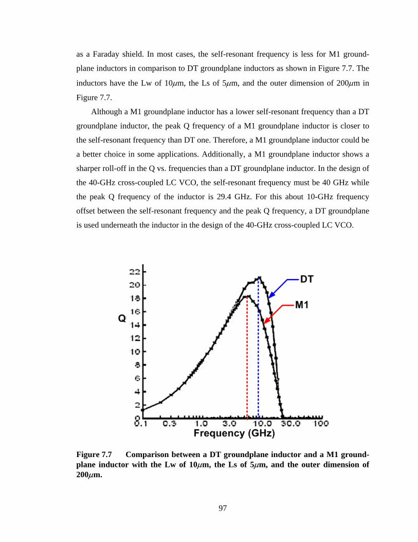
as a Faraday shield. In most cases, the self-resonant frequency is less for M1 ground-
plane inductors in comparison to DT groundplane inductors as shown in Figure 7.7. The
inductors have the Lw of 10µm, the Ls of 5µm, and the outer dimension of 200µm in
Figure 7.7.
Although a M1 groundplane inductor has a lower self-resonant frequency than a DT
groundplane inductor, the peak Q frequency of a M1 groundplane inductor is closer to
the self-resonant frequency than DT one. Therefore, a M1 groundplane inductor could be
a better choice in some applications. Additionally, a M1 groundplane inductor shows a
sharper roll-off in the Q vs. frequencies than a DT groundplane inductor. In the design of
the 40-GHz cross-coupled LC VCO, the self-resonant frequency must be 40 GHz while
the peak Q frequency of the inductor is 29.4 GHz. For this about 10-GHz frequency
offset between the self-resonant frequency and the peak Q frequency, a DT groundplane
is used underneath the inductor in the design of the 40-GHz cross-coupled LC VCO.
Figure 7.7 Comparison between a DT groundplane inductor and a M1 ground-plane inductor with the Lw of 10µm, the Ls of 5µm, and the outer dimension of 200µm.
97

Figure 7.8 DT groundplane inductors and substrate contacts placements.
In the physical layout of the DT groundplane inductors, substrate contacts must be
placed far away enough from the DT groundplane inductors. If substrate contacts are
placed closer than 50 µm, Q values of those inductors are reduced. All the DT ground-
plane inductors are placed 100 µm away from substrate contacts in the layout design of
the transmitter as shown in Figure 7.8.
As a summary of the inductor, the parameters of the 198-pH inductor in the design
of the 40-GHz cross-coupled LC VCO are decided as Lw of 15 µm, Ls of 3 µm, outer
dimension of 100 µm, 1 turn, and a DT groundplane. The final layout design of the 40-
GHz LC VCO for the transmitter is shown in Figure 7.6.
7.3 Symmetric Inductor Design
Monolithic inductors are commonly used in a single-ended configuration. As shown in
Figure 7.1, one terminal of the inductor is connected to a signal source and the other end
is connected to the ground. An interesting variation of a monolithic inductor is a sym-
98

metric inductor. Both the ends of a symmetric inductor are connected to differential
signal sources. The first 4:1 half-rate transmitter was designed with the double single-
ended inductors as shown in Figure 7.1 because a symmetric inductor device was not
available in the early version of the IBM 0.13-µm SiGe process. A symmetric inductor
device was added later in 2006, and the second 4:1 half-rate transmitter is designed with
a symmetric inductor.
Figure 7.9 Layout plot of the 40-GHz symmetric cross-coupled LC VCO.
Figure 7.9 shows the layout plot of the cross-coupled LC VCO with a symmetric in-
ductor. While the normal cross-coupled LC VCO in Figure 7.6 has double single-ended
spiral inductors, the LC VCO in Figure 7.9 has a single symmetric spiral inductor. The
crossover point in the symmetric inductor structure is implemented with a metal layer
underneath the inductor coil layer. At a glance, it can be easily found that the symmetric
99

cross-coupled LC VCO occupies a less area than the normal one. Additionally, because
two separate inductors are incorporated into a single inductor, an electro-magnetic
mismatch between the two inductors decreases.
More importantly, the symmetric inductor has a higher Q than the single-ended in-
ductor [33]. The small-signal analyses are described in the following figures.
Figure 7.10 Single-ended excitation model of a monolithic spiral inductor.
Figure 7.11 Differential excitation model of a monolithic symmetric inductor.
100

While Figure 7.10 shows a small-signal model of a spiral inductor excited by a sin-
gle-ended source with the other end connected to the ground, Figure 7.11 shows a small-
signal model of a symmetric inductor excited by differential sources. The substrate
resistance at the single-ended configuration is R, while it doubles to be 2R at the differ-
ential configuration because the symmetric inductor is driven differentially at the both
ends. At high frequency, the substrate parasitics, R and C, play a considerable role.
The substrate resistance appears in parallel with the inductor, therefore the increase
in the substrate resistance diminishes the effect of substrate loss. Therefore, the Q of the
differential symmetric inductor improves.
Figure 7.12 Schematic diagram of the 40-GHz symmetric cross-coupled LC VCO.
As shown above, a symmetric inductor has a lot of advantages over a normal induc-
tor if used in differential configuration. The second version of the 4:1 half-rate
transmitter is designed with the symmetric cross-coupled LC VCO. The schematic
101

diagram of the VCO is shown in Figure 7.12. The symmetric cross-coupled LC VCO
incorporates varactor diodes, CV1 and CV2, in order to tune the oscillation frequency. As
mentioned earlier, however, the tuning rage is narrow due to the limit of a monolithic
varactor diode. The corresponding layout plot of the symmetric cross-coupled LC VCO
is shown in Figure 7.9.
102

8. High Speed Latch
A latch and a Flip-Flop (F/F) are fundamental design components to decide the operating
bandwidth of the transmitter system. Considering the relationship between a F/F data
rate and a transistor’s fT or fmax, it is reported that a typical master-slave F/F (MS F/F)
can operate at the data rate of one-fifth the transistor’s fT for FET transistors and one-
fourth the transistor’s fmax for BJT transistors [38]. In order to overcome the bandwidth
limitation of a typical MS F/F, various novel designs have been proposed. Among a lot
of various novel F/Fs, the High-speed Latching Operation Flip-Flop (HLO F/F) devel-
oped at NTT LSI Laboratories is used to improve the transmission data rate of the 4:1
half-rate transmitter.
8.1 High-speed Latching Operation Flip-Flop (HLO F/F)
HLO F/F is known to operate about 30% faster than a conventional MS F/F [36]. Al-
though there might exist a little bit faster F/F, HLO F/F is very attractive for the reasons
that HLO F/F uses the same number of transistors used in a conventional MS F/F and the
architecture of HLO F/F is as simple as that of a conventional MS F/F. Architectural
simplicity is critical in the design of very high-speed differential circuit because simplic-
ity leads to symmetry easily. A layout mismatch in a symmetric differential circuit will
cause a duty cycle mismatch in its differential signal. Besides, the more complicated a
circuit is, the longer the internal interconnections are. As a transistor’s fT increases over a
two-digit GHz frequency, interconnection parasitics are known to play a more and more
important role in the decision of the bandwidth of a circuit.
HLO F/F has two different features compared with a conventional MS F/F, asym-
metric transistor sizes and optimized tail-currents. Figure 8.1 shows the schematic
diagram of an asymmetric D-latch that is one of the higher-speed latches than a conven-
tional D-latch. The topological configuration of an asymmetric D-latch is identical with
that of a conventional D-latch, but the transistors’ sizes of the holding circuit are smaller
than those of the reading circuit. The smaller transistor’s size leads to the less input
103

capacitance of the holding circuit. Therefore, the holding state time becomes shorter than
the reading state time. Consequently the total delay time in the latching circuit can be
reduced. This improvement is possible because the positive feedback at the holding part
can be only strong enough to make “weak” regeneration that can hold the state.
Figure 8.1 Schematic diagram of an asymmetric latch.
An asymmetric D-latch is very useful and handy because it has the same simple ar-
chitecture as a conventional D-latch. However an asymmetric D-latch has a drawback of
difficulty in choosing the tail-current value. As shown in Figure 8.2, each size of transis-
tors has its specific collector current value to achieve the maximum fT. However, all
transistors of an asymmetric latch cannot have their optimum collector currents. It is
because although the transistor’s size at the reading circuit is different with that at the
holding circuit, they should share the same tail current as shown in Figure 8.1.
104

Figure 8.2 fT characteristics vs. emitter size for high-fT NPN devices in the IBM 8HP process (from the IBM BiCMOS 8HP Model Guide).
Simply we can find that if we can provide individually optimized collector currents
to each transistor, the delay of an asymmetric latch can be reduced. High-speed Latching
Operation Flip-Flop (HLO F/F) is based on this idea.
Figure 8.3 illustrates the schematic diagram of a HLO F/F. The prime difference be-
tween a HLO F/F and an asymmetric F/F is a crossed tail-current path at the second
CML level. The differential pairs of Q1-Q2 and Q5-Q6 are reading circuits while the
differential pairs of Q3-Q4 and Q7-Q8 are holding circuits. The emitter size ratio
between the reading and the holding circuits is heuristically decided to be 10/6. The
collector current for the reading transistors to achieve the maximum fT is Iss1 while the
collector current for the holding transistors is Iss2. Due to the crossed tail-current path,
Q5-Q6 pairs are biased with Iss1, and Q3-Q4 pairs are biased with Iss2.
105

Figure 8.3 Schematic diagram of a high-speed latching operation flip-flop (HLO F/F).
In this way, all the differential pairs are biased with their optimized collector cur-
rents to achieve the maximum fT. Therefore, a HLO F/F is supposed to operate at higher
frequency than a conventional MS F/F and an asymmetric F/F. Additionally, a HLO F/F
consumes about 25% less current than a conventional MS F/F because Iss2 is smaller
than Iss1 to be optimized for the smaller size transistors at the holding circuits. In the
next section, their performances are compared through a frequency divider test.
8.2 Performance Comparison
In order to evaluate the performance of a HLO F/F, a simple frequency divider is used.
A frequency divider test is commonly used when we evaluate the performances of
106

latches or flip-flops. The block diagram of a frequency divide-by-two circuit is shown in
Figure 8.4. The simple divide-by-two circuit incorporates a MS F/F with a negative
feedback. The MS F/F can respond only to either a rising edge or a falling edge of a
clock, and the stored data is updated at the half frequency of a clock frequency. Also, the
input data is the inversion of the output data of the MS F/F, and therefore the output data
of the divider is toggled periodically. Consequently, the divider can divide the frequency
of the input clock signal by two.
Figure 8.4 Flipflop-based frequency divide-by-two circuit.
To evaluate the performance of a HLO F/F, three kinds of dividers are compared.
Although they have identical topologies as shown in Figure 8.4, the each main MS F/F is
a conventional MS F/F, an asymmetric F/F, or a HLO F/F. Input clock frequency is
swept from 20 to 100 GHz.
Figure 8.5 shows the output frequency vs. the input frequency of the three kinds of
the dividers in a schematic simulation. The maximum operation frequencies of the
conventional MS F/F divider, the asymmetric F/F divider, and the HLO F/F divider are
78 GHz, 89 GHz, and 97 GHz each. The HLO F/F divider shows the highest operation
frequency as expected, and achieves about 25% improvement compared with a conven-
tional MS F/F divider. All the F/Fs in the 4:1 MUX of the half-rate transmitter are HLO
F/Fs to improve the operation data rate.
107

Figure 8.5 Frequency dividers performance comparison
8.3 Symmetrical Layout Design
A standard cell library for the design of the half-rate transmitter is developed in the IBM
SiGe 0.13-µm process. All the CML differential circuits in the standard cell library
should have layouts as symmetrical as possible to reduce the duty cycle mismatching.
Especially, the high-speed differential circuits used for the final 2:1 MUX and the 4:1
MUX need to have almost perfectly symmetrical layouts because while they are operat-
ing at the very high frequency, their layout defects are directly related with the output
signal quality. Also, all of the interconnections connecting the high-speed circuits must
be minimally shortened because interconnection parasitics are known to play more
serious role as the operation frequency increases. Needless to say, a nonsymmetrical
108

layout design will cause a mismatch of the interconnection parasitics and increase the
output jitter, too.
Figure 8.6 shows a layout plot of an asymmetric D-latch whose corresponding
schematic is shown in Figure 8.1. The layout in Figure 8.6 is simply designed imitating
the schematic configuration in Figure 8.1. The differential data path and the differential
clock path in Figure 8.6 are both nonsymmetrical. If these nonsymmetrical D-latches are
cascaded, the mismatches in the differential data path and the differential clock path are
cumulated to be large.
Figure 8.6 Nonsymmetrical layout plot of an asymmetric D-latch.
109

Figure 8.7 Symmetrical layout plot of an asymmetric D-latch.
Figure 8.7 is the symmetrical layout of the asymmetric D-latch in Figure 8.1. Com-
pared with the nonsymmetrical layout in Figure 8.6, the differential data path and the
differential clock path of the symmetrical layout are perfectly matched. Also, the input
ports and output ports of the D-latch are placed symmetrically and the cascaded D-
latches can still keep the symmetry. Additionally, the width of the symmetrical layout is
reduced by 20% compared with that of the nonsymmetrical layout. This method to keep
layout symmetry can be applied to the layout of a HLO F/F in the same way.
110

Figure 8.8 Nonsymmetrical layout plot of a HLO F/F.
Figure 8.8 shows the layout plot of a HLO F/F whose corresponding schematic is
shown in Figure 8.3. The HLO F/F layout in Figure 8.8 is almost same with the cascade
of the asymmetric D-latch layouts in Figure 8.6 except the crossed tail-current path. The
nonsymmetrical layout of the HLO F/F in Figure 8.8 has also the inherent disadvantages
of the nonsymmetrical layout of the asymmetric D-latch. In comparison, Figure 8.9
shows the symmetrical layout plot of the HLO F/F. As in the case of the symmetrical
layout of the asymmetric D-latch, the differential data path and the differential clock
path in the symmetrical layout of the HLO F/F are perfectly matched keeping symmetry.
Also, the differential data path and the differential clock path are almost straight lines
without a branch so that the HLO F/F scarcely suffers from interconnection parasitic
capacitances and resistances. The width of the symmetrical layout of the HLO F/F is
reduced compared with that of the nonsymmetrical layout, and thus it saves the chip
space and reduces the total interconnection parasitics.
111

Figure 8.9 Symmetrical layout plot of a HLO F/F.
The HLO F/Fs are critical components in the design of the half-rate 4:1 MUX. The
half-rate 4:1 MUX consists of three high-speed retiming operation 2:1 MUXs (HRO-
MUXs) that internally use the HLO F/Fs and the asymmetric D-latch for data retiming
and data alignment.
112

9. 4:1 Half-rate Transmitter
The 4:1 half-rate transmitter consists of the built-in testing circuit, the 4:1 half-rate MUX,
the output amplifier, the PLL, and the clockpath. Rensselaer Polytechnic Institute cannot
be equipped with a four-channel 20-Gb/s random data generator. Therefore, the testing
input data generation circuit needs to be built in the chip together. For the output eye-
diagram measurement, a linear feedback shifting register (LFSR) is added in the trans-
mitter chip. The LFSR can generate a pseudorandom bit stream (PRBS) data with a 4-bit
width and a 27-1 sequence. Also, a ring-counter is added in the other version of a trans-
mitter chip. A simple bit-error rate (BER) testing can be performed with a periodic data
sequence from the ring-counter. The simplified block diagram of the 4:1 half-rate
transmitter is shown in Figure 9.1.
Figure 9.1 Simplified block diagram of the 4:1 half-rate transmitter.
The 4:1 MUX operates at the half-rate clocking frequency. In the half-rate clocking
configuration, the PLL is supposed to provide a 40-GHz clock to the 4:1 MUX if the
final output data rate of the 4:1 MUX is 80 Gb/s. The half-rate 4:1 MUX incorporates
113

three 2:1 high-speed retiming MUXs (HRO-MUXs). A HRO-MUX incorporates the
HLO F/Fs shown in Figure 8.3 for input data retiming. The detailed circuitry, the timing
diagram, and the simulation results are described in the following section.
9.1 High-speed Retiming Operation 2:1 MUX (HRO-MUX)
A conventional tree architecture 4:1 MUX consists of three 2:1 MUXs. The five-latch
MUX is one of the most widely used 2:1 MUX designs [39][40]. The simplified block
diagram of the five-latch 2:1 MUX is shown in Figure 9.2. In order to save power or
space, the number of latches might be reduced to three from five [41].
Figure 9.2 Simplified block diagram of the 2:1 five-latch MUX.
The first two cascaded latches on the D0 datapath of the five-latch MUX are each
driven by a clock and its complementary clock, and thus they cooperate to be a master-
slave F/F (MS F/F) to retime the input data bit D0. There is the other same MS F/F on
the D1 datapath. The fifth latch on the D1 datapath is used to shift the channel timing by
a half-clock cycle. For example, the data channel Q2 in Figure 9.2 is offset by a half-
clock cycle in the time domain compared with the other data channel Q0. The selector
passes the channel Q0 when CLK is low while passing the other channel Q2 when CLK
is high. In order to avoid simultaneous data transitions between both the channels, one of
the data channel should be offset from the other channel by adding the fifth latch.
114

Figure 9.3 Simplified block diagram of the HRO-MUX.
Figure 9.4 Timing diagram of the HRO-MUX.
115

Figure 9.3 shows the simplified block diagram of the high-speed retiming operation
2:1 MUX (HRO-MUX). The HRO-MUX consists of two HLO F/Fs, an asymmetric
latch, and a selector. The difference between the HRO-MUX and the five-latch MUX is
the datapath. As shown in the simulation result of Figure 8.5, the maximum operation
frequency of a HLO F/F is higher than that of a conventional MS F/F or an asymmetric
F/F. Thus, if HLO F/Fs are used in the datapath, the output quality and the operation
bandwidth of a MUX can be improved. In order to provide the half-clock data offset
between both the data channels, an asymmetric latch is used because an asymmetric
latch can operate at higher frequency than a normal D-latch.
The timing diagram of the HRO-MUX shown in Figure 9.4 is identical with that of
the five-latch MUX. D0 and D1 are the input data in Figure 9.3. The input data D0 and
D1 are sampled by the HLO F/Fs at the rising edge of CLK. Those sampled Q0 and Q1
are retimed in the HLO F/Fs, and thus although the input data generator such as the
LFSR can not guarantee the exact arrivals of the input data, the timing of the input data
can be aligned with CLK. Q2 is the time-shifted data by the asymmetric latch. The
selector switches over between the two input channels. Because the two input channels
are offset to each other, the selector can switch avoiding simultaneous transitions.
Figure 9.5 Schematic diagram of the HRO-MUX.
116

Figure 9.6 Layout plot of the HRO-MUX.
Figure 9.5 shows the schematic design diagram of the HRO-MUX of which
datapath and clock-path are differentially interconnected. Its corresponding layout plot is
shown in Figure 9.6. The layout of the HRO-MUX incorporates two symmetrical layout
plots of the HLO F/Fs in Figure 8.9, and thus keeps the datapath symmetrical and short.
9.2 Tree Architecture 4:1 MUX
The 4:1 MUX is the core block of the 4:1 half-rate transmitter. The 4:1 MUX samples
the 4-bit input data and multiplexed them into a single bit stream synchronizing with the
clock from the PLL. The clock distribution from the PLL to the 4:1 MUX is shown in
Figure 9.1. The structure of the 4:1 MUX is conventional tree architecture. Figure 9.7
shows the schematic diagram of the tree architecture 4:1 MUX.
117

Figure 9.7 Schematic diagram of the tree architecture 4:1 MUX.
Figure 9.8 Layout plot of the tree architecture 4:1 MUX.
118

The tree architecture 4:1 MUX incorporates three 2:1 HRO-MUXs in Figure 9.5. If
the final output data rate is 80-Gb/s, the two HRO-MUXs at the first-tier is driven by 20-
GHz clock and the HRO-MUX at the second-tier is driven by 40-GHz clock. The
operation frequency of the first-tier HRO-MUXs is the half of the operation frequency of
the second-tier HRO-MUX. Therefore, in order to reduce the power consumption and
space, the transistors used in the first-tier HRO-MUXs can be scaled down by half with
respect to those in the second-tier HRO-MUX. Figure 9.8 is the corresponding layout
plot of the tree architecture 4:1 MUX shown in Figure 9.7.
Figure 9.9 Simulated waveforms of the tree architecture 4:1 MUX operating at 100-Gb/s.
119

In order to verify the layout design of the 4:1 MUX, a parasitic post-layout simula-
tion is done with the layout in Figure 9.8. In the post-layout simulation, a 50-GHz ideal
clock source is applied as shown in Figure 9.9. From the simulation results, two things
should be verified, the bit error rate and the eye-diagram of the output signal. In order to
check the bit-error rate (BER), the 27-1 LFSR provides the 4-bit wide PRBS input
sequence to the 4:1 MUX. All the 27-1 random sequential data are tested on the 4:1
MUX to show zero BER in the simulation.
Figure 9.10 Simulated eye diagram of the tree architecture 4:1 MUX operating at 100-Gb/s.
Figure 9.9 shows the waveforms from the post-layout simulation on the tree archi-
tecture 4:1 MUX. The applied clock is ideal 50-GHz and the input data are 25-Gb/s
PRBS data. For example, the 4-bit input data pattern is ‘1110’ at 7.83 ns and the multi-
plexed output stream from the 4:1 MUX is correctly matched.
The quality of the output stream is confirmed in the simulated eye diagram shown in
Figure 9.10. The eye opening is almost fully opened and the data-dependent jitter is very
low. In order to verify the symmetry in the layout in Figure 9.8, four eyes are displayed.
There is little difference between these eyes, if any, which verifies the symmetry of the
120

layout of the 4:1 MUX. It confirms that the symmetrical layout designs of the HLO F/F
and the HRO-MUX are very effective.
9.3 Built-in Testing Circuit
For the lack of the high-speed testing equipment, some testing circuits need to be built
on the die itself. The 4:1 half-rate transmitter incorporates three built-in testing circuits, a
synchronization clock generator for a sampling oscilloscope, a 27-1 LFSR, and a ring
counter.
The synchronization clock generator is a simple frequency divider to provide a static
slow sampling clock for a sampling oscilloscope. Most high-speed oscilloscopes are
sampling oscilloscopes, and they require such an external synchronization clock. The
frequency divider is set to divide by 64 to generate 625-MHz for the sampling oscillo-
scope.
Figure 9.11 Simplified block diagram of Galois 27-1 LFSR.
A LFSR is a PRBS data generator for testing. A conventional method to design a
LFSR is using the Galois configuration or the XOR-tapped configuration. For example,
121

the LFSR polynomial to make a 7-bit LFSR is ‘x7+x+1’. The corresponding Galois 7-bit
LFSR is shown in Figure 9.11. Clock interconnections for all F/Fs are not shown, but
assumed to be all connected to a single clock. The Galois 7-bit LFSR is able to generate
a 27-1 PRBS sequence. But, the Galois LFSR can generate only one serial stream while
the 4:1 half-rate transmitter needs a 4-bit wide input data at one time. The simplest
solution is making four separate Galois LFSRs to generate the 4-bit PRBS data, however,
it is a waste of space and power. Instead, if a state machine can generate the same Galois
PRBS sequences by four bits at one time, the multiplexed serial stream of the 4-bit
streams will be identical to the single Galois PRBS stream. Such a configuration for a
multi-bit output LFSR is based on the ‘advance-by-16’ LFSR design [19].
Figure 9.12 Simplified block diagram of the 27-1 LFSR with a 4-bit output.
The simplified block diagram of the 27-1 LFSR with a 4-bit output is shown in
Figure 9.12. Clock interconnections for all F/Fs are not shown, but assumed to be all
122

connected to a single clock again. Compared with the Galois 7-bits LFSR in Figure 9.11,
the 27-1 LFSR with a 4-bit output in Figure 9.12 has four XOR gates for the simultane-
ous state transition by 4-bit at each clock cycle. The LFSR polynomial equation is
modified to provide the 4-bit jumping at each clock cycle. The D6 bit F/F is equipped
with an external reset in case that all the F/Fs have initial zero states. The all-zero state
seems to rarely happen. In a real measurement condition, however, this external reset is
indispensable because all the F/Fs are stubbornly willing to stay the zero states with a
slowly increasing power supply voltage that is required to protect a vulnerable IC die.
Figure 9.13 The layout plot of the 27-1 LFSR with 4-bit output.
Figure 9.13 shows the corresponding layout plot of the 27-1 LFSR with a 4-bit out-
put. The output ports of the LFSR are aligned with the input ports of the 4:1 MUX to
keep symmetry and reduce interconnection parasitics.
The other testing input circuit is a ring counter for a simple BER test. In order to
perform a full BER test on a serial transmitter, at least a serial receiver operating at the
same data rate is required. But, the 4:1 half-rate transmitter is a state-of-the-art design,
and thus the matched serial receiver is not available. Although a full BER test with a
long PRBS cannot be performed, a simple BER test can be done with a short period of
deterministic signal. A ring counter is a good example to generate such a short period of
deterministic signal.
123

Figure 9.14 Block diagram of the Johnson ring counter for a simple BER test.
Figure 9.15 The output data pattern of the Johnson ring counter.
124

Figure 9.14 shows the block diagram of a ring counter used in the 4:1 half-rate
transmitter for its simple BER test. The type of the counter is the 3-bit Johnson ring
counter with the negative feedback input. All the three registers are clocked simultane-
ously. The 4-bit input data for the 4:1 half-rate transmitter are generated from the 3-bit
state of the ring counter while considering the DC-balance of the data pattern.
Figure 9.15 is the data sequence table of the 4-bit output data pattern from the John-
son ring counter. As shown in the table, any bit stream of the data can be used as a
triggering clock signal for a sampling oscilloscope because the period of a stream signal
is equal to the period of the ring counter. The D3 stream is used as the external trigger-
ing signal through some frequency divider circuits. From the table, the DC-balance can
be easily confirmed by counting the numbers of zero and one. Both of the numbers of
zero and one are equal, and thus the data pattern is dc-balanced.
Figure 9.16 The layout plot of the Johnson ring counter for simple BER test.
125

Figure 9.16 shows the layout plot of the Johnson ring counter for the simple BER
test. For an 80-Gb/s serial transmission, 20-Gb/s test input signals should be generated
for the 4:1 MUX. In order to ensure such a high-speed operation of the ring counter,
HLO F/Fs are used as the internal registers in the ring counter.
9.4 Doubly-terminated Output Amplifier
Figure 9.17 Schematic diagram of the doubly-terminated output amplifier.
An output amplifier amplifies the serial output stream from the 4:1 MUX to drive an
external 50-Ω impedance load. The output amplifier in the quarter-rate transmitter is a
cascode open-collector amplifier shown in Figure 5.17. An open-collector amplifier is
advantageous in providing a large output swing because the amplifier should drive an
external load only. However, at very high frequency, the open-collector amplifier is
126

going to suffer from the power reflection in a transmission line although the length of the
transmission line is short. The 4:1 half-rate transmitter aims at achieving a higher data
rate than the quarter-rate transmitter, and thus the output amplifier of the half-rate
transmitter is doubly-terminated.
In a measurement, all the external interconnections and equipments are set to have
50-Ω impedance, for example, a 50-Ω microprobes, 50-Ω coaxial RF cables, and a 50-Ω
sampling head. Therefore, the characteristic impedance of transmission lines is 50 Ω,
and the output amplifier has a 50 Ω resistor as shown in Figure 9.17. Since the driven
load seen from the transistor’s collector is the parallel impedance of 25 Ω, the doubly-
terminated output amplifier has the half output swing of the open-collector amplifier
with the same amount of a tail current.
A cascode amplifier configuration requires a third CML level signal for its input at
high frequency. In order to be a third CML level signal, a first CML level signal from a
common buffer needs to pass through two emitter followers. Such a third CML level
signal shows a more distortion than a second CML level signal. In order to reduce the
input signal distortion, the doubly-terminated output amplifier uses a simple differential
amplifier configuration rather than the cascode amplifier configuration, and thus the
input CML level is the second one showing a small distortion.
127

10. Implementation and Results of the 4:1 Half-rate Transmitter
All of the IC design components described from Chapter 7 to Chapter 9 are integrated
into the 4:1 half-rate transmitter IC chip that is fabricated in MOSIS, which is a low-cost
prototyping and small-volume production service for VLSI circuit development. The
fabricated IC chips are tested on die in Rensselaer Polytechnic Institute. The related
post-layout simulation results and the measurement results are followed.
10.1 Implementation and Fabrication
(a) (b)
Figure 10.1 (a) The layout plot and (b) the chip microphotograph of the 4:1 half-rate transmitter with the PLL and the LC VCO.
The 4:1 half-rate transmitter is fabricated in the IBM 0.13-µm SiGe BiCMOS technol-
ogy. Seven metal layers are used. The monolithic inductor is built on the last metal layer.
The half-rate transmitter incorporates the cross-coupled LC VCO, the PLL, the tree
architecture 4:1 MUX, the 27-1 LFSR, and the 3-bit Johnson ring counter. Two versions
of the 4:1 half-rate transmitter are implemented for various testing purposes. The first
128

version incorporates the PLL and the LC VCO as the clocking source. The other version
incorporates the 3-bit Johnson ring counter for the simple BER test and an external clock
input pad to test the half-rate transmitter at various data rates.
Figure 10.1 shows the layout plot and the chip microphotograph of the first version
of the half-rate transmitter with the PLL and the LC VCO clocking source. The chip size
of the first version transmitter is 2000 um by 1800 um, and the chip uses about 950 SiGe
HBTs (Heterojunction Bipolar Transistors).
(a) (b)
Figure 10.2 (a) The layout plot and (b) the chip microphotograph of the 4:1 half-rate transmitter with the ring counter and the external clock input pad.
Figure 10.2 shows the layout plot and the chip microphotograph of the second ver-
sion of the half-rate transmitter incorporating both of the built-in testing circuits, the 27-1
LFSR and the 3-bit Johnson ring counter. The chip size of the second version transmitter
is 2000 um by 2000 um, and the chip used about 850 SiGe HBTs. In the design layouts,
empty chip spaces are filled with some purposive filling components, although not
shown in the layout plots for a better visuality, to satisfy a required pattern density rule
defined in the IBM design kits. In some empty spaces, some bypass capacitors are
placed to reduce power supply noise. Those bypass capacitors are connected from the
supply voltage line to the power supply return (ground).
129

10.2 Power Consumption
Power supply voltage is applied from 3.4 V to 3.9 V in the measurement. The 4:1 half-
rate transmitter with the LFSR consumes about 450 mA at the power supply of 3.5 V.
The total power consumption of the fabricated chip is about 1.575 W, which is very
similar to the power consumption of 1.448 W in the post-layout simulation.
Current (mA) Power (mW) Ratio (%)
LFSR 118 401 28
MUX 4:1 88 299 21
LC VCO 31 105 7
Clock Path 88 299 21
Divider 39 133 9
I/O 62 211 15
Total 426 mA 1448 mW 100%
Figure 10.3 Power distribution in the 4:1 half-rate transmitter with the built-in testing circuits.
Current (mA) Power (mW) Ratio (%)
MUX 4:1 88 299 39
LC VCO 31 105 14
Clock Path 88 299 39
I/O 20 68 9
Total 227 mA 772 mW 100%
Figure 10.4 Power distribution of the pure 4:1 half-rate transmitter without the testing circuits.
130

In order to estimate the partial power consumptions of each block, the power
consumption in the post-layout simulation is analyzed. Figure 10.3 shows the total
power distribution in the 4:1 half-rate transmitter with the power supply voltage of 3.4 V.
The total current flowed is 426 mA.
However, the 4:1 half-rate transmitter incorporates some testing circuits, and thus
those blocks must be excluded in order to calculate the power consumption of the pure
transmitter itself. For example, the power consumption of the LFSR is 401 mW, and it is
much higher than the power consumption, 299 mW, of the core 4:1 MUX. Figure 10.4
shows the power distribution of the pure 4:1 half-rate transmitter excluding those testing
circuits. The power consumption of the pure half-rate transmitter is only 0.77 W. The
state of the art of the 4:1 MUX IC chip from IBM consumes about 1.45W [43], and
comparatively the 0.77 W power consumption of the half-rate transmitter is very low
even considering the fact that the half-rate transmitter incorporates the CMU block. The
core 4:1 MUX block in the pure transmitter chip consumes about 39% of the total
power. The clocking block consisting of the LC VCO and the clock path consumes about
53% of the total power. More than half power is consumed for the clocking because the
transmitter is operating at very high frequency.
10.3 Transmitter Simulation
In order to evaluate the final performance of the transmitter and estimate the parasitic
effect, post-layout simulations are done. Resistive and capacitive parasitic components
on the interconnections and the devices are considered.
Figure 10.5 shows the eye diagrams in the post-layout simulations. In the simula-
tions, an external clock drives the 4:1 half-rate transmitter through the external clock pad
at various frequencies from 35 GHz to 50 GHz. The output eye diagram of the transmit-
ter comes to degenerate over 90 Gb/s, but shows a wide eye opening at the data rate of
80 Gb/s. The transmitter is capable to operate even at 90 Gb/s although its eye opening is
a little bit narrower.
131

(a) 70 Gb/s (b) 80 Gb/s
(a) 90 Gb/s (b) 100 Gb/s
Figure 10.5 Eye diagrams of the 4:1 half-rate transmitter driven by an external clock at various frequencies in post-layout simulations.
Therefore, it is confirmed that the entire transmitter’s circuits except the clock gen-
erator is designed adequately to make the half-rate transmitter operate at 80 Gb/s. The
other post-layout simulation is done to verify the design of the transmitter with the
internal clock generator.
Figure 10.6 shows the output eye diagram in the post-layout simulation. In this post-
layout simulation, the half-rate transmitter is driven by the internal 40.5-GHz LC VCO
to serialize 4-bit 20.25-Gb/s PRBS inputs from the 27-1 LFSR. The final serial output
stream has an 81-Gb/s data rate with a wide 800-mV peak-to-peak differential voltage
swing. The eye opening voltage swing is 440-mV and the eye opening ratio is 55%.
Figure 10.6 shows the double eye diagrams to verify the symmetry of the half-rate
transmitter layout design. The double eyes are almost identical showing a duty cycle of
almost 50%, and thus it confirms the overall symmetry in the layout design.
132

Figure 10.6 81-Gb/s eye diagrams of the 4:1 half-rate transmitter with the built-in LC VCO in a post-layout simulation.
Figure 10.7 80-Gb/s half-eye diagram of the 4:1 half-rate transmitter with the Johnson ring counter input pattern in a post-layout simulation.
133

Another post-layout simulation is done on the half-rate transmitter with the Johnson
ring counter to run a simple BER test. Figure 10.7 shows the periodic output waveform
of the 4:1 half-rate transmitter. The half-rate transmitter is driven by the internal 40-GHz
LC VCO to serialize the periodic 4-bit 20-Gb/s input data from the Johnson ring counter
of which the data pattern is listed in Figure 9.15. The serialized output stream is matched
with the data pattern of Figure 9.15, and thus the simple BER test verifies the correct
operation of the 4:1 half-rate transmitter. The long serialized output stream has the 24-bit
sequence that is difficult to be sampled at once on a sampling oscilloscope. Considering
the limit of the sampling oscilloscope, the output stream pattern is folded in time domain
such as an eye diagram to display the special half-eye pattern in Figure 10.7.
10.4 Transmitter with Cables and Probes Simulation
Figure 10.8 Cable attenuation.
In order to perform a more realistic simulation, a transmission line cable model and a
probe circuit model are included in the transmitter simulation. In the transmission line
cable model, its propagation velocity, physical length, characteristic impedance, capaci-
134

tance per unit length, resistance loss per unit length, and conductance loss per unit length
need to be decided. Some of those parameters are correlated. From a cable specification
and calculation, the parameters are decided as 50-Ω characteristic impedance, 0.695
propagation velocity factor, 96.46-pF/m capacitance, 79.32-Ω/m resistance loss, and 1.6-
mMho/m conductance loss. The cable length is varied for various simulations.
Figure 10.8 shows the comparison between the measured cable attenuation and the
simulated cable attenuation. They are well matched, and thus the transmission line cable
model is verified.
Figure 10.9 50-GHz probe circuit model.
Figure 10.9 shows the simple first-order low-pass probe circuit model with the
bandwidth of 50 GHz. The resistance loss is estimated from the probe length and the
cable transmission model. The capacitance is decided considering the bandwidth of the
probe. Figure 10.10 shows the AC frequency response of the probe model to verify the
50-GHz bandwidth of the probe.
A more realistic post-layout simulation is performed including those transmission
line cable models and probe model. No need to say that resistive and capacitive parasitic
components inside the chip are extracted and included, too. In order to test the transmit-
ter’s performance at various frequencies, an external single-ended clock is applied to the
transmitter through the transmission line cable model and the probe model. The internal
27-1 LFSR supplies the 4-bit testing data.
135

Figure 10.10 Probe AC frequency response.
Figure 10.11 80-Gb/s eye diagram with a 8 inches cable.
136

Figure 10.12 80-Gb/s eye diagram with a 12 inches cable.
Figure 10.13 80-Gb/s eye diagram with a 20 inches cable.
Figure 10.14 80-Gb/s eye diagram with a 30 inches cable.
137
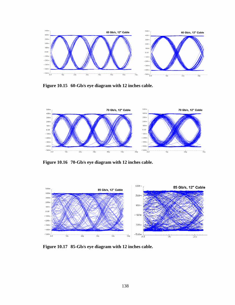
Figure 10.15 60-Gb/s eye diagram with 12 inches cable.
Figure 10.16 70-Gb/s eye diagram with 12 inches cable.
Figure 10.17 85-Gb/s eye diagram with 12 inches cable.
138

Figure 10.11 - Figure 10.14 show 80-Gb/s eye diagrams with various lengths of ca-
bles, 8, 12, 20, and 30 inches. As expected, the 80-Gb/s eye diagram with the shortest 8
inches cable shows the widest eye opening of a differential 440 mV. The 80-Gb/s eye
diagram with the 30 inches cable is almost closed.
Other simulations are performed with a fixed length of the cable. Figure 10.15 -
Figure 10.17 and Figure 10.12 show eye diagrams with a 12 inches long cable at various
data rates, 60, 70, 80, and 85-Gb/s. As expected again, the slowest 60-Gb/s eye diagram
with a 12 inches cable shows the widest eye opening of a differential 725 mV. The 85-
Gb/s eye diagram with a 12 inches cable is closed.
Cable length 60 Gb/s 70 Gb/s 80 Gb/s 85 Gb/s
8″ cable Open Open Open Closed
12″ cable Open Open Open Closed
20″ cable Open Open Open Closed
30″ cable Open Open Closed Closed
Figure 10.18 Eye opening summary according to cable lengths and data rates.
Figure 10.18 shows the summary of eye openings at various lengths of a cable and
various data rates. From the simulation, it is found that a no longer than 20 inches cable
is required to measure an 80-Gb/s eye diagram from the half-rate transmitter. However,
in the real measurement environment, the signal generator, the probe, and the sampling
oscilloscope are not as ideal as in the simulations. Therefore, it is supposed to have a
margin enough to compensate for such a physical nonideality.
139

10.5 Measurement Results
Actual measurements are done on the fabricated die with 50-GHz bandwidth multi-
contact wedge probes from GGB Industries, Inc. All the probes and cables are set to
have 50-Ω impedance matching. The serial output stream of the 4:1 half-rate transmitter
is sampled by Tektronix 11801C sampling oscilloscope with a 50-GHz bandwidth
Tektronix SD-32 sampling head. The external clock is applied by Anritsu 68369A 40-
GHz signal generator with SSB phase noise -94 dBc/Hz at 100 kHz offset.
Figure 10.19 Comparison of the data sequences in the simulation and the meas-urement.
The 4-bit wide test input data are generated by the internal Johnson ring counter. As
mentioned above, if the clock frequency goes too high, the full-length sequence cannot
be sampled at once on a sampling oscilloscope. The 24-bit full sequence output is
sampled by 40 Gb/s. Figure 10.19 shows the measured serialized output stream whose
sequence pattern is matched with the simulated pattern and also with the data pattern
table in Figure 9.15. It verifies the validity of the measured output sequences.
140

Figure 10.20 40-Gb/s waveform of the 4:1 half-rate transmitter.
Figure 10.21 50-Gb/s waveform of the 4:1 half-rate transmitter.
141

Figure 10.22 60-Gb/s waveform of the 4:1 half-rate transmitter.
Figure 10.23 66-Gb/s waveform of the 4:1 half-rate transmitter.
Figure 10.20 − Figure 10.23 show the single-ended half-eye output diagrams of the
4:1 half-rate transmitter driven by the external clock. The test input data are the 4-bit
parallel data supplied from the on-die Johnson ring counter. Although the actual output
of the half-rate transmitter is differential, only the single-ended output from one output
pad is measured for the restriction of the sampling oscilloscope. The measured single-
ended output sequence patterns are matched with the output sequence pattern in the post-
142

layout simulation shown in Figure 10.7. Therefore, it is confirmed that the 4:1 half-rate
transmitter operates correctly and the BER is very low if any. Without a high-speed
multi-channel BER testing equipment, it is impossible to measure the exact BER.
Figure 10.24 Measured RMS jitter of 831-fs on the 4:1 half-rate transmitter operating at 60-Gb/s.
In the measurement, the maximum operation data rate of the 4:1 half-rate transmit-
ter is 66 Gb/s. At 60-Gb/s data rate, the output of the transmitter has a 110-mV peak-to-
peak single-ended voltage swing while driving a 50-Ω impedance external load, which is
equal to a 220-mV peak-to-peak differential voltage swing. The output peak-to-peak
differential voltage swing in the post-layout simulation is 800 mV. There is 72% signal
power attenuation through the probes, the cables, and the oscilloscope. The attenuation is
due to the limited bandwidth of those testing equipments. The bandwidths of the probes
and the oscilloscope are 50 GHz. The bandwidth of the cables is even only 40 GHz.
143

Conventionally in order to measure such a high data rate as 60 Gb/s, very high-speed
equipments with a triple or at least double frequencies, 60 GHz, bandwidth need to be
used. In this limited testing environment, such a high attenuation rate is unavoidable.
Also, the double termination in the output amplifier reduces the output swing, too. The
double termination, however, reduces the output jitter increased by signal interference
caused by reflections in the transmission lines. The 60-Gb/s eye opening swing of the
output is a single-ended 60 mV and the eye opening ratio is 54.5%, which is very close
to 55% ratio in the post-layout simulation. The eye crossing jitter is about 2.9 ps. The
half-rate transmitter has a good duty cycle of 53% at 60 Gb/s for the symmetrical layout
design. Figure 10.24 shows the measured signal histogram of the single-ended output
from the 4:1 half-rate transmitter operating at 60-Gb/s. The measured RMS jitter is as
low as 831-fs.
144

Part IV. CONCLUSION
145
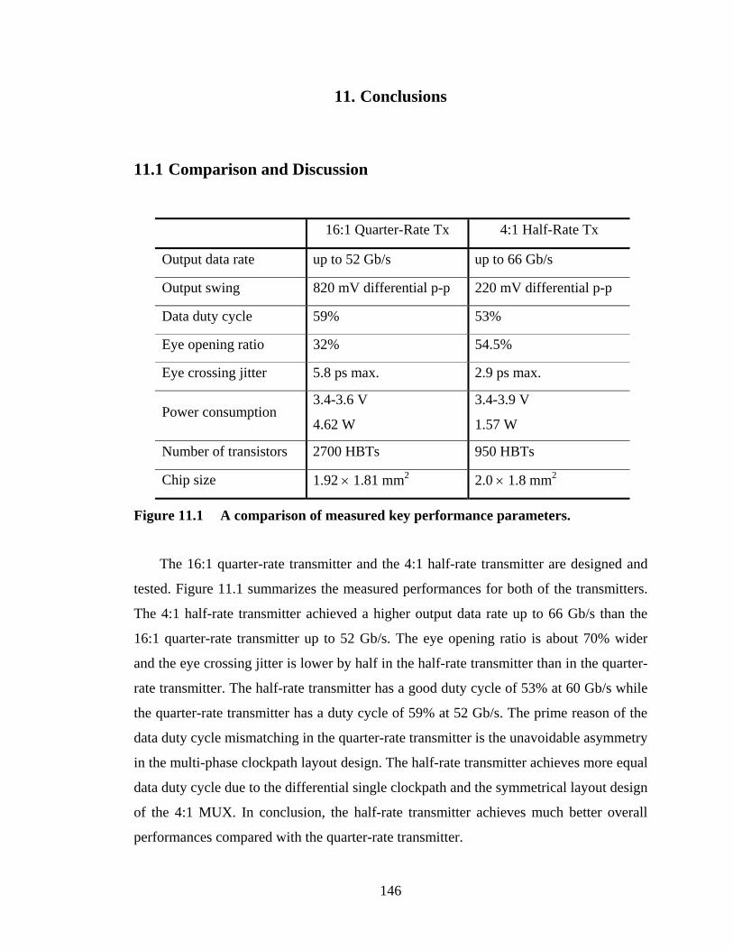
11. Conclusions
11.1 Comparison and Discussion
16:1 Quarter-Rate Tx 4:1 Half-Rate Tx
Output data rate up to 52 Gb/s up to 66 Gb/s
Output swing 820 mV differential p-p 220 mV differential p-p
Data duty cycle 59% 53%
Eye opening ratio 32% 54.5%
Eye crossing jitter 5.8 ps max. 2.9 ps max.
Power consumption 3.4-3.6 V
4.62 W
3.4-3.9 V
1.57 W
Number of transistors 2700 HBTs 950 HBTs
Chip size 1.92 × 1.81 mm2 2.0 × 1.8 mm2
Figure 11.1 A comparison of measured key performance parameters.
The 16:1 quarter-rate transmitter and the 4:1 half-rate transmitter are designed and
tested. Figure 11.1 summarizes the measured performances for both of the transmitters.
The 4:1 half-rate transmitter achieved a higher output data rate up to 66 Gb/s than the
16:1 quarter-rate transmitter up to 52 Gb/s. The eye opening ratio is about 70% wider
and the eye crossing jitter is lower by half in the half-rate transmitter than in the quarter-
rate transmitter. The half-rate transmitter has a good duty cycle of 53% at 60 Gb/s while
the quarter-rate transmitter has a duty cycle of 59% at 52 Gb/s. The prime reason of the
data duty cycle mismatching in the quarter-rate transmitter is the unavoidable asymmetry
in the multi-phase clockpath layout design. The half-rate transmitter achieves more equal
data duty cycle due to the differential single clockpath and the symmetrical layout design
of the 4:1 MUX. In conclusion, the half-rate transmitter achieves much better overall
performances compared with the quarter-rate transmitter.
146

On the other hand, the output swing of the quarter-rate transmitter is much larger
than that of the half-rate transmitter because the quarter-rate transmitter amplifies its
output through the cascode open-collector output amplifier while the half-rate transmit-
ter amplifies through the doubly-terminated output amplifier. As expected, however, the
half-rate transmitter with the doubly-terminated output amplifier shows a wider band-
width and a less jitter noise. Therefore, there is a trade-off between the output swing and
the output quality in the output amplifier.
Both of the transmitters are designed to use a negative 3.4 V power supply because
the CML logic circuits in the transmitters use the three CML levels. The power con-
sumption of the 16:1 quarter-rate transmitter is about three times more than that of the
4:1 half-rate transmitter. This is natural because the quarter-rate transmitter has the 16:1
MUX and the 16-bit 231-1 LFSR while the half-rate transmitter has the 4:1 MUX and the
4-bit 27-1 LFSR. Also, the quarter-rate transmitter uses about three times more HBTs
than the half-rate transmitter, which is matched with the power consumption ratio.
Pure 4:1 Quarter-Rate Tx Pure 4:1 Half-Rate Tx
4:1 MUX 442 mW 299 mW
CMU 1224 mW 404 mW
I/O 170 mW 68 mW
Total 1.84 W 0.77 W
Figure 11.2 Comparison of power distributions between a pure 4:1 quarter-rate transmitter and a pure 4:1 half-rate transmitter.
In other reported 4:1 transmitters, the power consumptions of the state of the art are
1.61 W [11] and 4.9 W [8]. Although the proposed 4:1 half-rate transmitter incorporates
the LFSR for test data generation, it achieves a lower power consumption of 1.57 W.
The proposed 4:1 half-rate transmitter without the LFSR consumes no more than 0.77 W.
Therefore, the proposed 4:1 half-rate transmitter design achieves the less power con-
sumption than the state of the art.
In order to compare under equal conditions, power consumptions of pure 4:1 trans-
mitter configurations in each clocking scheme are compared. As shown in Figure 11.2,
147

the pure 4:1 half-rate transmitter consumes less power than the pure 4:1 quarter-rate
transmitter. One of the reasons is the Edge-Channeling 4:1 MUX in the quarter-rate
transmitter. Although the Edge-Channeling 4:1 MUX is a novel design with multi-phase
clocking multiplexing, the Edge-Channeling 4:1 MUX requires seven 2:1 MUXs while a
conventional tree architecture 4:1 MUX requires only three 2:1 MUXs. The other reason
is the multi-phase CMU in the quarter-rate transmitter. The multi-phase CMU requires a
ring oscillator with four stages and as many driving buffers. Therefore, if power con-
sumption is a major consideration in some applications, the half-rate clocking scheme is
a better choice than the quarter-rate clocking scheme.
Speed Process Ratio Power Clocking
T. Krawczyk (RPI) 16:1
20Gb/s
0.5µm SiGe
fT 50GHz 40.0 % 3.3V
Quarter-rate
clock
Vitesse Co. 16:1
40Gb/s
InP,
fT 150GHz 26.7 % 5.2V, 3.6W Full-rate clock
Big Bear Co. 4:1
43Gb/s
0.18µm SiGe
fT 120GHz 35.8 % 5.2V, 4.8W Half-rate clock
Hitachi 16:1
43Gb/s
0.18µm SiGe,
fT 140GHz 30.7 % 1.8V, 11.6W Full-rate clock
IBM 4:1
43Gb/s
0.18µm SiGe
fT 120GHz 35.8 % 3.6V, 2.3W Full-rate clock
16:1 Tx (Yim, RPI) 16:1
52Gb/s
0.13µm SiGe
fT 210GHz 24.8 % 3.4V, 2.7W
Quarter-rate
clock
4:1 Tx (Yim, RPI) 4:1
66Gb/s
0.13µm SiGe
fT 210GHz 31.4 % 3.4V, 0.77W Half-rate clock
Figure 11.3 Comparison with the state of the art designs.
Figure 11.3 shows the performance and specification comparison between the state
of the art designs and this work. Both of the transmitters achieve higher data rates than
the state of the art while consuming less power. Considering the data rate vs. fT ratio, the
4:1 half-rate transmitter achieved a better ratio than the two state of the art designs.
148

11.2 Conclusion and Future Work
In conclusion, various novel integrated circuits for high-speed serial data transmission
are designed utilizing the latest 0.13-µm SiGe BiCMOS technology. A feedforward
interpolated voltage-controlled ring oscillator with varactor diodes demonstrates the ultra
wide tuning range of 12 to 23 GHz with the hybrid control schemes of coarse frequency
tuning and fine frequency tuning. The ring VCO has 8-phase clocks for the 16:1 quarter-
rate transmitter. A third-order PLL is designed and implemented, and a continuous
model for the PLL is developed and analyzed. The PLL has wide locking range from
10.2 GHz to 20.2 GHz with low phase noise of -123.94 dBc/Hz at 100 kHz offset. About
30-dBc/Hz phase noise is reduced by the feedback compensation in the PLL compared
with the VCO phase noise. A symmetric cross-coupled LC VCO with a high Q is
designed and used for the 4:1 half-rate transmitter. A novel high-speed F/F, HLO F/F, is
designed and compared with conventional designs. A symmetric high-speed 4:1 MUX is
designed with the newly proposed HRO-MUXs. The HRO-MUX achieves bandwidth
improvement due to its high-speed data retiming.
By grouping and utilizing all the various technologies, two different clocking ap-
proaches, including a quarter-rate clocking and a half-rate clocking, are made to design
transmitters. A 16:1 quarter-rate transmitter and a 4:1 half-rate transmitter are designed
and tested. Their performances and power consumptions are compared and analyzed.
As future work, another possible clocking scheme in transmitter design is a full-rate
clocking. Although a full-rate clocking transmitter and a half-rate clocking transmitter
are already compared [11], all the three clocking schemes have not been compared yet in
the same technology. Inductor peaking technique is not tried in this work for the re-
straints of the chip space and the power consumption. A 4:1 MUX design with frequent
usages of inductor peaking requires about 3.5 times more space and 8 times more power
[39] than the proposed 4:1 half-rate transmitter in this work. However, the inductor
peaking is a promising technique to increase bandwidths of most circuits.
149

LITERATURE CITED
[1] J. M. Khoury and K. R. Lakshmikumar, “High-speed serial transceivers for data
communication systems,” IEEE Communications Magazine, vol. 39, no. 7, pp.
160-165, July 2001.
[2] D. Friedman, M. Meghelli, B. Parker, H. Ainspan and M. Soyuer, “Sub-
Picosecond Jitter SiGe BiCMOS Transmit and Receive PLLs for 12.5 Gbaud
Serial Data,” IEEE Symposium on VLSI Circuits Digest of Technical Papers,
June 2000, pp. 132–135.
[3] C. Ridgeway and H. Sangha, “Making the move to serial buses,” EDN, Feb.
2005.
[4] T. S. Brown, M. J. Gilson, and M. G. Mason, “Synchronisation in data net-
works,” BT Technology Journal, vol. 16, no. 1, pp. 159-170, Jan., 1998.
[5] D. J. Friedman et al., “SiGe BiCMOS integrated circuits for high-speed serial
communication links,” IBM J. RES. & DEV. vol. 47, no. 2/3, pp. 259-282,
Mar/May 2003.
[6] M. Fukaishi et al., “A 20-Gb/s CMOS multichannel transmitter and re-ceiver
chip set for ultra-high-resolution digital displays,” IEEE J. Solid-State Circuits,
vol. 35, no. 11, pp. 1611–1618, Nov. 2000.
[7] K. Watanabe, A. Koyama, T. Harada, T. Aida, A. Ito, T. Murata, H. Yoshioka,
M. Sonehara, H. Yamashita, K. Ishikawa, M. Ito, N. Shiramizu, T. Nakamura,
K. Ohhata, F. Arakawa, T. Kususnoki, H. Chiba, T. Kurihara, and M. Kuraiashi,
“A low-jitter 16:1 MUX and a high-sensitivity 1:16 DEMUX with integrated
39.8 to 43 GHz VCO for OC-768 communication systems,” IEEE Int. Solid-
State Circuits Conf. Dig. Tech. Papers, Feb. 2004, pp. 166-167.
[8] D. K. Shaeffer, H. Tao, Q. Lee, A. Ong, V. Condito, S. Benyamin, W. Wong, X.
Si, S. Kudszus, and M. Tarsia, “A 40/43Gb/s SONET OC-768 SiGe 4:1
MUX/CMU,” IEEE Int. Solid-State Circuits Conf. Dig. Tech. Papers, 2003, pp.
236-237.
150

[9] Hai Tao et al., “40–43-Gb/s OC-768 16:1 MUX/CMU chipset with SFI-5 com-
pliance,” IEEE J. Solid-State Circuits, vol. 38, no. 12, pp. 2169-2180, Dec.
2003.
[10] M. Meghelli, A. Rylyakov, S. Zier, M. Sorna, and D. Friedman, “A 0.18-µm
SiGe BiCMOS receiver and transmitter chipset for SONET OC-768 transmis-
sion systems,” IEEE J. Solid-State Circuits, vol. 38, no. 12, pp. 2147-2154, Dec.
2003.
[11] M. Meghelli, “A 43-Gb/s full-rate clock transmitter in 0.18-µm SiGe BiCMOS
technology,” IEEE J. Solid-State Circuits, vol. 40, no. 10, pp. 2046-2050, Oct.
2005.
[12] H. Partovi, et al., “A 62.5Gb/s multi-standard SerDes IC,” Custom Integrated
Circuits Conf., Sep. 2003, pp. 585-588.
[13] C. Lee, T. Yao, A. Mangan, K. Yau, M. A. Copeland, and S. P. Voinigescu,
“SiGe BiCMOS 65-GHz BPSK Transmitter and 30 to 122 GHz LC-varactor
VCOs with up to 21% Tuning Range,” Proc. IEEE Compound Semiconductor
Integrated Circuit Symposium, Oct. 2004, pp. 179-182.
[14] R. Liu et al., “A 63 GHz VCO using a standard 0.25-µm CMOS process,”
IEEE Int. Solid-State Circuits Conf. Dig. Tech. Papers, 2004, pp. 446-447.
[15] M. Bao , Y. Li and H. Jacobsson, “A 21.5/43-GHz dual-frequency balanced
colpitts VCO in SiGe technology,” IEEE J. Solid-State Circuits, vol. 39, no. 8,
pp. 1352-1355, Aug. 2004.
[16] J. Kim, J.O. Plouchart, N. Zamdmer, R. Trzcinski, K. Wu, B.J. Gross, and M.
Kim, “A 44 GHz differentially tuned VCO with 4 GHz tuning range in 0.12-µm
SOI CMOS,” IEEE In. Solid-State Circuits Conf., Feb. 2005, pp. 416–417.
[17] G. Raybon, P. J. Winzer, and C. R. Doerr, “10 x 107-Gbit/s electronically
multiplexed and optically equalized NRZ transmission over 400 km,” PDP32 in
Proc OFC2006, Anaheim, CA, 2006.
[18] A. Liu et al, “A high-speed silicon optical modulator based on a metal-oxide-
semiconductor capacitor,” Nature, vol. 427, pp. 615-618, Feb. 2004.
[19] P. F. Curran, “Circuits for the realization of high speed serial transmitters us-
ing SiGe HBTs, ” Thesis in Rensselaer Polytechnic Institute, August 2005.
151

[20] Y. U. Yim, J. F. McDonald, and R. P. Kraft, “12-23 GHz Ultra Wide Tuning
Range Voltage-Controlled Ring Oscillator with Hybrid Control Schemes,” Proc.
of IEEE Annual Symposium on VLSI (ISVLSI), May 2005, pp. 278-279.
[21] A.W. Buchwald and K.W. Martin, “High-speed voltage-controlled oscillator
with quadrature outputs,” Electron. Lett., vol.27, no.4, pp.309-310, Feb. 1991.
[22] Y. Eken and J. Uyemura, “A 5.9 GHz voltage-controlled ring oscillator in
0.18-µm CMOS,” IEEE J. Solid-State Circuits, vol. 39, pp. 230-233, Jan. 2004.
[23] R.C. Walker, K. Hsieh, T.A. Knotts, and C. Yen, “A 10Gb/s Si-bipolar TX/RX
chipset for computer data transmission,” Proc. IEEE Int. Solid-State Circuits
Conf., 1998, pp. 302-303.
[24] T. W. Krawczyk, P. F. Curran, M. W. Ernest, S. A. Steidl, S. R. Carlough, J. F.
McDonald, and R. P. Kraft, “SiGe HBT Serial transmitter architecture for high
speed variable bit rate intercomputer networking,” Proc. IEE Circuit Devices
Syst., vol. 151, no. 4, Aug. 2004.
[25] L. Sun, T. Kwasniewski, and K. Iniewski, “A quadrature output voltage con-
trolled ring oscillator based on three-stage subfeedback loops,” Proc. Int. Symp.
Circuits and Systems, vol. 2, Orlando, FL, 1999, pp. 176-179.
[26] S.-J. Lee, B. Kim, and K. Lee, “A novel high-speed ring oscillator for multi-
phase clock generation using negative skewed-delay scheme,” IEEE J. Solid-
State Circuits, vol. 32, pp. 289-291, Feb. 1997.
[27] P. R. Gray, P. J. Hurst, S. H. Lewis, and R. G. Meyer, “Analysis and design of
analog integrated circuits,” John Wiley & Sons, Inc. Fourth Edition.
[28] A. S. Sedra and K. C. Smith, “Microelectronic Circuits,” Saunders College
Publishing, Second Edition.
[29] H.–I. Cong et al., “A 10-Gb/s 16:1 multiplexer and 10-GHz clock synthesizer
in 0.25-µm SiGe BICMOS,” IEEE J. Solid-State Circuits, vol. 36, no. 12, pp.
1946–1953, Dec. 2001.
[30] B. Razavi, “RF Microelectronics,” Upper Saddle River, NJ: Prentice-Hall.
[31] B. Razavi, “Design of integrated circuits for optical communications,”
McGraw-Hill Companies Inc.
152
[32] J. W. Nilsson, “Electric Circuits,” Addison-Wesley Publishing Co., Inc.,
Fourth Edition.
[33] M. Danesh, J. R. Long, R. A. Hadaway, and D. L. Harame, “A Q-Factor En-
hancement Technique For MMIC Inductors,” IEEE RF IC symposium, 1998, pp.
217-220.
[34] Y. Suzuki, Z. Yamazaki, Y. Amamiya, S. Wada, H. Uchida, C. Kurioka, S.
Tanaka, and H. Hida, “120-Gb/s Multiplexing and 110-Gb/s Demultiplexing
ICs,” IEEE J. Solid-State Circuits, vol. 39, no. 12, pp. 2397-2402, Dec. 2004.
[35] K. Murata, M. Ohhata, M. Togashi, and M. Suzuki, “20 Gb/s GaAs MESFET
multiplexer IC using a novel T-type flip-flop circuit,” IEE Electron. Lett., vol.
28, no. 22, pp. 2090-2091, Oct. 1992.
[36] K. Murata, T. Otsuji, M. Ohhata, M. Togashi, E. Sano, and M. Suzuki, “A
novel high-speed latching operation flip-flop (HLO-FF) circuit and its applica-
tion to a 19 Gb/s decision circuit using 0.2 µm GaAs MESFET,” GaAs IC Symp.
Tech. Dig., 1994, pp. 193-196.
[37] T. Otsuji, Y. Imai, E. Sano, S. Kimura, S. Yamaguchi, M. Yoneyama, T.
Enoki, and Y. Umeda, “40 Gbit/s IC's for future lightwave communications
systems,” IEEE J. Solid-State Circuits, vol. 32, no. 9, pp. 1363-1370, Sept.
1997.
[38] T. Otsuji, M. Yoneyama, K. Murata, and E. Sano, "A super-dynamic flip-flop
circuit for broad-band applications up to 24 Gb/s utilizing production-level 0.2-
µm GaAs MESFET's,” IEEE J. Solid-State Circuits, vol. 32, pp. 1357-1362,
Sep. 1997.
[39] T. O. Dickson, E. Laskin, I. Khalid, R. Beerkens, J. Xie, B. Karajica, and S. P.
Voinigescu, “An 80-Gb/s 231-1 Pseudorandom Binary Sequence Generator in
SiGe BiCMOS technology,” IEEE J. Solid-State Circuits, vol. 40, no. 12, pp.
2735–2745, Dec. 2005.
[40] T. Masuda, K. Ohhata, N. Shiramizu, E. Ohue, K. Oda, R. Hayami, H. Shi-
mamoto, M. Kondo, T. Harada, K. Washio, “SiGe-HBT-based 54-Gb/s 4:1
Multiplexer IC With Full-Rate Clock for Serial Communication Systems,”
IEEE J. Solid-State Circuits, vol. 40, no. 3, pp. 791-795, Mar. 2005.
153

[41] H. Tao, D. K. Shaeffer, X. Min, S. Benyamin, V. Condito, S. Kudszus, L.
Qinghung, A. Ong, A. Shahani, S. Xiaomin, W. Wong, and M. Tarsia, “40–43-
Gb/s OC-768 16:1 MUX/CMU Chipset With SFI-5 Compliance,” IEEE J.
Solid-State Circuits, vol. 38, no. 12, pp. 2169–2180, Dec. 2003.
[42] A. Ong, S. Benyamin, J. Cancio, V. Condito, T. Labrie, L. Qinghung, J.P.
Mattia, D. K. Shaeffer, A. Shahani, S. Xiaomin, H. Tao, M. Tarsia, W. Wong,
and X. Min, “A 40–43-Gb/s clock and data recovery IC with integrated SFI-5
1:16 Demultiplexer in SiGe technology,” IEEE J. Solid-State Circuits, vol. 38,
pp. 2155–2168, Dec. 2003.
[43] M. Meghelli, “132-Gb/s 4:1 multiplexer in 0.13-µm SiGe-bipolar technology,”
IEEE J. Solid-State Circuits, vol. 39, pp. 2403-2407, no. 12, Dec. 2004.
[44] Y. U. Yim, P. F. Curran, and J. F. McDonald, “A 10-20GHz wide locking
range multi-phase generator PLL for 80 Gb/s serial data communication,” IEEE
Sarnoff Symposium. Mar. 2006.
[45] A. Hendarman, E. Sovero, K. Witt, and X. Xu, “STS-768 multiplexer with
full-rate output data retimer in InP HBT,” IEEE J. Solid-State Circuits, vol. 38,
no. 9, pp. 1497-1503, Sep. 2003.
[46] J. Mullrich, H. Thurner, E. Mullner, J. F. Jensen, W. E. Stanchina, M. Kardos,
and H.-M. Rein, “High-gain transimpedance amplifier in InP-based HBT tech-
nology for the receiver in 40-Gb/s optical-fiber TDM links,” IEEE J. Solid-
State Circuits, vol. 35, pp. 1260-1265, Sept. 2000.
[47] R. C. Walker, T. Hornak, C. S. Yen, J. Doernberg, and K. H. Springer, “A 1.5
Gb/s link interface chipset for computer data transmission,” IEEE J. on Selected
Areas in Communications, vol. 9, no. 5, pp. 698-703, June 1991.
[48] M. Reinhold, C. Dorschky, E. Rose, R. Pullela, P. Mayer, F. Kunz, Y.
Baeyens, T. Link, and J. P. Mattia, “A fully-integrated 40 Gb/s clock and data
recovery IC in SiGe technology,” IEEE Int. Solid-State Circuits Conf. Dig.
Tech. Papers, Feb. 2001, pp. 84-85.
[49] D. Kehrer, H.-D. Wohlmuth, H. Knapp, M. Wurzer, and A. L. Scholtz, “40
Gb/s 2:1 multiplexer and 1:2 demultiplexer in 120 nm CMOS,” IEEE Int. Solid-
State Circuits Conf. Dig. Tech. Paper, Feb. 2003, pp. 344-345.
154

[50] T. Masuda, K. Ohhata, F. Arakawa, N. Shiramizu, E. Ohue, K. Oda, R. Ha-
yami, M. Tanabe, H. Shimamoto, M. Kondo, T. Harada, and K. Washio, “45
GHz transimpedance 32 dB limiting amplifier and 40 Gb/s 1:4 high-sensitivity
demultiplexer with decision circuit using SiGe HBTs for 40 Gb/s optical re-
ceiver,” IEEE Int. Solid-State Circuits Conf. Dig. Tech. Paper, Feb. 2000, pp.
60-61.
[51] Y. Amamiya, Y. Suzuki, M. Kawanaka, K. Hosoya, Z. Yamazaki, M.
Mamada, H. Takahashi, S. Wada, T. Kato, Y. Ikenaga, S. Tanaka, T. Takeuchi,
and H. Hida, “40-Gb/s optical receiver IC chipset including a transimpedance
amplifier, a differential amplifier, and a decision circuit using GaAs-based HBT
technology,” IEEE MTT-S Dig., 2002, pp. 87-90.
[52] J. Teifel and R. Manohar, “A High-Speed Clockless Serial Link Transceiver,”
Proc. of International Symposium on Asynchronous Circuits and Systems, May
2003, p.151-162.
155