High-Speed Differential I/O Interfaces and DPA in Stratix ... · PDF file9–4 Chapter 9:...
28
© July 2010 Altera Corporation Stratix III Device Handbook, Volume 1 9. High-Speed Differential I/O Interfaces and DPA in Stratix III Devices Stratix ® III devices offers up to 1.6-Gbps differential I/O capabilities to support source-synchronous communication protocols such as Utopia, Rapid I/O ® , XSBI, SGMII, SFI, and SPI. Stratix III devices have the following dedicated circuitry for high-speed differential I/O support: ■ Differential I/O buffer ■ Transmitter serializer ■ Receiver deserializer ■ Data realignment ■ Dynamic phase aligner (DPA) ■ Synchronizer (FIFO buffer) ■ Analog Phase-Locked Loops (PLLs) (located on left and right sides of the device) For high-speed differential interfaces, Stratix III devices support the following differential I/O standards: ■ Low voltage differential signaling (LVDS) ■ Mini-LVDS ■ Reduced swing differential signaling (RSDS) ■ High-speed Transceiver Logic (HSTL) ■ Stub Series Terminated Logic (SSTL) SIII51009-1.9
Transcript of High-Speed Differential I/O Interfaces and DPA in Stratix ... · PDF file9–4 Chapter 9:...

© July 2010 Altera Corporation
SIII51009-1.9
9. High-Speed Differential I/O Interfacesand DPA in Stratix III Devices
Stratix® III devices offers up to 1.6-Gbps differential I/O capabilities to support source-synchronous communication protocols such as Utopia, Rapid I/O®, XSBI, SGMII, SFI, and SPI.
Stratix III devices have the following dedicated circuitry for high-speed differential I/O support:
■ Differential I/O buffer
■ Transmitter serializer
■ Receiver deserializer
■ Data realignment
■ Dynamic phase aligner (DPA)
■ Synchronizer (FIFO buffer)
■ Analog Phase-Locked Loops (PLLs) (located on left and right sides of the device)
For high-speed differential interfaces, Stratix III devices support the following differential I/O standards:
■ Low voltage differential signaling (LVDS)
■ Mini-LVDS
■ Reduced swing differential signaling (RSDS)
■ High-speed Transceiver Logic (HSTL)
■ Stub Series Terminated Logic (SSTL)
Stratix III Device Handbook, Volume 1

9–2 Chapter 9: High-Speed Differential I/O Interfaces and DPA in Stratix III DevicesI/O Banks
I/O Banks Stratix III I/Os are divided into 16 to 24 I/O banks. The dedicated serializer and deserializer (SERDES) circuitry with DPA that supports high-speed differential I/Os is located in banks in the right side and left side of the device. Figure 9–1 shows the different banks and the I/O standards supported by the banks.
Figure 9–1. I/O Banks in Stratix III Devices (Note 1), (2), (3), (4), (5), (6)
Notes to Figure 9–1:
(1) Figure 9–1 is a top view of the silicon die that corresponds to a reverse view for flip chip packages. It is a graphical representation only. For exact locations, refer to the pin list and the Quartus II software.
(2) Differential HSTL and SSTL outputs use two single-ended (SE) outputs with the second output programmed as inverted to support differential I/O operations.
(3) Column I/O differential HSTL and SSTL inputs use LVDS differential input buffers without on-chip differential termination (OCT RD) support.(4) Column I/O supports LVDS outputs using SE buffers and external resistor networks.(5) Row I/O supports PCI/PCI-X without on-chip clamping diodes.(6) The PLL blocks are shown for location purposes only and are not considered additional banks. The PLL input and output uses the I/Os in adjacent
banks.
PLL_L1
PLL_L4
PLL_T1
Bank 1
A
Bank 8A
Bank 1
CB
ank 1
BB
ank 2
CB
ank 2
AB
ank 2
B
Bank 8B Bank 7B Bank 7ABank 7CBank 8C
Bank 3A Bank 3B Bank 4B Bank 4ABank 4CBank 3CB
ank 6
AB
ank 6
CB
ank 6
BB
ank 5
CB
ank 5
AB
ank 5
B
I/O banks 8A, 8B & 8C support all
single-ended and differential input
and output operation
I/O banks 7A, 7B & 7C support all
single-ended and differential input
and output operation
I/O banks 3A, 3B & 3C support all
single-ended and differential input
and output operation
I/O banks 4A, 4B & 4C support all
single-ended and differential input
and output operation
Row I/O banks support LVTTL, LVCMOS, 2.5-V, 1.8-V,
1.5-V, 1.2-V, SSTL-2 Class I & II, SSTL-18 Class I & II,
SSTL-15 Class I, HSTL-18 Class I & II, HSTL-15 Class I,
HSTL-12 Class I, LVDS, RSDS, mini-LVDS, differential
SSTL-2 Class I & II, differential SSTL-18 Class I & II,
differential SSTL-15 Class I, differential HSTL-18 Class I &
II, differential HSTL-15 Class I and differential HSTL-12
Class I standards for input and output operation.
SSTL-15 class II, HSTL-15 Class II, HSTL-12 Class II,
differential SSTL-15 Class II, differential HSTL-15 Class II,
differential HSTL-12 Class II standards are only supported
for input operations
Stratix III I/O Banks
PLL_L2
PLL_L3
PLL_T2
PLL_B1 PLL_B2
PLL_R1
PLL_R2
PLL_R4
PLL_R3
Stratix III Device Handbook, Volume 1 © July 2010 Altera Corporation

Chapter 9: High-Speed Differential I/O Interfaces and DPA in Stratix III Devices 9–3LVDS Channels
LVDS ChannelsThe Stratix III device supports LVDS on both side I/O banks and column I/O banks. Single-ended reference clocks are supported when using the source-synchronous SERDES in DPA and soft-CDR mode. There are true LVDS input and output buffers on the side I/O banks. On column I/O banks, there are true LVDS input buffers but do not have true LVDS output buffers. However, you can configure all column user I/Os—including I/Os with true LVDS input buffers—as emulated LVDS output buffers. When using emulated LVDS standards, you must implement the logic driving these pins in soft logic (logic elements) and not hard SERDES.
1 Emulated differential output buffers support tri-state capability starting with the Quartus® II software version 9.1.
Table 9–1 lists the LVDS channels supported in Stratix III device side I/O banks.
Table 9–1. LVDS Channels Supported in Stratix III Device Side I/O Banks (Note 1), (2), (3)
Device 484-Pin FineLine BGA
780-Pin FineLine BGA
1152-Pin FineLine BGA
1517-Pin FineLine BGA
1780-Pin FineLine BGA
EP3SL50 48Rx/eTx + 48Tx/eTx
56Rx/eTx + 56Tx/eTx — — —
EP3SL70 48Rx/eTx + 48Tx/eTx
56Rx/eTx + 56Tx/eTx — — —
EP3SL110 — 56Rx/eTx + 56Tx/eTx
88Rx/eTx + 88Tx/eTx — —
EP3SL150 — 56Rx/eTx + 56Tx/eTx
88Rx/eTx + 88Tx/eTx — —
EP3SL200 — 56Rx/eTx + 56Tx/eTx (4)
88Rx/eTx + 88Tx/eTx
112Rx/eTx + 112Tx/eTx —
EP3SL340 — — 88Rx/eTx + 88Tx/eTx (5)
112Rx/eTx + 112Tx/eTx
132Rx/eTx + 132Tx/eTx
EP3SE50 48Rx/eTx + 48Tx/eTx
56Rx/eTx + 56Tx/eTx — — —
EP3SE80 — 56Rx/eTx + 56Tx/eTx
88Rx/eTx + 88Tx/eTx — —
EP3SE110 — 56Rx/eTx + 56Tx/eTx
88Rx/eTx + 88Tx/eTx — —
EP3SE260 — 56Rx/eTx + 56Tx/eTx (4)
88Rx/eTx + 88Tx/eTx
112Rx/eTx + 112Tx/eTx —
Notes to Table 9–1:
(1) Rx = true LVDS input buffers.(2) Tx = true LVDS output buffers.(3) eTx = emulated-LVDS output buffers, either LVDS_E3R or LVDS_E1R.(4) The EP3SL200 and EP3SL260 FPGAs are offered in the H780 package, instead of the F780 package.(5) The EP3SL340 FPGA is offered in the H1152 package, instead of the F1152 package.
© July 2010 Altera Corporation Stratix III Device Handbook, Volume 1

9–4 Chapter 9: High-Speed Differential I/O Interfaces and DPA in Stratix III DevicesDifferential Transmitter
Table 9–2 lists the LVDS channels (emulated) supported in Stratix III device column I/O banks.
Differential TransmitterThe Stratix III transmitter has dedicated circuitry to provide support for LVDS signaling. The dedicated circuitry consists of a differential buffer, a serializer, and a shared analog PLL (left/right PLL). The differential buffer can drive out LVDS, mini-LVDS, and RSDS signaling levels. The serializer takes up to 10-bits wide parallel data from the FPGA core, clocks it into the load registers, and serializes it using shift registers clocked by the left/right PLL before sending the data to the differential buffer. The most significant bit (MSB) of the parallel data is transmitted first.
The load and shift registers are clocked by the load enable (load_en) signal and the diffioclk (clock running at serial data rate) signal generated from PLL_Lx (left PLL) or PLL_Rx (right PLL). The serialization factor can be statically set to ×3, ×4, ×5, ×6, ×7, ×8, ×9, or ×10 with the Quartus II software. The load enable signal is derived from the serialization factor setting. Figure 9–2 shows a block diagram of the Stratix III transmitter.
Table 9–2. LVDS Channels (Emulated) Supported in Stratix III Device Column I/O Banks (Note 1), (2)
Device 484-Pin FineLine BGA
780-Pin FineLine BGA
1152-Pin FineLine BGA
1517-Pin FineLine BGA
1780-Pin FineLine BGA
EP3SL50 24Rx/eTx + 24eTx 64Rx/eTx + 64eTx — — —
EP3SL70 24Rx/eTx + 24eTx 64Rx/eTx + 64eTx — — —
EP3SL110 — 64Rx/eTx + 64eTx 96Rx/eTx + 96eTx — —
EP3SL150 — 64Rx/eTx + 64eTx 96Rx/eTx + 96eTx — —
EP3SL200 — 64Rx/eTx + 64eTx (3) 96Rx/eTx + 96eTx 128Rx/eTx + 128eTx —
EP3SL340 — — 96Rx/eTx + 96eTx (4) 128Rx/eTx + 128eTx 144Rx/eTx + 144eTx
EP3SE50 24Rx/eTx + 24eTx 64Rx/eTx + 64eTx — — —
EP3SE80 — 64Rx/eTx + 64eTx 96Rx/eTx + 96eTx — —
EP3SE110 — 64Rx/eTx + 64eTx 96Rx/eTx + 96eTx — —
EP3SE260 — 64Rx/eTx + 64eTx (3) 96Rx/eTx + 96eTx 128Rx/eTx + 128eTx —
Notes to Table 9–2:
(1) Rx = true LVDS input buffers without on-chip differential input termination.(2) eTx = emulated LVDS output buffers, either LVDS_E3R or LVDS_E1R.(3) The EP3SL200 and EP3SE260 FPGAs are offered in the H780 package, instead of the F780 package.(4) The EP3SL340 FPGA is offered in the H1152 package, instead of the F1152 package.
Stratix III Device Handbook, Volume 1 © July 2010 Altera Corporation

Chapter 9: High-Speed Differential I/O Interfaces and DPA in Stratix III Devices 9–5Differential Transmitter
You can configure any Stratix III transmitter data channel to generate a source-synchronous transmitter clock output. This flexibility allows placing the output clock near the data outputs to simplify board layout and reduce clock-to-data skew. Different applications often require specific clock-to-data alignments or specific data rate-to-clock rate factors. The transmitter can output a clock signal at the same rate as the data with a maximum frequency of 800 MHz. You can also divide the output clock by a factor of 2, 4, 8, or 10, depending on the serialization factor. The phase of the clock in relation to the data can be set at 0° or 180° (edge or center aligned). The left and right PLLs (PLL_Lx/PLL_Rx) provide additional support for other phase shifts in 45° increments. These settings are statically made in the MegaWizard® Plug-In Manager in the Quartus II software.
Figure 9–3 shows the Stratix III transmitter in clock output mode.
Figure 9–2. Transmitter Block Diagram for Stratix III Devices
Figure 9–3. Transmitter in Clock Output Mode for Stratix III Devices
InternalLogic
Serializer
PLL_Lx /PLL_Rx
diffioclk
load_en
10TX_OUT
Transmitter Circuit
diffioclk
load_en
Txclkout–Txclkout+
Parallel Series
InternalLogic
PLL_Lx /PLL_Rx
© July 2010 Altera Corporation Stratix III Device Handbook, Volume 1

9–6 Chapter 9: High-Speed Differential I/O Interfaces and DPA in Stratix III DevicesDifferential Receiver
You can bypass the Stratix III serializer to support DDR (×2) and SDR (×1) operations to achieve a serialization factor of 2 and 1, respectively. The I/O element (IOE) contains two data output registers that can each operate in either DDR or SDR mode. The clock source for the registers in the IOE can come from any routing resource, from the left/right PLL (PLL_Lx/PLL_Rx) or from the top/bottom (PLL_Tx/PLL_Bx) PLL.
Figure 9–4 shows the serializer bypass path.
f For more information about how to use the differential transmitter, refer to the ALTLVDS Megafunction User Guide.
Differential ReceiverThe Stratix III device has dedicated circuitry to receive high-speed differential signals. The receiver has a differential buffer, a shared PLL_Lx/PLL_Rx, DPA block, synchronization FIFO buffer, data realignment block, and a deserializer. The differential buffer can receive LVDS, mini-LVDS, and RSDS signal levels, which are statically set in the Quartus II software Assignment Editor. The PLL receives the external source clock input that is transmitted with the data and generates different phases of the same clock. The DPA block chooses one of the clocks from the left/right PLL and aligns the incoming data on each channel.
The synchronizer circuit is a 1-bit wide by 6-bit deep FIFO buffer that compensates for any phase difference between the DPA clock and the data realignment block. If necessary, the data realignment circuit can insert a single bit of latency in the serial bit stream to align to the word boundary. The deserializer includes shift registers and parallel load registers, and sends a maximum of 10 bits to the internal logic. The data path in the Stratix III receiver is clocked by either a dffioclk signal or the DPA recovered clock. The deserialization factor can be statically set to ×3, ×4, ×5, ×6, ×7, ×8, ×9, or ×10 with the Quartus II software. The left/right PLLs (PLL_Lx/PLL_Rx) generate the load enable signal, which is derived from the deserialization factor setting.
To support DDR (×2) or SDR (×1) operations, you can bypass the Stratix III deserializer in MegaWizard Plug-In Manager in the Quartus II software. You cannot use the DPA and the data realignment circuit when the deserializer is bypassed. The IOE contains two data input registers that can operate in DDR or SDR mode. The clock source for the registers in the IOE can come from any routing resource, from the left/right PLLs or from the top/bottom PLLs. Figure 9–5 shows the block of the Stratix III receiver.
Figure 9–4. Serializer Bypass for Stratix III Devices
Txclkout–Txclkout+
IOE
SerializerInternal Logic
IOE Supports SDR, DDR, orNon-Registered Data Path
Not used (connection exists)
Stratix III Device Handbook, Volume 1 © July 2010 Altera Corporation

Chapter 9: High-Speed Differential I/O Interfaces and DPA in Stratix III Devices 9–7Differential Receiver
Figure 9–6 shows the deseralizer bypass data path.
Receiver Data Realignment Circuit (Bit Slip)Skew in the transmitted data along with skew added by the link causes channel-to-channel skew on the received serial data streams. If DPA is enabled, the received data is captured with different clock phases on each channel. This may cause the received data to be misaligned from channel to channel. To compensate for this channel-to-channel skew and establish the correct received word boundary at each channel, each receiver channel has a dedicated data realignment circuit that realigns the data by inserting bit latencies into the serial stream.
An optional RX_CHANNEL_DATA_ALIGN port controls the bit insertion of each receiver independently controlled from the internal logic. The data slips one bit for every pulse on the RX_CHANNEL_DATA_ALIGN. The following are requirements for the RX_CHANNEL_DATA_ALIGN signal:
■ The minimum pulse width is one period of the parallel clock in the logic array
■ The minimum low time between pulses is one period of parallel clock
■ There is no maximum high or low time
■ Valid data is available two parallel clock cycles after the rising edge of RX_CHANNEL_DATA_ALIGN
Figure 9–5. Receiver Block Diagram for Stratix III Devices
D Q
8
10–+
data retimed_data
DPA_clk
Eight Phase Clocks
TrueReceiverInterface
DPA Bypass Multiplexer
Up to 1.6 Gbps
DPA
PLL _Lx /PLL_Rx
diffioclkload_enrx_inclk
Synchronizer
InternalLogic
Regional orGlobal Clock
DataRealignment
Circuitry
Figure 9–6. Deserializer Bypass for Stratix III Devices
rx_in IOE
DeserializerDPA
Circuitry
PLD LogicArray
IOE Supports SDR, DDR, orNon-Registered Data Path
© July 2010 Altera Corporation Stratix III Device Handbook, Volume 1

9–8 Chapter 9: High-Speed Differential I/O Interfaces and DPA in Stratix III DevicesDifferential Receiver
Figure 9–7 shows receiver output (RX_OUT) after one bit slip pulse with the deserialization factor set to 4.
The data realignment circuit can have up to 11 bit-times of insertion before a rollover occurs. The programmable bit rollover point can be from 1 to 11 bit-times, independent of the deserialization factor. An optional status port, RX_CDA_MAX, is available to the FPGA from each channel to indicate when the preset rollover point is reached.
Dynamic Phase Aligner (DPA)The DPA block takes in high-speed serial data from the differential input buffer and selects one of the eight phase clocks from the left/right PLL to sample the data. The DPA chooses the phase closest to the phase of the serial data. The maximum phase offset between the received data and the selected phase is 1/8 UI, which is the maximum quantization error of the DPA. The eight phases of the clock are equally divided, giving a 45° resolution.
Figure 9–8 shows the possible phase relationships between the DPA clocks and the incoming serial data.
The DPA block continuously monitors the phase of the incoming serial data and selects a new clock phase if required. You can prevent the DPA from selecting a new clock phase by asserting the optional RX_DPLL_HOLD port, which is available for each channel.
Figure 9–7. Data Realignment Timing
rx_in
rx_outclock
rx_channel_data_align
rx_out
inclk
3
3210 321x xx21 0321
2 1 0 3 2 1 0 3 2 1 0
Figure 9–8. DPA Clock Phase-to-Serial Data Timing Relationship
45˚
90˚
135˚
180˚
225˚
270˚
315˚
0.125Tvco
Tvco
0˚
rx_in D0 D1 D2 D3 D4 Dn
Stratix III Device Handbook, Volume 1 © July 2010 Altera Corporation

Chapter 9: High-Speed Differential I/O Interfaces and DPA in Stratix III Devices 9–9Differential Receiver
The DPA circuitry does not require a fixed training pattern to lock to the optimum phase out of the 8 phases. After reset or power up, the DPA circuitry requires transitions on the received data to lock to the optimum phase. The ALTLVDS megafunction provides an optional output port, rx_dpa_locked to indicate if the DPA has locked to the optimum phase. When the DPA locks to the optimum phase, the rx_dpa_locked signal always stays high unless you assert the rx_reset signal of the associated LVDS channel or the pll_areset signal of the receiver PLL providing the 8 DPA clock phases.
1 The rx_dpa_locked signal only indicates an initial DPA lock condition to the optimum phase after power up or reset. You must not use the rx_dpa_locked signal to validate the integrity of the LVDS link. Use error checkers, for example cyclical redundancy check (CRC) and diagonal interleave parity (DIP4), to validate the integrity of the LVDS link.
An independent reset port (RX_RESET) is available to reset the DPA circuitry. You must retrain the DPA circuitry after reset.
Soft-CDR ModeThe Stratix III LVDS channel offers the soft-CDR mode to support the Gigabit Ethernet/SGMII protocols. Clock-data recovery (CDR) is required to extract the clock out of the clock-embedded data to support SGMII. In Stratix III devices, the CDR circuit is implemented in soft-logic as an IP.
In soft-CDR mode, the DPA circuitry selects an optimal DPA clock phase to sample the data and carry on the bit-slip operation and deserialization. The selected DPA clock is also divided down by the deserialization factor, and then forwarded to the PLD core along with the deserialized data. The LVDS block has an output called DIVCLKOUT (rx_divfwdclk port of the ALTLVDS megafunction) for the forwarded clock signal. This signal is put on the newly introduced periphery clock (PCLK) network. When using soft-CDR mode, the rx_reset port should not be asserted when the rx_dpa_lock is asserted because the DPA will continually choose new phase taps from the PLL to track parts per million (PPM) differences between the reference clock and incoming data. In Stratix III devices, you can use every LVDS channel in soft-CDR mode and can drive the core via the PCLK network.
© July 2010 Altera Corporation Stratix III Device Handbook, Volume 1

9–10 Chapter 9: High-Speed Differential I/O Interfaces and DPA in Stratix III DevicesDifferential Receiver
Figure 9–9 shows the path enabled in soft-CDR mode.
1 The synchronizer FIFO is bypassed in soft-CDR mode. The reference clock frequency must be suitable for the PLL to generate a clock that matches the data rate of the interface. The DPA circuitry can track PPM differences between the reference clock and the data stream.
SynchronizerThe synchronizer is a 1-bit × 6-bit deep FIFO buffer that compensates for the phase difference between the recovered clock from the DPA circuit and the diffioclk that clocks the rest of the logic in the receiver. The synchronizer can only compensate for phase differences, not frequency differences between the data and the receiver’s INCLK.
An optional port (RX_FIFO_RESET) is available to the internal logic to reset the synchronizer. Altera® recommends using RX_FIFO_RESET to reset the synchronizer once after the RX_DPA_LOCKED signal gets asserted and before valid data is received.
f For more information about how to use the differential receiver, refer to the ALTLVDS Megafunction User Guide.
Figure 9–9. Soft-CDR Data and Clock Path for a Stratix III Devices
Deserializer Bit SlipDPA
PLL
ReTimedData LVDS Data
DPACLOCKTREE
RefClock
Divide Downand
Clock Forwarding
Data to Core
CLK_BS_DES
DPA CLK
PCLK
10
core
Stratix III Device Handbook, Volume 1 © July 2010 Altera Corporation

Chapter 9: High-Speed Differential I/O Interfaces and DPA in Stratix III Devices 9–11Programmable Pre-Emphasis and Programmable VOD
Programmable Pre-Emphasis and Programmable VOD Stratix III LVDS transmitters support programmable pre-emphasis and programmable voltage output differential (VOD). Pre-emphasis increases the amplitude of the high frequency component of the output signal, and thus helps compensate for the frequency dependent attenuation along the transmission line. Figure 9–10 shows an LVDS output with pre-emphasis. The overshoot is produced by pre-emphasis. This overshoot should not be included in the VOD voltage. The definition of VOD is also shown in Figure 9–10.
Pre-emphasis is an important feature for high-speed transmission. Without pre-emphasis, the output current is limited by the VOD setting and the output impedance of the driver. At high frequency, the slew rate may not be fast enough to reach the full VOD before the next edge, producing a pattern dependent jitter.
With pre-emphasis, the output current is boosted momentarily during switching to increase the output slew rate. The overshoot introduced by the extra current happens only during switching and does not ring, unlike the overshoot caused by signal reflection. The amount of pre-emphasis required depends on the attenuation of the high-frequency component along the transmission line.
Stratix III pre-emphasis is programmable to create the right amount of overshoot at different transmission conditions. There are four settings for pre-emphasis: zero, low, medium, and high. The default setting is low. In the Quartus II Assignment Editor, pre-emphasis settings are represented in numbers with 0 (zero), 1 (low), 2 (medium) and 3 (high). For a particular design, simulation with an LVDS buffer and transmission line can be used to determine the best pre-emphasis setting.
The VOD is also programmable with four settings: low, medium low, medium high, and high. The default setting is medium low. In the Quartus II Assignment Editor, programmable VOD settings are represented in numbers with 0 (low), 1 (medium low), 2 (medium high) and 3 (high).
Figure 9–10. Programmable VOD
OUT
OUT
VOD
Overshoot
Overshoot
© July 2010 Altera Corporation Stratix III Device Handbook, Volume 1
9–12 Chapter 9: High-Speed Differential I/O Interfaces and DPA in Stratix III DevicesDifferential I/O Termination
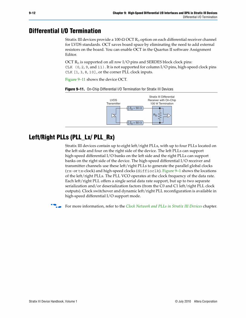
Differential I/O TerminationStratix III devices provide a 100- OCT RD option on each differential receiver channel for LVDS standards. OCT saves board space by eliminating the need to add external resistors on the board. You can enable OCT in the Quartus II software Assignment Editor.
OCT RD is supported on all row I/O pins and SERDES block clock pins:CLK (0, 2, 9, and 11). It is not supported for column I/O pins, high-speed clock pins CLK [1, 3, 8, 10], or the corner PLL clock inputs.
Figure 9–11 shows the device OCT.
Left/Right PLLs (PLL_Lx/ PLL_Rx)Stratix III devices contain up to eight left/right PLLs, with up to four PLLs located on the left side and four on the right side of the device. The left PLLs can support high-speed differential I/O banks on the left side and the right PLLs can support banks on the right side of the device. The high-speed differential I/O receiver and transmitter channels use these left/right PLLs to generate the parallel global clocks (rx- or tx-clock) and high-speed clocks (diffioclk). Figure 9–1 shows the locations of the left/right PLLs. The PLL VCO operates at the clock frequency of the data rate. Each left/right PLL offers a single serial data rate support, but up to two separate serialization and/or deserialization factors (from the C0 and C1 left/right PLL clock outputs). Clock switchover and dynamic left/right PLL reconfiguration is available in high-speed differential I/O support mode.
f For more information, refer to the Clock Network and PLLs in Stratix III Devices chapter.
Figure 9–11. On-Chip Differential I/O Termination for Stratix III Devices
LVDSTransmitter
Stratix III DifferentialReceiver with On-Chip
100 W Termination
RD
Z0 = 50 Ω
Z0 = 50 Ω
Stratix III Device Handbook, Volume 1 © July 2010 Altera Corporation

Chapter 9: High-Speed Differential I/O Interfaces and DPA in Stratix III Devices 9–13Left/Right PLLs (PLL_Lx/ PLL_Rx)
Figure 9–12 shows a simplified block diagram of the major components of the Stratix III PLL.
Figure 9–12. PLL Block Diagram for Stratix III Devices
Notes to Figure 9–12:
(1) n = 6 for Left/Right PLLs; n = 9 for Top/Bottom PLLs.(2) This is the VCO post-scale counter K.
(3) The FBOUT port is fed by the M counter in Stratix III PLLs.(4) The global or regional clock input can be driven by an output from another PLL, a pin-driven dedicated global or regional clock, or through a clock
control block provided the clock control block is fed by an output from another PLL or a pin-driven dedicated global or regional clock. An internally generated global signal or general purpose I/O pin cannot drive the PLL.
ClockSwitchover
Block
inclk0
inclk1
Clock inputsfrom pins
GCLK/RCLK
Cascade inputfrom adjacent PLL
pfdena
clkswitchclkbad0clkbad1activeclock
PFD
LockCircuit
locked
÷n CP LF VCO÷2(2)
84
FBINDIFFIOCLK networkGCLK/RCLK network
no compensation modeZDB, External feedback modesLVDS Compensation modeSource Synchronous, normal modes
÷C0
÷C1
÷C2
÷C3
÷Cn
÷m
(1)
PL
L O
utp
ut
Mu
x
Casade outputto adjacent PLL
GCLKs
RCLKs
External clockoutputs
DIFFIOCLK fromLeft/Right PLLs
LOAD_EN fromLeft/Right PLLs
FBOUT (3)
Externalmemoryinterface DLL
88
To DPA block onLeft/Right PLLs
/2, /4
(4)
© July 2010 Altera Corporation Stratix III Device Handbook, Volume 1

9–14 Chapter 9: High-Speed Differential I/O Interfaces and DPA in Stratix III DevicesClocking
ClockingThe left/right PLLs feed into the differential transmitter and receive channels through the LVDS and DPA clock network. The center left/right PLLs can clock the transmitter and receive channels above and below them. The corner left/right PLLs can drive I/Os in the banks adjacent to them. Figure 9–13 and Figure 9–14 show center and corner PLL clocking in Stratix III devices. You can find more information about PLL clocking restrictions in “Differential Pin Placement Guidelines” on page 9–19.
Figure 9–13. LVDS/DPA Clocks with Center PLLs for Stratix III Devices
Figure 9–14. LVDS/DPA Clocks with Center and Corner PLLs for Stratix III Devices
4
2
2
2
2
4
4
4
4
4
4
4
Quadrant Quadrant
Quadrant Quadrant
LVDSClock
Center PLL_L2
Center PLL_L3
DPAClock
LVDSClock
DPAClock
LVDSClock
CenterPLL_R2
CenterPLL_R3
DPAClock
LVDSClock
DPAClock
4
2
2
2
2
4
Quadrant Quadrant
Quadrant Quadrant
LVDSClock
Center PLL_L2
Center PLL_L3
LVDSClock
DPAClock
2
4
2
4
4
4
2
4
2
4
LVDSClock
CenterPLL_R2
CenterPLL_R3
DPAClock
LVDSClock
DPAClock
Corner PLL_L1
Corner PLL_L4
DPAClock
CornerPLL_R1
CornerPLL_R4
Stratix III Device Handbook, Volume 1 © July 2010 Altera Corporation

Chapter 9: High-Speed Differential I/O Interfaces and DPA in Stratix III Devices 9–15Clocking
Source-Synchronous Timing BudgetThis section discusses the timing budget, waveforms, and specifications for source-synchronous signaling in Stratix III devices. LVDS I/O standards enable high-speed data transmission. This high data transmission rate results in better overall system performance. To take advantage of fast system performance, it is important to understand how to analyze timing for these high-speed signals. Timing analysis for the differential block is different from traditional synchronous timing analysis techniques.
Rather than focusing on clock-to-output and setup times, source synchronous timing analysis is based on the skew between the data and the clock signals. High-speed differential data transmission requires the use of timing parameters provided by IC vendors and is strongly influenced by board skew, cable skew, and clock jitter. This section defines the source-synchronous differential data orientation timing parameters, the timing budget definitions for Stratix III devices, and ways to use these timing parameters to determine the maximum performance of your design.
Differential Data OrientationThere is a set relationship between an external clock and the incoming data. For an operation at 1 Gbps and SERDES factor of 10, the external clock is multiplied by 10, and phase-alignment can be set in the PLL to coincide with the sampling window of each data bit. The data is sampled on the falling edge of the multiplied clock. Figure 9–15 shows the data bit orientation of the ×10 mode.
Differential I/O Bit PositionData synchronization is necessary for successful data transmission at high frequencies. Figure 9–16 shows the data bit orientation for a channel operation. These figures are based on the following:
■ SERDES factor equals clock multiplication factor
■ Edge alignment is selected for phase alignment
■ Implemented in hard SERDES
For other serialization factors, use the Quartus II software tools and find the bit position within the word and the bit positions after deserialization.
Figure 9–15. Bit Orientation in Quartus II Software
9 8 7 6 5 4 3 2 1 0
10 LVDS BitsMSB LSB
inclock/outclock
data in
© July 2010 Altera Corporation Stratix III Device Handbook, Volume 1

9–16 Chapter 9: High-Speed Differential I/O Interfaces and DPA in Stratix III DevicesClocking
Table 9–3 lists the conventions for differential bit naming for 18 differential channels. The MSB and LSB positions increase with the number of channels used in a system.
Figure 9–16. Bit-Order and Word Boundary for One Differential Channel (Note 1)
Note to Figure 9–16:(1) These are only functional waveforms and are not intended to convey timing information.
Previous Cycle7 6 5 4 3 2 1 0
MSB LSB
tx_outclock
tx_out X X X X X X X X X X X X X X X XCurrent Cycle Next Cycle
Transmitter ChannelOperation (x8 Mode)
X X X X X X X X
rx_inclock
rx_in 7 6 5 4 3 2 1 0 X X X X X X X X X X X X X X X X
Receiver ChannelOperation (x8 Mode)
rx_inclock
rx_in
rx_outclock
rx_out [3..0]
X X X X X XX X X X X X
Receiver ChannelOperation (x4 Mode)
3 2 1 0
X X X X X X X X X X X X 3210
rx_outclock
rx_out [7..0] X X X X X X X X X X X X X X X X X X X X 7 6 5 4 3 2 1 0 X X X X
Table 9–3. Differential Bit Naming (Part 1 of 2)
Receiver Channel Data Number
Internal 8-Bit Parallel Data
MSB Position LSB Position
1 7 0
2 15 8
3 23 16
4 31 24
5 39 32
6 47 40
7 55 48
8 63 56
9 71 64
10 79 72
11 87 80
12 95 88
13 103 96
14 111 104
15 119 112
16 127 120
Stratix III Device Handbook, Volume 1 © July 2010 Altera Corporation

Chapter 9: High-Speed Differential I/O Interfaces and DPA in Stratix III Devices 9–17Clocking
Receiver Skew Margin for Non-DPAChanges in system environment, such as temperature, media (cable, connector, or PCB) loading effect, the receiver’s setup and hold times, and internal skew, reduce the sampling window for the receiver. The timing margin between the receiver’s clock input and the data input sampling window is called receiver skew margin (RSKM). Figure 9–17 shows the relationship between the RSKM and the sampling window of the receiver.
Transmit channel-to-channel skew (TCCS), RSKM, and the sampling window specifications are used for high-speed source-synchronous differential signals without DPA. When using DPA, these specifications are exchanged for the simpler single DPA jitter tolerance specification. For instance, the receiver skew is why each input with DPA selects a different phase of the clock, thus removing the requirement for this margin. In the timing diagram, TSW represents time for the sampling window.
17 135 128
18 143 136
Table 9–3. Differential Bit Naming (Part 2 of 2)
Receiver Channel Data Number
Internal 8-Bit Parallel Data
MSB Position LSB Position
© July 2010 Altera Corporation Stratix III Device Handbook, Volume 1

9–18 Chapter 9: High-Speed Differential I/O Interfaces and DPA in Stratix III DevicesClocking
Figure 9–17. Differential High-Speed Timing Diagram and Timing Budget for Non-DPA
RSKM
TUI
Time Unit Interval (TUI)
RSKM
TCCS
InternalClock
Falling Edge
tSW (min)Bit n
tSW (max)Bit n
RSKMTCCS
SamplingWindow
TCCS2
ReceiverInput Data
TransmitterOutput Data
InternalClockSynchronization
ExternalClock
ReceiverInput Data
InternalClock
ExternalInput Clock
Timing Budget
Timing Diagram
Clock Placement
SamplingWindow (SW) RSKM
TCCS
Stratix III Device Handbook, Volume 1 © July 2010 Altera Corporation

Chapter 9: High-Speed Differential I/O Interfaces and DPA in Stratix III Devices 9–19Differential Pin Placement Guidelines
Differential Pin Placement GuidelinesTo ensure proper high-speed operation, differential pin placement guidelines have been established. The Quartus II compiler automatically checks that these guidelines are followed and issues an error message if they are not met.
Because DPA usage adds some constraints on the placement of high-speed differential channels, this section is divided into pin placement guidelines with and without DPA usage.
Guidelines for DPA-Enabled Differential ChannelsThe Stratix III device has differential receivers and transmitters in I/O banks on the left and right sides of the device. Each receiver has a dedicated DPA circuit to align the phase of the clock to the data phase of its associated channel. When DPA-enabled channels are used in differential banks, you must adhere to the guidelines listed in the following sections.
DPA-Enabled Channels and Single-Ended I/OsWhen there is a DPA channel enabled in a bank, both single-ended I/Os and differential I/O standards are allowed in the bank.
Single-ended I/Os are allowed in the same I/O bank as long as the single-ended I/O standard uses the same VCCIO as the DPA-enabled differential I/O bank.
DPA-Enabled Channel Driving DistanceIf the number of DPA channels driven by each left/right PLL exceeds 25 LAB rows, Altera recommends implementing data realignment (bit-slip) circuitry for all the DPA channels.
Using Corner and Center Left/Right PLLsIf a differential bank is being driven by two left/right PLLs, where the corner left/right PLL is driving one group and the center left/right PLL is driving another group, there must be at least one row of separation between the two groups of DPA-enabled channels (refer to Figure 9–18). The two groups can operate at independent frequencies.
No separation is necessary if a single left/right PLL is driving DPA-enabled channels as well as DPA-disabled channels.
© July 2010 Altera Corporation Stratix III Device Handbook, Volume 1

9–20 Chapter 9: High-Speed Differential I/O Interfaces and DPA in Stratix III DevicesDifferential Pin Placement Guidelines
Figure 9–18. Corner and Center Left/Right PLLs Driving DPA-Enabled Differential I/Os in the Same Bank
Center
Left /Right PLL
Corner
Left /Right PLL
Diff I/O
DPA-enabled Diff I/O
DPA-enabled Diff I/O
DPA-enabled
Diff I/O
DPA-enabled
Diff I/O
Channels
driven by
Corner
Left/Right PLL
Channels
driven by
Center
Left/Right
PLL
One Unused
Channel for Buffer
DPA-enabled
Diff I/O
DPA -enabled
Diff I/O
DPA -enabled
Diff I/O
DPA -enabled
Diff I/O
DPA -enabled
Diff I/O
Reference
Reference CLK
CLK
Stratix III Device Handbook, Volume 1 © July 2010 Altera Corporation

Chapter 9: High-Speed Differential I/O Interfaces and DPA in Stratix III Devices 9–21Differential Pin Placement Guidelines
Using Both Center Left/Right PLLsBoth center left/right PLLs can be used to drive DPA-enabled channels simultaneously, as long as they drive these channels in their adjacent banks only, as shown in Figure 9–19.
If one of the center left/right PLLs drive the top and bottom banks, the other center left/right PLL cannot be used to drive the differential channels, as shown in Figure 9–19.
If the top PLL_L2/PLL_R2 drives DPA-enabled channels in the lower differential bank, the PLL_L3/PLL_R3 cannot drive DPA-enabled channels in the upper differential banks and vice versa. In other words, the center left/right PLLs cannot drive cross-banks simultaneously, as shown in Figure 9–20.
Figure 9–19. Center Left/Right PLLs Driving DPA-Enabled Differential I/Os
ReferenceCLK
DPA-enabledDiff I/O
DPA-enabledDiff I/O
DPA-enabledDiff I/O
DPA-enabledDiff I/O
DPA-enabledDiff I/O
DPA-enabledDiff I/O
DPA-enabledDiff I/O
DPA-enabledDiff I/O
DPA-enabledDiff I/O
DPA-enabledDiff I/O
DPA-enabledDiff I/O
CenterLeft/Right PLL
(PLL_L2/PLL_R2)
CenterLeft/Right PLL
(PLL_L2/PLL_R2)
CenterLeft/Right PLL
(PLL_L3/PLL_R3)
CenterLeft/Right PLL
(PLL_L3/PLL_R3)
UnusedPLL
Reference CLK
Reference CLK
Reference CLK
DPA-enabledDiff I/O
DPA-enabledDiff I/O
DPA-enabledDiff I/O
DPA-enabledDiff I/O
DPA-enabledDiff I/O
© July 2010 Altera Corporation Stratix III Device Handbook, Volume 1

9–22 Chapter 9: High-Speed Differential I/O Interfaces and DPA in Stratix III DevicesDifferential Pin Placement Guidelines
Figure 9–20. Invalid Placement of DPA-Enabled Differential I/Os Driven by Both Center Left/Right PLLs
DPA-enabled
Diff I/O
Center Left /Right
PLL
DPA-enabled
Diff I/O
DPA-enabled
Diff I/O
Reference
CLK
Reference
CLK
DPA-enabled
Diff I/O
DPA-enabled
Diff I/O
DPA-enabled Diff I/O
Center Left /Right
PLL
DPA-enabled
Diff I/O
DPA-enabled Diff I/O
Stratix III Device Handbook, Volume 1 © July 2010 Altera Corporation

Chapter 9: High-Speed Differential I/O Interfaces and DPA in Stratix III Devices 9–23Differential Pin Placement Guidelines
Guidelines for DPA-Disabled Differential ChannelsWhen DPA-disabled channels are used in the left and right banks of a Stratix III device, you must adhere to the guidelines in the following sections.
DPA-Disabled Channels and Single-Ended I/OsThe placement rules for DPA-disabled channels and single-ended I/Os are the same as those for DPA-enabled channels and single-ended I/Os.
DPA-Disabled Channel Driving DistanceEach left/right PLL can drive all the DPA-disabled channels in the entire bank.
Using Corner and Center Left/Right PLLsA corner left/right PLL can be used to drive all transmitter channels and a center left/right PLL can be used to drive all DPA-disabled receiver channels within the same differential bank. In other words, a transmitter channel and a receiver channel in the same LAB row can be driven by two different PLLs, as shown in Figure 9–21.
A corner left/right PLL and a center left/right PLL can drive duplex channels in the same differential bank as long as the channels driven by each PLL are not interleaved. No separation is necessary between the group of channels driven by the corner and center left/right PLLs. Refer to Figure 9–21 and Figure 9–22.
© July 2010 Altera Corporation Stratix III Device Handbook, Volume 1

9–24 Chapter 9: High-Speed Differential I/O Interfaces and DPA in Stratix III DevicesDifferential Pin Placement Guidelines
Figure 9–21. Corner and Center Left/Right PLLs Driving DPA-Disabled Differential I/Os in the Same Bank
Diff RX
Corner Left/Right PLL
Diff TX
Diff RX Diff TX
Diff RX Diff TX
Diff RX Diff TX
Diff RX Diff TX
Diff RX Diff TX
Diff RX Diff TX
Diff RX Diff TX
Diff RX Diff TX
Diff RX Diff TX
Corner Left/Right
PLL
DPA-disabled Diff I/O
Channels driven by Corner
Left /Right PLL
Channels driven by Center
Left /Right PLL
No separation
buffer needed
Reference CLK
Reference CLK
Reference CLK
Reference CLK
DPA-disabledDiff I/O
DPA-disabledDiff I/O
DPA-disabledDiff I/O
DPA-disabledDiff I/O
DPA-disabledDiff I/O
DPA-disabledDiff I/O
DPA-disabledDiff I/O
DPA-disabledDiff I/O
DPA-disabledDiff I/O
Center Left/RightPLL
Center Left/RightPLL
Stratix III Device Handbook, Volume 1 © July 2010 Altera Corporation

Chapter 9: High-Speed Differential I/O Interfaces and DPA in Stratix III Devices 9–25Differential Pin Placement Guidelines
Figure 9–22. Invalid Placement of DPA-Disabled Differential I/Os Due to Interleaving of Channels Driven by the Corner and Center Left/Right PLLs
DPA-disabledDiff I/O
DPA-disabledDiff I/O
DPA-disabledDiff I/O
DPA-disabledDiff I/O
DPA-disabledDiff I/O
DPA-disabledDiff I/O
DPA-disabledDiff I/O
DPA-disabledDiff I/O
Corner Left/Right PLL
Reference CLK
DPA-disabledDiff I/O
DPA-disabledDiff I/O
Reference CLK
Center Left/RightPLL
© July 2010 Altera Corporation Stratix III Device Handbook, Volume 1

9–26 Chapter 9: High-Speed Differential I/O Interfaces and DPA in Stratix III DevicesDifferential Pin Placement Guidelines
Using Both Center Left/Right PLLsBoth center left/right PLLs can be used simultaneously to drive DPA-disabled channels on upper and lower differential banks. Unlike DPA-enabled channels, the center left/right PLLs can drive cross-banks. For example, the upper center left/right PLL can drive the lower differential bank at the same time the lower center left/right PLL is driving the upper differential bank and vice versa, as shown in Figure 9–23.
Figure 9–23. Both Center Left/Right PLLs Driving Cross-Bank DPA-Disabled Channels Simultaneously
DPA-disabledDiff I/O
DPA-disabledDiff I/O
DPA-disabledDiff I/O
DPA-disabledDiff I/O
DPA-disabledDiff I/O
DPA-disabledDiff I/O
DPA-disabledDiff I/O
DPA-disabledDiff I/O
ReferenceCLK
ReferenceCLK
CenterLeft/Right PLL
CenterLeft/Right PLL
Stratix III Device Handbook, Volume 1 © July 2010 Altera Corporation

Chapter 9: High-Speed Differential I/O Interfaces and DPA in Stratix III Devices 9–27Chapter Revision History
Chapter Revision HistoryTable 9–4 lists the revision history for this chapter.
Table 9–4. Chapter Revision History
Date Revision Changes Made
July 2010 1.9 Updated “Differential Transmitter” and “Differential Receiver” sections.
March 2010 1.8
Updated for the Quartus II software version 9.1 SP2 release:
■ Updated “LVDS Channels”, “Differential Transmitter”, and “Differential Receiver” section.
■ Minor changes to the text.
May 2009 1.7
■ Updated Table 9–1 and Table 9–2.
■ Updated Figure 9–5.
■ Updated “DPA-Enabled Channels and Single-Ended I/Os” section.
February 2009 1.6
■ Updated “DPA-Enabled Channels and Single-Ended I/Os” section.
■ Updated Table 9–2.
■ Removed “Reference Documents” section.
October 2008 1.5
■ Updated “Introduction”, “Differential Receiver”, and “Synchronizer” sections.
■ Updated Figure 9–5.
■ Updated New Document Format.
May 2008 1.4
■ Updated “Soft-CDR Mode”, “Dynamic Phase Aligner (DPA)”, “Programmable Pre-Emphasis and Programmable VOD”, and “Guidelines for DPA-Enabled Differential Channels” sections.
■ Updated Table 9–1 and Table 9–2.
■ Removed “Figure 9–19. Left/Right PLL Driving Distance for DPA-Enabled Channels”.
November 2007 1.3 ■ Updated Table 9–1 and Table 9–2.
October 2007 1.2
■ Added material to “DPA-Enabled Channels and Single-Ended I/Os” on page 9–21 and removed material from “DPA-Disabled Channels and Single-Ended I/Os” on page 9–29.
■ Added new sections “Programmable Pre-Emphasis and Programmable VOD” on page 9–12, “Soft-CDR Mode”, and “Referenced Documents”.
■ Added live links for references.
■ Added Figure 9–10.
■ Minor edits to “DPA-Enabled Channel Driving Distance” section.
May 2007 1.1■ Minor changes to second paragraph of the section “Differential I/O
Termination”.
■ Added Table 9–1 and Table 9–2.
November 2006 1.0 Initial release.
© July 2010 Altera Corporation Stratix III Device Handbook, Volume 1

9–28 Chapter 9: High-Speed Differential I/O Interfaces and DPA in Stratix III DevicesChapter Revision History
Stratix III Device Handbook, Volume 1 © July 2010 Altera Corporation